EP1858089A2 - Semiconductor optical device - Google Patents
Semiconductor optical device Download PDFInfo
- Publication number
- EP1858089A2 EP1858089A2 EP07009978A EP07009978A EP1858089A2 EP 1858089 A2 EP1858089 A2 EP 1858089A2 EP 07009978 A EP07009978 A EP 07009978A EP 07009978 A EP07009978 A EP 07009978A EP 1858089 A2 EP1858089 A2 EP 1858089A2
- Authority
- EP
- European Patent Office
- Prior art keywords
- lead frame
- semiconductor optical
- resin
- optical device
- encapsulating
- Prior art date
- Legal status (The legal status is an assumption and is not a legal conclusion. Google has not performed a legal analysis and makes no representation as to the accuracy of the status listed.)
- Withdrawn
Links
Images







Classifications
-
- H—ELECTRICITY
- H10—SEMICONDUCTOR DEVICES; ELECTRIC SOLID-STATE DEVICES NOT OTHERWISE PROVIDED FOR
- H10F—INORGANIC SEMICONDUCTOR DEVICES SENSITIVE TO INFRARED RADIATION, LIGHT, ELECTROMAGNETIC RADIATION OF SHORTER WAVELENGTH OR CORPUSCULAR RADIATION
- H10F77/00—Constructional details of devices covered by this subclass
- H10F77/50—Encapsulations or containers
-
- H—ELECTRICITY
- H10—SEMICONDUCTOR DEVICES; ELECTRIC SOLID-STATE DEVICES NOT OTHERWISE PROVIDED FOR
- H10H—INORGANIC LIGHT-EMITTING SEMICONDUCTOR DEVICES HAVING POTENTIAL BARRIERS
- H10H20/00—Individual inorganic light-emitting semiconductor devices having potential barriers, e.g. light-emitting diodes [LED]
- H10H20/80—Constructional details
- H10H20/85—Packages
- H10H20/8506—Containers
-
- H—ELECTRICITY
- H10—SEMICONDUCTOR DEVICES; ELECTRIC SOLID-STATE DEVICES NOT OTHERWISE PROVIDED FOR
- H10H—INORGANIC LIGHT-EMITTING SEMICONDUCTOR DEVICES HAVING POTENTIAL BARRIERS
- H10H20/00—Individual inorganic light-emitting semiconductor devices having potential barriers, e.g. light-emitting diodes [LED]
- H10H20/80—Constructional details
- H10H20/85—Packages
- H10H20/857—Interconnections, e.g. lead-frames, bond wires or solder balls
-
- H—ELECTRICITY
- H10—SEMICONDUCTOR DEVICES; ELECTRIC SOLID-STATE DEVICES NOT OTHERWISE PROVIDED FOR
- H10H—INORGANIC LIGHT-EMITTING SEMICONDUCTOR DEVICES HAVING POTENTIAL BARRIERS
- H10H20/00—Individual inorganic light-emitting semiconductor devices having potential barriers, e.g. light-emitting diodes [LED]
- H10H20/80—Constructional details
- H10H20/85—Packages
- H10H20/858—Means for heat extraction or cooling
- H10H20/8585—Means for heat extraction or cooling being an interconnection
-
- H—ELECTRICITY
- H10—SEMICONDUCTOR DEVICES; ELECTRIC SOLID-STATE DEVICES NOT OTHERWISE PROVIDED FOR
- H10W—GENERIC PACKAGES, INTERCONNECTIONS, CONNECTORS OR OTHER CONSTRUCTIONAL DETAILS OF DEVICES COVERED BY CLASS H10
- H10W72/00—Interconnections or connectors in packages
- H10W72/50—Bond wires
- H10W72/531—Shapes of wire connectors
- H10W72/536—Shapes of wire connectors the connected ends being ball-shaped
-
- H—ELECTRICITY
- H10—SEMICONDUCTOR DEVICES; ELECTRIC SOLID-STATE DEVICES NOT OTHERWISE PROVIDED FOR
- H10W—GENERIC PACKAGES, INTERCONNECTIONS, CONNECTORS OR OTHER CONSTRUCTIONAL DETAILS OF DEVICES COVERED BY CLASS H10
- H10W72/00—Interconnections or connectors in packages
- H10W72/50—Bond wires
- H10W72/531—Shapes of wire connectors
- H10W72/5363—Shapes of wire connectors the connected ends being wedge-shaped
-
- H—ELECTRICITY
- H10—SEMICONDUCTOR DEVICES; ELECTRIC SOLID-STATE DEVICES NOT OTHERWISE PROVIDED FOR
- H10W—GENERIC PACKAGES, INTERCONNECTIONS, CONNECTORS OR OTHER CONSTRUCTIONAL DETAILS OF DEVICES COVERED BY CLASS H10
- H10W90/00—Package configurations
-
- H—ELECTRICITY
- H10—SEMICONDUCTOR DEVICES; ELECTRIC SOLID-STATE DEVICES NOT OTHERWISE PROVIDED FOR
- H10W—GENERIC PACKAGES, INTERCONNECTIONS, CONNECTORS OR OTHER CONSTRUCTIONAL DETAILS OF DEVICES COVERED BY CLASS H10
- H10W90/00—Package configurations
- H10W90/701—Package configurations characterised by the relative positions of pads or connectors relative to package parts
- H10W90/751—Package configurations characterised by the relative positions of pads or connectors relative to package parts of bond wires
- H10W90/756—Package configurations characterised by the relative positions of pads or connectors relative to package parts of bond wires between a chip and a stacked lead frame, conducting package substrate or heat sink
Definitions
- a surface mount semiconductor optical device having a semiconductor optical chip mounted in a casing that is provided with lead frame electrodes insert-formed by a resin includes the following two types. One is a top view type, in which a light ray axis is perpendicular to a circuit board on which the chip is mounted. The other is a side view type, in which a light ray axis is parallel to the circuit board.
- Figs. 15 is a front view showing the semiconductor optical device of Figs. 1 (a)-(d) mounted on a circuit board;
- the casing 2 can be substantially cuboid and can be provided with a concave-shaped cavity 6 with an opening 5 and a bottom portion.
- each of the pairs of lead frame electrodes 3a, 3b can extend from respective one end portions 7a, 7b and can protrude or extend from outside surfaces 8c', 8d', etc. of the casing 2 to an outside area.
- the encapsulating resin 12 can be disposed in the concave-shaped cavity portion 6 of the casing 2 as described above and can encapsulate semiconductor optical chips 4 and bonding wire 13 therein.
Landscapes
- Led Device Packages (AREA)
- Light Receiving Elements (AREA)
Abstract
Description
- This application claims the priority benefit under 35 U.S.C. §119 of
Japanese Patent Application No. 2006-139095 filed on May 18, 2006 - The presently disclosed subject matter relates to a semiconductor optical device including LEDs, laser diodes, photodiodes, etc. and more particularly to a surface mount semiconductor optical device, which emits/detects light in parallel with a mounting surface thereof (e.g., a side view type semiconductor device).
- A surface mount semiconductor optical device having a semiconductor optical chip mounted in a casing that is provided with lead frame electrodes insert-formed by a resin includes the following two types. One is a top view type, in which a light ray axis is perpendicular to a circuit board on which the chip is mounted. The other is a side view type, in which a light ray axis is parallel to the circuit board.
- A semiconductor optical device of the side view type is generally used as a light source for use with a light guide material in a flat panel display, which is used as a back light unit for a LCD panel, a panel lighting apparatus, general lighting and the like.
- The structure shown in Fig. 16 is a typical structure for a conventional semiconductor
optical device 52 of the side view type. The structure includes acasing 51 that is provided with lead frame electrodes 50(a), 50(c), 50(b), 50(d) insert-formed by a resin. Thecasing 51 includes a concave-shaped cavity with an opening and a bottom portion at which eachend portion other end portion optical device 52. Theother end portions casing 51. - An
LED chip 53 is mounted on the exposedend portion 50a via a conductive material and is electrically connected at one electrode thereof to the exposedend portion 50a. The other electrode of theLED chip 53 is electrically connected to the exposedend portion 50b via abonding wire 54. An encapsulating transparent resin is disposed in the concave-shaped cavity for encapsulatingchips 53 andbonding wires 54. A semiconductor optical device such as a surface mount LED device of the side view type is described in further detail, for example, inJapanese Patent Application Laid Open JP2004-193537 - Because an LED chip used for the above-described conventional semiconductor optical device is made from semiconductor materials, the electrical and optical characteristics thereof are dependent on temperature. That is, when a current flows to an LED chip and the LED chip is lit, a light-emitting efficiency thereof decreases due to a self fever condition caused by an LED current that flows into the LED chip and elevates the temperature of the MED chip.
- Thus, in order to prevent the decrease of the light-emitting efficiency one can radiate the self-fever, which is generated during light-emitting of the LED chip. The self-fever generated in an LED chip may be generally radiated from an LED chip to an area outside of the semiconductor optical device through the lead frame electrodes that include an LED chip mounted thereon. The lead frame electrodes may greatly contribute to the prevention of the self-fever condition in an LED chip both directly and indirectly. Therefore, effective radiation characteristic design for the lead frame electrode is an important factor for preventing a rise of the self-fever during light-emitting of the LED chip.
- When the above-described conventional semiconductor
optical device 52 is considered, both the one lead frame electrode mounted an LED chip on the exposed one end portion thereof and the other lead frame electrode connected to the exposed end portion thereof via a bonding wire extend into the same surface of the concave-shaped cavity to and from the same outside surface. - In a surface mount semiconductor optical device that is miniaturized, the greater the amount of lead frame electrodes that lead from the casing to the outside, the narrower the width of each lead frame electrode is in order to maintain a miniaturization of the device size.
- However, the narrower the width of the lead frame electrode, the smaller the cross-sectional area that is perpendicular to current flow direction in the LED becomes. As a result, a thermal conduction decrease of the lead frame electrode is caused by an increase of thermal resistance, and may result in a loss of radiation ability.
- The lead frame electrode is generally formed by stamping out a sheet metal using a press die. Each interval in the sheet metal between respective adjacent lead frame electrodes should at least be wider than a thickness of the lead frame electrode by restriction of the pressing process. Thus, the increase in the number of lead frame electrodes results in a restrictive factor for designing a miniaturization of a semiconductor optical device size.
- If the number of lead frame electrodes increases, each area at the other end portions of lead frame electrodes that leads from the casing should be small due to a layout restriction, e.g., for maintaining a predetermined interval between respective adjacent lead frame electrodes. When the semiconductor optical device is mounted on a circuit board, the function of the other end portions includes: fixing the device to the circuit board by mounting on conductor patterns of a circuit board; electrically connecting the device to a circuit board; and conducting the self-fever of LED chips to conductor patterns of a circuit board through the lead frame electrodes upon which LED chips are mounted.
- If the area of respective other end portions of the lead frame electrodes becomes small, the contact area with conductor patterns of a circuit board becomes small. Thus, the decrease in area of respective other end portions may result in a decrease of mounting reliability because the semiconductor optical device may not be mounted with strength and confidence by the respective other end portions, and may result in a decrease of the light-emitting efficiency due to a rise of the operating temperature of an LED chip by weakening radiating efficiency of the LED chip's self-fever.
- Furthermore, when a complex light-emitting color is emitted by a plurality of different light-emitting color LED chips, it is difficult to maintain a miniaturization of a semiconductor optical device size and to provide equal spacing intervals for the respective adjacent LED chips due to layout restrictions of the lead frame electrodes when positions of the one end portions must be moved in accordance with a layout of LED chips. If each interval of the respective adjacent LED chips is forced to be equal, a semiconductor optical device may become large and may result in a decrease in the color rendering index because of long intervals between respective adjacent LED chips.
- The disclosed subject matter has been devised in consideration of the above and other problems and characteristics. The disclosed subject matter can include a semiconductor optical device, which includes a stable optical characteristic with an excellent radiant efficiency, a high mounting reliability, and a possibility for design miniaturization.
- The presently disclosed subject matter has been devised in view of the above and other characteristics problems and features and includes a semiconductor optical device with high mounting reliability and the possibility of miniaturization. Another aspect of the disclosed subject matter includes a semiconductor light-emitting device that emits various light-emitting colors with excellent optical characteristics.
- According to an aspect of the disclosed subject matter, a semiconductor optical devices can include: a casing formed substantially cuboid by a resin, the casing having a concave-shaped cavity with an opening and a bottom portion; at least one first lead frame electrode with one end portion thereof disclosed on the bottom portion, the at least one first lead frame electrode being led onto either outside surface that is substantially perpendicular to the bottom portion and being bent substantially perpendicular at the outside surface in the direction of the opening; at least one second lead frame electrode corresponding to the at least one first electrode, with one end portion thereof disclosed on the bottom portion, the at least one second lead frame electrode being led onto an outside surface opposite to the outside surface whereon the at least one first lead frame electrode is led and/or being led onto at least one outside surface that is substantially perpendicular to the outside surface whereon the at least one first lead frame electrode is led, being bent substantially perpendicular at the respective outside surfaces in the direction of the opposite side of the opening and other end portion thereof being led to the substantially same level as the at least one first lead frame electrode; and at least one semiconductor optical chip being mounted on the one end portion of the at least one first lead frame electrode, one electrode thereof being electrically connected to the one end portion of the at least one first lead frame electrode, and other electrode thereof being electrically connected to the other end portion of the corresponding at least one second lead frame electrode of the at least one first lead frame electrode.
- In the immediate above described exemplary semiconductor optical devices, the at least one second lead frame electrode may be further bent substantially perpendicular in the direction of the other end portion of the at least one first lead frame electrode or may be further bent substantially perpendicular in the direction opposite to the other end portion of the at least one first lead frame electrode.
- According to an modifiable aspect of the disclosed subject matter, semiconductor optical devices can include: a casing formed substantially cuboid by a resin, the casing having a concave-shaped cavity with an opening and a bottom portion; at least one first lead frame electrode with one end portion thereof disclosed on the bottom portion, the at least one first lead frame electrode being led onto either outside surface that is substantially perpendicular to the bottom portion and being bent substantially perpendicular at the outside surface in the direction opposite to the opening; at least one second lead frame electrode corresponding to the at least one first lead frame electrode, with one end portion thereof disclosed on the bottom portion, the at least one second lead frame electrode being led onto a outside surface opposite to the outside surface whereon the at least one first lead frame electrode is led and/or being led onto at least one outside surface that is substantially perpendicular to the outside surface whereon the at least one first lead frame electrode is led, being bent substantially perpendicular at the respective outside surfaces in the direction of the opening and other end thereof being led to the substantially same level as the at least one first lead frame electrode; and at least one semiconductor optical chip being mounted on the one end portion of the at least one first lead frame electrode, one electrode thereof being electrically connected to the one end portion of the at least one first lead frame electrode, and other electrode thereof being electrically connected to the other end portion of the corresponding at least one second lead frame electrode of the at least one first lead frame electrode.
- In the above described exemplary optical devices, the at least one second lead frame electrode may be further bent substantially perpendicular onto the outside surface whereon the at least one first lead frame electrode is led.
- In the above described exemplary semiconductor optical devices, the at least one first lead frame electrode may be further led onto an outside surface substantially perpendicular to the outside surface whereon the at least one first lead frame electrode is led.
- In the above described exemplary semiconductor optical devices, each of the first lead frame electrodes may be bent in the opposite direction of each adjacent first lead frame electrode among these first lead frame electrodes that are led from the bottom portion of the concave-shaped cavity to either outside surface of the casing.
- Another of the aspects of the disclosed subject matter includes semiconductor optical devices that can include: an encapsulating resin made of at least one of a transparent resin and a mixture resin that includes a resin mixed with at least one of a diffuser, a phosphor, and a pigment for selectively absorbing light having a predetermined wavelength can be disposed in the concave-shaped cavity; and at least one semiconductor light-emitting chip that is configured as a semiconductor optical chip.
- These and other characteristics and features of the disclosed subject matter will become clear from the following description with reference to the accompanying drawings, wherein:
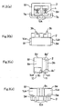
- Figs. 1 (a)-(d) are a front view, a top view, a side view and a bottom view in turn for a first embodiment of a semiconductor optical device made in accordance with principles of the disclosed subject matter;
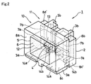
- Fig. 2 is a perspective view for the semiconductor optical device according to the first exemplary embodiment of Figs. 1(a)-(d);
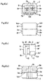
- Fig. 3(a)-(d) are a front view, a top view, a side view and a bottom view for a second exemplary embodiment of a semiconductor optical device made in accordance with principles of the disclosed subject matter;
- Figs. 4(a)-(d) are a front view, a top view, a side view and a bottom view for a third exemplary embodiment of a semiconductor optical device made in accordance with principles of the disclosed subject matter;
- Figs. 5(a)-(d) are a front view, a top view, a side view and a bottom view for a fourth exemplary embodiment of a semiconductor optical device made in accordance with principles of the disclosed subject matter;
- Figs. 6(a)-(d) are a front view, a top view, a side view and a bottom view for a fifth exemplary embodiment of a semiconductor optical device made in accordance with principles of the disclosed subject matter;
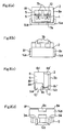
- Figs. 7(a)-(d) are a front view, a top view, a side view and a bottom view for a sixth exemplary embodiment of a semiconductor optical device made in accordance with principles of the disclosed subject matter;
- Figs. 8(a)-(d) are a front view, a top view, a side view and a bottom view for a seventh exemplary embodiment of a semiconductor optical device made in accordance with principles of the disclosed subject matter;
- Figs. 9(a)-(d) are a front view, a top view, a side view and a bottom view for an eighth exemplary embodiment of a semiconductor optical device made in accordance with principles of the disclosed subject matter;
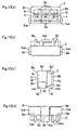
- Figs. 10(a)-(d) are a front view, a top view, a side view and a bottom view for a ninth exemplary embodiment of a semiconductor optical device made in accordance with principles of the disclosed subject matter;
- Figs. 11 (a)-(d) are a front view, a top view, a side view and a bottom view for a tenth exemplary embodiment of a semiconductor optical device made in accordance with principles of the disclosed subject matter;
- Figs. 12(a)-(d) are a front view, a top view, a side view and a bottom view for an eleventh exemplary embodiment of a semiconductor optical device made in accordance with principles of the disclosed subject matter;
- Figs. 13(a)-(d) are a front view, a top view, a side view and a bottom view for a twelfth exemplary embodiment of a semiconductor optical device made in accordance with principles of the disclosed subject matter;
- Figs. 14(a)-(d) are a front view, a top view, a side view and a bottom view for a thirteenth exemplary embodiment of a semiconductor optical device made in accordance with 1 principles of the disclosed subject matter;
- Figs. 15 is a front view showing the semiconductor optical device of Figs. 1 (a)-(d) mounted on a circuit board; and
- Fig. 16 is a perspective view depicting a conventional semiconductor optical device.
- A first exemplary embodiment of the disclosed subject matter will now be described in detail with reference to Figs. 1 (a)-(d) and Fig. 2. Figs. 1 (a)-(d) show a front view, a top view, a side view, and a bottom view in turn for a semiconductor optical device in accordance with the first exemplary embodiment, and Fig.2 shows the perspective view of the above device shown by Figs. 1(a)-(d).
- The semiconductor
optical device 1 in accordance with the first exemplary embodiment can include: acasing 2 made from a resin; two pairs oflead frame electrodes optical chips 4 having at least one of a light emitting/detecting function. - Actually, the
casing 2 can consist of a resin formation, and at least one pair oflead frame electrodes casing 2. Thecasing 2 defines the resin formation not including the pairs oflead frame electrodes - The
casing 2 can be substantially cuboid and can be provided with a concave-shapedcavity 6 with anopening 5 and a bottom portion. Each of the oneend portions lead frame electrodes cavity 6. In addition, each of the pairs oflead frame electrodes end portions outside surfaces 8c', 8d', etc. of thecasing 2 to an outside area. - A surface of the bottom portion of the concave-shaped
cavity 6 can be in a position substantially at the same level as the exposed surfaces of each oneend portion lead frame electrodes casing 2 can consist of a concave-shapedcavity formation 10 and a lead frameelectrode layout portion 11 on either side of the surface of the bottom portion. - Furthermore, an encapsulating
resin 12 made of at least one of a transparent resin and a mixture resin which includes a resin mixed with at least one of a diffuser, a phosphor, and a pigment for selectively absorbing light having a predetermined wavelength can be disposed in the concave-shapedcavity 6. The encapsulating resin can encapsulate the semiconductoroptical chips 4 andbonding wires 13 described later. - The semiconductor
optical chips 4 can be mounted in the concave-shapedcavity 6. The semiconductoroptical chips 4 can include the following characteristics individually or in combination: all being composed of at least one semiconductor chip having only a light-emitting function; all being composed of at least one semiconductor chip having only a light-detecting function; and being composed of a mixture of chips that include both the semiconductor optical chips having the light-emitting/detecting functions. - When the semiconductor optical chips are all composed of semiconductor light-emitting chips, the semiconductor optical chips can also include the following characteristics: all being composed of same color light-emitting chips; and being composed of a plurality of different color light-emitting chips.
- With respect to the specific semiconductor optical devices, the semiconductor light-emitting chips can be formed as a light emitting diode (LED), a laser diode, etc. and the semiconductor light-detecting chips can be formed as a photodiode, a phototransistor, and the like.
- The encapsulating
resin 12 can be figured to protect against outside circumstances such as moisture, dust, gas and the like, and to protect thebonding wires 13 3 from outside forces like vibration, shock, etc. When the semiconductor optical device is composed of at least one semiconductor light-emitting chip, the encapsulatingresin 12 can also function to improve a light-producing efficiency of light received from a light-emitting surface of the semiconductor light-emitting chip by forming an interface member between the light-emitting surface of the semiconductor light-emitting chip and theresin 12, and by creating a refractive index that is similar for both the interface member and a semiconductor material of the light-emitting surface of the semiconductor light-emitting chip. - A wavelength conversion material may be mixed in the encapsulating
resin 12 when the semiconductor optical device is composed of all semiconductor light-emitting chips. The semiconductor optical device can emit light of various color tone different from the light-emitting color of at least one semiconductor light-emitting chip through action of the wavelength conversion material, by selecting both the light-emitting color and the wavelength conversion material. - More specific description of a case in which a semiconductor optical device is composed of semiconductor light-emitting chips all having the same light-emitting color will now be given. When the above semiconductor light-emitting chip emits blue light (blue LED chip), the semiconductor optical device can emit light of approximately white color tone through use of an encapsulating resin mixed with a wavelength conversion material for converting blue light to a complementary yellow light. A part of the blue light emitted from a blue LED chip excites the wavelength conversion material and converts it to yellow light, which can be mixed with other parts of the blue light emitted from a blue LED chip by means of additive color mixture. Thus, the semiconductor optical device can emit light having an approximately white color tone.
- The semiconductor optical device can also emit light of approximately white color tone through an encapsulating resin that is mixed with two wavelength conversion materials for converting blue light to green light and/or red light. A part of the blue light emitted from a blue LED chip excites the two wavelength conversion materials and converts the light to green light and/or red light, which can be added to or mixed with other parts of the blue light emitted from the blue LED chip to generate an approximately white light by means of additive color mixture.
- When the above semiconductor light-emitting chip emits ultraviolet light (ultraviolet LED chip), the semiconductor optical device can also emit light of approximately white color tone through use of an encapsulating resin that is mixed with three kinds of wavelength conversion materials for converting ultraviolet light to blue light, green light and red light. The ultraviolet light emitted from ultraviolet LED chip excites the three wavelength conversion materials and converts the light to blue light, green light and red light, which can be added to generate approximately white light by means of additive color mixture.
- Furthermore, when the wavelength of light emitted from an LED chip and the type of wavelength conversion material are appropriately selected and combined, light of various color tone other than white light can be generated.
- When the semiconductor light-emitting chips are composed of a plurality of light-emitting chips of different light-emitting colors, light of various color tone other than the light-emitting color of the light-emitting chips can be generated through an encapsulating resin that is mixed with a wavelength conversion material.
- The light diffuser can provide the following characteristics: uniformity of luminance distribution emitted from a semiconductor light-emitting chip; a light mixture characteristic emitted from the semiconductor light-emitting chips when the semiconductor light-emitting chips are composed of a plurality of light-emitting chips of different light-emitting colors.
- The above-described structures can be common in the exemplary embodiments of the disclosed subject matter. Each of the exemplary embodiments will now be described in detail.
- Figs. 1 (a)-(d) show a front view, a top view, a side view and a bottom view for the semiconductor optical device in accordance with the first exemplary embodiment. Fig. 2 shows a perspective view for the semiconductor optical device in accordance with Figs. 1 (a)-(d).
- The semiconductor optical device can include two pairs of
lead frame electrodes end portions cavity 6 and being disposed four corners of the bottom portion that is substantially rectangular. - Each adjacent one
end portion 7a of the twolead frame electrodes 3a can include a semiconductoroptical chip 4 mounted thereon and can be electrically connected to a bottom of the electrodes of the semiconductoroptical chips 4. Each adjacent oneend portion 7b of the other twolead frame electrodes 3b can be disposed at opposite sides of each adjacent oneend portion 7a and can be electrically connected throughbonding wires 13 to upper electrodes of the semiconductoroptical chips 4. - The two
lead frame electrodes 3a can be: led from each of theend portions 7a thereof on which the semiconductoroptical chips 4 are mounted and extend into thecasing 2; led from theoutside surface 8c' of the lead frameelectrode layout portion 11 of thecasing 2 to the outside; and bent substantially perpendicular in the direction of theopening 5 from exits on theoutside surface 8c' along theoutside surface 8c of the concave-shapedcavity formation 10. - Each of the tip portions that are bent from the exits include the
other end portions 14a of thelead frame electrodes 3a. When the semiconductoroptical device 1 is mounted on a circuit board, each ofother end portions 14a can include the following functions: fixing the semiconductoroptical device 1 to a circuit board by connecting to conductor patterns of a circuit board; electrically connecting the semiconductoroptical device 1 to a circuit board; and conducting the self-fever (e.g., internal heat build-up) of semiconductor light-emitting chips that are mounted in the semiconductor optical device to conductor patterns of the circuit board through thelead frame electrodes 3a that are formed of material that is a good conductor of temperature. - The two
lead frame electrodes 3b can each have oneend portion 7b thereof that is electrically connected to an electrode of the semiconductoroptical chip 4 throughbonding wire 13, theend portion 7b extending into thecasing 2. Thelead frame electrodes 3b can each extend from anoutside surface 8d' opposite to theoutside surface 8c' to an area outside thecasing 2. Theelectrodes 3b can then be bent substantially perpendicular and in a direction extending away from the opposite side of theopening 5 and along theoutside surface 8d'. Theelectrodes 3b can then be bent substantially perpendicular with respect to theoutside surface 8d' and extend along anoutside surface 8b. Finally, the lead frame electrodes can be bent substantially perpendicular to theoutside surface 8b and in a direction towards theopening 5 while extending along theoutside surface 8c'. - Each of the tip portions of the
electrodes 3b that are finally bent in the direction of theopening 5 can terminate inother end portions 14b of thelead frame electrodes 3b. When the semiconductoroptical device 1 is mounted on a circuit board, each of theother end portions 14b can be configured to fix the semiconductoroptical device 1 to a circuit board by connecting to conductor patterns of a circuit board, and can provide an appropriate structure for electrically connecting the semiconductoroptical device 1 to a circuit board. - Outside surfaces of each of the
other end portions 14a of thelead frame electrodes 3a and each of theother end portions 14b of thelead frame electrodes 3b can contact conductor patterns of a circuit board to mount the semiconductoroptical device 1 thereon. Thus, outside surfaces of each of theabove end portions optical device 1. In addition, the above-described disposition of theend portion optical device 1 on a circuit board. - The encapsulating
resin 12 can be disposed in the concave-shapedcavity portion 6 of thecasing 2 as described above and can encapsulate semiconductoroptical chips 4 andbonding wire 13 therein. - A second exemplary embodiment of the disclosed subject matter will now be described in detail with reference to Figs. 3(a)-(d). Figs. 3(a)-(d) show a front view, a top view, a side view and a bottom view of a semiconductor optical device made in accordance with a second exemplary embodiment.
- Differences between the second exemplary embodiment and the first exemplary embodiment can include: each of
other end portions 14a that are bent along theoutside surface 8c in the first exemplary embodiment; and -+each of the tip parts of theother end portions 14a being again bent substantially perpendicular to theoutside surface 8c in a direction towardsoutside surface 8d and extending alongoutside surfaces cavity formation 10. - When the semiconductor
optical device 1 in the second exemplary embodiment is mounted on a circuit board, each ofother end portions 14a that include each of the above-described tip parts that are bent along theoutside surfaces optical device 1 to a circuit board by connecting to conductor patterns of a circuit board; electrically connecting the semiconductoroptical device 1 to a circuit board; and conducting the self-fever of the semiconductor light-emittingchips 4 mounted in the semiconductoroptical device 1 to the conductor patterns of a circuit board through thelead frame electrodes 3a. - In the above-described second exemplary embodiment, structures other those described immediately above can be the same as in the first exemplary embodiment of Figs. 1 (a)-(d).
- A third exemplary embodiment of the disclosed subject matter will now be described with reference to Figs. 4(a)-(d). Figs. 4(a)-(d) show a front view, a top view, a side view and a bottom view of a semiconductor optical device made in accordance with a third exemplary embodiment.
- Differences between the third exemplary embodiment and the second exemplary embodiment can include; a different directional configuration within the
casing 2 for the twolead frame electrodes 3b which each include anend portion 7b connected viabonding wires 13 to thesemiconductor chip 4; and a different directional configuration outside of thecasing 2 for the twolead frame electrodes 3b. - Specifically, the two
lead frame electrodes 3b can be configured as follows: each of the oneend portions 7b can be exposed in the cavity of thecasing 2 in a same manner as shown in the second exemplary embodiment; theelectrodes 3b can be configured to extend fromoutside surfaces 8e', 8f' which are perpendicular to theoutside surface 8c' on which the twolead frame electrodes 3a extend; theelectrodes 3b can be bent substantially perpendicular and in a direction extending opposite from the side with theopening 5 from exits on theoutside surfaces 8e', 8f' and along theoutside surfaces 8e', 8f'; theelectrodes 3b can then be bent substantially perpendicular to theoutside surface 8e', 8f' in the direction of and along theoutside surface 8b; theelectrodes 3b can then be bent substantially perpendicular with respect to theoutside surface 8b and in a direction of theoutside surface 8c' substantially perpendicular to theoutside surface 8b such that theelectrodes 3b extend in the direction of theopening 5 and along theoutside surface 8c'. The twolead frame electrodes 3b in the above third exemplary embodiment can extend through theoutside surface 8b. However, it is possible that the twolead frame electrodes 3b extend from theoutside surfaces 8e', 8f' to theoutside surface 8c' along theoutside surfaces 8e', 8f' while not extending through theoutside surface 8b. - In the above-described third exemplary embodiment, structures other than those described immediately above can be the same as those in the second exemplary embodiment of Figs. 3(a)-(d).
- A fourth exemplary embodiment of the disclosed subject matter will now be described with reference to Figs. 5(a)-(d). Figs. 5(a)-(d) show a front view, a top view, a side view and a bottom view of a semiconductor optical device in accordance with the fourth exemplary embodiment.
- Differences between the fourth exemplary embodiment and the second exemplary embodiment can include the two
lead frame electrodes 3b being cut prior to extending along theoutside surface 8c' (without including a bend that is substantially perpendicular to theoutside surface 8b and in the direction of theopening 5 along theoutside surface 8c'). - Specifically, the two
lead frame electrodes 3b can be configured to: extend from theoutside surface 8d' opposite to theoutside surface 8c' to a location exterior of thecasing 2 and then extend along theoutside surface 8b, similar to the second exemplary embodiment; eachedge 15 of theother end portions 14b of theelectrodes 3b can extend and terminate at a substantially same level as (e.g. co-planar with) the outside surfaces of theother end portions 14a of the twolead frame electrodes 3a. - Thus, when the semiconductor
optical device 1 in the fourth exemplary embodiment is mounted on a circuit board, each ofother end portions 14b that includeedge 15 can include the following functions: fixing the semiconductoroptical device 1 to a circuit board by connecting to conductor patterns of a circuit board; and electrically connecting the semiconductoroptical device 1 to a circuit board. In the fourth exemplary embodiment, eachedge 15 of theother end portions 14b of the twolead frame electrodes 3b can be disposed on a level that is substantially co-planar with the outside surfaces of theother end portions 14a of the twolead frame electrodes 3a as shown in Fig. 5(c). However, the twolead frame electrodes 3b can also further extend so as to allow at least oneedge 15 thereof to be insertable into a circuit board. The above structure enables the semiconductoroptical device 1 to ensure positioning with respect to the circuit board. - In the above-described fourth exemplary embodiment, structures other than those described immediately above description can be the same or similar to those described with respect to the second exemplary embodiment.
- A fifth exemplary embodiment of the disclosed subject matter will now be described with reference to Figs. 6(a)-(d). Figs. 6(a)-(d) show a front view, a top view, a side view and a bottom view for the semiconductor optical device in accordance with the fifth exemplary embodiment.
- In the fifth exemplary embodiment, the two
lead frame electrodes 3a can be configured to have the following characteristics: includeend portions 7a that have a semiconductoroptical chip 4 mounted thereon and which then extend into thecasing 2; theelectrodes 3a extend from theoutside surface 8c' of the lead frameelectrode layout portion 11 of thecasing 2 to an area outside thecasing 2; the electrodes then being bent substantially perpendicular in a direction extending away from or opposite theopening 5 and then extending along theoutside surface 8c'; and each tip part of theother end portions 14a being bent substantially perpendicular to theoutside surface 8c' in a direction towards theoutside surface 8d' of thecasing 2 so as to extend along theoutside surfaces 8e', 8f', respectively, of the lead frameelectrode layout portion 11. - When the semiconductor
optical device 1 is mounted on a circuit board, each ofother end portions 14a can provide the following functional characteristics: fixing the semiconductoroptical device 1 to a circuit board by connecting to conductor patterns of a circuit board; electrically connecting the semiconductoroptical device 1 to a circuit board; and conducting the self-fever of semiconductor light-emitting chips mounted in the semiconductor optical device to the conductor patterns of a circuit board through thelead frame electrodes 3a that are formed a good conductor of temperature. - The two
lead frame electrodes 3b can be configured to have the following characteristics: thelead frame electrodes 3b can include oneend portions 7b thereof that are electrically connected to semiconductoroptical chips 4 throughbonding wires 13 and which extend into thecasing 2; theelectrodes 3b are bent substantially perpendicular to extend in the direction towards theopening 5 and along theoutside surface cavity formation 10; then bent substantially perpendicular to extend in the direction towards theoutside surface 8c and along theoutside surfaces outside surface outside surfaces outside surface 8c. - When the semiconductor
optical device 1 in the fifth exemplary embodiment is mounted on a circuit board, each ofother end portions 14b which include tip parts that are finally bent and extend along theoutside surface 8c can provide the following functional characteristics: fixing the semiconductoroptical device 1 to a circuit board by connecting to conductor patterns of a circuit board; and electrically connecting the semiconductoroptical device 1 to a circuit board. - Particularly, each outside surface of both the
other end portions 14a of the twolead frame electrodes 3a and theother end portions 14b of the twolead frame electrodes 3b can face conductor patterns of a circuit board. When the semiconductoroptical device 1 is mounted on a circuit board, each of the outside surfaces of theelectrodes other end portions optical device 1 and to increase parallel precision of the semiconductoroptical device 1 against a circuit board. - The two
lead frame electrodes 3b may includeend portions 7b thereof that are electrically connected to the semiconductoroptical chips 4 viabonding wires 13. Theelectrodes 3b then extend into thecasing 2, and to theoutside surface 8e' and 8f', respectively, and then towards theoutside surface 8c upon which they are bent and extend onto at theirother end portions 14b. Thelead frame electrodes 3a extend ontooutside surface 8c' at theirother end portions 14a to provide, in conjunction with theend portions 14b, a surface mount platform for thelead frame portion 11. - A sixth exemplary embodiment of the disclosed subject matter will now be described with reference to Figs. 7(a)-(d). Figs. 7(a)-(d) show a front view, a top view, a side view and a bottom view of a semiconductor optical device made in accordance with the 6th exemplary embodiment.
- Differences between the sixth exemplary embodiment and the first exemplary embodiment can include differences between respective structures that comprise the two
lead frame electrodes 3b. For example, each ofother end portions 14b of the sixth exemplary embodiment are bent in an opposite direction and away from theoutside surface 8b as compared to theend portion 14b in the first exemplary embodiment which is bent towards and extends along theoutside surface 8c'. - Specifically, the two
lead frame electrodes 3b can: extend from each of the oneend portions 7b thereof that have the semiconductoroptical chips 4 connected thereto viabonding wires 13 and which then extend into thecasing 2; extend from theoutside surface 8d' to the outside of thecasing 2 and extend alongsurface 8d' towardssurface 8b; then be bent substantially perpendicular to thesurface 8d' and in a direction towards theoutside surface 8c' while extending along theoutside surface 8b; and finally being bent substantially perpendicular in the direction opposite to the side of theopening 5 and away from theoutside surface 8b to terminate at itsother end portions 14b. - When the semiconductor
optical device 1 in the sixth exemplary embodiment is mounted on a circuit board, each ofother end portions 14b include tip parts that are finally bent in the direction opposite to the side of theopening 5 and can be configured to provide the following functions and characteristics: fixing the semiconductoroptical device 1 to a circuit board by connecting to conductor patterns of a circuit board; and electrically connecting the semiconductoroptical device 1 to a circuit board. - Particularly, each outside surface of both the
other end portions 14a of the twolead frame electrodes 3a and theother end portions 14b of the twolead frame electrodes 3b can face conductor patterns of a circuit board. When the semiconductoroptical device 1 is mounted on the circuit board via theelectrodes optical device 1 and to increase a parallel precision of the semiconductoroptical device 1 against the circuit board. - In the above-described sixth exemplary embodiment, structures other than those that are described above can be the same or similar to those disclosed with respect to the second exemplary embodiment.
- A seventh exemplary embodiment of the disclosed subject matter will now be described with reference to Figs. 8(a)-(d). Figs. 8(a)-(d) show a front view, a top view, a side view and a bottom view for a semiconductor optical device made in accordance with the seventh exemplary embodiment.
- Differences between the seventh exemplary embodiment and the second exemplary embodiment can include difference with respect to the
lead frame electrodes 3a. Specifically, in the seventh exemplary embodiment, theelectrodes 3a can be configured as a singleintegral electrode 3a in which oneend portion 7a can be configured for mounting both of the semiconductoroptical chips 4 thereon, and the twoother end portions 14a can be configured to be a singleintegral end portion 14a formed as one body. - Thus, the semiconductor optical device can include: one
lead frame electrode 3a, oneend portion 7a thereof exposed at the bottom portion of the concave-shapedcavity 6 in thecasing 2; and twolead frame electrodes 3b, each having oneend portions 7b that are separated on the opposite side of the oneend portion 7a and being exposed on the bottom portion of the concave-shapedcavity 6. Two semiconductor optical chips can be mounted on the oneend portion 7a and can have one electrode thereof electrically connected to the oneend portion 7a, and the other electrode thereof being electrically connected to each of the oneend portions 7b throughbonding wires 13. - The
lead frame electrode 3a can be configured as follows: the oneend portion 7a on which the two semiconductoroptical chips 4 are mounted can extend into thecasing 2; theelectrode 3a can then extend from theoutside surface 8c' of the lead frameelectrode layout portion 11 of thecasing 2 to an area outside of thecasing 2; theelectrode 3a can then be bent substantially perpendicular from two exits on theoutside surface 8c' and in the direction towards theopening 5 but along theoutside surface 8c of the concave-shapedcavity formation 10, at some point the two portions of theelectrode 3a that extend at separate locations from thecasing 2 are coupled as they extend along theoutside surface 8c and re-form as one body; and both side tip parts of theother end portion 14a are bent substantially perpendicular in a direction towards theoutside surface 8d of thecasing 2 and extend along theoutside surfaces cavity formation 10. - When the semiconductor
optical device 1 of the seventh exemplary embodiment is mounted on a circuit board, theother end portion 14a that includes both side tip parts that are coupled as a single body on theoutside surface 8c and which are then finally bent at separate locations along theoutside surfaces optical device 1 to a circuit board by connecting to conductor patterns of a circuit board; electrically connecting the semiconductoroptical device 1 to a circuit board; and conducting the self-fever of the semiconductor light-emittingchips 4 to the conductor patterns of the circuit board through thelead frame electrode 3a. - In the above-described seventh exemplary embodiment, structures other than those described immediately above can be the same or similar to those described with respect to the second exemplary embodiment.
- An eighth exemplary embodiment of the disclosed subject matter will now be described with reference to Figs. 9(a)-(d). Figs. 9(a)-(d) show a front view, a top view, a side view and a bottom view for a semiconductor optical device made in accordance with the eighth exemplary embodiment.
- Differences between the eighth exemplary embodiment and the second exemplary embodiment can include the provision of two semiconductor optical chips in the eighth exemplary embodiment that are on the pair of
lead frame electrode end portions 7a of thelead frame electrodes 3a can be exposed on the bottom surface of the concave-shapedcavity portion 6, and can include two semiconductoroptical chips 4 mounted thereon via connection to an electrode of each of the semiconductoroptical chips 4. Each of the oneend portions 7b of thelead frame electrodes 3b can be exposed on the bottom surface, and can be separated from and opposed to each oneend portion 7a, and can be electrically connected to the other electrode of the semiconductoroptical chips 4. - In the above-described eighth exemplary embodiment, structures other than those described immediately above can be the same as those of the second exemplary embodiment.
- A ninth exemplary embodiment of the disclosed subject matter will now be described in detail with reference to Figs. 10(a)-(d). Figs. 10(a)-(d) show a front view, a top view, a side view and a bottom view for a semiconductor optical device made in accordance with the ninth exemplary embodiment.
- A semiconductor optical device in accordance with the ninth exemplary embodiment can include three pairs of
lead frame electrode end portions electrodes - Each of the three adjacent one
end portions 7a can include a semiconductoroptical chip 4 mounted thereon with electrical connection to one electrode of the semiconductoroptical chip 4. Each of the three adjacent oneend portions 7b can be separately disposed on the respective opposite sides of the three adjacent oneend portions 7a, and can be electrically connected with the other electrode of the semiconductoroptical chip 4 viabonding wires 13. - The three adjacent
lead frame electrode 3a can be configured as follows: each of the oneend portions 7a can extend into thecasing 2; the lead frames 3a can all then extend from theoutside bottom surface 8c' of the lead frameelectrode layout portion 11 of thecasing 2 and to an area outside of thecasing 2. The outermost pair of the three adjacentlead frame electrodes 3a can then be bent substantially perpendicular from exits on theoutside surface 8c' and in a direction towards the opening 5 (in an optical axis direction) and along theoutside surface 8c of the concave-shapedcavity formation 10, and can include side tip parts of theother end portions 14a that are again bent substantially perpendicular to thesurface 8c and in a direction towards theoutside surface 8d of thecasing 2 while extending along theoutside surfaces cavity formation 10. - A middle
lead frame electrode 3a (located between the outermost pair oflead frame electrodes 3a describe above) can extend from an exit on theoutside surface 8c' and then be bent substantially perpendicular in a direction away from the side that include theopening 5 while also extending along theoutside surface 8c'. A tip part of theother end portion 14a of this middlelead frame electrode 3a is then bent substantially perpendicular in a direction towards theoutside surface 8d' of thecasing 2 while extending along theoutside surface 8b of the lead frameelectrode layout portion 11. - When the semiconductor
optical device 1 of the ninth exemplary embodiment is mounted on a circuit board, theother end portions 14a including the above-described tip parts that are disposed on theoutside surfaces optical device 1 to a circuit board by connecting to conductor patterns of a circuit board; electrically connecting the semiconductoroptical device 1 to a circuit board; and conducting the self-fever of the semiconductor light-emittingchips 4 that are mounted in the semiconductoroptical device 1 to the conductor patterns of a circuit board through thelead frame electrodes 3a. - Each of the three adjacent
lead frame electrodes 3b that include oneend portion 7b are electrically connected the other electrodes of the semiconductoroptical chips 4 throughbonding wires 13 and can be configured as follows: theend portions 7b of theelectrodes 3b can extend into thecasing 2; theelectrodes 3b can then extend from theoutside surfaces 8d' to an area outside of thecasing 2; the electrodes can then be bent substantially perpendicular at the exit on theoutside surface 8d' and in a direction away from theopening 5 and extending along theoutside surface 8d'; theelectrodes 3b can then all be bent substantially perpendicular with respect to thesurface 8d' and extend in a direction towards theoutside surface 8c while running along theoutside surfaces 8b from theoutside surface 8d'; upon arrival at thesurface 8c, theelectrodes 3b can then be bent substantially perpendicular to theoutside surface 8b and in a direction towards theopening 5 so as to extend along theoutside surface 8c' from theoutside surface 8b. - When the semiconductor
optical device 1 in the ninth exemplary embodiment is mounted on a circuit board, each of theother end portions 14b that includes tip parts which terminate at a position along theoutside surface 8c' can include the following functional characteristics: fixing the semiconductoroptical device 1 to a circuit board by connecting to conductor patterns of a circuit board; and electrically connecting the semiconductoroptical device 1 to a circuit board. - Particularly, each outside surface of the
other end portions lead frame electrodes 3a, and threeelectrodes 3b can face conductor patterns of a circuit board upon which the semiconductoroptical device 1 is mounted. When the semiconductoroptical device 1 is mounted on a circuit board, each of the above outside surfaces can be disposed on a substantially same level (e.g., can be co-planar) in order to maintain a mounting strength of the semiconductoroptical device 1 and to increase a parallel precision of the semiconductoroptical device 1 against a circuit board. - A tenth exemplary embodiment of the disclosed subject matter will now be described with reference to Figs. 11 (a)-(d). Figs. 11(a)-(d) show a front view, a top view, a side view and a bottom view for a semiconductor optical device made in accordance with the tenth exemplary embodiment.
- Differences between the tenth exemplary embodiment and the ninth exemplary embodiment can include different directions into/out of the
casing 2 by which the three adjacentlead frame electrodes 3b extend. Each of the oneend portions 7b is electrically connected to the semiconductoroptical chip 4 via abonding wire 13. - Specifically, the three adjacent
lead frame electrodes 3b, each having oneend portions 7b, can extend fromoutside surfaces 8e', 8f' to an area outside thecasing 2; theelectrodes 3b can then be bent substantially perpendicular with respect to a direction away from theopening 5 from exits on theoutside surfaces 8e', 8f' and then extend along theoutside surfaces 8e', 8f'; theelectrodes 3b can then be bent substantially perpendicular with respect to theoutside surface 8e', 8f' and in a direction extending along theoutside surface 8b; then the electrodes can be bent substantially perpendicular to and in a direction towards theoutside surface 8c' while continuing to extend along theoutside surface 8b; after arrival at thesurface 8c' theelectrodes 3b can be bent substantially perpendicular with respect to theoutside surface 8b and in a direction towards theopening 5 while extending along theoutside surface 8c'. - In the above-described exemplary embodiment, each of the three adjacent
lead frame electrodes 3b withend portions 7b can be divided into one primarylead frame electrode 7b and two secondarylead frame electrodes 7b, each extending from theoutside surfaces 8e', 8f' to the area outside thecasing 2, and then each being bent along theoutside surface 8c' through different paths. - In the above-described tenth exemplary embodiment, structures other than those described immediately above can be the same or similar to those described with respect to the ninth exemplary embodiment.
- An eleventh exemplary embodiment of the disclosed subject matter will now be described with reference to Figs. 12(a)-(d). Figs 12(a)-(d) show a front view, a top view, a side view and a bottom view of a semiconductor optical device made in accordance with the eleventh exemplary embodiment.
- Differences between the eleventh exemplary embodiment and the ninth exemplary embodiment can include the configuration of the three adjacent
lead frame electrodes 3a. For example, in the eleventh embodiment, each of the oneend portions 7a thereof that have a semiconductoroptical chips 4 mounted thereon are configured to extend into and through thecasing 2 to an area outside of the casing fromsurface 8c' of the lead frameelectrode layout portion 11. After the lead frames 3a exit from thesurface 8c', they are bent substantially perpendicularly with respect to the front surface of the device and in a direction towards theopening 5 while extending along theoutside surface 8c of the concave-shapedcavity portion 10. In the pair of electrodes at the outermost portion of the device, both outside tip parts of theother end portions 14a thereof are again bent substantially perpendicular with respect to thesurface 8c so as to extend in a direction towards theoutside surface 8d while extending along theoutside surfaces middle electrode 3a located between the outermost electrodes 3a can include atip end portion 14a that terminates at an edge portion ofbottom surface 8c, if desired. - In the above-described eleventh exemplary embodiment, structures other than those described immediately above can be the same or similar to those described with respect to the ninth exemplary embodiment.
- A twelfth exemplary embodiment of the disclosed subject matter will now be described with reference to Figs. 13(a)-(d). Figs. 13(a)-(d) show a front view, a top view, a side view and a bottom view of a semiconductor optical device made in accordance with the twelfth exemplary embodiment.
- Differences between the twelfth exemplary embodiment and the ninth exemplary embodiment can include different layouts for the semiconductor
optical chips 4. - Specifically, both of the outside one
end portions end portions end portions end portions 7a and one semiconductor chip can be disposed on a middle upper oneend portion 7a. - In the above-described twelfth exemplary embodiment, structures other than those described immediately above can be the same or similar to those with respect to the ninth exemplary embodiment. The structure shown in, the twelfth exemplary embodiment can especially be useful for using semiconductor optical chips that emit respective different light-emitting colors. For instance, the middle one
end portion 7a can include an LED disposed thereon that has a small self-fever such as a red LED and each of the pair of outermost oneend portions 7a can have blue LED and/or green LEDs mounted thereon. The structure can provide semiconductor optical devices that can maintain miniaturization while providing a high radiating efficiency, and can also perform excellent color rendering. - A thirteenth exemplary embodiment of the disclosed subject matter will now be described with reference to Figs. 14(a)-(d). Figs. 14(a)-(d) show a front view, a top view, a side view and a bottom view of a semiconductor optical device made in accordance with the thirteenth exemplary embodiment.
- Differences between the thirteenth exemplary embodiment and the tenth exemplary embodiment can include different layouts for the semiconductor
optical chips 4. - Specifically, both of the outermost one
end portions end portions end portions end portions 7a and one semiconductor chip can be disposed on the middle upper oneend portion 7a. - In the above-described thirteenth exemplary embodiment, structures other than those described above can be the same or similar to those disclosed with respect to the tenth exemplary embodiment.
- The above-described exemplary embodiments with reference to Figs. 1-14 are examples of semiconductor optical devices that are constructed in accordance with the principles of the presently disclosed subject matter. The common structure and effect in at least one of the above exemplary embodiments will now be given in detail.
- Sd' defines an area of contact portions Sd (for example, contact portions of the
end portions 14a that is/are disposed on theoutside surfaces other end portions 14a of thelead frame electrodes 3a that contact the conductor patterns of a circuit board. Sw' defines an area of contact portions Sw (for example, contact area portions of theend portions 14b that is/are disposed on theoutside surfaces end portions 14b of thelead frame electrodes 3b that contact conductor patterns of a circuit board. Some disclosed relations between Sd' and Sw' are as follows. - A typical relation of the disclosed subject matter can be (Sd' > Sw'). Another relation can be (Sd' > 2 x Sw') and still another relation can be (Sd' > 5 x Sw').
- Sd and Sw are contact portions that contact conductor patterns of a circuit board through an electric connective material such as a solder and the like when mounting a semiconductor
optical device 1 on a circuit board. Thus, if the area Sw' of the contact portions Sw is/are constant, the greater the area Sd' of the contact portions Sd, the greater the efficiency for conducting the self-fever of semiconductoroptical chips 4 to the conductor patterns. The semiconductoroptical device 1 can be sure to effect a great radiation. - When the semiconductor
optical device 1 is mounted on a circuit board, Sn defines a whole area of the semiconductoroptical device 1 that faces a circuit board. Sd" defines one contact portion of oneother end portion 14a out of the contact portions Sd. The Sd" in a conventional semiconductor optical device, in which all lead frame electrodes are led from a mounting surface to an outside as shown in Fig. 16 accounts for less than 10 percent of Sn. If the number of lead frame electrodes increases along with an incremental increase in the number of optical chips in a semiconductoroptical device 1, the proportion Sd" becomes less. However, the proportion Sd" with respect to Sn can be at least from 20 percent to 30 percent in accordance with the disclosed subject matter. That is, the proportion of Sd" for effecting great radiation characteristics can be more than two times as that of a conventional semiconductor optical device. Furthermore, when structures of the disclosed subject matter are compared with those of a conventional optical device, in which the same number of lead frame electrodes extend from a casing, the greater the lead frame electrode number, the more the proportion of Sd" can improve with respect to the presently disclosed subject matter. - The contact portions Sd that are in contact with conductor patterns of a circuit board can also increase in the disclosed subject matter. Therefore, the disclosed subject matter can maintain a high mounting reliability in order to mount a semiconductor optical device with confidence and strength.
- Further more, the proportion of (Sd' + Sw') with respect to Sn can be more than 30 percent for the first exemplary embodiment to the thirteenth exemplary embodiment, and can be more than 40 percent for the 8th exemplary embodiment to the thirteenth exemplary embodiment. Because Sn is an occupation area on a circuit board when mounting the semiconductor optical device on the circuit board, a high proportion of (Sd' + Sw') with respect to Sn can result in an increment of contact portions (Sd + Sw) on conductor patterns of a circuit board.
- Thus, the disclosed subject matter can effect a high radiation efficiency and a high mounting reliability.
- When the semiconductor optical device of the disclosed subject matter is mounted on a circuit board, the
other end portions 14a can be configured in a substantially similar shape, having the same area and located at the same level The device can be disposed on conductor patters that are located on a same level (for example, co-planar) in accordance with a layout of theother end portions 14a, which can be electrically connected to conductor patterns of circuit board through an electric connective material such as a solder and the like. - Similarly, when the semiconductor optical device of the disclosed subject matter is mounted on a circuit board, each of the
other end portions 14b can be configured with substantially the same shape, same area and at a same level. The device can be configured to be disposed on conductor patters that are located at the same level in accordance with a layout of theother end portions 14b, which can be electrically connected to conductor patterns of a circuit board through an electric connective material such as a solder and the like. - When the
other end portions 14a of the semiconductoroptical device 1 are connected to conductor patterns of a circuit board through a solder as shown in Fig. 15, the semiconductoroptical device 1 is stressed in the direction of theother end portions 14a, as shown by arrows, during solidifying of a solder. If each of theother end portions 14a is formed to have substantially the same shape, same area and to be located at the same level, and is/are disposed on conductor patters located at the same level, the semiconductoroptical device 1 can be mounted on the conductor patterns in a predetermined position with strength, confidence and good repetition ability due to the application of similar stress to each side of the device. - Similarly, when the
other end portions 14b of the semiconductor optical device are also connected to conductor patterns of a circuit board through a solder, the above-described operation can be carried out. - On the other hand, when each of the
other end portions 14a are not configured to have substantially the same shape and/or substantially the same area, each side may realize different stresses because of a different quantity of solder that may be adhered between each of theother end portions 14a and conductor patterns of the circuit board. As the result, the semiconductoroptical device 1 may be mounted on a circuit board in an inclined pose that is called a Manhattan phenomenon. - When each of the
other end portions 14a are also not disposed on conductor patterns that are at the same level in accordance with a layout of theend portions 14a, the semiconductoroptical device 1 may not be situated perpendicular to the circuit board due to unequal stresses that may be present at each side. - The above-described characteristics, problems, and phenomena may be also caused in the
other end portions 14b. - The two
lead frame electrodes 3a in the first and sixth exemplary embodiments can be configured as follows: each of the oneend portions 7a that include semiconductoroptical chips 4 thereon extend into thecasing 2; theelectrodes 3a then extend from theoutside surface 8c' to an area outside thecasing 2; theelectrodes 3a can then be bent substantially perpendicular with respect to theback surface 8b and in a direction towards theopening 5 while extending along theoutside surface 8c; and theelectrodes 3a terminating in a state that is not bent again, but simply provides a flat surface (other end portions 14a) resting alongsurface 8c of thecasing 2. - Consequently, when the semiconductor
optical device 1 is mounted on a circuit board, a solder quantity can be small in order to decrease contact areas of theother end portions 14a that are connected to conductor patterns of the circuit board through a solder. Thus, a solder fillet can also be small. As the result, the Manhattan phenomenon can be prevented and high mounting reliability can be maintained. - The
lead frame electrodes 3a in the second-fifth and seventh-thirteenth exemplary embodiments can be configured as follows: theelectrodes 3 a can include oneend portions 7a that include at least one semiconductoroptical chips 4 mounted thereon and which reside in thecasing 2; theend portions 7a extend into and through thecasing 2 an emerge front theoutside surface 8c' of thecasing 2; theelectrodes 3a can then be bent substantially perpendicular at the exit from theoutside surface 8c'; and again can be bent substantially perpendicular with respect to and towards the direction of theoutside surface - As the result, when the semiconductor optical device is mounted on a circuit board, the semiconductor
optical device 1 can be mounted on a circuit board with strength and confidence due to the increase in contact areas of theother end portions 14a that are connected to conductor patterns through a solder, which can also improve a solder affinity. - The
lead frame electrodes 3b in the first-third and fifth-thirteenth exemplary embodiments can be configured as follows: each of the oneend portions 7b that are connected tobonding wires 13 can be exposed in thecasing 2; theelectrodes 3b can then extend into thecasing 2 and emerge therefrom at an area outside of thecasing 2; and each ofother end portions 14b can be disposed substantially parallel to theoutside surface - Consequently, when the semiconductor
optical device 1 is mounted on a circuit board, the semiconductoroptical device 1 can be mounted on a circuit board with strength and confidence due to increased contact areas of theother end portions 14b with connected conductor patterns through a solder, while also capable of exhibiting an improvement in solder affinity. - The sixth exemplary embodiment can include an additional merit in that a high flexibility exists for designing the shape and defining each area of
other end portions 14b of thelead frame electrodes 7b. - If L1, L2 defines a vertical length of the concave-shaped
cavity formation 10 of thecasing 2 and a vertical length of the lead frameelectrode layout portion 11 of thecasing 2 in the perpendicular direction with respect to the bottom portion (surface) of the concave-shapedcavity 6 and on a border of the bottom portion, some relations between L1 and L2 can be described as follows. - One relation can be (L1>L2) in the first-fourth and sixth- thirteenth exemplary embodiments and can be (
L 1 <L2) in the fifth exemplary embodiment. - When L1 is longer than L2 in the first-fourth and sixth- thirteenth exemplary embodiments, the
lead frame electrodes 3a can include a large area Sd of theother end portions 14a thereof disposed along theoutside surface 8c of the concave-shapedcavity formation 10. When L1 is shorter than L2 in the fifth exemplary embodiment, thelead frame electrodes 3a can include a large area Sd of theother end portions 14a disposed along theoutside surface 8c' of the lead frameelectrode layout portion 11. Thus, when the semiconductoroptical device 1 is mounted on a circuit board, the semiconductoroptical device 1 can maintain a high radiation efficiency and high mounting reliability by increasing the contact area Sd. - On the other hand, the
lead frame electrodes 7b in the first-fourth and sixth-thirteenth exemplary embodiments can include a small area Sw for theother end portions 14b thereof disposed along theoutside surface 8c' of the lead frameelectrode layout portion 11. Thelead frame electrodes 7b in the fifth exemplary embodiment can also include a small area Sw for theother end portions 14b disposed along theoutside surface 8c of the concave-shapedcavity formation 10. - Thus, when the semiconductor
optical device 1 is mounted on a circuit board, a solder quantity that is adhered to theother end portions 14b can be minimized by decreasing the contact areas between Sw and the conductor patterns of a circuit board. Because a solder fillet (solders of both outside portions on left/right outside surfaces of electrodes) can also be minimized, the Manhattan phenomenon can be prevented and the mounting reliability can be maintained or improved. - When the semiconductor
optical device 1 is mounted on a circuit board in the first-thirteenth exemplary embodiments, the bottom portion of the concave-shapedcavity 6 in which the semiconductoroptical chips 4 are mounted can be substantially perpendicular to the circuit board. That is, because the optical axis of the semiconductoroptical chips 4 is substantially parallel to the circuit board, a semiconductoroptical device 1 of the side view type can be completed. - When the semiconductor optical device is mounted on a circuit board in the first-thirteenth exemplary embodiments, the
lead frame electrodes 3a can extend from theoutside surface 8c' to an area outside thecasing 2, and each of theother end portions 14a thereof can be connected to the circuit board. - Thus, a thermal resistance of the
lead frame electrodes 3a can be small due to a very short distance from each of the oneend portions 7a to each ofother end portions 14a, and the self-fevers of the semiconductoroptical chips 4 mounted on each of the oneend portions 7a can be efficiently conducted to the conductor patterns of the circuit board. Thus, the semiconductoroptical device 1 can include excellent radiation efficiency. - In the first-thirteenth exemplary embodiments, each of the
lead frame electrodes casing 2, and each of the oneend portions - Thus, because each of the
other end portions outside surfaces optical device 1, the semiconductoroptical device 1 can exhibit a miniaturization characteristic while also maintaining a high radiation efficiency and a high mounting reliability. - In the first-thirteenth exemplary embodiments, a connecting method between the
other end portions - In the first-thirteenth exemplary embodiments, a bending method for the
lead frame electrodes electrodes - The semiconductor optical devices of the disclosed subject matter can include: at least one first lead frame electrode that is fixed within a casing that is formed in a substantially cuboid shape and which casing includes a resin material. One end portion of the first lead can be exposed on a bottom portion in the concaved-shaped cavity of the casing, and other end portion thereof can extend from the casing to the outside and be bent substantially perpendicular at the outside surface. At least one semiconductor optical chip can be mounted on the one end portion of the first electrode. As a result, a tip part of the other end portion of the first electrode that is bent at and along the outside surface can exhibit a large area.
- The above-described tip part can be a soldering contact portion for connection to conductor patterns of the circuit board when the semiconductor optical device is mounted on the circuit board. Thus, the semiconductor optical device can improve the efficiency for conducting self-fever of the semiconductor optical chip to conductor patterns of the circuit board and can include an excellent radiant efficiency. At the same time, the semiconductor optical device can provide improvement in mounting reliability such that the device can be mounted on the circuit board with strength, confidence and good repetitiveness.
- While there has been described what are at present considered to be exemplary embodiments of the invention, it will be understood that various modifications may be made thereto, and it is intended that the appended claims cover such modifications as fall within the true spirit and scope of the invention. All conventional art references described above are herein incorporated in their entirety by reference.
Claims (34)
- A semiconductor optical device comprising:a casing having a concave-shaped cavity with an opening and a bottom portion;at least one first lead frame electrode with one end portion exposed at the bottom portion of the casing, the at least one first lead frame electrode extending from the bottom portion of the casing and onto an outside surface of the casing that is substantially perpendicular to the bottom portion, and the at least one first lead frame electrode being bent substantially perpendicularly at the outside surface in a direction towards the opening and including an other end portion located on an outside surface of the casing;at least one second lead frame electrode having one end portion exposed at the bottom portion of the casing, the at least one second lead frame electrode extending from the bottom portion of the casing and onto a respective outside surface of the casing that is at least one of, opposite to and perpendicular to, the outside surface from which the at least one first lead frame electrode extends, the at least one second lead frame electrode being bent substantially perpendicularly at the respective outside surface in a direction away from the opening in the casing and including an other end portion that includes an outer surface that is substantially coplanar with an outer surface of the other end portion of the at least one first lead frame electrode; andat least one semiconductor optical chip being mounted on the one end portion of the at least one first lead frame electrode, one electrode of the at least one semiconductor optical chip being electrically connected to the one end portion of the at least one first lead frame electrode, and an other electrode of the at least one semiconductor optical chip being electrically connected to the one end portion of the at least one second lead frame electrode.
- The semiconductor optical device according to claim 1, wherein the at least one second lead frame electrode is further bent substantially perpendicularly and in one of a direction towards the other end portion of the at least one first lead frame electrode and a direction away from the other end portion of the at least one first lead frame electrode.
- A semiconductor optical device comprising:a casing having a concave-shaped cavity with an opening and a bottom portion;at least one first lead frame electrode with one end portion exposed at the bottom portion of the casing, the at least one first lead frame electrode extending from the one end portion onto an outside surface of the casing that is substantially perpendicular to the bottom portion, and the at least one first lead frame electrode being bent substantially perpendicularly at the outside surface in a direction away from the opening of the casing and including an other end located on an outside surface of the casing;at least one second lead frame electrode having one end portion exposed at the bottom portion of the casing, the at least one second lead frame electrode extending from the bottom portion of the casing and onto a respective outside surface of the casing that is at least one of, opposite to and perpendicular to, the outside surface from which the at least one first lead frame electrode extends, the at least one second lead frame electrode being bent substantially perpendicularly at the respective outside surface in a direction towards the opening in the casing and including an other end portion that includes an outer surface that is substantially coplanar with an outer surface of the other end portion of the at least one first lead frame electrode; andat least one semiconductor optical chip being mounted on the one end portion of the at least one first lead frame electrode, one electrode of the at least one semiconductor optical chip being electrically connected to the one end portion of the at least one first lead frame electrode, and an other electrode of the at least one semiconductor optical chip being electrically connected to the one end portion of the at least one second lead frame electrode.
- The semiconductor optical device according to claim 3, wherein the at least one second lead frame electrode is further bent substantially perpendicularly and onto the outside surface of the casing upon which the at least one first lead frame electrode extends.
- The semiconductor optical device according to claim 1, wherein the at least one first lead frame electrode further extends onto an other outside surface of the casing in a substantially perpendicular direction with respect to the outside surface of the casing that is substantially perpendicular to the bottom portion and upon which the at least one first lead frame electrode initially extends.
- The semiconductor optical device according to claim 2, wherein the at least one first lead frame electrode further extends onto an other outside surface of the casing in a substantially perpendicular direction with respect to the outside surface of the casing that is substantially perpendicular to the bottom portion and upon which the at least one first lead frame electrode initially extends.
- The semiconductor optical device according to claim 3, wherein the at least one first lead frame electrode further extends onto an other outside surface of the casing in a substantially perpendicular direction with respect to the outside surface of the casing that is substantially perpendicular to the bottom portion and upon which the at least one first lead frame electrode initially extends.
- The semiconductor optical device according to claim 4, wherein the at least one first lead frame electrode further extends to an other outside surface of the casing in a substantially perpendicular direction with respect to the outside surface of the casing that is substantially perpendicular to the bottom portion and upon which the at least one first lead frame electrode initially extends.
- The semiconductor optical device according to claim 1, further comprising a plurality of first lead frame electrodes, wherein each of the first lead frame electrodes is bent in a direction away from each adjacent first lead frame electrode .
- The semiconductor optical device according to claim 2, further comprising a plurality of first lead frame electrodes, wherein each of the first lead frame electrodes is bent in a direction away from each adjacent first lead frame electrode .
- The semiconductor optical device according to claim 3, further comprising a plurality of first lead frame electrodes, wherein each of the first lead frame electrodes is bent in a direction away from each adjacent first lead frame electrode.
- The semiconductor optical device according to claim 4, further comprising a plurality of first lead frame electrodes, wherein each of the first lead frame electrodes is bent in a direction away from each adjacent first lead frame electrode.
- The semiconductor optical device according to claim 5, further comprising a plurality of first lead frame electrodes, wherein each of the first lead frame electrodes is bent in a direction away from each adjacent first lead frame electrode .
- The semiconductor optical device according to claim 6, further comprising a plurality of first lead frame electrodes, wherein each of the first lead frame electrodes is bent in a direction away from each adjacent first lead frame .
- The semiconductor optical device according to claim 7, further comprising a plurality of first lead frame electrodes, wherein each of the first lead frame electrodes is bent in a direction away from each adjacent first lead frame electrode .
- The semiconductor optical device according to claim 8, further comprising a plurality of first lead frame electrodes, wherein each of the first lead frame electrodes is bent in a direction away from each adjacent first lead frame electrode.
- The semiconductor optical device according to claim 1, further comprising an encapsulating resin including at least one of a transparent resin and a mixture resin, the mixture resin including a resin mixed with at least one of a diffuser, a phosphor, and a pigment for selectively absorbing light having a predetermined wavelength, the encapsulating resin being disposed in the concave-shaped cavity and encapsulating the at least one semiconductor optical chip .
- The semiconductor optical device according to claim 2, further comprising an encapsulating resin including at least one of a transparent resin and a mixture resin, the mixing resin including a resin mixed with at least one of a diffuser, a phosphor, and a pigment for selectively absorbing light having a predetermined wavelength, the encapsulating resin being disposed in the concave-shaped cavity and encapsulating the at least one semiconductor optical chip.
- The semiconductor optical device according to claim 3, further comprising an encapsulating resin including at least one of a transparent resin and a mixture resin, the mixing resin including a resin mixed with at least one of a diffuser, a phosphor, and a pigment for selectively absorbing light having a predetermined wavelength, the encapsulating resin being disposed in the concave-shaped cavity and encapsulating the at least one semiconductor optical chip.
- The semiconductor optical device according to claim 4, further comprising an encapsulating resin including at least one of a transparent resin and a mixture resin, the mixing resin including a resin mixed with at least one of a diffuser, a phosphor, and a pigment for selectively absorbing light having a predetermined wavelength, the encapsulating resin being disposed in the concave-shaped cavity and encapsulating the at least one semiconductor optical chip.
- The semiconductor optical device according to claim 5, further comprising an encapsulating resin including at least one of a transparent resin and a mixture resin, the mixing resin including a resin mixed with at least one of a diffuser, a phosphor, and a pigment for selectively absorbing light having a predetermined wavelength, the encapsulating resin being disposed in the concave-shaped cavity and encapsulating the at least one semiconductor optical chip.
- The semiconductor optical device according to claim 6, further comprising an encapsulating resin including at least one of a transparent resin and a mixture resin, the mixing resin including a resin mixed with at least one of a diffuser, a phosphor, and a pigment for selectively absorbing light having a predetermined wavelength, the encapsulating resin being disposed in the concave-shaped cavity and encapsulating the at least one semiconductor optical chip.
- The semiconductor optical device according to claim 7, further comprising an encapsulating resin including at least one of a transparent resin and a mixture resin, the mixing resin including a resin mixed with at least one of a diffuser, a phosphor, and a pigment for selectively absorbing light having a predetermined wavelength, the encapsulating resin being disposed in the concave-shaped cavity and encapsulating the at least one semiconductor optical chip.
- The semiconductor optical device according to claim 8, further comprising an encapsulating resin including at least one of a transparent resin and a mixture resin, the mixing resin including a resin mixed with at least one of a diffuser, a phosphor, and a pigment for selectively absorbing light having a predetermined wavelength, the encapsulating resin being disposed in the concave-shaped cavity and encapsulating the at least one semiconductor optical chip.
- The semiconductor optical device according to claim 9, further comprising an encapsulating resin including at least one of a transparent resin and a mixture resin, the mixing resin including a resin mixed with at least one of a diffuser, a phosphor, and a pigment for selectively absorbing light having a predetermined wavelength, the encapsulating resin being disposed in the concave-shaped cavity and encapsulating the at least one semiconductor optical chip.
- The semiconductor optical device according to claim 10, further comprising an encapsulating resin including at least one of a transparent resin and a mixture resin, the mixing resin including a resin mixed with at least one of a diffuser, a phosphor, and a pigment for selectively absorbing light having a predetermined wavelength, the encapsulating resin being disposed in the concave-shaped cavity and encapsulating the at least one semiconductor optical chip.
- The semiconductor optical device according to claim 11, further comprising an encapsulating resin including at least one of a transparent resin and a mixture resin, the mixing resin including a resin mixed with at least one of a diffuser, a phosphor, and a pigment for selectively absorbing light having a predetermined wavelength, the encapsulating resin being disposed in the concave-shaped cavity and encapsulating the at least one semiconductor optical chip.
- The semiconductor optical device according to claim 12, further comprising an encapsulating resin including at least one of a transparent resin and a mixture resin, the mixing resin including a resin mixed with at least one of a diffuser, a phosphor, and a pigment for selectively absorbing light having a predetermined wavelength, the encapsulating resin being disposed in the concave-shaped cavity and encapsulating the at least one semiconductor optical chip.
- The semiconductor optical device according to claim 13, further comprising an encapsulating resin including at least one of a transparent resin and a mixture resin, the mixing resin including a resin mixed with at least one of a diffuser, a phosphor, and a pigment for selectively absorbing light having a predetermined wavelength, the encapsulating resin being disposed in the concave-shaped cavity and encapsulating the at least one semiconductor optical chip.
- The semiconductor optical device according to claim 14, further comprising an encapsulating resin including at least one of a transparent resin and a mixture resin, the mixing resin including a resin mixed with at least one of a diffuser, a phosphor, and a pigment for selectively absorbing light having a predetermined wavelength, the encapsulating resin being disposed in the concave-shaped cavity and encapsulating the at least one semiconductor optical chip.
- The semiconductor optical device according to claim 15, further comprising an encapsulating resin including at least one of a transparent resin and a mixture resin, the mixing resin including a resin mixed with at least one of a diffuser, a phosphor, and a pigment for selectively absorbing light having a predetermined wavelength, the encapsulating resin being disposed in the concave-shaped cavity and encapsulating the at least one semiconductor optical chip.
- The semiconductor optical device according to claim 16, further comprising an encapsulating resin including at least one of a transparent resin and a mixture resin, the mixing resin including a resin mixed with at least one of a diffuser, a phosphor, and a pigment for selectively absorbing light having a predetermined wavelength, the encapsulating resin being disposed in the concave-shaped cavity and encapsulating the at least one semiconductor optical chip.
- The semiconductor optical device according to claim 1, wherein the casing is configured in a substantial cuboid shape and includes a resin.
- The semiconductor optical device according to claim 3, wherein the casing is configured in a substantial cuboid shape and includes a resin.
Applications Claiming Priority (1)
| Application Number | Priority Date | Filing Date | Title |
|---|---|---|---|
| JP2006139095A JP4922663B2 (en) | 2006-05-18 | 2006-05-18 | Semiconductor optical device |
Publications (2)
| Publication Number | Publication Date |
|---|---|
| EP1858089A2 true EP1858089A2 (en) | 2007-11-21 |
| EP1858089A3 EP1858089A3 (en) | 2012-09-26 |
Family
ID=38421598
Family Applications (1)
| Application Number | Title | Priority Date | Filing Date |
|---|---|---|---|
| EP07009978A Withdrawn EP1858089A3 (en) | 2006-05-18 | 2007-05-18 | Semiconductor optical device |
Country Status (5)
| Country | Link |
|---|---|
| US (1) | US7692208B2 (en) |
| EP (1) | EP1858089A3 (en) |
| JP (1) | JP4922663B2 (en) |
| KR (1) | KR101301187B1 (en) |
| TW (1) | TWI445200B (en) |
Cited By (4)
| Publication number | Priority date | Publication date | Assignee | Title |
|---|---|---|---|---|
| WO2010031373A1 (en) | 2008-09-22 | 2010-03-25 | Osram Opto Semiconductors Gmbh | Housing for an optoelectronic component |
| WO2014078256A1 (en) * | 2012-11-15 | 2014-05-22 | Illinois Tool Works Inc. | Side-viewing multi-colour led device |
| EP3150352A1 (en) * | 2008-01-28 | 2017-04-05 | Nichia Corporation | Semiconductor package |
| EP2402993B1 (en) * | 2010-07-01 | 2019-09-18 | LG Innotek Co., Ltd. | Lead frame used in a light emitting device package |
Families Citing this family (21)
| Publication number | Priority date | Publication date | Assignee | Title |
|---|---|---|---|---|
| JP4922663B2 (en) * | 2006-05-18 | 2012-04-25 | スタンレー電気株式会社 | Semiconductor optical device |
| KR100981214B1 (en) * | 2008-01-28 | 2010-09-10 | 알티전자 주식회사 | LED Package |
| JP5236406B2 (en) * | 2008-03-28 | 2013-07-17 | ローム株式会社 | Semiconductor light emitting module and manufacturing method thereof |
| USD597972S1 (en) * | 2008-04-03 | 2009-08-11 | Rohm Co., Ltd. | Light emitting diode module |
| KR101509229B1 (en) * | 2008-06-25 | 2015-04-10 | 서울반도체 주식회사 | Light-emitting device |
| KR100986202B1 (en) * | 2008-07-01 | 2010-10-07 | 알티전자 주식회사 | Side view light emitting diode package |
| JP5464825B2 (en) | 2008-07-23 | 2014-04-09 | ローム株式会社 | LED module |
| TWI456784B (en) | 2008-07-29 | 2014-10-11 | 日亞化學工業股份有限公司 | Light emitting device |
| TWD132960S1 (en) * | 2008-12-22 | 2010-01-11 | 億光電子工業股份有限公司 | Light emitting diode |
| JP2011071265A (en) * | 2009-09-25 | 2011-04-07 | Toshiba Corp | Light-emitting apparatus |
| JP5528900B2 (en) | 2010-04-30 | 2014-06-25 | ローム株式会社 | Light emitting element module |
| JP5537385B2 (en) * | 2010-11-04 | 2014-07-02 | スタンレー電気株式会社 | Side-view type semiconductor light emitting device and method for manufacturing the same |
| WO2012116470A1 (en) * | 2011-03-02 | 2012-09-07 | Cree Huizhou Solid State Lighting Company Limited | Miniature surface mount device |
| JP5527286B2 (en) * | 2011-06-29 | 2014-06-18 | 豊田合成株式会社 | Light emitting device |
| DE102011116534B4 (en) | 2011-10-20 | 2022-06-23 | OSRAM Opto Semiconductors Gesellschaft mit beschränkter Haftung | Radiation-emitting component |
| KR101944409B1 (en) * | 2012-06-08 | 2019-04-17 | 엘지이노텍 주식회사 | A light emitting device package |
| DE102013201931B4 (en) * | 2013-02-06 | 2022-03-03 | OSRAM Opto Semiconductors Gesellschaft mit beschränkter Haftung | Laser component and method for its manufacture |
| TWI553264B (en) * | 2014-05-23 | 2016-10-11 | 億光電子工業股份有限公司 | Carrying bracket and manufacturing method thereof, and light emitting device prepared from same, and manufacturing method thereof |
| US9838622B2 (en) * | 2015-03-13 | 2017-12-05 | Apple Inc. | Flicker detection using semiconductor light source |
| US11431146B2 (en) * | 2015-03-27 | 2022-08-30 | Jabil Inc. | Chip on submount module |
| JP7545030B2 (en) | 2020-08-21 | 2024-09-04 | 日亜化学工業株式会社 | Light emitting device and light source device |
Family Cites Families (19)
| Publication number | Priority date | Publication date | Assignee | Title |
|---|---|---|---|---|
| JPS62263667A (en) * | 1986-05-12 | 1987-11-16 | Hitachi Tobu Semiconductor Ltd | Electronic device |
| JP2747634B2 (en) * | 1992-10-09 | 1998-05-06 | ローム株式会社 | Surface mount type diode |
| DE4446566A1 (en) * | 1994-12-24 | 1996-06-27 | Telefunken Microelectron | Multipole, surface-mountable, electronic component |
| KR100214463B1 (en) * | 1995-12-06 | 1999-08-02 | 구본준 | Lead frame of clip type and method manufacture of the package |
| JP3618534B2 (en) * | 1997-11-28 | 2005-02-09 | 同和鉱業株式会社 | Optical communication lamp device and manufacturing method thereof |
| EP1089335A4 (en) * | 1998-05-20 | 2002-02-06 | Rohm Co Ltd | SEMICONDUCTOR DEVICE |
| EP1204151A4 (en) * | 2000-04-24 | 2006-10-18 | Rohm Co Ltd | SEMICONDUCTOR LIGHT-EMITTING ELECTROLUMINESCENT DEVICE AND METHOD FOR PRODUCING SAME |
| JP4009097B2 (en) * | 2001-12-07 | 2007-11-14 | 日立電線株式会社 | LIGHT EMITTING DEVICE, ITS MANUFACTURING METHOD, AND LEAD FRAME USED FOR MANUFACTURING LIGHT EMITTING DEVICE |
| USD557224S1 (en) * | 2001-12-28 | 2007-12-11 | Nichia Corporation | Light emitting diode |
| JP4239509B2 (en) * | 2002-08-02 | 2009-03-18 | 日亜化学工業株式会社 | Light emitting diode |
| DE10250877B4 (en) * | 2002-10-31 | 2008-09-04 | Osram Opto Semiconductors Gmbh | A semiconductor light-emitting device, manufacturing method and use thereof, a plurality of modules including the semiconductor light-emitting devices, and the use thereof |
| JP2004193537A (en) | 2003-02-21 | 2004-07-08 | Nichia Chem Ind Ltd | Light emitting device and planar light source using the same |
| USD505396S1 (en) * | 2003-03-03 | 2005-05-24 | Nichia Corporation | Light emitting diode |
| JP2005197329A (en) * | 2004-01-05 | 2005-07-21 | Stanley Electric Co Ltd | Surface mount semiconductor device and lead frame structure thereof |
| JP2006024794A (en) * | 2004-07-08 | 2006-01-26 | Sanyo Electric Co Ltd | Full color light emitting diode device |
| JP2006049442A (en) * | 2004-08-02 | 2006-02-16 | Sharp Corp | Semiconductor light emitting device and manufacturing method thereof |
| JP5122062B2 (en) * | 2004-09-22 | 2013-01-16 | 株式会社光波 | Light emitting device |
| JP4922663B2 (en) * | 2006-05-18 | 2012-04-25 | スタンレー電気株式会社 | Semiconductor optical device |
| USD597972S1 (en) * | 2008-04-03 | 2009-08-11 | Rohm Co., Ltd. | Light emitting diode module |
-
2006
- 2006-05-18 JP JP2006139095A patent/JP4922663B2/en not_active Expired - Fee Related
-
2007
- 2007-03-22 KR KR1020070028188A patent/KR101301187B1/en not_active Expired - Fee Related
- 2007-04-25 US US11/739,861 patent/US7692208B2/en not_active Expired - Fee Related
- 2007-05-17 TW TW096117508A patent/TWI445200B/en not_active IP Right Cessation
- 2007-05-18 EP EP07009978A patent/EP1858089A3/en not_active Withdrawn
Cited By (7)
| Publication number | Priority date | Publication date | Assignee | Title |
|---|---|---|---|---|
| EP3150352A1 (en) * | 2008-01-28 | 2017-04-05 | Nichia Corporation | Semiconductor package |
| WO2010031373A1 (en) | 2008-09-22 | 2010-03-25 | Osram Opto Semiconductors Gmbh | Housing for an optoelectronic component |
| US8558271B2 (en) | 2008-09-22 | 2013-10-15 | Osram Opto Semiconductors Gmbh | Housing for an optoelectronic component |
| CN102160200B (en) * | 2008-09-22 | 2014-05-28 | 欧司朗光电半导体有限公司 | Housing for an optoelectronic component |
| EP2402993B1 (en) * | 2010-07-01 | 2019-09-18 | LG Innotek Co., Ltd. | Lead frame used in a light emitting device package |
| WO2014078256A1 (en) * | 2012-11-15 | 2014-05-22 | Illinois Tool Works Inc. | Side-viewing multi-colour led device |
| US8876330B2 (en) | 2012-11-15 | 2014-11-04 | Illinois Tool Works Inc. | Illumination device |
Also Published As
| Publication number | Publication date |
|---|---|
| US7692208B2 (en) | 2010-04-06 |
| TW200802993A (en) | 2008-01-01 |
| KR101301187B1 (en) | 2013-08-29 |
| KR20070111963A (en) | 2007-11-22 |
| TWI445200B (en) | 2014-07-11 |
| EP1858089A3 (en) | 2012-09-26 |
| JP2007311549A (en) | 2007-11-29 |
| US20070284708A1 (en) | 2007-12-13 |
| JP4922663B2 (en) | 2012-04-25 |
Similar Documents
| Publication | Publication Date | Title |
|---|---|---|
| US7692208B2 (en) | Semiconductor optical device | |
| JP5216948B1 (en) | Substrate, light emitting device, and lighting device | |
| JP4902411B2 (en) | LED package, LED package manufacturing method, lighting device, LCD backlight and liquid crystal display | |
| US7282740B2 (en) | Semiconductor light emitting device | |
| JP5208713B2 (en) | Linear light source device and planar illumination device | |
| US7705365B2 (en) | Lighting device and light emitting module for the same | |
| JP5940775B2 (en) | LED light source device for liquid crystal display backlight and liquid crystal display device | |
| US7935982B2 (en) | Side view type LED package | |
| JP5922081B2 (en) | Light emitting device, direct type backlight module, side light type backlight module, plate lamp, and strip light emitting device | |
| JP4670985B2 (en) | Package and semiconductor device | |
| JP4470906B2 (en) | Lighting device | |
| TWI675468B (en) | Led light source module and method for manufacturing the same | |
| US8123387B2 (en) | LED lamp device | |
| JP2012015329A (en) | Circuit board | |
| KR101978942B1 (en) | Light Emitting Device Package | |
| JP6024957B2 (en) | Light emitting device and lighting device | |
| CN207635016U (en) | L ED light source module | |
| KR102881809B1 (en) | LED bracket, light unit and light assembly | |
| JP2012216602A (en) | Led light source substrate and led lamp | |
| KR101104023B1 (en) | Light emitting diode package | |
| JP7504093B2 (en) | Linear light emitting device | |
| JP5999341B2 (en) | Light emitting device and lighting device | |
| JP5179311B2 (en) | Light emitting device | |
| CN214411194U (en) | LED light source module | |
| JP2025146264A (en) | Light-emitting device |
Legal Events
| Date | Code | Title | Description |
|---|---|---|---|
| PUAI | Public reference made under article 153(3) epc to a published international application that has entered the european phase |
Free format text: ORIGINAL CODE: 0009012 |
|
| AK | Designated contracting states |
Kind code of ref document: A2 Designated state(s): AT BE BG CH CY CZ DE DK EE ES FI FR GB GR HU IE IS IT LI LT LU LV MC MT NL PL PT RO SE SI SK TR |
|
| AX | Request for extension of the european patent |
Extension state: AL BA HR MK YU |
|
| PUAL | Search report despatched |
Free format text: ORIGINAL CODE: 0009013 |
|
| AK | Designated contracting states |
Kind code of ref document: A3 Designated state(s): AT BE BG CH CY CZ DE DK EE ES FI FR GB GR HU IE IS IT LI LT LU LV MC MT NL PL PT RO SE SI SK TR |
|
| AX | Request for extension of the european patent |
Extension state: AL BA HR MK RS |
|
| RIC1 | Information provided on ipc code assigned before grant |
Ipc: H01S 5/022 20060101ALN20120822BHEP Ipc: H01L 31/0203 20060101ALI20120822BHEP Ipc: H01L 25/075 20060101ALN20120822BHEP Ipc: H01S 5/00 20060101ALN20120822BHEP Ipc: H01S 5/40 20060101ALN20120822BHEP Ipc: H01L 33/00 20100101AFI20120822BHEP |
|
| AKY | No designation fees paid | ||
| REG | Reference to a national code |
Ref country code: DE Ref legal event code: R108 Effective date: 20130529 |
|
| STAA | Information on the status of an ep patent application or granted ep patent |
Free format text: STATUS: THE APPLICATION IS DEEMED TO BE WITHDRAWN |
|
| 18D | Application deemed to be withdrawn |
Effective date: 20130327 |