EP1857959A1 - Card holder for IC-card or SIM-card - Google Patents
Card holder for IC-card or SIM-card Download PDFInfo
- Publication number
- EP1857959A1 EP1857959A1 EP06114044A EP06114044A EP1857959A1 EP 1857959 A1 EP1857959 A1 EP 1857959A1 EP 06114044 A EP06114044 A EP 06114044A EP 06114044 A EP06114044 A EP 06114044A EP 1857959 A1 EP1857959 A1 EP 1857959A1
- Authority
- EP
- European Patent Office
- Prior art keywords
- abutment
- holder
- base
- lip
- card
- Prior art date
- Legal status (The legal status is an assumption and is not a legal conclusion. Google has not performed a legal analysis and makes no representation as to the accuracy of the status listed.)
- Granted
Links
Images



Classifications
-
- G—PHYSICS
- G06—COMPUTING OR CALCULATING; COUNTING
- G06K—GRAPHICAL DATA READING; PRESENTATION OF DATA; RECORD CARRIERS; HANDLING RECORD CARRIERS
- G06K7/00—Methods or arrangements for sensing record carriers, e.g. for reading patterns
- G06K7/0013—Methods or arrangements for sensing record carriers, e.g. for reading patterns by galvanic contacts, e.g. card connectors for ISO-7816 compliant smart cards or memory cards, e.g. SD card readers
- G06K7/0021—Methods or arrangements for sensing record carriers, e.g. for reading patterns by galvanic contacts, e.g. card connectors for ISO-7816 compliant smart cards or memory cards, e.g. SD card readers for reading/sensing record carriers having surface contacts
-
- H—ELECTRICITY
- H04—ELECTRIC COMMUNICATION TECHNIQUE
- H04B—TRANSMISSION
- H04B1/00—Details of transmission systems, not covered by a single one of groups H04B3/00 - H04B13/00; Details of transmission systems not characterised by the medium used for transmission
- H04B1/38—Transceivers, i.e. devices in which transmitter and receiver form a structural unit and in which at least one part is used for functions of transmitting and receiving
- H04B1/3816—Mechanical arrangements for accommodating identification devices, e.g. cards or chips; with connectors for programming identification devices
-
- H—ELECTRICITY
- H04—ELECTRIC COMMUNICATION TECHNIQUE
- H04B—TRANSMISSION
- H04B1/00—Details of transmission systems, not covered by a single one of groups H04B3/00 - H04B13/00; Details of transmission systems not characterised by the medium used for transmission
- H04B1/38—Transceivers, i.e. devices in which transmitter and receiver form a structural unit and in which at least one part is used for functions of transmitting and receiving
- H04B1/3827—Portable transceivers
- H04B1/3833—Hand-held transceivers
- H04B1/3838—Arrangements for reducing RF exposure to the user, e.g. by changing the shape of the transceiver while in use
Definitions
- the present invention relates to an integrated circuit card holder, such as a Subscriber Identity Module (SIM) card holder.
- SIM Subscriber Identity Module
- a SIM card is a smart card (a form of integrated circuit card) that is used with a Global System for Mobile Communications (GSM) cellular phone to encrypt voice and data transmissions and store user data permitting user identification and authentication on a network providing phone service.
- GSM Global System for Mobile Communications
- the SIM card also stores data such as the preferred phone settings of the user and a list of commonly dialled telephone numbers.
- a SIM card can be moved between telephones, and more than one SIM card can be used with one phone. For example, a cellular telephone with a first installed SIM card may be used for business calls, and the same telephone with a second installed SIM card may be used for personal calls.
- SIM card holder that permit a SIM card to be easily installed without tools.
- SIM card holder essentially consists of a rigid "pocket" that is mounted flat against a printed circuit board (PCB) within the telephone unit. A SIM card is inserted into the pocket with a sliding motion. The holder has elastic electrical contacts which come into contact with contact pads on the SIM card to form an electrical connection between the PCB and the inserted card. In certain holders of this type, about one half of the footprint (i.e. extent) of the inserted SIM card (the half with the contact pads) is within the holder when the card is inserted.
- the remaining half of the SIM card footprint extends beyond the holder and lies in a plane that is parallel to and slightly above the surface of the PCB. Below the extending half of the card, only low-profile components, e.g. resistors or capacitors that are no more than about 1 millimeter in height, are mounted to the PCB surface, to avoid mechanically obstructing the overlying SIM card.
- low-profile components e.g. resistors or capacitors that are no more than about 1 millimeter in height
- SIM card holder may be problematic in that PCB components even beyond the footprint of the installed SIM card may need to be kept clear of the plane of the SIM card in order to facilitate card insertion and removal.
- the holder may be centrally mounted on a PCB, it may be necessary to refrain from mounting high-profile components in area adjacent to the holder that is the same size as the entire SIM card footprint. This is so that the SIM card may be laid flat against the PCB surface in order to position it for insertion into the pocket. A PCB designer may be impeded from utilizing desired components in this adjacent area as a result.
- FIG. 1 is a perspective view of an integrated circuit card holder
- FIG. 2 is a side elevation view of the integrated circuit card holder of FIG. 1;
- FIG. 3 is a perspective view of the underside of the integrated circuit card holder of FIG. 1;
- FIG. 4 is perspective view of a component of the integrated circuit card holder of FIG. 1;
- FIG. 5A illustrates an electrical contact of the holder of FIG. 1 in greater detail
- FIG. 5B illustrates an alternative form of electrical contact to the one shown in FIG. 5A;
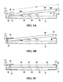
- FIGS. 6A, 6B and 6C are side elevation views illustrating the installation of an integrated circuit card into the holder of FIG. 1;
- FIG. 7 is a perspective view of the integrated circuit card holder of FIG. 1 mounted to a printed circuit board and holding an installed integrated circuit card;
- FIG. 8A, 8B and 8C are side elevation views of an alternative embodiment of the card holder showing installation of an integrated circuit card.
- a holder for an integrated circuit card comprising: a laterally extending non-conductive base; a pair of opposed abutments extending above the base, a first abutment of the pair of abutments being resilient such that a distance between the first abutment and a second abutment of the pair of abutments may be increased by urging the first abutment away from the second abutment; a first lip extending above the first abutment and projecting toward the second abutment; a second lip extending above or from the second abutment and projecting toward the first abutment; a plurality of resilient electrical contacts projecting upwardly from the base between the pair of abutments.
- a holder for an integrated circuit card comprising: a laterally extending non-conductive base; a pair of opposed abutments extending above said base, a first abutment of said pair of abutments being a resilient leaf spring such that a distance between said first abutment and a second abutment of said pair of abutments may be increased by urging said first abutment away from said second abutment; a first lip extending above said first abutment and projecting toward said second abutment; a second lip extending from an upper end of said second abutment and projecting toward said first abutment; a plurality of resilient electrical contacts projecting upwardly from said base between said pair of abutments; and stops for pre-loading said leaf spring positioned at opposite ends of said leaf spring, said stops being formed by a side of said first lip remote from said second lip, wherein said second abutment and said second lip have a first end portion
- the holder 10 is designed to hold an integrated circuit card of width W and thickness T.
- the holder 10 has a base 12 made from an electrically non-conductive material, such as plastic or glass-filled plastic.
- the central region 13 (FIG. 3) of the base is substantially flat.
- the base 12 has two ends 14 and 16. The base slopes downwardly at its ends 14 and 16 (see FIG. 3).
- a unitary, U-shaped bracket 24 is attached to end 14 of base 12.
- the bracket 24 may be formed from a metal such as stainless steel, copper or cold-rolled steel for example, e.g. by way of a stamping process.
- the bracket 24 may be attached to base 12 by injection molding of the plastic forming base 12 through holes 26 formed in the bracket 24 (see FIG. 2).
- the bracket 24 has an abutment 18 extending upwardly from the base 12, forming a right angle with the base and a lip 20 that extends towards the second end 16 of the base 12.
- the lip 20 forms a right angle with the abutment 18.
- the separation between the lip 20 and the central region 13 of base 12 is equal to T.
- the abutment 18 has a medial gap 22 (FIG. 1) that is wider than an average human finger which facilitates removal of the integrated circuit card from the holder 10.
- a notch 23 in base 12 is registered with the gap 22 and further facilitates card removal.
- an assembly 30 is attached to the base.
- the assembly has a generally U-shaped bracket with a central nose 35 which holds a resilient abutment 32.
- the attachment of bracket 34 to base 12 may also be through injection molding (e.g. bracket 24 and assembly 30 may be placed into a mold into which molten plastic forming base 12 is injected).
- the assembly 30 is shown in FIG. 4 prior to its attachment to base 12 and in FIGS. 1-3 after its attachment to base 12.
- the assembly 30 may be made from the same material as bracket 24.
- resilient abutment 32 is a leaf spring with two arms 40 and 42 that extend into cutout portions 50 and 52 of bracket 34, respectively.
- the arms 40 and 42 of spring 32 end in tabs 44 and 46 respectively.
- the distance between the opposing abutment 18 and tabs 44, 46 is slightly larger than W (denoted "W+" in FIGS. 1 and 2) in order to accommodate an integrated circuit card installed in holder 10.
- the leaf spring 32 is preloaded, i.e. partially compressed, with the arms 40 and 42 being partially flexed even when the holder 10 is empty.
- spring force presses tabs 44 and 46 against the outer edge of bracket 34 and the edge of base 12 (see, e.g., FIGS. 1 and 3, which act as stops).
- the preloading is not required, but may improve the ability of holder 10 to keep an installed integrated circuit card in position within the holder as compared to a non-preloaded spring.
- the spring 32 is capable of compression in a compression direction away from outer edge 37 and abutment 18 during integrated circuit card installation and removal. Resilient abutment 32 may be referred to as the "first abutment” while abutment 18 may be referred to as the "second abutment".
- Bracket 34 has a lip 36 that projects towards the abutment 18 at the first end 14 of base 12. Like lip 20, lip 36 is separated from the surface of base 12 by separation T+. Lip 36 may be referred to as the "first lip” while lip 20 may be referred to as the "second lip”.
- each of the contacts 60 is formed from one end of a thin strip 61 of electrically conductive material (such as a resilient metal), which end is bent into a convex shape, as shown in FIG. 5A.
- the strip 61 also has a basal end 62 and a neck 63 which extends between end 62 and contact 60. Neck 63 is received through an aperture 65 in base 12. When contact 60 is depressed, it produces an upward spring force.
- End 62 of each strip extends along the underside of the base 12 and beyond its margin. The ends 62 are intended for electrical connection to printed circuit board leads.
- FIG. 5B An alternative shape of metal strip 61 having a contact portion 60, basal end 62 and neck 63 is shown in FIG. 5B.
- the base 12 has an additional abutment 70 (FIG. 1) along one of its sides.
- the abutment 70 takes the form of an upstanding lip having a gap 72 therein.
- the gap results from a notch 74 of the base 12 into which the ends 62 of three contacts 60 extend.
- the notch 74 allows the ends 62 of the three contacts to extend beyond the margin of the base 12 of the holder without extending beyond the main footprint of the holder 10; this may conserve real estate on a printed circuit board onto which the holder 10 is mounted.
- FIGS. 6A to 6C Installation of a SIM card 80 into the holder 10 is illustrated in FIGS. 6A to 6C.
- a user initially holds the card 80 on an angle with respect to the base 12 as shown.
- the card is translated into the holder 10 towards assembly 30 until leading edge 82 of the card comes into contact with the tabs 44, 46 of leaf spring 32.
- Application of pressure upon the opposing card edge 84 towards spring 32 causes the spring 32 to compress.
- the spring 32 is compressed sufficiently for the opposing edge 84 to clear lip 20, as shown in FIG. 6B.
- the opposing edge 84 is then lowered past lip 20 towards the base 12 with spring compression being maintained.
- the edge 84 is then released.
- the spring 32 decompresses and urges the SIM card 80 into an installed position in which edge 84 of card 80 abuts the abutment 18, as shown in FIG. 6C.
- the tabs 44, 46 at the ends of the arms 40, 42 of spring 32 are returned to their original, preloaded position. In this position, the tabs 44, 46 are adjacent to the leading edge 82 of card 80 but are not continually applying pressure to the card 80. If the holder 10 is jarred such that SIM card 80 is driven into the preloaded leaf spring 32, the spring absorbs the shock of the jarring and returns the card 80 to its installed position as shown in FIG. 6C.
- contact pads 90 on its lower face are positioned directly over the contacts 60.
- the presence of SIM card 80 causes the contacts 60 to be downwardly depressed.
- the resiliency of the contacts 60 resists this depression and helps to maintain the contacts 60 in positive contact with the contact pads 90.
- the resiliency of contacts 60 also tends to press the SIM card 80 up against the first and second lips 36 and 20, which mechanically obstruct upward movement of the card 80. This helps to keep the card 80 in position within the holder 10.
- FIG. 7 is a perspective view of the holder 10 with an installed SIM card 80.
- the holder 10 is mounted to a printed circuit board 100, e.g. using conventional surface mount technology.
- the overall footprint of the holder 10 is approximately one-half of the footprint of the SIM card 80.
- the size of the holder may vary in relation to the size of the card in alternative embodiments.
- Stopper 102 is a form of abutment which may be a dedicated component (e.g. an upstanding tab as shown in FIG. 7) or a strategically placed component having another purpose beyond simply acting as a stopper, such as a shielding can used to shield an RF transmitter for example.
- the stopper 120 and lip 70 cooperate to keep the card 80 in place longitudinally (i.e. in direction D).
- Gap 22 may facilitate removal of the card 80 by providing an exposed portion of edge 84 for card manipulation.
- the upper surface of base 12 may be substantially flat, without downwardly sloping portions at ends 14 and 16.
- Such an alternative embodiment holder 110 is illustrated in FIGS. 8A to 8C.
- the separation between the lip 36 and base 12 is slightly larger than the thickness T of the integrated circuit card to be held to facilitate card installation.
- the separation between lip 20 and base 12 may similarly be slightly larger than T. Installation of an integrated circuit card 80 into the holder 110 is illustrated in FIGS. 8A to 8C.
- the distance between the opposing abutment 18 and tabs 44, 46 may be slightly less than W when the holder 10 is empty.
- the resilient abutment 32 continually applies pressure upon the edge 82 of an installed card 80. This may be sufficient to keep the card 80 in place for certain applications, even in the absence of lip 70 and stopper 102.
- lip 70 and stopper 102 are omitted, the risk of an intermittent electrical connection between the contacts 60 and pads 90 may increase due to possible movement of the card 80 in the longitudinal direction D.
- the end portions 62 of some or all of the wire strips 61 may not extend beyond a margin of the base. Rather, the ends 62 could be situated under the base 12 near its margin.
- the resilient abutment 32 may not be a leaf spring. Alternative embodiments may employ other types of springs or resilient abutments.
- Alternative embodiments may not be assembled from multiple components such as a bracket 24, an assembly 30 and a base 12. Rather, the holder may be integrally formed as a single workpiece. Moreover, resilient abutment 32 and bracket 34 are not necessarily parts of an assembly 30, but could be separate components.
- the contacts 60 are not necessarily made from a strip of metal 61 in all embodiments, but rather may be formed from wire, a conductive film, or another suitable material such as an electrically conductive elastomer.
- the contacts 60 are not necessarily resilient in all embodiments, however the likelihood of intermittent connections may increase if the contacts 60 are not resilient.
- the holder 10 can be used to hold various types of integrated circuit cards, not just SIM cards. These include Secure Digital (SD) memory cards, mini SD memory cards, micro SD memory cards and Sony ® Memory Stick TM cards for example.
- SD Secure Digital
- mini SD memory cards mini SD memory cards
- micro SD memory cards micro SD memory cards
- Sony ® Memory Stick TM cards for example.
Landscapes
- Engineering & Computer Science (AREA)
- Computer Networks & Wireless Communication (AREA)
- Signal Processing (AREA)
- Artificial Intelligence (AREA)
- Computer Vision & Pattern Recognition (AREA)
- Physics & Mathematics (AREA)
- General Physics & Mathematics (AREA)
- Theoretical Computer Science (AREA)
- Coupling Device And Connection With Printed Circuit (AREA)
- Telephone Set Structure (AREA)
- Credit Cards Or The Like (AREA)
Abstract
Description
- The present invention relates to an integrated circuit card holder, such as a Subscriber Identity Module (SIM) card holder.
- A SIM card is a smart card (a form of integrated circuit card) that is used with a Global System for Mobile Communications (GSM) cellular phone to encrypt voice and data transmissions and store user data permitting user identification and authentication on a network providing phone service. The SIM card also stores data such as the preferred phone settings of the user and a list of commonly dialled telephone numbers. A SIM card can be moved between telephones, and more than one SIM card can be used with one phone. For example, a cellular telephone with a first installed SIM card may be used for business calls, and the same telephone with a second installed SIM card may be used for personal calls.
- To facilitate the use of SIM cards as described above, many cellular telephones incorporate a SIM card holder that permit a SIM card to be easily installed without tools. For example, one known type of SIM card holder essentially consists of a rigid "pocket" that is mounted flat against a printed circuit board (PCB) within the telephone unit. A SIM card is inserted into the pocket with a sliding motion. The holder has elastic electrical contacts which come into contact with contact pads on the SIM card to form an electrical connection between the PCB and the inserted card. In certain holders of this type, about one half of the footprint (i.e. extent) of the inserted SIM card (the half with the contact pads) is within the holder when the card is inserted. The remaining half of the SIM card footprint extends beyond the holder and lies in a plane that is parallel to and slightly above the surface of the PCB. Below the extending half of the card, only low-profile components, e.g. resistors or capacitors that are no more than about 1 millimeter in height, are mounted to the PCB surface, to avoid mechanically obstructing the overlying SIM card.
- Use of the above-described type of SIM card holder may be problematic in that PCB components even beyond the footprint of the installed SIM card may need to be kept clear of the plane of the SIM card in order to facilitate card insertion and removal. For example, if the holder is centrally mounted on a PCB, it may be necessary to refrain from mounting high-profile components in area adjacent to the holder that is the same size as the entire SIM card footprint. This is so that the SIM card may be laid flat against the PCB surface in order to position it for insertion into the pocket. A PCB designer may be impeded from utilizing desired components in this adjacent area as a result.
- An alternative integrated circuit card holder which addresses the above-noted problem would be desirable.
- In the figures which illustrate an example embodiment of the invention:
- FIG. 1 is a perspective view of an integrated circuit card holder;
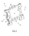
- FIG. 2 is a side elevation view of the integrated circuit card holder of FIG. 1;
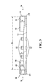
- FIG. 3 is a perspective view of the underside of the integrated circuit card holder of FIG. 1;
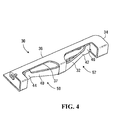
- FIG. 4 is perspective view of a component of the integrated circuit card holder of FIG. 1;
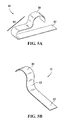
- FIG. 5A illustrates an electrical contact of the holder of FIG. 1 in greater detail;
- FIG. 5B illustrates an alternative form of electrical contact to the one shown in FIG. 5A;
- FIGS. 6A, 6B and 6C are side elevation views illustrating the installation of an integrated circuit card into the holder of FIG. 1;
- FIG. 7 is a perspective view of the integrated circuit card holder of FIG. 1 mounted to a printed circuit board and holding an installed integrated circuit card; and
- FIG. 8A, 8B and 8C are side elevation views of an alternative embodiment of the card holder showing installation of an integrated circuit card.
- In one aspect of the below-described embodiment, there is preferably provided a holder for an integrated circuit card comprising: a laterally extending non-conductive base; a pair of opposed abutments extending above the base, a first abutment of the pair of abutments being resilient such that a distance between the first abutment and a second abutment of the pair of abutments may be increased by urging the first abutment away from the second abutment; a first lip extending above the first abutment and projecting toward the second abutment; a second lip extending above or from the second abutment and projecting toward the first abutment; a plurality of resilient electrical contacts projecting upwardly from the base between the pair of abutments.
- In another aspect of the below-described embodiment there is preferably provided a holder for an integrated circuit card comprising: a laterally extending non-conductive base; a pair of opposed abutments extending above said base, a first abutment of said pair of abutments being a resilient leaf spring such that a distance between said first abutment and a second abutment of said pair of abutments may be increased by urging said first abutment away from said second abutment; a first lip extending above said first abutment and projecting toward said second abutment; a second lip extending from an upper end of said second abutment and projecting toward said first abutment; a plurality of resilient electrical contacts projecting upwardly from said base between said pair of abutments; and stops for pre-loading said leaf spring positioned at opposite ends of said leaf spring, said stops being formed by a side of said first lip remote from said second lip, wherein said second abutment and said second lip have a first end portion and a second end portion spaced by a medial gap, said base has a notch registered with said medial gap, and said base further has a central region that is substantially flat and downwardly sloping areas extending from said central region toward each of said pair of opposed abutments.
- Referring to FIGS. 1 - 4, an integrated
circuit card holder 10 is illustrated. Theholder 10 is designed to hold an integrated circuit card of width W and thickness T. Theholder 10 has abase 12 made from an electrically non-conductive material, such as plastic or glass-filled plastic. The central region 13 (FIG. 3) of the base is substantially flat. Thebase 12 has twoends ends 14 and 16 (see FIG. 3). - A unitary,
U-shaped bracket 24 is attached toend 14 ofbase 12. Thebracket 24 may be formed from a metal such as stainless steel, copper or cold-rolled steel for example, e.g. by way of a stamping process. Thebracket 24 may be attached tobase 12 by injection molding of theplastic forming base 12 throughholes 26 formed in the bracket 24 (see FIG. 2). Thebracket 24 has anabutment 18 extending upwardly from thebase 12, forming a right angle with the base and alip 20 that extends towards thesecond end 16 of thebase 12. Thelip 20 forms a right angle with theabutment 18. The separation between thelip 20 and the central region 13 ofbase 12 is equal to T. Due to the downward slope ofbase 12 atend 14, the separation between thelip 20 and the surface ofbase 12 is slightly larger than T (FIG. 6A). This separation, which is denoted "T+" in FIGS. 1 and 3, will accommodate an integrated circuit card during its installation intoholder 10. - The
abutment 18 has a medial gap 22 (FIG. 1) that is wider than an average human finger which facilitates removal of the integrated circuit card from theholder 10. Anotch 23 inbase 12 is registered with thegap 22 and further facilitates card removal. - At the
other end 16 ofbase 12, anassembly 30 is attached to the base. The assembly has a generally U-shaped bracket with acentral nose 35 which holds aresilient abutment 32. As withbracket 24, the attachment ofbracket 34 tobase 12 may also be through injection molding (e.g. bracket 24 andassembly 30 may be placed into a mold into which moltenplastic forming base 12 is injected). Theassembly 30 is shown in FIG. 4 prior to its attachment tobase 12 and in FIGS. 1-3 after its attachment tobase 12. Theassembly 30 may be made from the same material asbracket 24. - Referring to FIG. 1 along with FIG. 4,
resilient abutment 32 is a leaf spring with twoarms cutout portions bracket 34, respectively. Thearms spring 32 end intabs opposing abutment 18 andtabs holder 10. Theleaf spring 32 is preloaded, i.e. partially compressed, with thearms holder 10 is empty. In particular, spring force pressestabs bracket 34 and the edge of base 12 (see, e.g., FIGS. 1 and 3, which act as stops). The preloading is not required, but may improve the ability ofholder 10 to keep an installed integrated circuit card in position within the holder as compared to a non-preloaded spring. Thespring 32 is capable of compression in a compression direction away fromouter edge 37 andabutment 18 during integrated circuit card installation and removal.Resilient abutment 32 may be referred to as the "first abutment" whileabutment 18 may be referred to as the "second abutment". -
Bracket 34 has alip 36 that projects towards theabutment 18 at thefirst end 14 ofbase 12. Likelip 20,lip 36 is separated from the surface ofbase 12 by separation T+.Lip 36 may be referred to as the "first lip" whilelip 20 may be referred to as the "second lip". - As shown in FIG. 1, six
electrical contacts 60 are mounted in the base 12 in an arrangement that is suitable for contacting contact pads in the face of an installed SIM card. Each of thecontacts 60 is formed from one end of athin strip 61 of electrically conductive material (such as a resilient metal), which end is bent into a convex shape, as shown in FIG. 5A. Thestrip 61 also has abasal end 62 and aneck 63 which extends betweenend 62 andcontact 60.Neck 63 is received through an aperture 65 inbase 12. Whencontact 60 is depressed, it produces an upward spring force.End 62 of each strip extends along the underside of thebase 12 and beyond its margin. The ends 62 are intended for electrical connection to printed circuit board leads. - An alternative shape of
metal strip 61 having acontact portion 60,basal end 62 andneck 63 is shown in FIG. 5B. - Referring to FIG. 1, the
base 12 has an additional abutment 70 (FIG. 1) along one of its sides. Theabutment 70 takes the form of an upstanding lip having agap 72 therein. The gap results from anotch 74 of the base 12 into which the ends 62 of threecontacts 60 extend. Thenotch 74 allows theends 62 of the three contacts to extend beyond the margin of thebase 12 of the holder without extending beyond the main footprint of theholder 10; this may conserve real estate on a printed circuit board onto which theholder 10 is mounted. - Installation of a
SIM card 80 into theholder 10 is illustrated in FIGS. 6A to 6C. Referring to FIG. 6A, a user initially holds thecard 80 on an angle with respect to the base 12 as shown. The card is translated into theholder 10 towardsassembly 30 until leadingedge 82 of the card comes into contact with thetabs leaf spring 32. Application of pressure upon the opposingcard edge 84 towardsspring 32 causes thespring 32 to compress. Thespring 32 is compressed sufficiently for the opposingedge 84 toclear lip 20, as shown in FIG. 6B. The opposingedge 84 is then lowered pastlip 20 towards the base 12 with spring compression being maintained. - The
edge 84 is then released. Thespring 32 decompresses and urges theSIM card 80 into an installed position in whichedge 84 ofcard 80 abuts theabutment 18, as shown in FIG. 6C. Thetabs arms spring 32 are returned to their original, preloaded position. In this position, thetabs edge 82 ofcard 80 but are not continually applying pressure to thecard 80. If theholder 10 is jarred such thatSIM card 80 is driven into thepreloaded leaf spring 32, the spring absorbs the shock of the jarring and returns thecard 80 to its installed position as shown in FIG. 6C. - When the
SIM card 80 has been installed,contact pads 90 on its lower face are positioned directly over thecontacts 60. The presence ofSIM card 80 causes thecontacts 60 to be downwardly depressed. The resiliency of thecontacts 60 resists this depression and helps to maintain thecontacts 60 in positive contact with thecontact pads 90. The resiliency ofcontacts 60 also tends to press theSIM card 80 up against the first andsecond lips card 80. This helps to keep thecard 80 in position within theholder 10. - FIG. 7 is a perspective view of the
holder 10 with an installedSIM card 80. Theholder 10 is mounted to a printedcircuit board 100, e.g. using conventional surface mount technology. In the illustrated embodiment, the overall footprint of theholder 10 is approximately one-half of the footprint of theSIM card 80. The size of the holder may vary in relation to the size of the card in alternative embodiments. - One edge of
SIM card 80 abutsupstanding lip 70 and the opposing edge abuts astopper 102.Stopper 102 is a form of abutment which may be a dedicated component (e.g. an upstanding tab as shown in FIG. 7) or a strategically placed component having another purpose beyond simply acting as a stopper, such as a shielding can used to shield an RF transmitter for example. The stopper 120 andlip 70 cooperate to keep thecard 80 in place longitudinally (i.e. in direction D). - Given the manner of installation of
SIM card 80 intoholder 10 from above the holder, it is possible to situate high-profile components withinarea 104 of the printedcircuit board 100, adjacent to the installedcard 80, without impeding installation or removal ofcard 80. - To remove the
SIM card 80 fromholder 10, the installation procedure is reversed.Gap 22 may facilitate removal of thecard 80 by providing an exposed portion ofedge 84 for card manipulation. - As will be appreciated by those skilled in the art, modifications to the above-described embodiment can be made without departing from the essence of the invention.
- For example, in some embodiments the upper surface of
base 12 may be substantially flat, without downwardly sloping portions at ends 14 and 16. Such analternative embodiment holder 110 is illustrated in FIGS. 8A to 8C. In the illustrated embodiment, the separation between thelip 36 andbase 12 is slightly larger than the thickness T of the integrated circuit card to be held to facilitate card installation. The separation betweenlip 20 andbase 12 may similarly be slightly larger than T. Installation of anintegrated circuit card 80 into theholder 110 is illustrated in FIGS. 8A to 8C. - In some embodiments, the distance between the opposing
abutment 18 andtabs holder 10 is empty. In such embodiments, theresilient abutment 32 continually applies pressure upon theedge 82 of an installedcard 80. This may be sufficient to keep thecard 80 in place for certain applications, even in the absence oflip 70 andstopper 102. Of course, iflip 70 andstopper 102 are omitted, the risk of an intermittent electrical connection between thecontacts 60 andpads 90 may increase due to possible movement of thecard 80 in the longitudinal direction D. - In some embodiments, the
end portions 62 of some or all of the wire strips 61 may not extend beyond a margin of the base. Rather, the ends 62 could be situated under thebase 12 near its margin. - In some embodiments, the
resilient abutment 32 may not be a leaf spring. Alternative embodiments may employ other types of springs or resilient abutments. - Alternative embodiments may not be assembled from multiple components such as a
bracket 24, anassembly 30 and abase 12. Rather, the holder may be integrally formed as a single workpiece. Moreover,resilient abutment 32 andbracket 34 are not necessarily parts of anassembly 30, but could be separate components. - The
contacts 60 are not necessarily made from a strip ofmetal 61 in all embodiments, but rather may be formed from wire, a conductive film, or another suitable material such as an electrically conductive elastomer. Thecontacts 60 are not necessarily resilient in all embodiments, however the likelihood of intermittent connections may increase if thecontacts 60 are not resilient. - It will also be appreciated that the
holder 10 can be used to hold various types of integrated circuit cards, not just SIM cards. These include Secure Digital (SD) memory cards, mini SD memory cards, micro SD memory cards and Sony® Memory Stick™ cards for example. - Other modifications will be apparent to those skilled in the art and, therefore, the invention is defined in the claims.
Claims (16)
- A holder for an integrated circuit card comprising:a laterally extending non-conductive base;a pair of opposed abutments extending above said base, a first abutment of said pair of abutments being resilient such that a distance between said first abutment and a second abutment of said pair of abutments may be increased by urging said first abutment away from said second abutment;a first lip extending above said first abutment and projecting toward said second abutment;a second lip extending above or from said second abutment and projecting toward said first abutment;a plurality of resilient electrical contacts projecting upwardly from said base between said pair of abutments.
- The holder of claim 1 wherein each contact of said contacts has a first end portion projecting upwardly from said base, a neck extending through said base, and a second end portion extending below a lower surface of said base.
- The holder of claim 2 wherein said first end portion of said each contact has a convex configuration.
- The holder of claim 2 or claim 3 wherein said second end portion of said each contact extends beyond a margin of said base.
- The holder of any one of claims 2 to 4 wherein said base has a notch such that said second end portion of at least some of said plurality of contacts extends beyond a margin of said base at said notch.
- The holder of any preceding claim wherein said second lip extends from an upper end of said second abutment.
- The holder of any one of claims 1 to 5 wherein said second abutment and said second lip have a first end portion and a second end portion spaced by a medial gap.
- The holder of claim 7 wherein said base has a notch registered with said medial gap.
- The holder of any preceding claim wherein said first abutment is a leaf spring.
- The holder of claim 9 further comprising stops for pre-loading said leaf spring.
- The holder of claim 10 wherein said stops are positioned at opposite ends of said leaf spring and wherein said stops are formed by a side of said first lip remote from said second lip.
- The holder of claim 9 further comprising a first bracket, said first lip being formed on said first bracket, a medial portion of said first bracket holding a medial portion of said leaf spring, and marginal portions of said first bracket comprising said stops.
- The holder of any preceding claim wherein said holder is suitable for mounting to a substantially flat surface, and further comprising a first additional abutment extending above said base and a second additional abutment for mounting to said surface opposite said first additional abutment, said first and second additional abutments for limiting longitudinal integrated circuit card movement.
- The holder of claim 13 wherein said second additional abutment comprises an upstanding tab.
- The holder of any preceding claim wherein said base has a central region that is substantially flat and downwardly sloping areas extending from said central region toward each of said pair of opposed abutments.
- A cellular phone having a holder according to any one of claims 1 to 15.
Priority Applications (4)
| Application Number | Priority Date | Filing Date | Title |
|---|---|---|---|
| DE602006001648T DE602006001648D1 (en) | 2006-05-16 | 2006-05-16 | Card holder for IC card or SIM card |
| AT06114044T ATE400033T1 (en) | 2006-05-16 | 2006-05-16 | CARD HOLDER FOR IC CARD OR SIM CARD |
| EP06114044A EP1857959B1 (en) | 2006-05-16 | 2006-05-16 | Card holder for IC-card or SIM-card |
| CA2588481A CA2588481C (en) | 2006-05-16 | 2007-05-15 | Integrated circuit card holder |
Applications Claiming Priority (1)
| Application Number | Priority Date | Filing Date | Title |
|---|---|---|---|
| EP06114044A EP1857959B1 (en) | 2006-05-16 | 2006-05-16 | Card holder for IC-card or SIM-card |
Publications (2)
| Publication Number | Publication Date |
|---|---|
| EP1857959A1 true EP1857959A1 (en) | 2007-11-21 |
| EP1857959B1 EP1857959B1 (en) | 2008-07-02 |
Family
ID=36616852
Family Applications (1)
| Application Number | Title | Priority Date | Filing Date |
|---|---|---|---|
| EP06114044A Active EP1857959B1 (en) | 2006-05-16 | 2006-05-16 | Card holder for IC-card or SIM-card |
Country Status (4)
| Country | Link |
|---|---|
| EP (1) | EP1857959B1 (en) |
| AT (1) | ATE400033T1 (en) |
| CA (1) | CA2588481C (en) |
| DE (1) | DE602006001648D1 (en) |
Cited By (2)
| Publication number | Priority date | Publication date | Assignee | Title |
|---|---|---|---|---|
| EP2672421A1 (en) * | 2012-06-08 | 2013-12-11 | Sony Mobile Communications AB | A memory card holding device without movable parts |
| US20240040726A1 (en) * | 2022-07-29 | 2024-02-01 | Hewlett-Packard Development Company, L.P. | Locking card trays |
Citations (5)
| Publication number | Priority date | Publication date | Assignee | Title |
|---|---|---|---|---|
| DE10112259A1 (en) * | 2000-03-14 | 2001-09-27 | Sagem | Plug connection for chip cards |
| US20010032882A1 (en) * | 2000-02-24 | 2001-10-25 | Mitsubishi Electric Telecom Europe | Card reader and mobile equipment which has it |
| US20030022537A1 (en) * | 2000-02-18 | 2003-01-30 | Bricaud Herve Guy | Ergonomic electrical connector for a smart card |
| DE20215561U1 (en) * | 2002-06-07 | 2003-02-13 | Carry Computer Eng. Co., Ltd., Hsin Dian, Taipeh | card connectors |
| US20040198444A1 (en) * | 2002-08-02 | 2004-10-07 | Yen-Hung Chen | Mobile phone IC card holder |
-
2006
- 2006-05-16 DE DE602006001648T patent/DE602006001648D1/en active Active
- 2006-05-16 AT AT06114044T patent/ATE400033T1/en not_active IP Right Cessation
- 2006-05-16 EP EP06114044A patent/EP1857959B1/en active Active
-
2007
- 2007-05-15 CA CA2588481A patent/CA2588481C/en active Active
Patent Citations (5)
| Publication number | Priority date | Publication date | Assignee | Title |
|---|---|---|---|---|
| US20030022537A1 (en) * | 2000-02-18 | 2003-01-30 | Bricaud Herve Guy | Ergonomic electrical connector for a smart card |
| US20010032882A1 (en) * | 2000-02-24 | 2001-10-25 | Mitsubishi Electric Telecom Europe | Card reader and mobile equipment which has it |
| DE10112259A1 (en) * | 2000-03-14 | 2001-09-27 | Sagem | Plug connection for chip cards |
| DE20215561U1 (en) * | 2002-06-07 | 2003-02-13 | Carry Computer Eng. Co., Ltd., Hsin Dian, Taipeh | card connectors |
| US20040198444A1 (en) * | 2002-08-02 | 2004-10-07 | Yen-Hung Chen | Mobile phone IC card holder |
Cited By (3)
| Publication number | Priority date | Publication date | Assignee | Title |
|---|---|---|---|---|
| EP2672421A1 (en) * | 2012-06-08 | 2013-12-11 | Sony Mobile Communications AB | A memory card holding device without movable parts |
| US9311572B2 (en) | 2012-06-08 | 2016-04-12 | Sony Corporation | Card holding device |
| US20240040726A1 (en) * | 2022-07-29 | 2024-02-01 | Hewlett-Packard Development Company, L.P. | Locking card trays |
Also Published As
| Publication number | Publication date |
|---|---|
| ATE400033T1 (en) | 2008-07-15 |
| DE602006001648D1 (en) | 2008-08-14 |
| CA2588481A1 (en) | 2007-11-16 |
| EP1857959B1 (en) | 2008-07-02 |
| CA2588481C (en) | 2010-09-21 |
Similar Documents
| Publication | Publication Date | Title |
|---|---|---|
| US7422461B2 (en) | Integrated circuit card holder | |
| AU724143B2 (en) | Subscriber identity module (SIM) card holder | |
| JP3726215B2 (en) | Contact device for chip card device | |
| EP0926769A1 (en) | Very thin electrical connector for the connection of a smart card | |
| US9652639B2 (en) | Card holding member and card connector | |
| CN1183470C (en) | A subscriber identity module card holder | |
| EP1820278B1 (en) | Sim card retaining device | |
| US7161811B2 (en) | Card holder for SIM card | |
| US6409546B1 (en) | Card connector | |
| US6193557B1 (en) | Chip card connector | |
| EP1536365A2 (en) | Card holding structure for portable electronic device | |
| US7354290B2 (en) | Surface contact card holder | |
| CN100539310C (en) | Be used in the chip card contact device on SIM card or the usim card especially | |
| CA2588481C (en) | Integrated circuit card holder | |
| US20070087600A1 (en) | Surface contact card holder | |
| US20070131777A1 (en) | Chip card retaining mechanism | |
| US20050075138A1 (en) | Low profile electronic card holder and device using same | |
| CN109088202B (en) | Anti-crumple terminal, clamping seat and mobile equipment | |
| US20070093138A1 (en) | Electronic card connection devices | |
| KR100587305B1 (en) | Card connection device of mobile communication terminal | |
| KR101044095B1 (en) | Mobile terminal with bottom case grounded through card connector | |
| KR100949154B1 (en) | SIM card terminal of mobile phone | |
| US20090111291A1 (en) | Information storage card holding structure and electrical device using the same | |
| GB2364449A (en) | Connector for two SIM cards | |
| WO2007110100A1 (en) | Card reader with card ejection mechanism |
Legal Events
| Date | Code | Title | Description |
|---|---|---|---|
| PUAI | Public reference made under article 153(3) epc to a published international application that has entered the european phase |
Free format text: ORIGINAL CODE: 0009012 |
|
| 17P | Request for examination filed |
Effective date: 20060517 |
|
| AK | Designated contracting states |
Kind code of ref document: A1 Designated state(s): AT BE BG CH CY CZ DE DK EE ES FI FR GB GR HU IE IS IT LI LT LU LV MC NL PL PT RO SE SI SK TR |
|
| AX | Request for extension of the european patent |
Extension state: AL BA HR MK YU |
|
| GRAP | Despatch of communication of intention to grant a patent |
Free format text: ORIGINAL CODE: EPIDOSNIGR1 |
|
| GRAS | Grant fee paid |
Free format text: ORIGINAL CODE: EPIDOSNIGR3 |
|
| GRAA | (expected) grant |
Free format text: ORIGINAL CODE: 0009210 |
|
| AK | Designated contracting states |
Kind code of ref document: B1 Designated state(s): AT BE BG CH CY CZ DE DK EE ES FI FR GB GR HU IE IS IT LI LT LU LV MC NL PL PT RO SE SI SK TR |
|
| AX | Request for extension of the european patent |
Extension state: AL BA HR MK YU |
|
| REG | Reference to a national code |
Ref country code: GB Ref legal event code: FG4D |
|
| AKX | Designation fees paid |
Designated state(s): AT BE BG CH CY CZ DE DK EE ES FI FR GB GR HU IE IS IT LI LT LU LV MC NL PL PT RO SE SI SK TR |
|
| AXX | Extension fees paid |
Extension state: HR Payment date: 20060517 Extension state: AL Payment date: 20060517 Extension state: MK Payment date: 20060517 Extension state: YU Payment date: 20060517 Extension state: BA Payment date: 20060517 |
|
| REG | Reference to a national code |
Ref country code: CH Ref legal event code: EP |
|
| REF | Corresponds to: |
Ref document number: 602006001648 Country of ref document: DE Date of ref document: 20080814 Kind code of ref document: P |
|
| REG | Reference to a national code |
Ref country code: IE Ref legal event code: FG4D |
|
| PG25 | Lapsed in a contracting state [announced via postgrant information from national office to epo] |
Ref country code: SI Free format text: LAPSE BECAUSE OF FAILURE TO SUBMIT A TRANSLATION OF THE DESCRIPTION OR TO PAY THE FEE WITHIN THE PRESCRIBED TIME-LIMIT Effective date: 20080702 |
|
| PG25 | Lapsed in a contracting state [announced via postgrant information from national office to epo] |
Ref country code: NL Free format text: LAPSE BECAUSE OF FAILURE TO SUBMIT A TRANSLATION OF THE DESCRIPTION OR TO PAY THE FEE WITHIN THE PRESCRIBED TIME-LIMIT Effective date: 20080702 |
|
| NLV1 | Nl: lapsed or annulled due to failure to fulfill the requirements of art. 29p and 29m of the patents act | ||
| PG25 | Lapsed in a contracting state [announced via postgrant information from national office to epo] |
Ref country code: LT Free format text: LAPSE BECAUSE OF FAILURE TO SUBMIT A TRANSLATION OF THE DESCRIPTION OR TO PAY THE FEE WITHIN THE PRESCRIBED TIME-LIMIT Effective date: 20080702 Ref country code: IS Free format text: LAPSE BECAUSE OF FAILURE TO SUBMIT A TRANSLATION OF THE DESCRIPTION OR TO PAY THE FEE WITHIN THE PRESCRIBED TIME-LIMIT Effective date: 20081102 |
|
| PG25 | Lapsed in a contracting state [announced via postgrant information from national office to epo] |
Ref country code: ES Free format text: LAPSE BECAUSE OF FAILURE TO SUBMIT A TRANSLATION OF THE DESCRIPTION OR TO PAY THE FEE WITHIN THE PRESCRIBED TIME-LIMIT Effective date: 20081013 Ref country code: PT Free format text: LAPSE BECAUSE OF FAILURE TO SUBMIT A TRANSLATION OF THE DESCRIPTION OR TO PAY THE FEE WITHIN THE PRESCRIBED TIME-LIMIT Effective date: 20081202 Ref country code: LV Free format text: LAPSE BECAUSE OF FAILURE TO SUBMIT A TRANSLATION OF THE DESCRIPTION OR TO PAY THE FEE WITHIN THE PRESCRIBED TIME-LIMIT Effective date: 20080702 Ref country code: FI Free format text: LAPSE BECAUSE OF FAILURE TO SUBMIT A TRANSLATION OF THE DESCRIPTION OR TO PAY THE FEE WITHIN THE PRESCRIBED TIME-LIMIT Effective date: 20080702 Ref country code: BG Free format text: LAPSE BECAUSE OF FAILURE TO SUBMIT A TRANSLATION OF THE DESCRIPTION OR TO PAY THE FEE WITHIN THE PRESCRIBED TIME-LIMIT Effective date: 20081002 Ref country code: AT Free format text: LAPSE BECAUSE OF FAILURE TO SUBMIT A TRANSLATION OF THE DESCRIPTION OR TO PAY THE FEE WITHIN THE PRESCRIBED TIME-LIMIT Effective date: 20080702 |
|
| PG25 | Lapsed in a contracting state [announced via postgrant information from national office to epo] |
Ref country code: BE Free format text: LAPSE BECAUSE OF FAILURE TO SUBMIT A TRANSLATION OF THE DESCRIPTION OR TO PAY THE FEE WITHIN THE PRESCRIBED TIME-LIMIT Effective date: 20080702 |
|
| PG25 | Lapsed in a contracting state [announced via postgrant information from national office to epo] |
Ref country code: EE Free format text: LAPSE BECAUSE OF FAILURE TO SUBMIT A TRANSLATION OF THE DESCRIPTION OR TO PAY THE FEE WITHIN THE PRESCRIBED TIME-LIMIT Effective date: 20080702 Ref country code: DK Free format text: LAPSE BECAUSE OF FAILURE TO SUBMIT A TRANSLATION OF THE DESCRIPTION OR TO PAY THE FEE WITHIN THE PRESCRIBED TIME-LIMIT Effective date: 20080702 |
|
| PLBE | No opposition filed within time limit |
Free format text: ORIGINAL CODE: 0009261 |
|
| STAA | Information on the status of an ep patent application or granted ep patent |
Free format text: STATUS: NO OPPOSITION FILED WITHIN TIME LIMIT |
|
| PG25 | Lapsed in a contracting state [announced via postgrant information from national office to epo] |
Ref country code: SK Free format text: LAPSE BECAUSE OF FAILURE TO SUBMIT A TRANSLATION OF THE DESCRIPTION OR TO PAY THE FEE WITHIN THE PRESCRIBED TIME-LIMIT Effective date: 20080702 Ref country code: CZ Free format text: LAPSE BECAUSE OF FAILURE TO SUBMIT A TRANSLATION OF THE DESCRIPTION OR TO PAY THE FEE WITHIN THE PRESCRIBED TIME-LIMIT Effective date: 20080702 Ref country code: RO Free format text: LAPSE BECAUSE OF FAILURE TO SUBMIT A TRANSLATION OF THE DESCRIPTION OR TO PAY THE FEE WITHIN THE PRESCRIBED TIME-LIMIT Effective date: 20080702 |
|
| 26N | No opposition filed |
Effective date: 20090403 |
|
| PG25 | Lapsed in a contracting state [announced via postgrant information from national office to epo] |
Ref country code: IT Free format text: LAPSE BECAUSE OF FAILURE TO SUBMIT A TRANSLATION OF THE DESCRIPTION OR TO PAY THE FEE WITHIN THE PRESCRIBED TIME-LIMIT Effective date: 20080702 |
|
| PG25 | Lapsed in a contracting state [announced via postgrant information from national office to epo] |
Ref country code: MC Free format text: LAPSE BECAUSE OF NON-PAYMENT OF DUE FEES Effective date: 20090531 |
|
| PG25 | Lapsed in a contracting state [announced via postgrant information from national office to epo] |
Ref country code: SE Free format text: LAPSE BECAUSE OF FAILURE TO SUBMIT A TRANSLATION OF THE DESCRIPTION OR TO PAY THE FEE WITHIN THE PRESCRIBED TIME-LIMIT Effective date: 20081002 |
|
| PG25 | Lapsed in a contracting state [announced via postgrant information from national office to epo] |
Ref country code: IE Free format text: LAPSE BECAUSE OF NON-PAYMENT OF DUE FEES Effective date: 20090516 |
|
| PG25 | Lapsed in a contracting state [announced via postgrant information from national office to epo] |
Ref country code: PL Free format text: LAPSE BECAUSE OF FAILURE TO SUBMIT A TRANSLATION OF THE DESCRIPTION OR TO PAY THE FEE WITHIN THE PRESCRIBED TIME-LIMIT Effective date: 20080702 |
|
| PG25 | Lapsed in a contracting state [announced via postgrant information from national office to epo] |
Ref country code: GR Free format text: LAPSE BECAUSE OF FAILURE TO SUBMIT A TRANSLATION OF THE DESCRIPTION OR TO PAY THE FEE WITHIN THE PRESCRIBED TIME-LIMIT Effective date: 20081003 |
|
| REG | Reference to a national code |
Ref country code: CH Ref legal event code: PL |
|
| PG25 | Lapsed in a contracting state [announced via postgrant information from national office to epo] |
Ref country code: CH Free format text: LAPSE BECAUSE OF NON-PAYMENT OF DUE FEES Effective date: 20100531 Ref country code: LI Free format text: LAPSE BECAUSE OF NON-PAYMENT OF DUE FEES Effective date: 20100531 |
|
| PG25 | Lapsed in a contracting state [announced via postgrant information from national office to epo] |
Ref country code: LU Free format text: LAPSE BECAUSE OF NON-PAYMENT OF DUE FEES Effective date: 20090516 |
|
| PG25 | Lapsed in a contracting state [announced via postgrant information from national office to epo] |
Ref country code: HU Free format text: LAPSE BECAUSE OF FAILURE TO SUBMIT A TRANSLATION OF THE DESCRIPTION OR TO PAY THE FEE WITHIN THE PRESCRIBED TIME-LIMIT Effective date: 20090103 |
|
| PG25 | Lapsed in a contracting state [announced via postgrant information from national office to epo] |
Ref country code: TR Free format text: LAPSE BECAUSE OF FAILURE TO SUBMIT A TRANSLATION OF THE DESCRIPTION OR TO PAY THE FEE WITHIN THE PRESCRIBED TIME-LIMIT Effective date: 20080702 |
|
| PG25 | Lapsed in a contracting state [announced via postgrant information from national office to epo] |
Ref country code: CY Free format text: LAPSE BECAUSE OF FAILURE TO SUBMIT A TRANSLATION OF THE DESCRIPTION OR TO PAY THE FEE WITHIN THE PRESCRIBED TIME-LIMIT Effective date: 20080702 |
|
| REG | Reference to a national code |
Ref country code: DE Ref legal event code: R082 Ref document number: 602006001648 Country of ref document: DE Representative=s name: MERH-IP MATIAS ERNY REICHL HOFFMANN, DE |
|
| REG | Reference to a national code |
Ref country code: DE Ref legal event code: R082 Ref document number: 602006001648 Country of ref document: DE Representative=s name: MERH-IP MATIAS ERNY REICHL HOFFMANN, DE Effective date: 20140925 Ref country code: DE Ref legal event code: R081 Ref document number: 602006001648 Country of ref document: DE Owner name: BLACKBERRY LIMITED, WATERLOO, CA Free format text: FORMER OWNER: RESEARCH IN MOTION LTD., WATERLOO, ONTARIO, CA Effective date: 20140925 Ref country code: DE Ref legal event code: R082 Ref document number: 602006001648 Country of ref document: DE Representative=s name: MERH-IP MATIAS ERNY REICHL HOFFMANN PATENTANWA, DE Effective date: 20140925 |
|
| REG | Reference to a national code |
Ref country code: FR Ref legal event code: PLFP Year of fee payment: 11 |
|
| REG | Reference to a national code |
Ref country code: FR Ref legal event code: PLFP Year of fee payment: 12 |
|
| REG | Reference to a national code |
Ref country code: FR Ref legal event code: PLFP Year of fee payment: 13 |
|
| REG | Reference to a national code |
Ref country code: DE Ref legal event code: R082 Ref document number: 602006001648 Country of ref document: DE Ref country code: DE Ref legal event code: R081 Ref document number: 602006001648 Country of ref document: DE Owner name: MALIKIE INNOVATIONS LTD., IE Free format text: FORMER OWNER: BLACKBERRY LIMITED, WATERLOO, ONTARIO, CA |
|
| PGFP | Annual fee paid to national office [announced via postgrant information from national office to epo] |
Ref country code: DE Payment date: 20250528 Year of fee payment: 20 |
|
| PGFP | Annual fee paid to national office [announced via postgrant information from national office to epo] |
Ref country code: GB Payment date: 20250520 Year of fee payment: 20 |
|
| PGFP | Annual fee paid to national office [announced via postgrant information from national office to epo] |
Ref country code: FR Payment date: 20250526 Year of fee payment: 20 |