EP1855361A2 - Connector mounting structure - Google Patents
Connector mounting structure Download PDFInfo
- Publication number
- EP1855361A2 EP1855361A2 EP07008795A EP07008795A EP1855361A2 EP 1855361 A2 EP1855361 A2 EP 1855361A2 EP 07008795 A EP07008795 A EP 07008795A EP 07008795 A EP07008795 A EP 07008795A EP 1855361 A2 EP1855361 A2 EP 1855361A2
- Authority
- EP
- European Patent Office
- Prior art keywords
- body member
- mounting structure
- connector
- structure according
- connector mounting
- Prior art date
- Legal status (The legal status is an assumption and is not a legal conclusion. Google has not performed a legal analysis and makes no representation as to the accuracy of the status listed.)
- Granted
Links
Images



Classifications
-
- H—ELECTRICITY
- H01—ELECTRIC ELEMENTS
- H01R—ELECTRICALLY-CONDUCTIVE CONNECTIONS; STRUCTURAL ASSOCIATIONS OF A PLURALITY OF MUTUALLY-INSULATED ELECTRICAL CONNECTING ELEMENTS; COUPLING DEVICES; CURRENT COLLECTORS
- H01R13/00—Details of coupling devices of the kinds covered by groups H01R12/70 or H01R24/00 - H01R33/00
- H01R13/46—Bases; Cases
- H01R13/502—Bases; Cases composed of different pieces
- H01R13/506—Bases; Cases composed of different pieces assembled by snap action of the parts
-
- H—ELECTRICITY
- H01—ELECTRIC ELEMENTS
- H01R—ELECTRICALLY-CONDUCTIVE CONNECTIONS; STRUCTURAL ASSOCIATIONS OF A PLURALITY OF MUTUALLY-INSULATED ELECTRICAL CONNECTING ELEMENTS; COUPLING DEVICES; CURRENT COLLECTORS
- H01R12/00—Structural associations of a plurality of mutually-insulated electrical connecting elements, specially adapted for printed circuits, e.g. printed circuit boards [PCB], flat or ribbon cables, or like generally planar structures, e.g. terminal strips, terminal blocks; Coupling devices specially adapted for printed circuits, flat or ribbon cables, or like generally planar structures; Terminals specially adapted for contact with, or insertion into, printed circuits, flat or ribbon cables, or like generally planar structures
- H01R12/50—Fixed connections
- H01R12/51—Fixed connections for rigid printed circuits or like structures
- H01R12/55—Fixed connections for rigid printed circuits or like structures characterised by the terminals
- H01R12/57—Fixed connections for rigid printed circuits or like structures characterised by the terminals surface mounting terminals
-
- H—ELECTRICITY
- H01—ELECTRIC ELEMENTS
- H01R—ELECTRICALLY-CONDUCTIVE CONNECTIONS; STRUCTURAL ASSOCIATIONS OF A PLURALITY OF MUTUALLY-INSULATED ELECTRICAL CONNECTING ELEMENTS; COUPLING DEVICES; CURRENT COLLECTORS
- H01R13/00—Details of coupling devices of the kinds covered by groups H01R12/70 or H01R24/00 - H01R33/00
- H01R13/46—Bases; Cases
- H01R13/52—Dustproof, splashproof, drip-proof, waterproof, or flameproof cases
- H01R13/521—Sealing between contact members and housing, e.g. sealing insert
-
- H—ELECTRICITY
- H01—ELECTRIC ELEMENTS
- H01R—ELECTRICALLY-CONDUCTIVE CONNECTIONS; STRUCTURAL ASSOCIATIONS OF A PLURALITY OF MUTUALLY-INSULATED ELECTRICAL CONNECTING ELEMENTS; COUPLING DEVICES; CURRENT COLLECTORS
- H01R12/00—Structural associations of a plurality of mutually-insulated electrical connecting elements, specially adapted for printed circuits, e.g. printed circuit boards [PCB], flat or ribbon cables, or like generally planar structures, e.g. terminal strips, terminal blocks; Coupling devices specially adapted for printed circuits, flat or ribbon cables, or like generally planar structures; Terminals specially adapted for contact with, or insertion into, printed circuits, flat or ribbon cables, or like generally planar structures
- H01R12/70—Coupling devices
- H01R12/7005—Guiding, mounting, polarizing or locking means; Extractors
- H01R12/7011—Locking or fixing a connector to a PCB
- H01R12/707—Soldering or welding
-
- H—ELECTRICITY
- H01—ELECTRIC ELEMENTS
- H01R—ELECTRICALLY-CONDUCTIVE CONNECTIONS; STRUCTURAL ASSOCIATIONS OF A PLURALITY OF MUTUALLY-INSULATED ELECTRICAL CONNECTING ELEMENTS; COUPLING DEVICES; CURRENT COLLECTORS
- H01R12/00—Structural associations of a plurality of mutually-insulated electrical connecting elements, specially adapted for printed circuits, e.g. printed circuit boards [PCB], flat or ribbon cables, or like generally planar structures, e.g. terminal strips, terminal blocks; Coupling devices specially adapted for printed circuits, flat or ribbon cables, or like generally planar structures; Terminals specially adapted for contact with, or insertion into, printed circuits, flat or ribbon cables, or like generally planar structures
- H01R12/70—Coupling devices
- H01R12/71—Coupling devices for rigid printing circuits or like structures
- H01R12/712—Coupling devices for rigid printing circuits or like structures co-operating with the surface of the printed circuit or with a coupling device exclusively provided on the surface of the printed circuit
- H01R12/714—Coupling devices for rigid printing circuits or like structures co-operating with the surface of the printed circuit or with a coupling device exclusively provided on the surface of the printed circuit with contacts abutting directly the printed circuit; Button contacts therefore provided on the printed circuit
-
- H—ELECTRICITY
- H01—ELECTRIC ELEMENTS
- H01R—ELECTRICALLY-CONDUCTIVE CONNECTIONS; STRUCTURAL ASSOCIATIONS OF A PLURALITY OF MUTUALLY-INSULATED ELECTRICAL CONNECTING ELEMENTS; COUPLING DEVICES; CURRENT COLLECTORS
- H01R13/00—Details of coupling devices of the kinds covered by groups H01R12/70 or H01R24/00 - H01R33/00
- H01R13/46—Bases; Cases
- H01R13/52—Dustproof, splashproof, drip-proof, waterproof, or flameproof cases
- H01R13/5202—Sealing means between parts of housing or between housing part and a wall, e.g. sealing rings
-
- H—ELECTRICITY
- H01—ELECTRIC ELEMENTS
- H01R—ELECTRICALLY-CONDUCTIVE CONNECTIONS; STRUCTURAL ASSOCIATIONS OF A PLURALITY OF MUTUALLY-INSULATED ELECTRICAL CONNECTING ELEMENTS; COUPLING DEVICES; CURRENT COLLECTORS
- H01R13/00—Details of coupling devices of the kinds covered by groups H01R12/70 or H01R24/00 - H01R33/00
- H01R13/73—Means for mounting coupling parts to apparatus or structures, e.g. to a wall
- H01R13/74—Means for mounting coupling parts in openings of a panel
Definitions
- the present invention relates to a connector mounting structure in which a male connector is surface-mounted to a circuit board.
- a connector mounting structure for mounting a male connector to a circuit board is disclosed in, for example, US 6,866,524 corresponding to JP-A-2004-206924 .
- connector terminals extending from a connector housing are electrically connected (i.e., surface-mounted) to conductive lands formed on a mounting surface of a circuit board by reflow soldering to achieve high circuit density, miniaturization, and efficient manufacturing process.
- the connector terminals have first end portions exposed to a first side of the connector housing and soldered to the circuit board and have second end portions exposed to a second side opposite to the first side to be connectable to a female connector.
- the first and second end portions are exposed to the different sides of the connector housing. Therefore, as the number of the connector terminals (i.e., circuit density) is increased, the connector housing is longitudinally elongated so that the size of the circuit board is increased in a direction along the mounting surface. Accordingly, the size of an electronic apparatus employing the circuit board is increased. If the first and second end portions are exposed to the same side of the connector housing, the number of the terminals may be increased without increasing the size of the electronic apparatus.
- the first and second end portions are exposed to the same side of the connector housing, the first end portions need to be soldered to the circuit board through inside the connector housing in view of the fact that temperature becomes high in the reflow soldering. Therefore, the connector housing needs to be placed on the circuit board, and the mounting surface is reduced accordingly. The size of the circuit board cannot be reduced, and the size of the electronic apparatus cannot be reduced.
- short-circuit between adjacent first end portions may be caused by a conductive foreign matter that falls on the first end portions before the male connector is mated with the female connector.
- the short-circuit may be caused by the foreign matter that sticks to the female connector and falls on the first end portions after the male connector is mated with the female connector.
- the connector housing is assembled as one piece from separate pieces to reduce the size of a circuit board, i.e., to increase circuit density of the circuit board.
- the short circuit cause by the foreign matter is not taken into consideration.
- the connector mounting structure includes a circuit board and a male connector capable of being mated with an external female connector.
- the male connector is surface-mounted to a mounting surface of the circuit board and has a connector housing and a plurality of male terminals.
- the connector housing includes a body member and a fixing member fixed to the body member.
- the body member has a surface
- the fixing member has a tube portion and a protection portion.
- the tube portion receives a connector housing of the female connector, when the male connector is mated with the female connector.
- Each of the male terminals is fixed in the body member and has first and second end portions and a joint portion.
- the first end portion is exposed to the surface of the body member and electrically connected to the circuit board.
- the second end portion is also exposed to the surface of the body member and placed above the first end portion in a thickness direction of the circuit board to be electrically connectable to the female connector.
- the joint portion connects the first and second end portions and is fixed in the body member.
- the protection portion is placed between the first and second end portions in the thickness direction of the circuit board to cover facing area between adjacent first end portions.
- both the first and second end portions of each of the male terminals are exposed to the same surface of the body member.
- the body member and the fixing member of the connector housing are separate pieces.
- the connector housing is assembled as one piece from the body member and the fixing member in such a manner that the body member is at least partially placed in the tube portion of the fixing member.
- the circuit board can be reduced in size in a direction along the mounting surface.
- the protection portion covers the facing area between the adjacent first end portions to prevent a foreign matter from touching the adjacent first end portions at one time. In such an approach, short-circuit caused by the foreign matter can be reduced without increasing the size of the circuit board.
- an electronic apparatus 100 includes a circuit board 200, a male connector 300 surface-mounted to the circuit board 200, and a casing 400 for housing the circuit board 200.
- the male connector 300 has a connector mounting structure according to a first embodiment of the present invention.
- a sealant 500 seals the electronic apparatus 100 so that an inner space S of the electronic apparatus 100 is waterproofed, i.e., protected from water damage.
- the electronic apparatus 100 may be suitable for an engine electronic control unit (ECU) installed in an engine room, which is located on the exterior of a vehicle.
- ECU engine electronic control unit
- the circuit board 200 includes a printed board 210 and electronic devices mounted to the printed board 210.
- the electronic devices are a microcomputer, a resistor, a capacitor, and the like, which are not shown in the drawings.
- the male connector 300 is one example of the electronic devices.
- the printed board 210 is provided with conductive patterns and via holes for connecting the conductive patterns.
- the printed board 210 is made of a known material such as a thermoplastic resin, a thermoset resin, a ceramic, or a glass/resin composite material (e.g., glass-cloth).
- the printed board 210 is a multilayered board that uses a FR-5-equivalent board made of a glass/epoxy-resin composite material and has a multi-layered conductive pattern.
- the male connector 300 includes a connector housing 320 and a plurality of first terminals 310a mounted in the connector housing 320.
- Each first terminal 310a is made of an electrically conductive material such as a metal plated brass.
- the connector housing 320 is made of an electrically insulating material such as a synthetic resin.
- the male connector 300 is mounted to the circuit board 200 and acts as an input/output interface of the circuit board 200.
- the connector housing 320 includes a body member 330 and a fixing member 340.
- the body member 330 and the fixing member 340 are separate pieces.
- Each of the first terminals 310a is mounted to the body member 330.
- the fixing member 340 has first, second, and third fixing portion 341-343.
- the first, second, and third fixing portions 341-343 are used to fix the fixing member 340 to, an external female connector to be mated with the male connector 300, the casing 400 via the sealant 500, and the body member 330, respectively.
- At least the first fixing portion 341 is shaped like a tube to receive a connector housing of the female connector.
- each of the first terminals 310a has a first end portion 311 a, a second end portion 312a, and a joint portion 313a.
- the first end portion 311 a is exposed to a first longitudinal surface 331 of the body member 330 and soldered to a conductive land formed on a mounting surface of the printed board 210.
- the second end portion 312a is also exposed to the first longitudinal surface 331 of the body member 330 to be electrically connectable to the female connector. Therefore, the first end portion 311 a and the second end portion 312a extend to the same side with respect to the body member 330.
- the joint portion 313a connects the first end portion 311 a and the second end portion 312a so that the first terminal 310a is approximately C-shaped.
- the first end portion 311 a is positioned below the second end portion 312a in a thickness direction of the circuit board 200 in a condition where the first terminal 310a is mounted to the circuit board 200 (i.e., the first end portion 311a is soldered to the conductive land formed on the mounting surface of the circuit board 200).
- the body member 330 is shaped like an approximately rectangular solid and has the first longitudinal surface 331.
- the first longitudinal surface 331 of the body member 330 is approximately perpendicular to the mounting surface of the circuit board 200.
- each of the first and second end portions 311a, 312a is exposed to and extends from the first longitudinal surface 331.
- the first terminals 310a are arranged in a longitudinal direction of the body member 330.
- the body member 330 has a plurality of slits 332 on the first longitudinal surface 331.
- the joint portion 313a of the first terminal 310a is placed and fixed in a corresponding one of the slits 332.
- Each slit 332 has a depth enough to fully accommodate the joint portion 313a so that the joint portion 313a is not exposed to the first longitudinal surface 331. Therefore, short-circuit caused by a conductive foreign matter 600 between adjacent joint portions 313a can be reduced.
- an engagement portion 333 is integrally provided on each of side surfaces, adjacent to the first longitudinal surface 331, and a top surface of the body member 330.
- the body member 330 and the fixing member 340 are fixed together by the engagement portion 333.
- the fixing member 340 has a tube portion at least at the first fixing portion 341, as shown in FIG. 3A.
- the connector housing of the female connector is received in the tube portion of the fixing member 340 so that the male connector 300 can be mated with the female connector.
- the first, second, and third fixing portions 341-343 of the fixing member 340 are arranged in that order from an open side of the tube portion where the male connector 300 is mated with the female connector.
- First and second projections 344, 345 which are spaced from each other, are provided on an outer surface of the tube portion of the fixing member 340.
- the first fixing portion 341 extends from the opening of the tube portion to an edge of the second projection 345. Therefore, the first fixing portion 341 includes the first projection 344 and a first recess between the first and second projections 344, 345, and does not include the second projection portion 345.
- the first projection 344 can be received in a receiver of the connector housing of the female connector.
- the second fixing portion 342 includes the second projection 345 and a second recess. The first and second recesses are opposite to each other across the second projection 345.
- the sealant 500 is disposed in the second recess, and an opening edge 430 of a connector opening of the casing 400 is attached to the second recess through the sealant 500.
- the rest of the fixing member 340 is the third fixing portion 343.
- a slit 346 for receiving the engagement portion 333 of the body member 330 is provided on an inner surface of the third fixing portion 343 of the fixing member 340.
- a guiding slit 349 for receiving both sides of the circuit board 200 is provided on an inner surface of the fixing member 340 (specifically, the second and third fixing portions 342, 343).
- the circuit board 200 can be positioned with respect to the fixing member 340 by inserting both sides of the circuit board 200 into the guiding slit 349.
- the guiding slit 349 has a predetermined length and extends in a longitudinal direction of the fixing member 340 from an opposite side to the open side of the tube portion.
- the guiding slit 349 has a uniform width equal to or slightly larger than a thickness of the printed board 210.
- the connector housing 320 of the male connector 300 is assembled as one piece from the separate pieces, i.e., the body member 330 and the fixing member 340. Therefore, the male connector 300 can be easily and reliably mounted to the circuit board 200 as follows.
- the body member 330 is mounted to the circuit board 200 by reflow soldering. Specifically, the first end portion 311a exposed to the first longitudinal surface 331 of the body member 330 is soldered to the conductive land formed on the printed board 200.
- the circuit board 200 is positioned with respect to the fixing member 340 by using the guiding slit 349.
- the male connector 300 is mounted to the circuit board 200 by using the connector mounting structure according to the first embodiment.
- the fixing member 340 includes first and second protection portions 347, 348, each of which is unitary with the fixing member 340 and made of the same material as the fixing member 340.
- the first protection portion 347 projects from a bottom inner surface of the tube portion of the fixing member 340. In the condition where the body member 330 and the fixing member 340 are fixed together, the first protection portion 347 is placed between the first and second end portions 311 a, 312a in the thickness direction of the circuit board 200 and touches the first longitudinal surface 331 of the body member 330.
- the first protection portion 347 covers at least a first facing area between adjacent first end portions 311 a without touching the adjacent first end portions 311 a. Thus, it is unlikely one foreign matter 600 touches both the adjacent first end portions 311 a at the same time. Thus, short-circuit caused by the foreign matter 600 between the adjacent first end portions 311 a can be reduced.
- the first protection portion 347 extends from a first point further away from the first longitudinal surface 331 of the body member 330 than a second point to which the first end portion 311 a extends.
- the first protection portion 347 has a slope portion so that a gap between the first protection portion 347 and the mounting surface of the circuit board 200 decreases with distance from the body member 330.
- the foreign matter 600 rolls or slides down the first protection portion 347 away from the body member 330, as shown in FIG.1A.
- the short-circuit caused by the foreign matter 600 between adjacent second end portions 312a can be reduced.
- the second protection portion 348 projects from a top inner surface of the fixing member 340. In the condition where the body member 330 and the fixing member 340 are fixed together, the second protection portion 348 touches an edge portion of the first longitudinal surface 331 of the body member 330. The second protection portion 348 prevents the foreign matter 600 from entering the inner space S of the casing 400 via a clearance between the body member 330 and the fixing member 340. The second protection portion 348 reduces or complicates the clearance, i.e., a passage to the inner space S. Preferably, the second protection portion 348 seals the clearance. In the first embodiment, the second protection portion 348 projects inwardly from the inner surface of the third fixing portion 343 of the fixing member 340, as shown in FIG. 3A.
- the casing 400 is made of synthetic resin or metal such as aluminum or iron.
- the casing 400 includes a case 410 shaped like a box with an opening and a cover 420 shaped like a rectangular plate.
- the cover 420 is attached to the case 410 by a screw, for example.
- the opening of the case 410 is covered with the cover 420 to produce the inner space S of the casing 400.
- the casing 400 is constructed from two pieces, i.e., the case 410 and the cover 420.
- the casing 400 may be a single piece or constructed from three or more pieces.
- the circuit board 200 is sandwiched between the case 410 and the cover 420 through an elastic member 510 such as a rubber. Thus, the circuit board 200 is fixed to the casing 400.
- the casing 400 has the connector opening for receiving the male connector 300. Due to the connector opening, the second end portion 312a of the first terminal 310a of the male connector 300 is exposed outside the casing 400 in a condition where the circuit board 200 is housed in the casing 400. Thus, the circuit board 200 can be electrically connected to the female connector through the male connector 300. As described above, in the first embodiment, the sealant 500 is placed between the opening edge 430 of the connector opening of the casing 400 and the second fixing portion 342 of the fixing member 340.
- the sealant 500 is made of a material having elasticity and adhesion enough to seal the casing 400.
- the inner space S of the casing 400 is protected from the water damage in a condition where the male connector 300 is mated with the female connector.
- the sealant 500 is moisture curing silicone adhesive having hardness (i.e., viscosity) of between 150 pascal-second (Pa ⁇ s) and 200 Pa ⁇ s before the adhesive cures.
- the sealant 500 may be a material disclosed in JP-2005-93602 related to the invention of the present applicants.
- the male connector 300 includes the first terminal 310a having the first and second end portions 311a, 312a. Each of the first and second end portions 311a, 312a is exposed to and extends from the first longitudinal surface 331 of the body member 330.
- the connector housing 320 of the male connector 300 is assembled as one piece from the separate pieces, i.e., the body member 330 and the fixing member 340. In the condition where the body member 330 is mounted to the circuit board 200 by the reflow soldering, the body member 330 and the fixing member 340 are fixed together. In such an approach, the circuit board 200 can be reduced in size in the direction along the mounting surface.
- the fixing member 340 has the first protection portion 347.
- the first protection portion 347 is placed between the first and second end portions 311a, 312a in the thickness direction of the circuit board 200 to cover at least the facing area between adjacent first end portions 311a.
- the circuit board 200 can be reduced in size in the direction along the mounting surface without increasing the possibility of the short-circuit caused by the foreign matter 600.
- the fixing member 340 further has the second protection portion 348.
- the second protection portion 348 touches the edge portion of the first longitudinal surface 331 to seal the clearance between the body member 330 and the fixing member 340.
- the second protection portion 348 prevents the foreign matter 600 from entering the inner space S of the casing 400 via the clearance between the body member 330 and the fixing member 340.
- the first protection portion 347 extends from the first point further away from the first longitudinal surface 331 than the second point to which the first end portion 311a extends. In such an approach, the short-circuit between the adjacent first end portions 311a can be surely prevented.
- the first protection portion 347 may be provided as shown in FIGS. 4A and 4B, where the first protection portion 347 covers only the facing area between the adjacent first end portions 311a.
- the first protection portion 347 has the slope portion so that the gap between the first protection portion 347 and the mounting surface of the circuit board 200 decreases with the distance from the body member 330.
- the first protection portion 347 may not have the slope portion. In this case, the gap between the first protection portion 347 and the second end portion 312a needs to be increased.
- the first protection portion 347 touches the first longitudinal surface 331 of the body member 330 to prevent the foreign matter 600 from entering the first facing area between the adjacent first end portions 311 a via a clearance between the first protection portion 347 and the first longitudinal surface 331.
- the short-circuit caused by the foreign matter 600 between the adjacent first end portions 311a can be surely reduced.
- the first protection portion 347 does not touch the first longitudinal surface 331. Therefore, the clearance between the first protection portion 347 and the first longitudinal surface 331 needs to be sealed with something.
- the first protection portion 347 is unitary with the fixing member 340.
- structure of the male connector 300 can be simplified so that manufacturing steps can be reduced.
- the first protection portion 347 may be separated from the fixing member 340.
- an electrically insulating material (e.g., protective gel) coating on the first end portion 311 a serves as the first protection portion 347.
- the first protection portion 347 When the first protection portion 347 is made of the electrically insulating material, it is preferable that the first protection portion 347 should be placed as close to the first end portion 311 a as possible, as in the case of FIG. 5. In such an approach, gap between the first protection portion 347 and the second end portion 312a is increased so that the short-circuit caused by the foreign matter 600 between the adjacent second end portions 312a can be reduced. It is more preferable that the first protection portion 347 should touch the first end portion 311a, as in the case of FIG. 6.
- the joint portion 313a of the first terminal 310a is placed in the slit 332 and fixed inside the body member 330.
- the slit 332 has the depth enough to fully accommodate the joint portion 313a so that the joint portion 313a is not exposed to the first longitudinal surface 331, i.e., a whole portion of the joint portion 313a is placed in the slit 332.
- the short-circuit caused by the foreign matter 600 between the adjacent joint portions 313a is reduced by adjusting the depth of the slit 332.
- the fixing member 340 has a third protection portion 350 and does not have the second protection portion 348.
- the third protection portion 350 is provided in front of the first longitudinal surface 331 of the body member 330 to cover at least the joint portion 313a and a second facing area between the adjacent joint portions 313a in the condition where the body member 330 and the fixing member 340 are fixed together.
- the short-circuit caused by the foreign matter 600 between the adjacent joint portions 313a can be reduced by the third protection portion 350.
- a contact portion of the second end portion 312a is electrically connected to the female connector. At least the contact portion of the second end portion 312a is placed further forward than the third protection portion 350 with respect to the first longitudinal surface 331 of the body member 330. Thus, although the third protection portion 350 is provided in front of the first longitudinal surface 331, the second end portion 312a can be electrically connected to the female connector.
- the joint portion 313a is placed in the slit 332, a portion of the joint portion 313a is exposed as shown in FIG. 2C.
- the third protection portion 350 covers both the joint portion 313a and the second facing area between the adjacent joint portions 313a.
- the third protection portion 350 is unitary with the fixing member 340 and made of the same material as the fixing member 340.
- the third protection portion 350 is also unitary with the first protection portion 347.
- the structure of the male connector 300 can be simplified so that the manufacturing steps can be reduced.
- the third protection portion 350 unitary with the first protection portion 347 is provided in front of the first longitudinal surface 331 to block the tube portion of the fixing member 340 to pass through between the second end portions 312a of the first terminal 310a.
- the third protection portion 350 seals the clearance between the body member 330 and the fixing member 340.
- the third protection portion 350 can serve as the second protection portion 348 and prevent the foreign matter 600 from entering the inner space S of the casing 400 via the clearance.
- the first protection portion 347 has the slope portion.
- the third protection portion 350 includes a base portion 351 and hole portions 352 defined by inner walls 353 of the base portion 351.
- the base portion 351 is placed approximately parallel to the first longitudinal surface 331.
- Each second end portion 312a is inserted through a corresponding one of the hole portions 352.
- the third protection portion 350 should be placed as close to the first longitudinal surface 331 as possible to reduce the length of the second end portion 312a, i.e., to reduce the size of the electronic apparatus 100. It is more preferable that the third protection portion 350 should touch the first longitudinal surface 331.
- the third protection portion 350 is placed as close to the first longitudinal surface 331 as possible with space in the condition where the body member 330 and the fixing member 340 are fixed together.
- each hole portion 352 is a through hole that penetrates the base portion 351.
- the diameter of the hole portion 352 on the side where the male connector 300 is mated with the female connector is slightly larger than the diameter of the second end portion 312a.
- the hole portion 352 is tapered so that the diameter of the hole portion 352 is larger on the body member 330 side than on the side where the male connector 300 is mated with the female connector.
- each inner wall 353 of the hole portion 352 acts as a guiding member for guiding the second end portion 312a through the hole portion 352.
- the first terminal 310a can be positioned with respect to the body member 330 by inserting the second end portion 312a through the hole portion 352 of the third protection portion 350.
- the second end portion 312a can be easily inserted though the hole portion 352 without hitting against the base portion 351. Therefore, stress caused by the hit on junction between the first end portion 311a and the circuit board 200 can be reduced so that connection reliability between the first end portion 311a and the circuit board 200 can be ensured.
- the second end portion 312a except the contact portion has a projection 314a extending toward the body member 330.
- the projection 314a is placed further forward than the third protection portion 350 with respect to the first longitudinal surface 331 of the body member 330. Therefore, the contact portion of the second end portion 312a can be electrically connected to the female connector. Even when stress in a direction opposite to the insertion direction of the second end portion 312a is applied to the second end portion 312a in the condition where the body member 330 and the fixing member 340 are fixed together, the projection 314a of the second end portion 312a catches the third protection portion 350 to ensure the electrical connection between the second end portion 312a and the female connector. Thus, the male connector 300 can be reliably mated with the female connector.
- the third protection portion 350 is unitary with the first protection portion 347 and is provided in front of the first longitudinal surface 331 of the body member 330.
- the third protection portion 350 reduces the short-circuit not only between the adjacent joint portions 313a but also the adjacent first end portions 311a.
- the third protection portion 350 covers both the joint portion 313a and the second facing area between the adjacent joint portions 313a. In the second embodiment, therefore, the short-circuit between the adjacent joint portions 313a can be surely reduced compared to in the first embodiment.
- the diameter of the hole portion 352 changes over the thickness of the base portion 351 so that the hole portion 352 is fully tapered, i.e., does not have an uniform diameter portion.
- the hole portion 352 may be partially tapered.
- the hole portion 352 is defined by a first inner wall 353a and a second inner wall 353b.
- the first inner wall 353a is on the side of the body member 330 and the hole portion 352 has a large diameter at the first inner wall 353a than at the second inner wall 353b.
- the hole portion 352 is not tapered at the first inner wall 353a and is tapered at the second inner wall 353b.
- the hole portion 352 has an uniform diameter at the second inner wall 353b.
- the first inner wall 353a acts in the same manner as the inner wall 353 shown in FIG. 8.
- the hole portion 352 is defined by the first inner wall 353a and a thin-walled portion 353c that replaces the second inner wall 353b.
- the thin-walled portion 353c projects toward the center of the hole portion 352 and is thinned to be deformable.
- the thin-walled portion 353c touches the second end portion 312a by the difference in thermal expansion coefficient between the body member 330 and the fixing member 340, stress applied to the second end portion 312a by the thin-walled portion 353c can be reduced due to the deformation of the thin-walled portion 353c. Further, even when the second end portion 312a is slightly displaced with respect to the corresponding hole portion 352 in the insertion step, the second end portion 312a can be inserted through the hole portion 352 due to the deformation of the thin-walled portion 353c.
- the hole portion 352 is a through hole.
- the hole portion 352 may be a blind hole and have a bottom before the second end portion 312a is inserted through the hole portion 352.
- the second end portion 312a may penetrate the bottom of the hole portion 352 by using force caused when the body member 330 and the fixing member 340 are fixed together.
- the third protection portion 350 includes a thin film member 354 having a first surface bonded on the base portion 351 via an adhesive member 355 and a second surface facing the first longitudinal surface 331 of the body member 330.
- the thin film member 354 serves as the bottom of the hole portion 352 so that the hole portion 352 can be the blind hole before the second end portion 312a is inserted through the hole portion 352.
- the second end portion 312a penetrates the thin film member 354, when the body member 330 and the fixing member 340 are fixed together.
- the second end portion 312a can be inserted through the hole portion 352.
- the second end portion 312a penetrates the thin film member 354 from the side of the second surface, where the adhesive member 355 is not applied, to prevent adhesion of the adhesive member 355 to the second end portion 312a.
- adhesion of the foreign matter 60 to the second end portion 312a can be prevented.
- the thin film member 354 is made of an electrically insulating material.
- the adhesive member 355 is applied to the entire first surface of the thin film member 354.
- the adhesive member 355 may be applied to the first surface of the thin film member 354 except the bottom of the hole portion 352 to surely prevent the adhesion of the adhesive member 355 to the second end portion 312a.
- the thin film member 354 is bonded to the base portion 351 on the side of the body member 330.
- the thin film member 354 may be bonded to the base portion 351 on the side of the female connector.
- the third protection portion 350 is unitary with the fixing member 340 and made of the same material as the fixing member 340. Further, the third protection portion 350 is unitary with the first protection portion 347. Alternatively, the third protection portion 350 may not be unitary with the fixing member 340 and/or may not be unitary with the first protection portion 347. In this case, it is required that the third protection portion 350 is placed in front of the first longitudinal surface 331 to cover at least the joint portion 313a and the facing area between the adjacent joint portions 313a. Further, it is required that at least the contact portion of the second end portion 312a is placed further forward than the third protection portion 350 with respect to the first longitudinal surface 331 of the body member 330.
- the embodiments described above may be modified in various ways.
- at least one of the first terminals 310a may be placed with a second terminal 310b.
- the second terminal 310b has a third end portion 311b, a fourth end portion 312b, and a joint portion 313b, which are correspond to the first end portion 311a, the second end portion 312a, and the joint portion 313a of the first terminal 310a, respectively.
- the third end portion 311b is exposed to and extends from a second longitudinal surface opposite to the first longitudinal surface 331.
- the fourth end portion 312b may have a projection 314b corresponding to the projection 314a of the second end portion 312a.
- the projections 314a, 314b may hit against the base portion 351 of the third protection portion 350 in the insertion step where the second and fourth end portions 312a, 312b are inserted through the hole portion 352 in an insertion direction indicated by an arrow 10 of FIG. 13.
- force is applied to the joint portions 313a, 313b in a direction indicated by an arrow 20 of FIG. 13.
- the body member 330 is placed in the force direction indicated by the arrow 20 with respect to the joint portion 313a.
- the first terminal 310a can remain fixed to the body member 330.
- the body member 330 is placed in the opposite direction to the force direction indicated by the arrow 20 with respect to the joint portion 313b. Therefore, when the projection 314b hits against the base portion 351 in the insertion step, the second terminal 310b may be detached from the body member 330. Therefore, it is preferable that when the male connector 300 has both the second end portion 312a and the fourth end portion 312b, the fourth end portion 312b does not have the projection 314b.
- upper and lower portions of the fixing member 340 with respect to the circuit board 200 may have different length in the casing 400, as shown in FIG. 1A.
- the upper and lower portions of the fixing member 340 may have the same length in the casing 400.
- the circuit board 200 and the body member 330 are at least partially received in the tube portion of the fixing member 340 as shown in FIG. 1A.
- a whole portion of the body member 330 may be outside the tube portion of the fixing member 340.
- a whole portion of each of the circuit board 200 and the body member 330 may be placed outside the tube portion of the fixing member 340, as shown in FIG. 14.
- the male connector 300 is used in the electronic apparatus 100, the inner space S of which is waterproofed by the sealant 500.
- the male connector 300 is used in a waterproof application.
- the male connector 300 can be used in a non-waterproof application.
Landscapes
- Coupling Device And Connection With Printed Circuit (AREA)
- Connector Housings Or Holding Contact Members (AREA)
Abstract
Description
- The present invention relates to a connector mounting structure in which a male connector is surface-mounted to a circuit board.
- A connector mounting structure for mounting a male connector to a circuit board is disclosed in, for example,
US 6,866,524 corresponding toJP-A-2004-206924 - The connector terminals have first end portions exposed to a first side of the connector housing and soldered to the circuit board and have second end portions exposed to a second side opposite to the first side to be connectable to a female connector. In short, the first and second end portions are exposed to the different sides of the connector housing. Therefore, as the number of the connector terminals (i.e., circuit density) is increased, the connector housing is longitudinally elongated so that the size of the circuit board is increased in a direction along the mounting surface. Accordingly, the size of an electronic apparatus employing the circuit board is increased. If the first and second end portions are exposed to the same side of the connector housing, the number of the terminals may be increased without increasing the size of the electronic apparatus.
- However, in the case where the first and second end portions are exposed to the same side of the connector housing, the first end portions need to be soldered to the circuit board through inside the connector housing in view of the fact that temperature becomes high in the reflow soldering. Therefore, the connector housing needs to be placed on the circuit board, and the mounting surface is reduced accordingly. The size of the circuit board cannot be reduced, and the size of the electronic apparatus cannot be reduced.
- Further, in the case where the first and second end portions are exposed to the same side of the connector housing, the first end portions are exposed to outside before the male connector is mated with the female connector. Therefore, short-circuit between adjacent first end portions may be caused by a conductive foreign matter that falls on the first end portions before the male connector is mated with the female connector. The short-circuit may be caused by the foreign matter that sticks to the female connector and falls on the first end portions after the male connector is mated with the female connector.
- In a connector mounting structure disclosed in
Japanese Patent Application No. 2006-55383 - In view of the above-described problem, it is an object of the present invention to provide a connector mounting structure in which a male connector is surface-mounted to a circuit board in such a manner that both ends of a connector terminals are exposed to the same side of a connector housing, the structure improving circuit density of the circuit board and reducing a possibility of short-circuit between the connector terminals.
- The connector mounting structure includes a circuit board and a male connector capable of being mated with an external female connector. The male connector is surface-mounted to a mounting surface of the circuit board and has a connector housing and a plurality of male terminals.
- The connector housing includes a body member and a fixing member fixed to the body member. The body member has a surface, and the fixing member has a tube portion and a protection portion. The tube portion receives a connector housing of the female connector, when the male connector is mated with the female connector.
- Each of the male terminals is fixed in the body member and has first and second end portions and a joint portion. The first end portion is exposed to the surface of the body member and electrically connected to the circuit board. The second end portion is also exposed to the surface of the body member and placed above the first end portion in a thickness direction of the circuit board to be electrically connectable to the female connector. The joint portion connects the first and second end portions and is fixed in the body member. The protection portion is placed between the first and second end portions in the thickness direction of the circuit board to cover facing area between adjacent first end portions.
- According to the connector mounting structure, both the first and second end portions of each of the male terminals are exposed to the same surface of the body member. Further, the body member and the fixing member of the connector housing are separate pieces. The connector housing is assembled as one piece from the body member and the fixing member in such a manner that the body member is at least partially placed in the tube portion of the fixing member. In such an approach, the circuit board can be reduced in size in a direction along the mounting surface.
- Further, according to the connector mounting structure, the protection portion covers the facing area between the adjacent first end portions to prevent a foreign matter from touching the adjacent first end portions at one time. In such an approach, short-circuit caused by the foreign matter can be reduced without increasing the size of the circuit board.
- The above and other objectives, features and advantages of the present invention will become more apparent from the following detailed description made with reference to the accompanying drawings. In the drawings:
- FIG. 1A is a cross-sectional view of an electronic apparatus including a circuit board and a male connector mounted to the circuit board by a connector mounting structure according to a first embodiment of the present invention, FIG. 1B is a rear view of FIG. 1Afrom a side where the male connector is mated with an external female connector, and FIG. 1C is a view showing area of a first protection portion of the male connector of FIG. 1A;
- FIG. 2A is a cross-sectional view of a body member of a connector housing of the male connector of FIG. 1A, FIG. 28 is a rear view of FIG. 2A from the side where the male connector is mated with the external female connector, and FIG. 2C is a cross-sectional view taken along line IIC-IIC of FIG. 2B;
- FIG. 3A is a cross-sectional view of a fixing member of the connector housing of the male connector of FIG. 1A, FIG. 3B is a rear view of FIG. 3A from the side where the male connector is mated with the external female connector, and FIG. 3C is a cross-sectional view taken along line IIIC-IIIC of FIG. 3A;
- FIG. 4A is a view showing a first protection portion according to a modification of the first embodiment, and FIG. 4B is a cross-sectional view taken along line IVB-IVB of FIG. 4A;
- FIG. 5 is a cross-sectional view of a first protection portion according to another modification of the first embodiment;
- FIG. 6 is a cross-sectional view of a first protection portion according to another modification of the first embodiment;
- FIG. 7A is a cross-sectional view of an electronic apparatus including a circuit board and a male connector mounted to the circuit board by a connector mounting structure according to a second embodiment of the present invention, and FIG. 7B is a rear view of FIG. 7A from the side where the male connector is mated with the external female connector;
- FIG. 8 is an enlarged cross-sectional view of a hole portion of a third protection portion of the male connector of FIG. 7A;
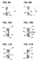
- FIGS. 9A and 9B are enlarged cross-sectional views of hole portions according to a modification of the second embodiment;
- FIG. 10A is an enlarged cross-sectional view of a hole portion according to another modification of the second embodiment, and FIG. 10B is a view of FIG. 10A when a second end portion of the male connector of FIG. 7A is inserted through the hole portion;
- FIGS. 11A and 11B are enlarged cross-sectional view of hole portions according to another modification of the second embodiment;
- FIG. 12 is a cross-sectional view of a connector terminal according to a modification of the present invention;
- FIG. 13 is a cross sectional view of a projection of a connector terminal according to a modification of the present invention; and
- FIG. 14 is a cross-sectional view of a connector housing according to a modification of the present invention.
- As shown in FIGS. 1A-1C, an
electronic apparatus 100 includes acircuit board 200, amale connector 300 surface-mounted to thecircuit board 200, and acasing 400 for housing thecircuit board 200. Themale connector 300 has a connector mounting structure according to a first embodiment of the present invention. Asealant 500 seals theelectronic apparatus 100 so that an inner space S of theelectronic apparatus 100 is waterproofed, i.e., protected from water damage. For example, therefore, theelectronic apparatus 100 may be suitable for an engine electronic control unit (ECU) installed in an engine room, which is located on the exterior of a vehicle. - The
circuit board 200 includes a printedboard 210 and electronic devices mounted to the printedboard 210. For example, the electronic devices are a microcomputer, a resistor, a capacitor, and the like, which are not shown in the drawings. Themale connector 300 is one example of the electronic devices. The printedboard 210 is provided with conductive patterns and via holes for connecting the conductive patterns. The printedboard 210 is made of a known material such as a thermoplastic resin, a thermoset resin, a ceramic, or a glass/resin composite material (e.g., glass-cloth). In the first embodiment, the printedboard 210 is a multilayered board that uses a FR-5-equivalent board made of a glass/epoxy-resin composite material and has a multi-layered conductive pattern. - The
male connector 300 includes aconnector housing 320 and a plurality offirst terminals 310a mounted in theconnector housing 320. Each first terminal 310a is made of an electrically conductive material such as a metal plated brass. Theconnector housing 320 is made of an electrically insulating material such as a synthetic resin. Themale connector 300 is mounted to thecircuit board 200 and acts as an input/output interface of thecircuit board 200. - The
connector housing 320 includes abody member 330 and a fixingmember 340. Thebody member 330 and the fixingmember 340 are separate pieces. Each of thefirst terminals 310a is mounted to thebody member 330. The fixingmember 340 has first, second, and third fixing portion 341-343. The first, second, and third fixing portions 341-343 are used to fix the fixingmember 340 to, an external female connector to be mated with themale connector 300, thecasing 400 via thesealant 500, and thebody member 330, respectively. At least thefirst fixing portion 341 is shaped like a tube to receive a connector housing of the female connector. - As shown in FIGS. 1A, 2A, and 2B, each of the
first terminals 310a has afirst end portion 311 a, asecond end portion 312a, and ajoint portion 313a. Thefirst end portion 311 a is exposed to a firstlongitudinal surface 331 of thebody member 330 and soldered to a conductive land formed on a mounting surface of the printedboard 210. Thesecond end portion 312a is also exposed to the firstlongitudinal surface 331 of thebody member 330 to be electrically connectable to the female connector. Therefore, thefirst end portion 311 a and thesecond end portion 312a extend to the same side with respect to thebody member 330. Thejoint portion 313a connects thefirst end portion 311 a and thesecond end portion 312a so that thefirst terminal 310a is approximately C-shaped. Thefirst end portion 311 a is positioned below thesecond end portion 312a in a thickness direction of thecircuit board 200 in a condition where thefirst terminal 310a is mounted to the circuit board 200 (i.e., thefirst end portion 311a is soldered to the conductive land formed on the mounting surface of the circuit board 200). - The
body member 330 is shaped like an approximately rectangular solid and has the firstlongitudinal surface 331. The firstlongitudinal surface 331 of thebody member 330 is approximately perpendicular to the mounting surface of thecircuit board 200. As described above, each of the first andsecond end portions longitudinal surface 331. Thus, thefirst terminals 310a are arranged in a longitudinal direction of thebody member 330. - As shown in FIG. 2C, the
body member 330 has a plurality ofslits 332 on the firstlongitudinal surface 331. Thejoint portion 313a of thefirst terminal 310a is placed and fixed in a corresponding one of theslits 332. Eachslit 332 has a depth enough to fully accommodate thejoint portion 313a so that thejoint portion 313a is not exposed to the firstlongitudinal surface 331. Therefore, short-circuit caused by a conductiveforeign matter 600 between adjacentjoint portions 313a can be reduced. - As shown in FIGS. 2A and 2B, an
engagement portion 333 is integrally provided on each of side surfaces, adjacent to the firstlongitudinal surface 331, and a top surface of thebody member 330. Thebody member 330 and the fixingmember 340 are fixed together by theengagement portion 333. - As described above, the fixing
member 340 has a tube portion at least at thefirst fixing portion 341, as shown in FIG. 3A. The connector housing of the female connector is received in the tube portion of the fixingmember 340 so that themale connector 300 can be mated with the female connector. The first, second, and third fixing portions 341-343 of the fixingmember 340 are arranged in that order from an open side of the tube portion where themale connector 300 is mated with the female connector. When thebody member 330 of themale connector 300 is mounted to thecircuit board 200 and fixed to the fixingmember 340, thecircuit board 200 and thebody member 330 are at least partially received in the tube portion of the fixingmember 340 so that thefirst end portion 311 a of thefirst terminal 310a is placed inside the tube portion. - The first, second, and third fixing portions 341-343 are described in detail below. First and
second projections member 340. Thefirst fixing portion 341 extends from the opening of the tube portion to an edge of thesecond projection 345. Therefore, thefirst fixing portion 341 includes thefirst projection 344 and a first recess between the first andsecond projections second projection portion 345. Thefirst projection 344 can be received in a receiver of the connector housing of the female connector. Thesecond fixing portion 342 includes thesecond projection 345 and a second recess. The first and second recesses are opposite to each other across thesecond projection 345. Return to FIG. 1 A, thesealant 500 is disposed in the second recess, and anopening edge 430 of a connector opening of thecasing 400 is attached to the second recess through thesealant 500. The rest of the fixingmember 340 is thethird fixing portion 343. Aslit 346 for receiving theengagement portion 333 of thebody member 330 is provided on an inner surface of thethird fixing portion 343 of the fixingmember 340. - As shown in FIG. 3C, a guiding
slit 349 for receiving both sides of thecircuit board 200 is provided on an inner surface of the fixing member 340 (specifically, the second and third fixingportions 342, 343). Thecircuit board 200 can be positioned with respect to the fixingmember 340 by inserting both sides of thecircuit board 200 into the guidingslit 349. The guiding slit 349 has a predetermined length and extends in a longitudinal direction of the fixingmember 340 from an opposite side to the open side of the tube portion. The guiding slit 349 has a uniform width equal to or slightly larger than a thickness of the printedboard 210. - As described above, the
connector housing 320 of themale connector 300 is assembled as one piece from the separate pieces, i.e., thebody member 330 and the fixingmember 340. Therefore, themale connector 300 can be easily and reliably mounted to thecircuit board 200 as follows. - First, the
body member 330 is mounted to thecircuit board 200 by reflow soldering. Specifically, thefirst end portion 311a exposed to the firstlongitudinal surface 331 of thebody member 330 is soldered to the conductive land formed on the printedboard 200. - Second, the
circuit board 200 is positioned with respect to the fixingmember 340 by using the guidingslit 349. - Finally, the
engagement portion 333 of thebody member 330 is received in theslit 346 of the fixingmember 340 so that thebody member 330 and the fixingmember 340 are fixed together. - Thus, the
male connector 300 is mounted to thecircuit board 200 by using the connector mounting structure according to the first embodiment. - Further, as shown FIGS. 1A, 3A, the fixing
member 340 includes first andsecond protection portions member 340 and made of the same material as the fixingmember 340. - The
first protection portion 347 projects from a bottom inner surface of the tube portion of the fixingmember 340. In the condition where thebody member 330 and the fixingmember 340 are fixed together, thefirst protection portion 347 is placed between the first andsecond end portions circuit board 200 and touches the firstlongitudinal surface 331 of thebody member 330. Thefirst protection portion 347 covers at least a first facing area between adjacentfirst end portions 311 a without touching the adjacentfirst end portions 311 a. Thus, it is unlikely oneforeign matter 600 touches both the adjacentfirst end portions 311 a at the same time. Thus, short-circuit caused by theforeign matter 600 between the adjacentfirst end portions 311 a can be reduced. - The
first protection portion 347 extends from a first point further away from the firstlongitudinal surface 331 of thebody member 330 than a second point to which thefirst end portion 311 a extends. When theforeign matter 600 falls and stays on thefirst protection portion 347, theforeign matter 600 may cause short circuit between adjacentsecond end portions 312a. Thefirst protection portion 347 has a slope portion so that a gap between thefirst protection portion 347 and the mounting surface of thecircuit board 200 decreases with distance from thebody member 330. When theforeign matter 600 falls on thefirst protection portion 347, theforeign matter 600 rolls or slides down thefirst protection portion 347 away from thebody member 330, as shown in FIG.1A. Thus, the short-circuit caused by theforeign matter 600 between adjacentsecond end portions 312a can be reduced. - The
second protection portion 348 projects from a top inner surface of the fixingmember 340. In the condition where thebody member 330 and the fixingmember 340 are fixed together, thesecond protection portion 348 touches an edge portion of the firstlongitudinal surface 331 of thebody member 330. Thesecond protection portion 348 prevents theforeign matter 600 from entering the inner space S of thecasing 400 via a clearance between thebody member 330 and the fixingmember 340. Thesecond protection portion 348 reduces or complicates the clearance, i.e., a passage to the inner space S. Preferably, thesecond protection portion 348 seals the clearance. In the first embodiment, thesecond protection portion 348 projects inwardly from the inner surface of thethird fixing portion 343 of the fixingmember 340, as shown in FIG. 3A. - The
casing 400 is made of synthetic resin or metal such as aluminum or iron. Thecasing 400 includes acase 410 shaped like a box with an opening and acover 420 shaped like a rectangular plate. Thecover 420 is attached to thecase 410 by a screw, for example. Thus, the opening of thecase 410 is covered with thecover 420 to produce the inner space S of thecasing 400. In the first embodiment, thecasing 400 is constructed from two pieces, i.e., thecase 410 and thecover 420. Alternatively, thecasing 400 may be a single piece or constructed from three or more pieces. Thecircuit board 200 is sandwiched between thecase 410 and thecover 420 through anelastic member 510 such as a rubber. Thus, thecircuit board 200 is fixed to thecasing 400. - The
casing 400 has the connector opening for receiving themale connector 300. Due to the connector opening, thesecond end portion 312a of the first terminal 310a of themale connector 300 is exposed outside thecasing 400 in a condition where thecircuit board 200 is housed in thecasing 400. Thus, thecircuit board 200 can be electrically connected to the female connector through themale connector 300. As described above, in the first embodiment, thesealant 500 is placed between the openingedge 430 of the connector opening of thecasing 400 and thesecond fixing portion 342 of the fixingmember 340. - The
sealant 500 is made of a material having elasticity and adhesion enough to seal thecasing 400. The inner space S of thecasing 400 is protected from the water damage in a condition where themale connector 300 is mated with the female connector. For example, thesealant 500 is moisture curing silicone adhesive having hardness (i.e., viscosity) of between 150 pascal-second (Pa·s) and 200 Pa·s before the adhesive cures. Alternatively, thesealant 500 may be a material disclosed inJP-2005-93602 - In the connector mounting structure according to the first embodiment, the
male connector 300 includes thefirst terminal 310a having the first andsecond end portions second end portions longitudinal surface 331 of thebody member 330. Theconnector housing 320 of themale connector 300 is assembled as one piece from the separate pieces, i.e., thebody member 330 and the fixingmember 340. In the condition where thebody member 330 is mounted to thecircuit board 200 by the reflow soldering, thebody member 330 and the fixingmember 340 are fixed together. In such an approach, thecircuit board 200 can be reduced in size in the direction along the mounting surface. - The fixing
member 340 has thefirst protection portion 347. In the condition where thebody member 330 and the fixingmember 340 are fixed together, thefirst protection portion 347 is placed between the first andsecond end portions circuit board 200 to cover at least the facing area between adjacentfirst end portions 311a. Thus, it is unlikely oneforeign matter 600 touches both the adjacentfirst end portions 311a at the same time. Therefore, distance between adjacentfirst terminals 310a can be reduced. In such an approach, thecircuit board 200 can be reduced in size in the direction along the mounting surface without increasing the possibility of the short-circuit caused by theforeign matter 600. - The fixing
member 340 further has thesecond protection portion 348. In the condition where thebody member 330 and the fixingmember 340 are fixed together, thesecond protection portion 348 touches the edge portion of the firstlongitudinal surface 331 to seal the clearance between thebody member 330 and the fixingmember 340. Thus, thesecond protection portion 348 prevents theforeign matter 600 from entering the inner space S of thecasing 400 via the clearance between thebody member 330 and the fixingmember 340. - In the first embodiment, the
first protection portion 347 extends from the first point further away from the firstlongitudinal surface 331 than the second point to which thefirst end portion 311a extends. In such an approach, the short-circuit between the adjacentfirst end portions 311a can be surely prevented. Alternatively, thefirst protection portion 347 may be provided as shown in FIGS. 4A and 4B, where thefirst protection portion 347 covers only the facing area between the adjacentfirst end portions 311a. - In the first embodiment, the
first protection portion 347 has the slope portion so that the gap between thefirst protection portion 347 and the mounting surface of thecircuit board 200 decreases with the distance from thebody member 330. When theforeign matter 600 falls on thefirst protection portion 347, theforeign matter 600 rolls or slides down thefirst protection portion 347 away from thebody member 330. Therefore, even if gap between thefirst protection portion 347 and thesecond end portion 312a is small, the short-circuit caused by theforeign matter 600 between the adjacentsecond end portions 312a can be reduced. Alternatively, as shown in FIG. 5, thefirst protection portion 347 may not have the slope portion. In this case, the gap between thefirst protection portion 347 and thesecond end portion 312a needs to be increased. - Further, the
first protection portion 347 touches the firstlongitudinal surface 331 of thebody member 330 to prevent theforeign matter 600 from entering the first facing area between the adjacentfirst end portions 311 a via a clearance between thefirst protection portion 347 and the firstlongitudinal surface 331. In such an approach, the short-circuit caused by theforeign matter 600 between the adjacentfirst end portions 311a can be surely reduced. In contrast, in the case of FIG. 5, thefirst protection portion 347 does not touch the firstlongitudinal surface 331. Therefore, the clearance between thefirst protection portion 347 and the firstlongitudinal surface 331 needs to be sealed with something. - In the first embodiment, the
first protection portion 347 is unitary with the fixingmember 340. Thus, structure of themale connector 300 can be simplified so that manufacturing steps can be reduced. Alternatively, as shown in FIG. 6, thefirst protection portion 347 may be separated from the fixingmember 340. In the case of FIG. 6, an electrically insulating material (e.g., protective gel) coating on thefirst end portion 311 a serves as thefirst protection portion 347. - When the
first protection portion 347 is made of the electrically insulating material, it is preferable that thefirst protection portion 347 should be placed as close to thefirst end portion 311 a as possible, as in the case of FIG. 5. In such an approach, gap between thefirst protection portion 347 and thesecond end portion 312a is increased so that the short-circuit caused by theforeign matter 600 between the adjacentsecond end portions 312a can be reduced. It is more preferable that thefirst protection portion 347 should touch thefirst end portion 311a, as in the case of FIG. 6. - The second embodiment of the present invention is described with reference to FIGS. 7A, 7B, and 8.
- As described above, in the first embodiment, the
joint portion 313a of thefirst terminal 310a is placed in theslit 332 and fixed inside thebody member 330. Theslit 332 has the depth enough to fully accommodate thejoint portion 313a so that thejoint portion 313a is not exposed to the firstlongitudinal surface 331, i.e., a whole portion of thejoint portion 313a is placed in theslit 332. Thus, the short-circuit caused by theforeign matter 600 between the adjacentjoint portions 313a is reduced by adjusting the depth of theslit 332. - In the second embodiment, the fixing
member 340 has athird protection portion 350 and does not have thesecond protection portion 348. Thethird protection portion 350 is provided in front of the firstlongitudinal surface 331 of thebody member 330 to cover at least thejoint portion 313a and a second facing area between the adjacentjoint portions 313a in the condition where thebody member 330 and the fixingmember 340 are fixed together. The short-circuit caused by theforeign matter 600 between the adjacentjoint portions 313a can be reduced by thethird protection portion 350. - When the
male connector 300 is mated with the female connector, a contact portion of thesecond end portion 312a is electrically connected to the female connector. At least the contact portion of thesecond end portion 312a is placed further forward than thethird protection portion 350 with respect to the firstlongitudinal surface 331 of thebody member 330. Thus, although thethird protection portion 350 is provided in front of the firstlongitudinal surface 331, thesecond end portion 312a can be electrically connected to the female connector. - In the first embodiment, although the
joint portion 313a is placed in theslit 332, a portion of thejoint portion 313a is exposed as shown in FIG. 2C. In contrast, in the second embodiment, thethird protection portion 350 covers both thejoint portion 313a and the second facing area between the adjacentjoint portions 313a. Thus, in the second embodiment, the short-circuit caused by theforeign matter 600 between the adjacentjoint portions 313a can be reduced compared to in the first embodiment. - As shown in FIGS. 7A, 7B, the
third protection portion 350 is unitary with the fixingmember 340 and made of the same material as the fixingmember 340. Thethird protection portion 350 is also unitary with thefirst protection portion 347. Thus, the structure of themale connector 300 can be simplified so that the manufacturing steps can be reduced. In the second embodiment, thethird protection portion 350 unitary with thefirst protection portion 347 is provided in front of the firstlongitudinal surface 331 to block the tube portion of the fixingmember 340 to pass through between thesecond end portions 312a of thefirst terminal 310a. Thus, thethird protection portion 350 seals the clearance between thebody member 330 and the fixingmember 340. In short, thethird protection portion 350 can serve as thesecond protection portion 348 and prevent theforeign matter 600 from entering the inner space S of thecasing 400 via the clearance. As with the first embodiment, thefirst protection portion 347 has the slope portion. - The
third protection portion 350 includes abase portion 351 andhole portions 352 defined byinner walls 353 of thebase portion 351. Thebase portion 351 is placed approximately parallel to the firstlongitudinal surface 331. Eachsecond end portion 312a is inserted through a corresponding one of thehole portions 352. It is preferable that thethird protection portion 350 should be placed as close to the firstlongitudinal surface 331 as possible to reduce the length of thesecond end portion 312a, i.e., to reduce the size of theelectronic apparatus 100. It is more preferable that thethird protection portion 350 should touch the firstlongitudinal surface 331. In the second embodiment, thethird protection portion 350 is placed as close to the firstlongitudinal surface 331 as possible with space in the condition where thebody member 330 and the fixingmember 340 are fixed together. - As shown in FIGS. 7A, 7B, each
hole portion 352 is a through hole that penetrates thebase portion 351. The diameter of thehole portion 352 on the side where themale connector 300 is mated with the female connector is slightly larger than the diameter of thesecond end portion 312a. Thehole portion 352 is tapered so that the diameter of thehole portion 352 is larger on thebody member 330 side than on the side where themale connector 300 is mated with the female connector. Thus, eachinner wall 353 of thehole portion 352 acts as a guiding member for guiding thesecond end portion 312a through thehole portion 352. Thefirst terminal 310a can be positioned with respect to thebody member 330 by inserting thesecond end portion 312a through thehole portion 352 of thethird protection portion 350. Due to the fact that thehole portion 352 is tapered, thesecond end portion 312a can be easily inserted though thehole portion 352 without hitting against thebase portion 351. Therefore, stress caused by the hit on junction between thefirst end portion 311a and thecircuit board 200 can be reduced so that connection reliability between thefirst end portion 311a and thecircuit board 200 can be ensured. - In the second embodiment, as shown in FIG. 8, the
second end portion 312a except the contact portion has aprojection 314a extending toward thebody member 330. Theprojection 314a is placed further forward than thethird protection portion 350 with respect to the firstlongitudinal surface 331 of thebody member 330. Therefore, the contact portion of thesecond end portion 312a can be electrically connected to the female connector. Even when stress in a direction opposite to the insertion direction of thesecond end portion 312a is applied to thesecond end portion 312a in the condition where thebody member 330 and the fixingmember 340 are fixed together, theprojection 314a of thesecond end portion 312a catches thethird protection portion 350 to ensure the electrical connection between thesecond end portion 312a and the female connector. Thus, themale connector 300 can be reliably mated with the female connector. - According to the second embodiment, the
third protection portion 350 is unitary with thefirst protection portion 347 and is provided in front of the firstlongitudinal surface 331 of thebody member 330. Thethird protection portion 350 reduces the short-circuit not only between the adjacentjoint portions 313a but also the adjacentfirst end portions 311a. Thethird protection portion 350 covers both thejoint portion 313a and the second facing area between the adjacentjoint portions 313a. In the second embodiment, therefore, the short-circuit between the adjacentjoint portions 313a can be surely reduced compared to in the first embodiment. - As described above, in the second embodiment, the diameter of the
hole portion 352 changes over the thickness of thebase portion 351 so that thehole portion 352 is fully tapered, i.e., does not have an uniform diameter portion. Alternatively, as shown in FIGS. 9A, 9B, thehole portion 352 may be partially tapered. In the case of FIG. 9A, thehole portion 352 is defined by a firstinner wall 353a and a secondinner wall 353b. The firstinner wall 353a is on the side of thebody member 330 and thehole portion 352 has a large diameter at the firstinner wall 353a than at the secondinner wall 353b. Thehole portion 352 is not tapered at the firstinner wall 353a and is tapered at the secondinner wall 353b. In short, thehole portion 352 has an uniform diameter at the secondinner wall 353b. The firstinner wall 353a acts in the same manner as theinner wall 353 shown in FIG. 8. In the case of FIG. 9B, thehole portion 352 is defined by the firstinner wall 353a and a thin-walled portion 353c that replaces the secondinner wall 353b. As shown in FIG. 9B, the thin-walled portion 353c projects toward the center of thehole portion 352 and is thinned to be deformable. Therefore, even when the thin-walled portion 353c touches thesecond end portion 312a by the difference in thermal expansion coefficient between thebody member 330 and the fixingmember 340, stress applied to thesecond end portion 312a by the thin-walled portion 353c can be reduced due to the deformation of the thin-walled portion 353c. Further, even when thesecond end portion 312a is slightly displaced with respect to thecorresponding hole portion 352 in the insertion step, thesecond end portion 312a can be inserted through thehole portion 352 due to the deformation of the thin-walled portion 353c. - As described above, in the second embodiment, the
hole portion 352 is a through hole. Alternatively, thehole portion 352 may be a blind hole and have a bottom before thesecond end portion 312a is inserted through thehole portion 352. For example, thesecond end portion 312a may penetrate the bottom of thehole portion 352 by using force caused when thebody member 330 and the fixingmember 340 are fixed together. Specifically, as shown in FIG. 10A, thethird protection portion 350 includes athin film member 354 having a first surface bonded on thebase portion 351 via anadhesive member 355 and a second surface facing the firstlongitudinal surface 331 of thebody member 330. Thethin film member 354 serves as the bottom of thehole portion 352 so that thehole portion 352 can be the blind hole before thesecond end portion 312a is inserted through thehole portion 352. As shown in FIG. 10B, thesecond end portion 312a penetrates thethin film member 354, when thebody member 330 and the fixingmember 340 are fixed together. Thus, thesecond end portion 312a can be inserted through thehole portion 352. Further, thesecond end portion 312a penetrates thethin film member 354 from the side of the second surface, where theadhesive member 355 is not applied, to prevent adhesion of theadhesive member 355 to thesecond end portion 312a. Thus, adhesion of the foreign matter 60 to thesecond end portion 312a can be prevented. Thethin film member 354 is made of an electrically insulating material. - In the case of FIGS. 10A, 10B, the
adhesive member 355 is applied to the entire first surface of thethin film member 354. Alternatively, as shown in FIG. 11A, theadhesive member 355 may be applied to the first surface of thethin film member 354 except the bottom of thehole portion 352 to surely prevent the adhesion of theadhesive member 355 to thesecond end portion 312a. In the case of FIGS. 10A, 10B, 11A, thethin film member 354 is bonded to thebase portion 351 on the side of thebody member 330. Alternatively, as shown in FIG. 11B, thethin film member 354 may be bonded to thebase portion 351 on the side of the female connector. - As described above, in the second embodiment, the
third protection portion 350 is unitary with the fixingmember 340 and made of the same material as the fixingmember 340. Further, thethird protection portion 350 is unitary with thefirst protection portion 347. Alternatively, thethird protection portion 350 may not be unitary with the fixingmember 340 and/or may not be unitary with thefirst protection portion 347. In this case, it is required that thethird protection portion 350 is placed in front of the firstlongitudinal surface 331 to cover at least thejoint portion 313a and the facing area between the adjacentjoint portions 313a. Further, it is required that at least the contact portion of thesecond end portion 312a is placed further forward than thethird protection portion 350 with respect to the firstlongitudinal surface 331 of thebody member 330. - The embodiments described above may be modified in various ways. For example, at least one of the
first terminals 310a may be placed with asecond terminal 310b. Thesecond terminal 310b has athird end portion 311b, afourth end portion 312b, and ajoint portion 313b, which are correspond to thefirst end portion 311a, thesecond end portion 312a, and thejoint portion 313a of thefirst terminal 310a, respectively. As shown in FIG. 12, while thefirst end portion 311a is exposed to and extends from the firstlongitudinal surface 331 of thebody member 330, thethird end portion 311b is exposed to and extends from a second longitudinal surface opposite to the firstlongitudinal surface 331. - As shown in FIG. 13, the
fourth end portion 312b may have aprojection 314b corresponding to theprojection 314a of thesecond end portion 312a. Theprojections base portion 351 of thethird protection portion 350 in the insertion step where the second andfourth end portions hole portion 352 in an insertion direction indicated by anarrow 10 of FIG. 13. When theprojections base portion 351, force is applied to thejoint portions arrow 20 of FIG. 13. In the case of thefirst terminal 310a, thebody member 330 is placed in the force direction indicated by thearrow 20 with respect to thejoint portion 313a. Therefore, even when theprojection 314a hits against thebase portion 351 in the insertion step, thefirst terminal 310a can remain fixed to thebody member 330. In contrast, in the case of thesecond terminal 310b, thebody member 330 is placed in the opposite direction to the force direction indicated by thearrow 20 with respect to thejoint portion 313b. Therefore, when theprojection 314b hits against thebase portion 351 in the insertion step, thesecond terminal 310b may be detached from thebody member 330. Therefore, it is preferable that when themale connector 300 has both thesecond end portion 312a and thefourth end portion 312b, thefourth end portion 312b does not have theprojection 314b. - In the embodiments described above, upper and lower portions of the fixing
member 340 with respect to thecircuit board 200 may have different length in thecasing 400, as shown in FIG. 1A. Alternatively, the upper and lower portions of the fixingmember 340 may have the same length in thecasing 400. - In the embodiments described above, the
circuit board 200 and thebody member 330 are at least partially received in the tube portion of the fixingmember 340 as shown in FIG. 1A. Alternatively, a whole portion of thebody member 330 may be outside the tube portion of the fixingmember 340. Alternatively, a whole portion of each of thecircuit board 200 and thebody member 330 may be placed outside the tube portion of the fixingmember 340, as shown in FIG. 14. - In the embodiments described above, the
male connector 300 is used in theelectronic apparatus 100, the inner space S of which is waterproofed by thesealant 500. In other words, themale connector 300 is used in a waterproof application. Alternatively, themale connector 300 can be used in a non-waterproof application. - Such changes and modifications are to be understood as being within the scope of the present invention as defined by the appended claims.
Claims (22)
- A connector mounting structure comprising:a circuit board (200); anda male connector (300) capable of being mated with an external female connector, the male connector (300) being surface-mounted to the circuit board (200) and including a connector housing (320) and a plurality of first male terminals (310a), whereinthe connector housing (320) includes a body member (330) and a fixing member (340) fixed to the body member (330), the body member (330) having a first surface (331), the fixing member (340) having a tube portion and a first protection portion (347), the tube portion receiving the female connector,each of the plurality of first male terminals (310a) is fixed in the body member (330) and has first and second end portions (311a, 312a) and a first joint portion (313a), the first end portion (311a) being exposed to the first surface (331) of the body member (330) and electrically connected to the circuit board (200), the second end portion (312a) being exposed to the first surface (331) of the body member (330) and placed above the first end portion (311a) in a thickness direction of the circuit board (200) to be electrically connectable to a terminal of the female connector, the first joint portion (313a) connecting the first and second end portions (311a, 312a) and being fixed in the body member (330), andthe first protection portion (347) is placed between the first and second end portions (311a, 312a) in the thickness direction of the circuit board (200) to cover a first facing area between each adjacent first end portion (311a).
- The connector mounting structure according to claim 1, wherein
the first protection portion (347) covers the first end portion (311a) in addition to the first facing area. - The connector mounting structure according to claim 2, wherein
the first protection portion (347) is made of an electrically insulating material and touches the first end portion (311a). - The connector mounting structure according to claim 2, wherein
the first protection portion (347) is spaced from the first end portion (311a). - The connector mounting structure according to any of claims 1-4, wherein
the first protection portion (347) has a slope portion, and
a gap between the slope portion and the circuit board (200) decreases with a distance from the body member (330). - The connector mounting structure according to any one of claims 1-5, wherein
the first protection portion (347) extends from a first position of the fixing member (340) toward the first surface (331) of the body member (330),
the first end portion (311a) extends from the first surface (331) of the body member (330) to a second position of the fixing member (340), and
the first position is further away from the first surface (331) of the body member (330) than the second position. - The connector mounting structure according to any one of claims 1-6, wherein
the first protection portion (347) touches the first surface (331) of the body member (330). - The connector mounting structure according to any one of claims 1-7, wherein
the first protection portion (347) is made of the same material as the fixing member (340) and unitary with the fixing member (340). - The connector mounting structure according to any one of claims 1-8, wherein
the fixing member (340) further has a second protection portion (348) touching an edge portion of the first surface (331) of the body member (330). - The connector mounting structure according to any one of claims 1-9, wherein
the body member (330) has a plurality of slit portions (332) on the first surface (331), each of the plurality of slit portions (332) having a depth,
the first joint portion (313a) is fixed in a corresponding one of the plurality of slit portions (332) and has a thickness in the depth direction, and
the depth is greater than the thickness so that a whole portion of the first joint portion (313a) is placed inside the corresponding one of the plurality of slit portions (332). - The connector mounting structure according to any one of claims 1-10, wherein
the fixing member (340) further has a third protection portion (350) that is placed in front of the first surface (331) of the body member (330) to cover both the first joint portion (313a) and a second facing area between each adjacent first joint portion (313a),
the second end portion (312a) has a contact portion electrically connectable to the female connector, and
at least the contact portion of the second end portion (312a) is placed further forward than the third protection portion (350) with respect to the first surface (331) of the body member (330). - The connector mounting structure according to claim 11, wherein
the third protection portion (350) is unitary with the first protection portion (347). - The connector mounting structure according to claim 11 or 12, wherein
the third protection portion (350) is made of the same material as the fixing member (340) and unitary with the fixing member (340). - The connector mounting structure according to any one of claims 11-13, wherein
the third protection portion (350) has a base portion (351) and a plurality of hole portions (352), the base portion (351) having a first surface facing the first surface (331) of the body member (330) and a second surface opposite to the first surface of the base portion (351), each of the plurality of hole portions (352) being defined by an inner wall (353, 353a, 353b) of the base portion (351), and
at least the contact portion of the second end portion (312a) is inserted through a corresponding one of the plurality of hole portions (352) to be placed further forward than the third protection portion (350) with respect to the first surface (331) of the body member (330). - The connector mounting structure according to claim 14, wherein
the each of the plurality of hole portions (352) has a diameter that decreases with the distance from the first surface of the base portion (351) so that the diameter is larger at the first surface side of the base portion (351) than the second surface side of the base portion (351), and
the inner wall (353, 353a, 353b) of the base portion (351) guides the second end portion (312a) through the each of the plurality of hole portions (352). - The connector mounting structure according to claim 14 or 15, wherein
the inner wall (353, 353a, 353b) of the base portion (351) has a deformable thin-walled portion (353c) projecting toward a center of the each of the plurality of hole portions (352). - The connector mounting structure according to any one of claims 14-16, wherein
the each of the plurality of hole portions (352) is a through hole penetrating through the base portion (351). - The connector mounting structure according to claim 14 or 15, wherein
the third protection portion (350) further has a thin film member (354) attached to one of the first and second surfaces of the base portion (351),
the each of the plurality of hole portions is a blind hole having a bottom provided by the thin film member (354), and
at least the contact portion of the second end portion (312a) penetrates the thin film member (354) to be placed further forward than the third protection portion (350) with respect to the first surface (331) of the body member (330). - The connector mounting structure according to claim 18, wherein
the fixing member (340) further has an adhesive member (355) applied to the first surface of the base portion (351) of the third protection portion (350), and
the thin film member (354) is attached to the first surface of the base portion (351) through the adhesive member (355). - The connector mounting structure according to claim 18 or 19, wherein
the fixing member (340) further has an adhesive member (355) applied to the one of the first and second surfaces except a portion corresponding to the bottom of the each of the plurality of hole portions (352), and
the thin film member (354) is attached to the one of the first and second surfaces through the adhesive member (355). - The connector mounting structure according to any one of claims 11-20, wherein
the second end portion (312a) except the contact portion has a projection portion (314a) extending outwardly so that the second end portion (312a) has an increased diameter at the projection portion (314a), and
the projection portion (314a) is placed further forward than the third protection portion (350) with respect to the first surface (331) of the body member (330). - The connector mounting structure according to claim 21, wherein
the male connector (300) further includes a plurality of second male terminals (310b), and
each of the plurality of second male terminals (310b) is fixed in the body member (330) and has third and fourth end portions (311b, 312b) and a second joint portion (313b), the third end portion (311b) being exposed to a second surface opposite to the first surface (331) of the body member (330) and electrically connected to the circuit board (200), the fourth end portion (312b) being exposed to the first surface (331) of the body member (330) to be electrically connectable to the terminal of the female connector, the second joint portion (313b) connecting the third and fourth end portions (311b, 312b) and being fixed in the body member (330).
Applications Claiming Priority (1)
| Application Number | Priority Date | Filing Date | Title |
|---|---|---|---|
| JP2006134411A JP4661684B2 (en) | 2006-05-12 | 2006-05-12 | Connector mounting structure |
Publications (3)
| Publication Number | Publication Date |
|---|---|
| EP1855361A2 true EP1855361A2 (en) | 2007-11-14 |
| EP1855361A3 EP1855361A3 (en) | 2008-09-03 |
| EP1855361B1 EP1855361B1 (en) | 2010-02-24 |
Family
ID=38434687
Family Applications (1)
| Application Number | Title | Priority Date | Filing Date |
|---|---|---|---|
| EP07008795A Not-in-force EP1855361B1 (en) | 2006-05-12 | 2007-04-30 | Connector mounting structure |
Country Status (4)
| Country | Link |
|---|---|
| US (1) | US7390199B2 (en) |
| EP (1) | EP1855361B1 (en) |
| JP (1) | JP4661684B2 (en) |
| DE (1) | DE602007004899D1 (en) |
Cited By (6)
| Publication number | Priority date | Publication date | Assignee | Title |
|---|---|---|---|---|
| WO2012149232A1 (en) * | 2011-04-29 | 2012-11-01 | Tyco Electronics Corporation | Header connector assembly |
| EP2618430A1 (en) * | 2012-01-12 | 2013-07-24 | BIOTRONIK SE & Co. KG | Electrical connecting element and combination comprising an electrical connecting element and a component |
| KR101428933B1 (en) * | 2013-07-05 | 2014-08-08 | 현대오트론 주식회사 | Electronic control apparatus for vehicle using radiation board and manufacturing method thereof |
| EP2930791A1 (en) * | 2014-04-11 | 2015-10-14 | Tyco Electronics Japan G.K. | Surface mount connector |
| CN109644569A (en) * | 2016-06-30 | 2019-04-16 | 罗伯特·博世有限公司 | Method in particular for the controller unit of motor vehicle and for being fixed on the connector pin of the straight line of controller unit in the circuit board component of the controller unit |
| US11387603B2 (en) | 2016-03-31 | 2022-07-12 | Molex, Llc | Panel mount connector with terminal module secured to connector housing |
Families Citing this family (17)
| Publication number | Priority date | Publication date | Assignee | Title |
|---|---|---|---|---|
| EP2226185B1 (en) * | 2007-11-29 | 2017-04-26 | Ngk Spark Plug Co., Ltd. | Metal-resin compound member |
| JP4591510B2 (en) * | 2008-01-07 | 2010-12-01 | 株式会社デンソー | Connector and electronic control unit |
| US8506332B2 (en) | 2008-02-26 | 2013-08-13 | Molex Incorporated | Impedance controlled electrical connector |
| JP2012231004A (en) * | 2011-04-26 | 2012-11-22 | Honda Elesys Co Ltd | Conduction terminal solder stress prevention structure |
| JP2014154344A (en) * | 2013-02-08 | 2014-08-25 | Hitachi Metals Ltd | Connector supporting structure, and electronic device with connector |
| US9276350B1 (en) * | 2014-08-05 | 2016-03-01 | Ting Shen Industrial Co., Ltd. | Waterproof electric plug with transformer |
| DE102014223644A1 (en) * | 2014-11-19 | 2016-05-19 | Zf Friedrichshafen Ag | Plug arrangement with at least one plug element |
| JP6354874B1 (en) * | 2017-01-31 | 2018-07-11 | 住友大阪セメント株式会社 | Light modulator |
| JP6574805B2 (en) * | 2017-03-27 | 2019-09-11 | 矢崎総業株式会社 | Waterproof parts |
| BE1025487B1 (en) * | 2017-08-21 | 2019-03-27 | Phoenix Contact Gmbh & Co. Kg | ELECTRICAL CONNECTOR FOR THE CONSTRUCTION OF A PCB PLUG CONNECTOR TO A PCB |
| CN112821129B (en) * | 2017-08-31 | 2022-03-11 | 中航光电科技股份有限公司 | Backplane Connector Assemblies and Seal Assemblies for Backplane Connectors |
| KR102030824B1 (en) * | 2017-11-01 | 2019-10-10 | 현대오트론 주식회사 | Electronic control device |
| JP2019125617A (en) * | 2018-01-12 | 2019-07-25 | トヨタ自動車株式会社 | Manufacturing method of electric component and electric component |
| DE102018126543A1 (en) * | 2018-10-24 | 2020-04-30 | Schmidhauser Ag | Electrical connector, electrical device and method of manufacturing an electrical device |
| JP7432990B2 (en) * | 2018-11-13 | 2024-02-19 | タイコエレクトロニクスジャパン合同会社 | electrical equipment |
| DE102022112190A1 (en) | 2022-05-16 | 2023-11-16 | Brose Fahrzeugteile SE & Co. Kommanditgesellschaft, Coburg | Connector with a circuit board |
| JP2024089897A (en) * | 2022-12-22 | 2024-07-04 | パナソニックオートモーティブシステムズ株式会社 | Housing and electronics |
Citations (4)
| Publication number | Priority date | Publication date | Assignee | Title |
|---|---|---|---|---|
| US4781600A (en) | 1986-06-25 | 1988-11-01 | Yazaki Corporation | Junction box and a process of assembling the same |
| DE19805708A1 (en) | 1998-02-12 | 1999-09-09 | Siemens Ag | Plug device especially for motor vehicle electronic equipment |
| EP1380473A1 (en) | 2002-07-09 | 2004-01-14 | Valeo Electronique et Systemes de Liaison | Connection box |
| JP2006055383A (en) | 2004-08-20 | 2006-03-02 | Taketoshi Goto | Pillow for comfortably sleeping face-down |
Family Cites Families (11)
| Publication number | Priority date | Publication date | Assignee | Title |
|---|---|---|---|---|
| US4583807A (en) * | 1983-12-13 | 1986-04-22 | Amp Incorporated | Surface mount connector |
| JPH051913Y2 (en) * | 1989-07-10 | 1993-01-19 | ||
| JPH0754925Y2 (en) * | 1990-07-21 | 1995-12-18 | 本多通信工業株式会社 | connector |
| JP2872023B2 (en) * | 1993-11-10 | 1999-03-17 | 矢崎総業株式会社 | Surface mount connector |
| JPH07220780A (en) * | 1993-12-29 | 1995-08-18 | Whitaker Corp:The | Surface mount type connector |
| JP3279443B2 (en) * | 1994-09-08 | 2002-04-30 | ミツミ電機株式会社 | Data recording / reproducing device |
| JP3755989B2 (en) | 1998-06-15 | 2006-03-15 | 本多通信工業株式会社 | PCB connector |
| DE10045728B4 (en) * | 1999-09-17 | 2015-08-20 | Denso Corporation | Housing for an electronic control unit and arrangement of such a housing and an electronic circuit unit |
| JP4029703B2 (en) * | 2002-09-19 | 2008-01-09 | オムロン株式会社 | Flexible board connector |
| JP2004206924A (en) | 2002-12-24 | 2004-07-22 | Auto Network Gijutsu Kenkyusho:Kk | Connector mounting structure and mounting method |
| JP2005135765A (en) | 2003-10-30 | 2005-05-26 | Aisin Seiki Co Ltd | Electronic component assembly and method for assembling the electronic component assembly |
-
2006
- 2006-05-12 JP JP2006134411A patent/JP4661684B2/en not_active Expired - Fee Related
-
2007
- 2007-04-24 US US11/790,110 patent/US7390199B2/en not_active Expired - Fee Related
- 2007-04-30 EP EP07008795A patent/EP1855361B1/en not_active Not-in-force
- 2007-04-30 DE DE602007004899T patent/DE602007004899D1/en active Active
Patent Citations (4)
| Publication number | Priority date | Publication date | Assignee | Title |
|---|---|---|---|---|
| US4781600A (en) | 1986-06-25 | 1988-11-01 | Yazaki Corporation | Junction box and a process of assembling the same |
| DE19805708A1 (en) | 1998-02-12 | 1999-09-09 | Siemens Ag | Plug device especially for motor vehicle electronic equipment |
| EP1380473A1 (en) | 2002-07-09 | 2004-01-14 | Valeo Electronique et Systemes de Liaison | Connection box |
| JP2006055383A (en) | 2004-08-20 | 2006-03-02 | Taketoshi Goto | Pillow for comfortably sleeping face-down |
Cited By (13)
| Publication number | Priority date | Publication date | Assignee | Title |
|---|---|---|---|---|
| US8523581B2 (en) | 2011-04-29 | 2013-09-03 | Tyco Electronics Corporation | Header connector assembly |
| CN103493309A (en) * | 2011-04-29 | 2014-01-01 | 泰科电子公司 | Joint connector assembly |
| WO2012149232A1 (en) * | 2011-04-29 | 2012-11-01 | Tyco Electronics Corporation | Header connector assembly |
| EP2618430A1 (en) * | 2012-01-12 | 2013-07-24 | BIOTRONIK SE & Co. KG | Electrical connecting element and combination comprising an electrical connecting element and a component |
| US8920198B2 (en) | 2012-01-12 | 2014-12-30 | Biotronik Se & Co. Kg | Electrical connecting element and combination comprising an electrical connecting element and component |
| US9185831B2 (en) | 2013-07-05 | 2015-11-10 | Hyundai Autron Co., Ltd. | Electronic control apparatus for vehicle using radiation board and manufacturing method thereof |
| KR101428933B1 (en) * | 2013-07-05 | 2014-08-08 | 현대오트론 주식회사 | Electronic control apparatus for vehicle using radiation board and manufacturing method thereof |
| EP2930791A1 (en) * | 2014-04-11 | 2015-10-14 | Tyco Electronics Japan G.K. | Surface mount connector |
| CN104979686A (en) * | 2014-04-11 | 2015-10-14 | 泰科电子日本合同会社 | Surface mount connector |
| US9502809B2 (en) | 2014-04-11 | 2016-11-22 | Tyco Electronics Japan G.K. | Surface mount connector |
| CN104979686B (en) * | 2014-04-11 | 2019-06-11 | 泰科电子日本合同会社 | Surface Mount Connector |
| US11387603B2 (en) | 2016-03-31 | 2022-07-12 | Molex, Llc | Panel mount connector with terminal module secured to connector housing |
| CN109644569A (en) * | 2016-06-30 | 2019-04-16 | 罗伯特·博世有限公司 | Method in particular for the controller unit of motor vehicle and for being fixed on the connector pin of the straight line of controller unit in the circuit board component of the controller unit |
Also Published As
| Publication number | Publication date |
|---|---|
| EP1855361A3 (en) | 2008-09-03 |
| EP1855361B1 (en) | 2010-02-24 |
| JP4661684B2 (en) | 2011-03-30 |
| JP2007305494A (en) | 2007-11-22 |
| US7390199B2 (en) | 2008-06-24 |
| US20070264851A1 (en) | 2007-11-15 |
| DE602007004899D1 (en) | 2010-04-08 |
Similar Documents
| Publication | Publication Date | Title |
|---|---|---|
| US7390199B2 (en) | Connector mounting structure | |
| US7419385B2 (en) | Connector mounting structure and electronic apparatus having the same | |
| JP3673422B2 (en) | Branch connection box | |
| US6094349A (en) | Electrical device having a printed-circuit board and method for assembling the device | |
| EP2061292B1 (en) | Electronic control apparatus | |
| EP2034811B1 (en) | Electronic device including printed circuit board, connector and casing | |
| CN101630800B (en) | Through board inverted connector | |
| US9893459B2 (en) | Electrical connector having a tongue portion extending beyond a metallic shell | |
| EP2034809B1 (en) | Electronic device including printed circuit board and electronic element mounted on the printed circuit board | |
| JPH0629052A (en) | Connector | |
| US20070224890A1 (en) | Contact for a battery connector | |
| US20140045386A1 (en) | Connector and Manufacturing Method Thereof | |
| US20140342599A1 (en) | Electrical connector device | |
| KR19990067234A (en) | Electrical connector with frame | |
| JP4236940B2 (en) | Electronic control device case and electronic control device using this case | |
| JPWO2023135733A5 (en) | ||
| US20030157844A1 (en) | Electronic device having integrated connector | |
| JP4718891B2 (en) | Electrical junction box | |
| JP2007109993A (en) | Circuit board built-in housing | |
| JP2008176936A (en) | Connector device | |
| JP4700716B2 (en) | Connector that fits into the catcher of a vehicle antenna | |
| EP1471605A3 (en) | Electronic circuit unit having mounting structure with high soldering reliability | |
| JP4374297B2 (en) | Electrical junction box and manufacturing method thereof | |
| KR101899795B1 (en) | Electronic device having a housing made of profile material | |
| CN100397717C (en) | Connectors for printed circuit boards |
Legal Events
| Date | Code | Title | Description |
|---|---|---|---|
| PUAI | Public reference made under article 153(3) epc to a published international application that has entered the european phase |
Free format text: ORIGINAL CODE: 0009012 |
|
| AK | Designated contracting states |
Kind code of ref document: A2 Designated state(s): AT BE BG CH CY CZ DE DK EE ES FI FR GB GR HU IE IS IT LI LT LU LV MC MT NL PL PT RO SE SI SK TR |
|
| AX | Request for extension of the european patent |
Extension state: AL BA HR MK YU |
|
| PUAL | Search report despatched |
Free format text: ORIGINAL CODE: 0009013 |
|
| AK | Designated contracting states |
Kind code of ref document: A3 Designated state(s): AT BE BG CH CY CZ DE DK EE ES FI FR GB GR HU IE IS IT LI LT LU LV MC MT NL PL PT RO SE SI SK TR |
|
| AX | Request for extension of the european patent |
Extension state: AL BA HR MK RS |
|
| RIC1 | Information provided on ipc code assigned before grant |
Ipc: H01R 13/74 20060101AFI20070831BHEP Ipc: H01R 13/506 20060101ALI20080731BHEP Ipc: H01R 13/52 20060101ALI20080731BHEP |
|
| 17P | Request for examination filed |
Effective date: 20080910 |
|
| 17Q | First examination report despatched |
Effective date: 20081020 |
|
| AKX | Designation fees paid |
Designated state(s): DE FR IT |
|
| GRAP | Despatch of communication of intention to grant a patent |
Free format text: ORIGINAL CODE: EPIDOSNIGR1 |
|
| GRAS | Grant fee paid |
Free format text: ORIGINAL CODE: EPIDOSNIGR3 |
|
| GRAA | (expected) grant |
Free format text: ORIGINAL CODE: 0009210 |
|
| AK | Designated contracting states |
Kind code of ref document: B1 Designated state(s): DE FR IT |
|
| REF | Corresponds to: |
Ref document number: 602007004899 Country of ref document: DE Date of ref document: 20100408 Kind code of ref document: P |
|
| PLBE | No opposition filed within time limit |
Free format text: ORIGINAL CODE: 0009261 |
|
| STAA | Information on the status of an ep patent application or granted ep patent |
Free format text: STATUS: NO OPPOSITION FILED WITHIN TIME LIMIT |
|
| 26N | No opposition filed |
Effective date: 20101125 |
|
| PG25 | Lapsed in a contracting state [announced via postgrant information from national office to epo] |
Ref country code: IT Free format text: LAPSE BECAUSE OF NON-PAYMENT OF DUE FEES Effective date: 20100430 |
|
| REG | Reference to a national code |
Ref country code: DE Ref legal event code: R084 Ref document number: 602007004899 Country of ref document: DE Effective date: 20110705 Ref country code: DE Ref legal event code: R084 Ref document number: 602007004899 Country of ref document: DE Effective date: 20110610 |
|
| PGFP | Annual fee paid to national office [announced via postgrant information from national office to epo] |
Ref country code: FR Payment date: 20130625 Year of fee payment: 7 |
|
| PGFP | Annual fee paid to national office [announced via postgrant information from national office to epo] |
Ref country code: IT Payment date: 20130423 Year of fee payment: 7 |
|
| REG | Reference to a national code |
Ref country code: FR Ref legal event code: ST Effective date: 20141231 |
|
| PG25 | Lapsed in a contracting state [announced via postgrant information from national office to epo] |
Ref country code: FR Free format text: LAPSE BECAUSE OF NON-PAYMENT OF DUE FEES Effective date: 20140430 |
|
| PG25 | Lapsed in a contracting state [announced via postgrant information from national office to epo] |
Ref country code: IT Free format text: LAPSE BECAUSE OF NON-PAYMENT OF DUE FEES Effective date: 20140430 |
|
| PGFP | Annual fee paid to national office [announced via postgrant information from national office to epo] |
Ref country code: DE Payment date: 20220420 Year of fee payment: 16 |
|
| REG | Reference to a national code |
Ref country code: DE Ref legal event code: R119 Ref document number: 602007004899 Country of ref document: DE |
|
| PG25 | Lapsed in a contracting state [announced via postgrant information from national office to epo] |
Ref country code: DE Free format text: LAPSE BECAUSE OF NON-PAYMENT OF DUE FEES Effective date: 20231103 |