EP2034809B1 - Electronic device including printed circuit board and electronic element mounted on the printed circuit board - Google Patents
Electronic device including printed circuit board and electronic element mounted on the printed circuit board Download PDFInfo
- Publication number
- EP2034809B1 EP2034809B1 EP08013851.4A EP08013851A EP2034809B1 EP 2034809 B1 EP2034809 B1 EP 2034809B1 EP 08013851 A EP08013851 A EP 08013851A EP 2034809 B1 EP2034809 B1 EP 2034809B1
- Authority
- EP
- European Patent Office
- Prior art keywords
- circuit board
- printed circuit
- section
- terminals
- land
- Prior art date
- Legal status (The legal status is an assumption and is not a legal conclusion. Google has not performed a legal analysis and makes no representation as to the accuracy of the status listed.)
- Expired - Fee Related
Links
- 238000003780 insertion Methods 0.000 claims description 80
- 230000037431 insertion Effects 0.000 claims description 80
- 229910000679 solder Inorganic materials 0.000 claims description 61
- 238000004080 punching Methods 0.000 claims description 7
- 230000007423 decrease Effects 0.000 claims description 3
- 230000008878 coupling Effects 0.000 description 18
- 238000010168 coupling process Methods 0.000 description 18
- 238000005859 coupling reaction Methods 0.000 description 18
- 238000000034 method Methods 0.000 description 14
- 230000008569 process Effects 0.000 description 14
- 230000004048 modification Effects 0.000 description 6
- 238000012986 modification Methods 0.000 description 6
- 238000007789 sealing Methods 0.000 description 6
- 239000007789 gas Substances 0.000 description 4
- 239000011800 void material Substances 0.000 description 4
- 230000000052 comparative effect Effects 0.000 description 3
- 238000004519 manufacturing process Methods 0.000 description 3
- 229910052751 metal Inorganic materials 0.000 description 3
- 239000002184 metal Substances 0.000 description 3
- XEEYBQQBJWHFJM-UHFFFAOYSA-N Iron Chemical compound [Fe] XEEYBQQBJWHFJM-UHFFFAOYSA-N 0.000 description 2
- 239000011324 bead Substances 0.000 description 2
- 238000005452 bending Methods 0.000 description 2
- 230000004907 flux Effects 0.000 description 2
- 239000011521 glass Substances 0.000 description 2
- 239000000463 material Substances 0.000 description 2
- 230000003014 reinforcing effect Effects 0.000 description 2
- 229920005989 resin Polymers 0.000 description 2
- 239000011347 resin Substances 0.000 description 2
- 239000002904 solvent Substances 0.000 description 2
- 229910052782 aluminium Inorganic materials 0.000 description 1
- XAGFODPZIPBFFR-UHFFFAOYSA-N aluminium Chemical compound [Al] XAGFODPZIPBFFR-UHFFFAOYSA-N 0.000 description 1
- 239000003990 capacitor Substances 0.000 description 1
- 239000000919 ceramic Substances 0.000 description 1
- 239000004020 conductor Substances 0.000 description 1
- 238000001723 curing Methods 0.000 description 1
- 230000001419 dependent effect Effects 0.000 description 1
- 238000006073 displacement reaction Methods 0.000 description 1
- 230000000694 effects Effects 0.000 description 1
- 230000005611 electricity Effects 0.000 description 1
- 239000004744 fabric Substances 0.000 description 1
- -1 for example Inorganic materials 0.000 description 1
- 238000010438 heat treatment Methods 0.000 description 1
- 239000012774 insulation material Substances 0.000 description 1
- 229910052742 iron Inorganic materials 0.000 description 1
- 230000001678 irradiating effect Effects 0.000 description 1
- 238000013008 moisture curing Methods 0.000 description 1
- 238000000465 moulding Methods 0.000 description 1
- 238000003825 pressing Methods 0.000 description 1
- 238000007650 screen-printing Methods 0.000 description 1
- 239000013464 silicone adhesive Substances 0.000 description 1
- 238000005476 soldering Methods 0.000 description 1
- 125000006850 spacer group Chemical group 0.000 description 1
- 229920003002 synthetic resin Polymers 0.000 description 1
- 239000000057 synthetic resin Substances 0.000 description 1
- 229920005992 thermoplastic resin Polymers 0.000 description 1
- 229920001187 thermosetting polymer Polymers 0.000 description 1
Images


Classifications
-
- H—ELECTRICITY
- H05—ELECTRIC TECHNIQUES NOT OTHERWISE PROVIDED FOR
- H05K—PRINTED CIRCUITS; CASINGS OR CONSTRUCTIONAL DETAILS OF ELECTRIC APPARATUS; MANUFACTURE OF ASSEMBLAGES OF ELECTRICAL COMPONENTS
- H05K3/00—Apparatus or processes for manufacturing printed circuits
- H05K3/30—Assembling printed circuits with electric components, e.g. with resistor
- H05K3/32—Assembling printed circuits with electric components, e.g. with resistor electrically connecting electric components or wires to printed circuits
- H05K3/34—Assembling printed circuits with electric components, e.g. with resistor electrically connecting electric components or wires to printed circuits by soldering
- H05K3/3447—Lead-in-hole components
-
- H—ELECTRICITY
- H01—ELECTRIC ELEMENTS
- H01R—ELECTRICALLY-CONDUCTIVE CONNECTIONS; STRUCTURAL ASSOCIATIONS OF A PLURALITY OF MUTUALLY-INSULATED ELECTRICAL CONNECTING ELEMENTS; COUPLING DEVICES; CURRENT COLLECTORS
- H01R43/00—Apparatus or processes specially adapted for manufacturing, assembling, maintaining, or repairing of line connectors or current collectors or for joining electric conductors
- H01R43/02—Apparatus or processes specially adapted for manufacturing, assembling, maintaining, or repairing of line connectors or current collectors or for joining electric conductors for soldered or welded connections
- H01R43/0256—Apparatus or processes specially adapted for manufacturing, assembling, maintaining, or repairing of line connectors or current collectors or for joining electric conductors for soldered or welded connections for soldering or welding connectors to a printed circuit board
-
- H—ELECTRICITY
- H05—ELECTRIC TECHNIQUES NOT OTHERWISE PROVIDED FOR
- H05K—PRINTED CIRCUITS; CASINGS OR CONSTRUCTIONAL DETAILS OF ELECTRIC APPARATUS; MANUFACTURE OF ASSEMBLAGES OF ELECTRICAL COMPONENTS
- H05K1/00—Printed circuits
- H05K1/02—Details
- H05K1/11—Printed elements for providing electric connections to or between printed circuits
- H05K1/115—Via connections; Lands around holes or via connections
- H05K1/116—Lands, clearance holes or other lay-out details concerning the surrounding of a via
-
- H—ELECTRICITY
- H01—ELECTRIC ELEMENTS
- H01R—ELECTRICALLY-CONDUCTIVE CONNECTIONS; STRUCTURAL ASSOCIATIONS OF A PLURALITY OF MUTUALLY-INSULATED ELECTRICAL CONNECTING ELEMENTS; COUPLING DEVICES; CURRENT COLLECTORS
- H01R12/00—Structural associations of a plurality of mutually-insulated electrical connecting elements, specially adapted for printed circuits, e.g. printed circuit boards [PCB], flat or ribbon cables, or like generally planar structures, e.g. terminal strips, terminal blocks; Coupling devices specially adapted for printed circuits, flat or ribbon cables, or like generally planar structures; Terminals specially adapted for contact with, or insertion into, printed circuits, flat or ribbon cables, or like generally planar structures
- H01R12/50—Fixed connections
- H01R12/51—Fixed connections for rigid printed circuits or like structures
- H01R12/55—Fixed connections for rigid printed circuits or like structures characterised by the terminals
- H01R12/57—Fixed connections for rigid printed circuits or like structures characterised by the terminals surface mounting terminals
-
- H—ELECTRICITY
- H01—ELECTRIC ELEMENTS
- H01R—ELECTRICALLY-CONDUCTIVE CONNECTIONS; STRUCTURAL ASSOCIATIONS OF A PLURALITY OF MUTUALLY-INSULATED ELECTRICAL CONNECTING ELEMENTS; COUPLING DEVICES; CURRENT COLLECTORS
- H01R12/00—Structural associations of a plurality of mutually-insulated electrical connecting elements, specially adapted for printed circuits, e.g. printed circuit boards [PCB], flat or ribbon cables, or like generally planar structures, e.g. terminal strips, terminal blocks; Coupling devices specially adapted for printed circuits, flat or ribbon cables, or like generally planar structures; Terminals specially adapted for contact with, or insertion into, printed circuits, flat or ribbon cables, or like generally planar structures
- H01R12/50—Fixed connections
- H01R12/51—Fixed connections for rigid printed circuits or like structures
- H01R12/55—Fixed connections for rigid printed circuits or like structures characterised by the terminals
- H01R12/58—Fixed connections for rigid printed circuits or like structures characterised by the terminals terminals for insertion into holes
-
- H—ELECTRICITY
- H01—ELECTRIC ELEMENTS
- H01R—ELECTRICALLY-CONDUCTIVE CONNECTIONS; STRUCTURAL ASSOCIATIONS OF A PLURALITY OF MUTUALLY-INSULATED ELECTRICAL CONNECTING ELEMENTS; COUPLING DEVICES; CURRENT COLLECTORS
- H01R12/00—Structural associations of a plurality of mutually-insulated electrical connecting elements, specially adapted for printed circuits, e.g. printed circuit boards [PCB], flat or ribbon cables, or like generally planar structures, e.g. terminal strips, terminal blocks; Coupling devices specially adapted for printed circuits, flat or ribbon cables, or like generally planar structures; Terminals specially adapted for contact with, or insertion into, printed circuits, flat or ribbon cables, or like generally planar structures
- H01R12/70—Coupling devices
- H01R12/71—Coupling devices for rigid printing circuits or like structures
- H01R12/72—Coupling devices for rigid printing circuits or like structures coupling with the edge of the rigid printed circuits or like structures
- H01R12/722—Coupling devices for rigid printing circuits or like structures coupling with the edge of the rigid printed circuits or like structures coupling devices mounted on the edge of the printed circuits
- H01R12/724—Coupling devices for rigid printing circuits or like structures coupling with the edge of the rigid printed circuits or like structures coupling devices mounted on the edge of the printed circuits containing contact members forming a right angle
-
- H—ELECTRICITY
- H05—ELECTRIC TECHNIQUES NOT OTHERWISE PROVIDED FOR
- H05K—PRINTED CIRCUITS; CASINGS OR CONSTRUCTIONAL DETAILS OF ELECTRIC APPARATUS; MANUFACTURE OF ASSEMBLAGES OF ELECTRICAL COMPONENTS
- H05K2201/00—Indexing scheme relating to printed circuits covered by H05K1/00
- H05K2201/09—Shape and layout
- H05K2201/09209—Shape and layout details of conductors
- H05K2201/09372—Pads and lands
- H05K2201/09381—Shape of non-curved single flat metallic pad, land or exposed part thereof; Shape of electrode of leadless component
-
- H—ELECTRICITY
- H05—ELECTRIC TECHNIQUES NOT OTHERWISE PROVIDED FOR
- H05K—PRINTED CIRCUITS; CASINGS OR CONSTRUCTIONAL DETAILS OF ELECTRIC APPARATUS; MANUFACTURE OF ASSEMBLAGES OF ELECTRICAL COMPONENTS
- H05K2201/00—Indexing scheme relating to printed circuits covered by H05K1/00
- H05K2201/10—Details of components or other objects attached to or integrated in a printed circuit board
- H05K2201/10007—Types of components
- H05K2201/10189—Non-printed connector
-
- H—ELECTRICITY
- H05—ELECTRIC TECHNIQUES NOT OTHERWISE PROVIDED FOR
- H05K—PRINTED CIRCUITS; CASINGS OR CONSTRUCTIONAL DETAILS OF ELECTRIC APPARATUS; MANUFACTURE OF ASSEMBLAGES OF ELECTRICAL COMPONENTS
- H05K2201/00—Indexing scheme relating to printed circuits covered by H05K1/00
- H05K2201/10—Details of components or other objects attached to or integrated in a printed circuit board
- H05K2201/10613—Details of electrical connections of non-printed components, e.g. special leads
- H05K2201/10742—Details of leads
- H05K2201/1075—Shape details
- H05K2201/10787—Leads having protrusions, e.g. for retention or insert stop
-
- H—ELECTRICITY
- H05—ELECTRIC TECHNIQUES NOT OTHERWISE PROVIDED FOR
- H05K—PRINTED CIRCUITS; CASINGS OR CONSTRUCTIONAL DETAILS OF ELECTRIC APPARATUS; MANUFACTURE OF ASSEMBLAGES OF ELECTRICAL COMPONENTS
- H05K2201/00—Indexing scheme relating to printed circuits covered by H05K1/00
- H05K2201/10—Details of components or other objects attached to or integrated in a printed circuit board
- H05K2201/10613—Details of electrical connections of non-printed components, e.g. special leads
- H05K2201/10742—Details of leads
- H05K2201/1075—Shape details
- H05K2201/1084—Notched leads
-
- H—ELECTRICITY
- H05—ELECTRIC TECHNIQUES NOT OTHERWISE PROVIDED FOR
- H05K—PRINTED CIRCUITS; CASINGS OR CONSTRUCTIONAL DETAILS OF ELECTRIC APPARATUS; MANUFACTURE OF ASSEMBLAGES OF ELECTRICAL COMPONENTS
- H05K2201/00—Indexing scheme relating to printed circuits covered by H05K1/00
- H05K2201/10—Details of components or other objects attached to or integrated in a printed circuit board
- H05K2201/10613—Details of electrical connections of non-printed components, e.g. special leads
- H05K2201/10742—Details of leads
- H05K2201/1075—Shape details
- H05K2201/10848—Thinned leads
-
- H—ELECTRICITY
- H05—ELECTRIC TECHNIQUES NOT OTHERWISE PROVIDED FOR
- H05K—PRINTED CIRCUITS; CASINGS OR CONSTRUCTIONAL DETAILS OF ELECTRIC APPARATUS; MANUFACTURE OF ASSEMBLAGES OF ELECTRICAL COMPONENTS
- H05K2201/00—Indexing scheme relating to printed circuits covered by H05K1/00
- H05K2201/10—Details of components or other objects attached to or integrated in a printed circuit board
- H05K2201/10613—Details of electrical connections of non-printed components, e.g. special leads
- H05K2201/10742—Details of leads
- H05K2201/1075—Shape details
- H05K2201/10856—Divided leads, e.g. by slot in length direction of lead, or by branching of the lead
-
- H—ELECTRICITY
- H05—ELECTRIC TECHNIQUES NOT OTHERWISE PROVIDED FOR
- H05K—PRINTED CIRCUITS; CASINGS OR CONSTRUCTIONAL DETAILS OF ELECTRIC APPARATUS; MANUFACTURE OF ASSEMBLAGES OF ELECTRICAL COMPONENTS
- H05K2201/00—Indexing scheme relating to printed circuits covered by H05K1/00
- H05K2201/10—Details of components or other objects attached to or integrated in a printed circuit board
- H05K2201/10613—Details of electrical connections of non-printed components, e.g. special leads
- H05K2201/10742—Details of leads
- H05K2201/1075—Shape details
- H05K2201/10871—Leads having an integral insert stop
-
- H—ELECTRICITY
- H05—ELECTRIC TECHNIQUES NOT OTHERWISE PROVIDED FOR
- H05K—PRINTED CIRCUITS; CASINGS OR CONSTRUCTIONAL DETAILS OF ELECTRIC APPARATUS; MANUFACTURE OF ASSEMBLAGES OF ELECTRICAL COMPONENTS
- H05K2203/00—Indexing scheme relating to apparatus or processes for manufacturing printed circuits covered by H05K3/00
- H05K2203/11—Treatments characterised by their effect, e.g. heating, cooling, roughening
- H05K2203/1178—Means for venting or for letting gases escape
Description
- The present invention relates to an electronic device that includes a printed circuit board and an electronic element mounted on the printed circuit board.
- According to the prior art, an electronic device that includes a printed circuit board and an electronic element mounted on the printed circuit board has an insertion mounting structure and a surface mounting structure.
- For example, in an electronic device disclosed in
JP-A-11-317265 - When the insertion section is inserted into the through hole in which a solder paste is applied, air may be caught in the solder paste. In addition, a flux and a solvent component in the solder paste are gasified in the solder paste at a reflow process. The bubbles of air and gas move in the melted solder paste (i.e., in the through hole) toward an upper surface of the printed circuit board on which the electronic element is disposed.
- When the electronic element has the branch terminals, the surface sections of the branch terminals are located on the upper-surface side of the printed circuit board, which is the same side as the bubbles move to. The surface sections are located over at least portions of the through holes and the surface lands. In addition, in a thickness direction of the printed circuit board, lower surfaces of the surface sections are same height as upper surfaces of the surface lands or the lower surfaces of the surface sections are slightly away from the upper surfaces of the surface lands. Thus, even if the bubbles move upward and contact the surface sections, and then move in a direction perpendicular to the through holes (i.e., horizontal direction), sidewalls of the through holes are located in the moving direction. Thereby, the surface sections of the branch terminals restrict the movement of the bubbles. If a part of the bubbles remains in the solder paste, a void may be generated when the solder pasted is cooled and solidified. As a result, the branch terminals are difficult to be coupled with the printed circuit board with a high degree of certainty.
- Document
GB 2 019 093 A - In view of the foregoing problems, it is an object of the present invention to provide an electronic device that includes a printed circuit board and an electronic element coupled with the printed circuit board with a high degree of certainty.
- The object is solved by the features of the independent claims. The dependent claims are directed to preferred embodiments of the invention.
- In the present electronic device, bubbles of air and gas can be effectively released to an outside of the solder through the exhaust hole at a reflow process. Thus, the number of void can be reduced, and a connectivity of the electronic element with the printed circuit board can be improved.
- Additional objects and advantages of the present invention will be more readily apparent from the following detailed description of exemplary embodiments when taken together with the accompanying drawings. In the drawings:
-
FIG. 1 is an exploded view illustrating an electronic control device according to a first embodiment; -
FIG. 2 is an enlarged cross-sectional view illustrating a coupling portion of a connector with a printed circuit board; -
FIG. 3 is a plan view illustrating the connector viewed from a side where the printed circuit board is coupled; -
FIG. 4 is a plan view illustrating the connector viewed from a side where an external connector is coupled; -
FIG. 5 is a cross-sectional view illustrating the coupling portion taken along line V-V inFIG. 2 ; -
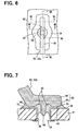
FIG. 6 is a plan view illustrating a coupling portion of a terminal and the printed circuit board; -
FIG. 7 is a cross-sectional view illustrating the coupling portion taken along line VII-VII inFIG. 6 ; -
FIG. 8 is a cross-sectional view illustrating the coupling portion taken along line VIII-VIII inFIG. 6 ; -
FIG. 9 is a cross-sectional view illustrating the coupling portion taken along line IX-IX inFIG. 6 ; -
FIG. 10 is a cross-sectional view illustrating a process at which an insertion section of a terminal is inserted into a through hole; -
FIG. 11 is a cross-sectional view illustrating movements of bubbles at a reflow process; -
FIG. 12 is a cross-sectional view illustrating a movement of a bubble at the reflow process; -
FIG. 13 is a cross-sectional view illustrating movements of bubbles in a coupling portion of a terminal with a printed circuit board according to a comparative example; -
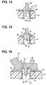
FIG. 14 is a cross-sectional view illustrating a movement of a bubble in the coupling portion of the terminal with the printed circuit board according to the comparative example; -
FIG. 15 is a cross-sectional view illustrating a movement of a bubble in a coupling portion of a terminal with a printed circuit board according to a first modification of the first embodiment; -
FIG. 16 is a cross-sectional view illustrating a coupling portion of a terminal with a printed circuit board according to a second modification of the first embodiment; -
FIG. 17 is a cross-sectional view illustrating a coupling portion of a terminal with a printed circuit board according to a third modification of the first embodiment; -
FIG. 18 is a cross-sectional view illustrating a movement of a bubble in a coupling portion of a terminal with a printed circuit board according to a fourth modification of the first embodiment; -
FIG. 19 is a cross-sectional view illustrating a coupling portion of a terminal with a printed circuit board according to a second embodiment; and -
FIG. 20 is a plan view illustrating a coupling portion of a terminal with a printed circuit board according to a third embodiment. - In each following embodiment, a connector is shown as an example of an electronic element having branch terminals. In addition, an electronic control device that includes a printed circuit board on which the connector is mounted is shown as an example of an electronic device that includes a printed circuit board on which the electronic element is mounted.
- An electronic control device according to a fist embodiment of the invention will be described with reference to
FIGS. 1-9 . Theelectronic control device 100 has a waterproof structure and can be suitably used as an electronic control unit disposed outside of a vehicle compartment. For example, theelectronic control device 100 can be used as an engine control unit (engine ECU) disposed in an engine room. Theelectronic control device 100 has a part in common with an electronic device disclosed inU.S. patent application serial No. 11/979968 (corresponding to Japanese patent application No.2007-148613 electronic control device 100 of the present embodiment will be mainly described. - The
electronic control device 100 includes acircuit board 30, aconnector 50, and acasing 10. Thecircuit board 30 includes a printedcircuit board 31 andelectronic elements 32 mounted on theprinted circuit board 31. Theconnector 50 includes ahousing 51 and a plurality ofterminals 52 extending from thehousing 51. - The
casing 10 may be made of metal, for example, aluminum or iron, or synthetic resin. Thecasing 10 houses thecircuit board 30 and a portion of theconnector 50. Thecasing 10 may be constructed with one component or a plurality of components. - For example, the
casing 10 includes anupper case 11 and alower case 12. Theupper case 11 has a box shape in which a lower side is opened. Thelower case 12 has an approximately rectangular plate shape having a shallow bottom. Theupper case 11 and thelower case 12 are attached to each other in such a manner that thelower case 12 covers the lower side of theupper case 11. For example, theupper case 11 and thelower case 12 are fixed with a plurality ofscrews 70. Theupper case 11 and thelower case 12 provide a space therebetween, and thecircuit board 30 and the portion of theconnector 50 are located in the space. Theupper case 11 of thecasing 10 has a cut portion (not shown) corresponding to theconnector 50. The portion of theconnector 50 is located in the space in thecasing 10 and the other portion of theconnector 50 protrudes to an outside of thecasing 10. - The
upper case 11 has a first holdingportion 13 and asecond holding portion 14 that protrude downward. Thefirst holding portion 13 is formed to correspond to afirst recess portion 53 provided on an outer surface of thehousing 51. A portion of the first holdingportion 13 is buried in a sealingmember 71 disposed in thefirst recess portion 53. Thesecond holding portion 14 is formed to correspond to a recess portion (not shown) provided in thelower case 12. A portion of the second holdingportion 14 is buried in the sealingmember 71 disposed in the recess portion of thelower case 12. In addition, thelower case 12 has anotherrecess portion 15. At an outer surface of thehousing 51, a holdingportion 54 is provided. The holdingportion 54 protrudes downward and a portion of the holdingportion 54 is buried in the sealingmember 71 disposed in therecess portion 15. Thereby, the space provided in thecasing 10 becomes waterproof. The sealingmember 71 may be made of a material having a high elastic modulus and a high adherence. The material further has a sealing effect so that a waterproof structure is provided between theconnector 50 and thecasing 10 in a state when theconnector 50 is fit with an external connector. For example, the sealingmember 71 is made of a moisture-curing silicone adhesive having a viscosity in a range from about 150 Pa·s to about 200 Pa·s before curing. - The
upper case 11 has a plurality of attachingholes 16 for attaching theelectronic control device 100 to the vehicle by using brackets. Furthermore, theupper case 11 has a protrudingportion 17. At the outer surface of thehousing 51, asecond recess portion 55 is provided. The protrudingportion 17 is fit into thesecond recess portion 55 for restricting a displacement of thecasing 10 with respect to theconnector 50 which is mounted on thecircuit board 30. Thus, by fitting the protrudingportion 17 into thesecond recess portion 55 of thehousing 51, theconnector 50 and thecasing 10 are reduced from being gouged. In addition, theconnector 50 has a plurality of protrudingportions 56 so that the external connector can be fit with theconnector 50. - The printed
circuit board 31 includes wires and via holes for connecting the wires. The wires include lands functioning as electrodes. On the printedcircuit board 31, theelectronic elements 32 such as a microcomputer, a power transistor, a resistor, and a capacitor are mounted. As one of theelectronic elements 32, theconnector 50 is mounted on the printedcircuit board 31 for electrically coupling thecircuit board 30 and an external device. - The printed
circuit board 31 may be made of thermoplastic resin, thermosetting resin, ceramics, or a complex of glass (e.g., glass fabric) and resin, for example. The number of layer of the printedcircuit board 31 is not limited. As illustrated inFIG. 2 andFIGS. 5-8 , the printedcircuit board 31 has a plurality of throughholes 33 that extend from an upper surface to a lower surface of the printedcircuit board 31. One end portions of theterminals 52 are respectively inserted into the throughholes 33 from the upper surface of the printedcircuit board 31. As illustrated inFIGS. 5-9 , a plurality of surface lands 34 is provided on the upper surface of the printedcircuit board 31. Thus surface lands 34 are disposed at peripheries around upper opening portions of the throughholes 33 respectively. Furthermore, as illustrated inFIG. 7 andFIG. 8 , a plurality of insertion lands 35 is integrally disposed on sidewalls of the through holes and on peripheries around lower opening portions of the throughholes 33 respectively. The surface lands 34 and the insertion lands 35 are respectively coupled with theterminals 52 through asolder 72. - For example, the
surface land 34 and theinsertion land 35 coupled with thesame terminal 52 are integrated at the upper surface of the printedcircuit board 31, as illustrated inFIG. 7 . As a matter of convenience, the whole of the lands located on the upper surface of the printedcircuit board 31 is expressed as thesurface land 34. As illustrated inFIG. 6 and FIG. 7 , thesurface land 34 has a pair of opposing portions. The opposing portions has the same dimension in a longitudinal direction of thesurface land 34 and are provide on opposite sides of the through holes 33. In addition, in thesurface land 34 and theinsertion land 35 coupled with thesame terminal 52, a portion located on the upper surface of the printedcircuit board 31, i.e., thesurface land 34, is larger than a portion located on the lower surface of the printedcircuit board 31, i.e., a portion of theinsertion land 35 at the periphery around the throughhole 33. - As illustrated in
FIG. 5 , the throughholes 33 includes first through holes and the second through holes that are larger than the first through holes. Theterminals 52 include a plurality offirst terminals 52a, a plurality ofsecond terminals 52b, and at least onethird terminal 52c. For example, theterminals 52 include threethird terminals 52c, as illustrated inFIG. 3 . Thefirst terminals 52a are thinner than thesecond terminals 52b and thethird terminals 52c in an arranging direction of theterminals 52. Thefirst terminals 52a are inserted into the first through holes. Thesecond terminals 52b and thethird terminals 52c are inserted into the second through holes. The surface lands 34 coupled with thefirst terminals 52a and thesecond terminals 52b are arranged in a three-row zigzag manner. - The
connector 50 includes the housing 51 (i.e., body) made of an insulation material and theterminals 52 made of a conductive material. The one end portions of theterminals 52 extending from thehousing 51 are mechanically and the electrically coupled with the surface lands 34 and the insertion lands 35 through thesolder 72. - The other end portions of the
terminals 52 extending from thehousing 51 are exposed to an outside of thecasing 10 to be coupled with the external connector. Thefirst terminals 52a and thesecond terminals 52b have electric connect functions for coupling the printedcircuit board 31 with theconnector 50 electrically. In contrast, thethird terminals 52c does not have the electric connect function for coupling the printedcircuit board 31 with theconnector 50 electrically. Thethird terminals 52c are provided for improving the connectivity of theconnector 50 with thecircuit board 30. - The
terminals 52 are arranged in thehousing 51 to be parallel to the upper surface of the printedcircuit board 31. Thefirst terminals 52a are signal terminals for transmitting signals. Thesecond terminals 52b, which are thicker than thefirst terminals 52a, are power terminals for transmitting electricity. Thesecond terminals 52b are electrically coupled with a power element. Thefirst terminals 52a are arranged in six rows in a direction parallel to the upper surface of the printedcircuit board 31. Thesecond terminals 52c are arranged in three rows in a direction parallel to the upper surface of the printedcircuit board 31. As illustrated inFIG. 3 and FIG. 4 , theconnector 50 has first terminal blocks 57 and second terminal blocks 58 arranged in a longitudinal direction of thehousing 51. In the first terminal blocks 57, only thefirst terminals 52a are arranged. In the second terminal blocks 58, only thesecond terminals 52b are arranged. For example, in the longitudinal direction of thehousing 51, four first terminal blocks 57 are arranged between two second terminal blocks 58. In addition, theconnector 50 has afirst connection port 51a and asecond connection port 51b to be coupled with the external connecter. One of the first terminal blocks 57 and one of the second terminal blocks 58 are arranged in thefirst connection port 51a, and three of the first terminal blocks 57 and one of the second terminal blocks 58 are arranged in thesecond connection port 51 b. - The
third terminals 52c are reinforcing terminals. Each third terminal 52c has only one end portion extending from thehousing 51 and is coupled with thesurface land 34 and theinsertion land 35 of the printedcircuit board 31. For example, in the longitudinal direction of thehousing 51, twothird terminals 52c are arranged outside of the second terminal blocks 58 respectively, and onethird terminal 52c is arranged between thefirst connection port 51 a and thesecond connection port 51b. - Each terminal 52 (52a-52c) has an
insertion section 59 to be inserted into the throughhole 33 and asurface section 60 to be disposed on thesurface land 34. A structure of thesecond terminal 52b will now be described as a representative of thewhole terminals 52. Hereafter, thesecond terminal 52 is called as the terminal 52. As illustrated inFIG. 6 and FIG. 7 , the one end portion of the terminal 52 extending from thehousing 51 has theinsertion section 59 and thesurface section 60. Theinsertion section 59 is inserted into the throughhole 33 and is mechanically and electrically coupled with theinsertion land 35 through thesolder 72. Thesurface section 60 is disposed on thesurface land 34 and is mechanically and electrically coupled with thesurface land 34 throughsolder 72. Thus, theinsertion section 59 of the insertion mounting structure and thesurface section 60 of the surface mounting structure are integrated as one terminal. - When the terminal 52 is a branch terminal, the
insertion section 59 has a positioning function in a direction perpendicular to the thickness direction of the printedcircuit board 31 in a state when theinsertion section 59 is inserted into the throughhole 33. Thus, even if the printedcircuit board 31 and/orhousing 51 deforms at a reflow process due to a difference between the linear expansion coefficient of the printedcircuit board 31 and the linear expansion coefficient of thehousing 51, the connectivity of the terminal 52 with thesurface land 34 and theinsertion land 35 is ensured. In addition, theinsertion section 59 is coupled with a portion of theinsertion land 35 through thesolder 72 in a state when an end of theinsertion section 59 does not protrude from the throughhole 33 to the second-surface side of the printedcircuit board 31. Thus, even if the number of theterminals 52 arranged in the longitudinal direction of thehousing 51 is large, a coplanarity of thesurface section 60 and thecorresponding surface land 34 is ensured. A contact area of the terminal 52 with thesolder 72 and a contact area of thesolder 72 with thesurface land 34 and theinsertion land 35 are larger than a predetermined area that is required for ensuring the connectivity of the terminal 52 with thesurface land 34 and theinsertion land 35. Thus, the connectivity of theconnector 50 with the printedcircuit board 31 can be improved. Furthermore, in the present case, all of theterminals 52 are configured as the branch terminals. Thus, the connectivity of theconnector 50 with the printedcircuit board 31 can be further improved. - The
insertion section 59 extends from alower surface 61 of thesurface section 60 in a direction perpendicular to the upper surface of the printedcircuit board 31. Theinsertion section 59 is located between the opposing portions of thesurface land 34. Thesurface section 60 is arranged parallel to the upper surface of the printedcircuit board 31. In the longitudinal direction of thesurface section 60, thesurface section 60 has a portion facing thesurface land 34, a portion connected with theinsertion section 59, and a portion facing thesurface land 34 in order. That is, the one end portion of the terminal 52 has an substantially T-shape in which theinsertion section 59 is located between thesurface section 60. Thesurface section 60 has tworecess parts 62, for example. Therecess parts 62 are provided on thelower surface 61 of thesurface section 60 that faces the upper surface of the printedcircuit board 31. A portion of eachrecess part 62 is located over a portion of the throughhole 33. That is, the portion of eachrecess part 62 is axially arranged with the portion of the throughhole 33. Therecess parts 62 are grooves extending to at least one edge of thelower surface 61 of thesurface section 60. - The
lower surface 61 is substantially flat other than portions where therecess parts 62 are provided. As illustrated inFIG. 8 and FIG. 9 , bottom surfaces 62a of therecess parts 62 are away from a surface of thesurface land 34 at a distance h1 and a portion of thelower surface 61 other than therecess parts 62 is away from the surface of thesurface land 34 at a distance h2 that is less than the distance h1. In the longitudinal direction of thesurface section 60, eachrecess part 62 is provided from a portion of thelower surface 61 where theinsertion section 59 branches off (i.e., branch portion) to a portion of thelower surface 61 located over thesurface land 34. In the present case, tworecess parts 62 are provided on opposite sides of theinsertion section 59 to be adjacent to theinsertion section 59. In addition, as illustrated inFIG. 6 , therecess parts 62 extend from one edge to the other edge of thelower surface 61 in the arranging direction of theterminals 52, i.e., in a direction perpendicular to the longitudinal direction of thesurface section 60. - As illustrated in
FIG. 7 , the bottom surfaces 62a of therecess parts 62 are rounded. Furthermore, as illustrate inFIGS. 7-9 , thesurface section 60 has a thin-wall region 63 and a thick-wall region 64. The thin-wall region 63 is a region from thelower surface 61 to a predetermined height and includes peripheries around therecess parts 62, i.e., a region lower than the dashed line inFIGS. 7-9 . The thick-wall region 64 is a region other than the thin-wall region 63, i.e., a region higher than the dashed line. The thickness of the thick-wall region 64 is larger than the thickness of the thin-wall region 63 in the arranging direction of theterminals 52. In addition, the thin-wall region 63 has a taper shape in which the thickness of the thin-wall region 63 decreases toward the upper surface of the printedcircuit board 31. - For example, the thickness of the
insertion section 59 is less than the thick-wall region 64. As illustrated inFIG. 7 ,corner portions 65 between thelower surface 61 and side surfaces of thesurface section 60 are rounded. Side fillets of thesolder 72 are provided to the side surfaces including thecorner portions 65. - Although the structure of the
second terminal 52b is described above as a representative of thewhole terminals 52, thefirst terminals 52a have similar structure. Thethird terminals 52c respectively have threeinsertion sections 59 and onesurface section 60. Other part of thethird terminals 52c is similar to thesecond terminals 52b. Thebranch terminals 52 may be punched terminals which is formed by punching a metal plate to have a predetermined shape having a bent portion and which is integrated with thehousing 51 by insert molding. Alternatively, thebranch terminals 52 may be bent terminals which is formed by punching a metal plate to have a rod shape and is bent after inserted into holes provided at thehousing 51. For example, theterminals 52 are brass-plated punched terminals. The thin-wall region 63 is formed by pressing or hitting after theterminals 52 are punched. When theterminals 52 are the punched terminals, a recess-part forming process required for the bent terminals can be omitted. Thus, a production cost can be reduced. - A process of coupling the
terminals 52 to the printedcircuit board 31 will now be described. At first, the printedcircuit board 31 having the throughholes 33, the surface lands 34, and the insertion lands 35 is prepared. Then, thesolder paste 72 is disposed on the surface lands 34 and in a portion of each throughhole 33 from the upper-surface side of the printedcircuit board 31, for example, by screen printing. Theelectronic elements 32 including theconnector 50 are positioned on the upper surface of the printedcircuit board 31. As illustrated inFIG. 10 , when theinsertion section 59 of the terminal 52 is inserted into thesolder paste 72 disposed in the throughhole 33,air 73 may be caught in thesolder paste 72. In addition, when the printedcircuit board 31 is treated with a reflow process in a state when theelectronic elements 32 including theconnector 50 are disposed, a flux and a solvent component in thesolder paste 72 are gasified in thesolder paste 72 by heating.Bubbles 74 of the air and the gas move upward in the meltedsolder 72 in the throughhole 33 toward the upper-surface side of the printedcircuit board 31, as illustrated inFIG. 11 . Thebubbles 74 are bonded to each other and diameters of thebubbles 74 increases. - The
recess parts 62 are provided at thelower surface 61 of thesurface sections 60 in such a manner that at least a portion of eachrecess part 62 is located over a portion of the throughhole 33. In addition, eachrecess part 62 extends to the edge of thelower surface 61. As described above, the distance h1 between thebottom surfaces 62a of therecess parts 62 and the surface of thesurface land 34 is larger than the distance h2 between the portions of thesurface section 60 other than therecess parts 62 and the surface of thesurface land 34. That is, clearances between thebottom surfaces 62a of therecess parts 62 and the surface of thesurface land 34 become large. Thus, as illustrated inFIG. 11 and FIG. 12 , the maximum dimension of the bubbles that can be moved to the clearances provided over thesurface land 34 increases depending on the dimensions of the clearances. Thebubbles 74 can move along therecess parts 62 functioning as introducing passages in the direction perpendicular to the thickness direction of the printedcircuit board 31, i.e., in the horizontal direction. Thereby, thebubbles 74 can be effectively released to an outside of thesolder 72 without contacting the sidewall of the throughhole 33. - A terminal 152 according to a comparative example will now be described with reference to
FIG. 13 andFIG. 14 . The terminal 152 is a branch terminal including aninsertion section 159 and asurface section 160. Thesurface section 160 is coupled with asurface land 134 disposed on an upper surface of the printedcircuit board 131 through asolder 172. The printedcircuit board 131 has a throughhole 133, and theinsertion section 159 is coupled with aninsertion land 135 in the throughhole 133 through thesolder 172. Thesurface section 160 does not have a recess part at alower surface 161 thereof. Thelower surface 161 is substantially flat and is away from a surface of thesurface land 134 at the distance h2. Thus, a clearance between thelower surface 161 of thesurface section 160 and the surface ofsurface land 134 is smaller than the clearance between thebottom surface 62a of therecess part 62 and the surface of thesurface land 34. When the printedcircuit board 131 is treated with the reflow process, bubbles 174 move upward in a meltedsolder 172 and contact thelower surface 161. Then, thebubbles 174 move in the direction perpendicular to the thickness direction of the printedcircuit board 131, i.e., in the horizontal direction. However, thebubbles 174 larger than the clearance between thelower surface 161 of thesurface section 160 and the surface ofsurface land 134 contact a sidewall of the throughhole 133 while contacting thelower surface 161. Thus, thebubbles 174 are difficult to be released to an outside of thesolder 172. - As described above, in the
electronic control device 100, therecess parts 62 are provided at thelower surfaces 61 of thesurface sections 60 of theterminals 52 so that thebubbles 74 can be effectively released from the meltedsolder 72 through therecess parts 62 as the introducing passages. Thereby, the amount ofbubbles 74 that are released from thesolder 72 at the reflow process increases. In addition, the maximum dimension of thebubbles 74 that can be removed from thesolder 72 increases. As a result, when thesolder 72 is cooled and solidified after the reflow process, the number of void generated due to thebubbles 74 can be reduced. Thus, the connectivity of theconnector 50 with the printedcircuit board 31 can be removed. Even when a part of thebubbles 74 cannot be released from the meltedsolder 72 through therecess parts 62 and remains in the meltedsolder 72, the amount ofbubbles 74 remaining in the throughholes 33 can be reduced. Thus, the connectivity of theconnector 50 with the printedcircuit board 31 can be improved. - The
recess parts 62 extend to the both edges of thelower surfaces 61 in the arranging direction of theterminals 52, i.e., in the direction perpendicular to the longitudinal direction of thesurface sections 60. Thus, the introducing passage of thebubbles 74 provided by therecess parts 62 become short, and the amount ofbubbles 74 released from thesolder 72 at the reflow process increases. However, the extending direction of therecess parts 62 is not limited to the arranging direction of theterminals 52 as long as therecess parts 62 extend to at least one edge of thelower surface 61. For example, therecess parts 62 may extend in the longitudinal direction of thesurface section 60. - In addition, the
surface section 60 has the thin-wall region 63 and the thick-wall region 64. The thickness of the thin-wall region 63 is less than the thickness of the thick-wall region 64 in the arranging direction of the terminals. Thereby, the introducing passages of thebubbles 74 provided by therecess parts 62 become short, and the amount ofbubbles 74 released from thesolder 72 further increases. Thus, the connectivity of theconnector 50 with the printedcircuit board 31 can be improved. Furthermore, the thin-wall region 63 has a predetermined height. Thus, when the thin-wall region 63 is formed by hitting the punched terminals, the thickness of the thin-wall region 63 can be controlled easily. When the thickness of theinsertion sections 59 is also less than the thick-wall region 64, the thickness of the thin-wall region 63 and the thickness of theinsertion sections 59 can be controlled easily. Alternatively, the thickness of thesurface section 60 may be substantially constant in a direction toward the upper surface of the printedcircuit board 31, as illustrated inFIG. 15 . Also in the present case, the clearances between thebottom surfaces 62a of therecess parts 62 and the upper surface of the printedcircuit board 31 is large. Thus, the amount of thebubbles 74 and the maximum dimension of thebubbles 74 which can be released from thesolder 72 increase compared with a case where therecess parts 62 are not provided at thelower surfaces 61 of thesurface sections 60. When thesurface section 60 has the thin-wall region 63, an angle between thesurface section 60 and a surface of the side fillet is the sum of angle θ1 and angle θ2, as illustrated inFIG. 12 . However, when the thickness of thesurface section 60 is substantially constant, the angle between thesurface section 60 and a surface of the side fillet becomes angle θ1, as illustrated inFIG. 15 . Thus, when the thickness of thesurface section 60 is substantially constant, the thickness of the side fillet is reduced. - Alternatively, as illustrated in
FIG. 16 , only the peripheries around therecess parts 62, i.e., only the portions surrounded by the dashed line may be the thin-wall region 63 and the other portion of thesurface section 60 may be the thick-wall region 64. In the present case, the introducing passages of thebubbles 74 become short and the rigidity of thesurface section 60 becomes large. In addition, because the thickness of theinsertion section 59 is larger than the thickness of the thin-wall region 63, the rigidity of theinsertion section 59 is ensured. Thus, when theinsertion section 59 is inserted into the throughhole 33, theinsertion section 59 is restricted from bending by contacting the printedcircuit board 31. In addition, a variation in position of theinsertion section 59 with respect to the throughhole 33, that is variation in clearance between the wall of throughhole 33 and theinsertion section 59 is reduced. As a result, thebubbles 74 can move to the upper-surface side of the printedcircuit board 31. Alternatively, as illustrated inFIG. 17 , the thickness of theinsertion section 59 is not reduced and a region of thesurface section 60 including the peripheries around therecess part 62, i.e., the portion surrounded by the dashed line may be the thin-wall region 63. - Furthermore, in the present embodiment, the
recess parts 62 are provided adjacent to the branch portion of theinsertion section 59. Because frontages of therecess parts 62 located over the throughhole 33 are large, the maximum dimension ofbubbles 74 that can be introduced in therecess parts 62 increases. As a result, the connectivity of theconnector 50 with the printedcircuit board 31 can be improved. However, the position of therecess parts 62 is not limited to the branch portion of theinsertion section 59. For example, a flat surface may remain at thelower surface 61 between the branch portion of theinsertion section 59 and therecess parts 62. - In addition, the
recess parts 62 are rounded and do not have any angular portion. Thus, thebubbles 74 are difficult to be caught in therecess parts 62 and thebubbles 74 can be effectively released to the outside of thesolder 72. However, the shape of therecess parts 62 is not limited to a rounded shape. Alternatively, therecess parts 62 may have corner portions. - The
solder 72 disposed in therecess parts 62 function as anchors. Thus, the connectivity of theconnector 50 with the printedcircuit board 31 in the direction perpendicular to the extending direction of the throughholes 33, i.e., in the horizontal direction can be improved. - In addition, the portion of the
lower surfaces 61 other than the recess parts is substantially flat and is closer to the surface of thesurface land 34 than therecess parts 62 are. Thus, the amount of thesolder 72 for ensuring the connectivity can be reduced. That is, the side fillets become large and the connectivity can be improved. - The thin-
wall region 63 has the taper shape in which the thickness decreases toward the upper surface of the printedcircuit board 31. Thus, as illustrated inFIG. 12 , the thickness of the side fillets of thesolder 72 formed attaper surfaces 63a of the thin-wall region 63 can be large. In the present case, the thickness of the side fillet increases by a thickness corresponding to the angle θ2 between an a line extended from a side surface of the thick-wall region 64 and thetaper surface 63a in addition to a thickness corresponding to the angle θ1 between the surface of the side fillet and the line extended from the side surface of the thick-wall region 64. Thus, the connectivity of theconnector 50 with the printedcircuit board 31 can be improved. Alternatively, as illustrated inFIG. 18 , the thickness of the thin-wall region 63 may be substantially constant and the thin-wall region 63 and the thick-wall region 64 may provide a stepped portion at a boundary of the thin-wall region 63 and the thick-wall region 64. In the present case, the thickness of the thin-wall region 63 can be controlled easily. Especially, when the side fillets of thesolder 72 are provided to the thick-wall region side, the thickness of the side fillets increases by a thickness corresponding to the stepped portion in addition to the thickness corresponding to the angle θ1. - Furthermore, in the present embodiment, the
corner portions 65 of thelower surface 61 and the side surfaces of thesurface section 60 are rounded. The side fillets of thesolder 72 are formed at the side surfaces of thesurface section 60 including thecorner portions 65. Thus, the thickness of the side fillets of thesolder 72 increases compared with a case where thecorner portions 65 are not rounded. Thereby, the connectivity of thecorner portions 65 of thesurface section 60 and thesolder 72 can be improved. However, thecorner portions 65 may be angulated. - A cross-sectional area of the through
hole 33 may be increased from the lower-surface side of the printedcircuit board 31 toward the upper-surface side of the printedcircuit board 31. In the present case, a distance between theinsertion section 59 and the sidewall of the throughhole 33 increases, and thereby thebubbles 74 can be effectively released from the throughhole 33. However, because the throughhole 33 has a complicated shape, the production cost may increase. In addition, because the cross-sectional area of the throughhole 33 on the upper-surface side of the printedcircuit board 31 increases, a dimension of the printedcircuit board 31 increases. Thus, when the terminal 52 having therecess parts 62 is used, thebubbles 74 can be released more effectively compared with a case where the cross-sectional area of the throughhole 33 is increased toward the upper-surface side of the printedcircuit board 31. - A terminal 52 disposed in an electronic control device according to a second embodiment of the invention will be described with reference to
FIG. 19 . - Because the present electronic control device has many portions in common with the
electronic control device 100 illustrated inFIG. 1 , a description of the common portions will be omitted and different portions will be mainly described. Also in the present embodiment, thesecond terminal 52b will be described as the terminal 52. - The
present terminal 52 has thelower surface 61 that faces thesurface land 34, and two protrudingparts 66 are disposed at thelower surface 61. The protrudingparts 66 are disposed on opposite sides of theinsertion section 59. Between the protrudingparts 66 and theinsertion section 59,recess parts 62 are provided respectively. - The distance between the
bottom surfaces 62a of therecess parts 62 and the upper surface of the printedcircuit board 31 can be controlled with a height of the protrudingparts 66. Also in the present electronic control device, thebubbles 74 can be effectively released from the solder through therecess parts 62. - The protruding
parts 66 function as anchors to thesolder 72. Thus, the connectivity of the terminal 52 with thesolder 72 increases. - Because the protruding
parts 66 are configured to be spacers, a shape and an arrangement of the protrudingpart 66 are not limited as long as a introducing passage of thebubbles 74 is provided. For example, the protrudingparts 66 may extend to both edges of thelower surface 61 in the arranging direction of theterminals 52. Alternatively, the protrudingparts 66 may not extend to the both edge of thelower surface 61. For example, a plurality of protrudingparts 66 may be disposed on one side of theinsertion section 59 in the longitudinal direction of thesurface section 60. - In
FIG. 19 , the protrudingparts 66 contact thesurface land 34. Alternatively, the protrudingparts 66 may be separated from thesurface land 34 through thesolder 72. - Instead of the terminal 52, the
surface land 34 may have protruding parts. However, in a case where the protrudingparts 66 are disposed at theterminals 52, especially, when theterminals 52 is provided by punching, the production cost can be reduced compared with a case where the protruding parts are provided at thesurface land 34. - A terminal 52 disposed in an electronic control device according to a third embodiment of the invention will be described with reference to
FIG. 20 . - Because the present electronic control device has many portions in common with the
electronic control device 100 illustrated inFIG. 1 , a description of the common portions will be omitted and different portions will be mainly described. Also in the present embodiment, thesecond terminal 52b will be described as the terminal 52. - The
present surface section 60 has twoexhaust holes 67 that function as introducing passages of thebubbles 74. Eachexhaust hole 67 extends from thelower surface 61 of thesurface section 60 to another surface of thesurface section 60. An opening part of eachexhaust hole 67 on the lower-surface side is provided in such a manner that a portion of the opening part is located over a portion of the throughhole 33. For example, the exhaust holes 67 extend from thelower surface 61 to the upper surface of thesurface section 60. - In the present case, the
bubbles 74 can be effectively released to the outside of thesolder 72 through the exhaust holes 67. Thereby, the number of void can be reduced, and the connectivity of theconnector 50 with the printedcircuit board 31 can be improved. - In addition, because the
solder 72 in the exhaust holes 67 functions as anchor, the connectivity of theconnector 50 with the printedcircuit board 31 can be improved in the direction perpendicular to the extending direction of the throughhole 33, i.e., in the horizontal direction. - When the exhaust holes 67 extend from the
lower surface 61 to the upper surface of thesurface section 60, the exhaust holes 67 can be provided easily. Thus, the exhaust holes 67 can be provided at a low cost. Furthermore, thebubbles 74 that move upward can be effectively released to the outside of thesolder 72. - The
present terminal 52 is difficult to be formed only by punching. Thus, after the branch structure of the terminal 52 is formed by bending or punching, the exhaust holes 67 are provided by an additional process, for example, by irradiating a laser beam. - In
FIG. 20 , the twoexhaust holes 67 are provided at thesurface section 60 to be located on opposite sides of theinsertion section 59. However, the number of the exhaust holes 67 may be changed. Alternatively, thesurface section 60 may have a cut portion for reducing a width of the surface section in the arranging direction of theterminals 52. In the present case, thebubbles 74 can be released to the outside of thesolder 72 from the cut portion. That is, when the area of thesurface section 60 located over the throughhole 33 is reduced, thebubbles 74 can be effectively released to the outside of thesolder 72. - Although the present invention has been fully described in connection with the exemplary embodiments thereof with reference to the accompanying drawings, it is to be noted that various changes and modifications will become apparent to those skilled in the art.
- In the above-described embodiments, each terminal 52 has an approximately T-shape, as an example. Each terminal 52 including the
insertion section 59 and thesurface section 60 may have various shapes without being limited to the above example. For example, each terminal 52 may have an inverted L-shape. When each terminal 52 has the approximately T-shape, at least one of therecess part 62, the protrudingparts 66 and theexhaust hole 67 may be provided at only one of the portions of thesurface section 60 located on the opposite sides of theinsertion section 59. - In the above-described embodiments, a portion of each
recess part 62 and a portion of eachexhaust hole 67 are located over thesurface land 34. Alternatively, eachrecess part 62 and eachexhaust hole 67 may be provided at least over a portion of the throughhole 33. - In the above-described embodiments, all of the
terminals 52 are the branch terminal, as an example. Alternatively, at least a part of theterminals 52 may be the branch terminal. - In the above-described embodiments, the
terminals 52 include thefirst terminals 52a, thesecond terminals 52b, and thethird terminals 52c, as an example. The type of the terminal 52 is not limited to the above-described example. For example, theterminals 52 may not include thethird terminals 52c as the reinforcing terminals. The number, the type, and the arrangement of the terminal block are not limited to the above-described example. - The number of row and the arrangement of the
terminals 52 in thehousing 51 and the number of row and the arrangement of the surface lands 34 on the printedcircuit board 31 are not limited to the above-described example. - In the above-described embodiments, the
connector 50 is shown as an example of an electronic element having branch terminals. In addition, theelectronic control device 100 that includes the printedcircuit board 31 on which theconnector 50 is mounted is shown as an example of an electronic device that includes a printed circuit board on which the electronic element is mounted. However, the electronic element is not limited to theconnector 50 as long as the electronic element has a body and a plurality of terminals extending from the body. For example, theterminals 52 may be disposed at otherelectronic element 32, for example, the microcomputer. - In the above-described embodiments, end portions of the terminals 52 (i.e., electronic element) coupled with the
circuit board 30 extend from one surface of thehousing 51, as an example. Alternatively, the end portions of theterminals 52 coupled with thecircuit board 30 may extend from a plurality of surfaces of thehousing 51. - In the above-described embodiments, the
electronic control device 100 has a waterproof structure. Alternatively, theelectronic control device 100 may have a non-waterproof structure. - In the above-described embodiments, the
insertion sections 59 do not protrude from the lower surface of the printedcircuit board 31 and thesolder 72 is provided only at regions where theinsertion sections 59 face the sidewall of the through holes 33. However, the length of theinsertion sections 59 and the arranging region of thesolder 72 in the throughhole 33 are not limited to the above example. For example, the end portions of theinsertion sections 59 may protrude to the lower-surface side of the printedcircuit board 31. Alternatively, thesolder 72 may be disposed in the throughholes 33 to the lower-surface side. Alternatively, thesolder 72 may be disposed in the throughholes 33 from the upper-surface side of the printedcircuit board 31 to portions of the through holes 33. - In the example illustrated in
FIG. 6 , the throughhole 33 is positioned at a center portion of thesurface land 34, and a width of thesurface land 34 in the arranging direction of theterminals 52 expands in the vicinity of the throughhole 33. However, the relative position and the relative dimension of thesurface land 34 and the throughhole 33 are not limited to the above example. For example, the throughholes 33 may be out of the center portions of the surface lands 34 in a manner similar to the surface lands 34 for thefirst terminals 52a illustrated inFIG. 5 . Alternatively, the surface lands 34 may have approximately rectangular shapes. - Such changes and modifications are to be understood as being within the scope of the present invention as defined by the appended claims.
Claims (13)
- An electronic device (100) comprising:a printed circuit board (31) that has a first surface and a second surface and that includes a plurality of lands (34, 35); andan electronic element (50) that has a body (51) and a plurality of terminals (52) extending from the body (51), wherein:the electronic element (50) is disposed on the first surface of the printed circuit board (31) in such a manner that the plurality of terminals (52) is arranged on the first surface in a predetermined direction parallel to the first surface;the plurality of terminals (52) is coupled with the plurality of lands (34, 35) respectively;the printed circuit board (31) further has a through hole (33) extending from the first surface to the second surface;one of the plurality of lands (34, 35) includes a surface land (34) disposed on the first surface of the printed circuit board (31) and an insertion land (35) integrally disposed on a sidewall of the through hole (33) and on a periphery around the through hole (33);one of the plurality of terminals (52) includes a surface section (60) and an insertion section (59);the surface section (60) is disposed on the surface land (34) in such a manner that an attaching surface (61) of the surface section (60) faces the surface land (34), and the surface section (60) is coupled with the surface land (34) through a solder (72);the insertion section (59) is disposed in the through hole (33) and is coupled with the insertion land (35) through the solder (72);the surface section (60) has a recess part (62) on the attaching-surface side; anda portion of recess part (62) is disposed so as to be axially aligned with a portion of the through hole (33);characterized in thatthe terminal that includes the surface section (60) and the insertion section (59) is formed by punching a plate.
- The electronic device (100) according to claim 1, wherein:the insertion section (59) branches from a portion of the attaching surface (61) of the surface section (60); andthe recess part (62) is disposed adjacent to the branch portion.
- The electronic device (100) according to claim 1, wherein:the surface section (60) has a protruding part (66) on the attaching surface (61);the insertion section (59) branches from a portion of the attaching surface (61); andthe recess part (62) is defined by the protruding part (66), the insertion section (59), and a portion of the attaching surface (61) between the protruding part (66) and the insertion section (59).
- The electronic device (100) according to any one of claims 1-3, wherein
the recess part (62) has a rounded shape. - The electronic device (100) according to any one of claims 1-4, wherein
the recess part (62) extends to at least one edge of the attaching surface (61) in the predetermined direction. - The electronic device (100) according to claim 5, wherein:the surface section (60) includes a first region (63) and a second region (64);the first region (63) includes a periphery around the recess part (62);the first region (63) has a first thickness in the predetermined direction;the second region (64) has a second thickness in the predetermined direction; andthe first thickness is less than the second thickness.
- The electronic device (100) according to claim 6, wherein
the first region (63) is a region from the attaching surface (61) and a predetermined distance from the attaching surface (61). - The electronic device (100) according to claim 6 or 7, wherein:the insertion section (59) has a thickness in the predetermined direction; andthe thickness of the insertion section (59) is larger than the first thickness of the first region (63).
- The electronic device (100) according to any one of claims 6-8, wherein
the first thickness of the first region (63) decreases toward the first surface of the printed circuit board (31). - The electronic device (100) according to any one of claims 6-8, wherein:the first thickness of the first region (63) is substantially constant in a direction toward the first surface of the printed circuit board (31); andthe first region (63) and the second region (64) provide a stepped portion at a boundary of the first region (63) and the second region (64).
- An electronic device (100) comprising:a printed circuit board (31) that has a first surface and a second surface and that includes a plurality of lands (34, 35); andan electronic element (50) that has a body (51) and a plurality of terminals (52) extending from the body (51), wherein:characterized in thatthe electronic element (50) is disposed on the first surface of the printed circuit board (31) in such a manner that the plurality of terminals (52) is arranged on the first surface in a predetermined direction parallel to the first surface;the plurality of terminals (52) is coupled with the plurality of lands (34, 35) respectively;the printed circuit board (31) further has a through hole (33) extending from the first surface to the second surface;one of the plurality of lands (34, 35) includes a surface land (34) disposed on the first surface of the printed circuit board (31) and an insertion land (35) integrally disposed on a sidewall of the through hole (33) and on a periphery around the through hole (33);one of the plurality of terminals (52) includes a surface section (60) and an insertion section (59);the surface section (60) is disposed on the surface land (34) in such a manner that an attaching surface (61) of the surface section (60) faces the surface land (34), and the surface section (60) is coupled with the surface land (34) through a solder (72); andthe insertion section (59) is disposed in the through hole (33) and is coupled with the insertion land (35) through the solder (72);
the surface section (60) has an exhaust hole (67) that extends from the attaching surface (61) to another surface of the surface section (60); and
an opening part of the exhaust hole (67) on the attaching-surface side is provided in such a manner that a portion of the opening part is axially aligned with a portion of the through hole (33). - The electronic device (100) according to claim 11, wherein
the exhaust hole (67) extends from the attaching surface (61) to an opposite surface of the attaching surface (61). - The electronic device (100) according to any one of claims 1-12, wherein:the electronic element (50) is a connector (50);each terminal (52) has two end portions extending from the body (51);one end portion of each terminal (52) is electrically coupled with the corresponding land (34, 35); andthe other end portion of each terminal (52) is configured to be electrically coupled with an external connector.
Applications Claiming Priority (1)
| Application Number | Priority Date | Filing Date | Title |
|---|---|---|---|
| JP2007234549A JP4458137B2 (en) | 2007-09-10 | 2007-09-10 | Electronic equipment |
Publications (3)
| Publication Number | Publication Date |
|---|---|
| EP2034809A2 EP2034809A2 (en) | 2009-03-11 |
| EP2034809A3 EP2034809A3 (en) | 2011-08-31 |
| EP2034809B1 true EP2034809B1 (en) | 2013-06-26 |
Family
ID=40185056
Family Applications (1)
| Application Number | Title | Priority Date | Filing Date |
|---|---|---|---|
| EP08013851.4A Expired - Fee Related EP2034809B1 (en) | 2007-09-10 | 2008-08-01 | Electronic device including printed circuit board and electronic element mounted on the printed circuit board |
Country Status (3)
| Country | Link |
|---|---|
| US (1) | US7578681B2 (en) |
| EP (1) | EP2034809B1 (en) |
| JP (1) | JP4458137B2 (en) |
Families Citing this family (11)
| Publication number | Priority date | Publication date | Assignee | Title |
|---|---|---|---|---|
| US7677905B2 (en) * | 2006-12-13 | 2010-03-16 | Denso Corporation | Electronic device and manufacturing method of the same |
| CN203801145U (en) * | 2012-05-30 | 2014-08-27 | 三洋电机株式会社 | Electronic device |
| JP2014187177A (en) * | 2013-03-22 | 2014-10-02 | Fujitsu Ltd | Mounting method of electronic component |
| US9564697B2 (en) * | 2014-11-13 | 2017-02-07 | Lear Corporation | Press fit electrical terminal having a solder tab shorter than PCB thickness and method of using same |
| US9942993B2 (en) * | 2014-12-26 | 2018-04-10 | DISH Technologies L.L.C. | Method for back-drilling a through-hole onto a printed circuit board (PCB) |
| WO2017211402A1 (en) * | 2016-06-08 | 2017-12-14 | Arcelik Anonim Sirketi | An improved printed circuit board surface mount hole connection structure |
| DE102016118527A1 (en) * | 2016-09-29 | 2018-03-29 | Phoenix Contact Gmbh & Co. Kg | Component, positioning device and method for soldering the device |
| CN112425274A (en) * | 2018-06-11 | 2021-02-26 | 安费诺有限公司 | Backplane footprint for high speed, high density electrical connector |
| US11330722B2 (en) * | 2018-07-10 | 2022-05-10 | Haier Us Appliance Solutions, Inc. | Appliance control panel with in-molded electronic film directly mounted to printed circuit board |
| HUE055961T2 (en) * | 2018-07-26 | 2022-01-28 | Rogers Bv | Busbar and method for manufacturing a busbar |
| JP7420482B2 (en) * | 2019-05-14 | 2024-01-23 | ダイヤゼブラ電機株式会社 | Electronics |
Family Cites Families (17)
| Publication number | Priority date | Publication date | Assignee | Title |
|---|---|---|---|---|
| DE2828231A1 (en) * | 1978-06-28 | 1980-01-03 | Stettner & Co | Electronic component with adapted terminal wire - has ring-shaped bead section with asymmetric underside and cavity to suit printed circuit board connection |
| IT1111291B (en) * | 1978-03-23 | 1986-01-13 | Stettner & Co | ELECTRIC BUILDING ELEMENT WITH CONNECTION WIRES FOR THE INSERTION INTO HOLES OF A CIRCUIT PLATE |
| NL8200533A (en) * | 1982-02-12 | 1983-09-01 | Philips Nv | ELECTRICAL COMPONENT WITH SWIVELED CONNECTORS. |
| US5281166A (en) * | 1991-10-28 | 1994-01-25 | Foxconn International, Inc. | Electrical connector with improved connector pin support and improved mounting to a PCB |
| JPH0785931A (en) * | 1993-09-17 | 1995-03-31 | Kel Corp | Connector |
| JPH11111407A (en) * | 1997-10-03 | 1999-04-23 | Fujitsu Ltd | Method for surface-mounting connector, and connector |
| JPH11317265A (en) * | 1998-04-30 | 1999-11-16 | Smk Corp | Mounting structure of printed wiring board |
| US6552277B1 (en) * | 2000-09-08 | 2003-04-22 | Emc Corporation | Techniques for forming a connection between a pin and a circuit board |
| JP2002246721A (en) | 2001-02-14 | 2002-08-30 | Matsushita Electric Ind Co Ltd | Semiconductor device |
| JP2006059654A (en) * | 2004-08-19 | 2006-03-02 | Tokai Rika Co Ltd | Manufacturing method of terminal |
| JP2006202617A (en) * | 2005-01-20 | 2006-08-03 | Tokai Rika Co Ltd | Manufacturing method of connector terminal and connector terminal |
| JP2006256448A (en) * | 2005-03-16 | 2006-09-28 | Tyco Electronics Amp Kk | Automobile connector assembly |
| JP4754287B2 (en) * | 2005-07-15 | 2011-08-24 | 矢崎総業株式会社 | On-board connector |
| JP4631669B2 (en) | 2005-11-25 | 2011-02-16 | セイコーエプソン株式会社 | Printing system and printing control program |
| EP1821587B1 (en) * | 2006-02-20 | 2017-08-02 | Denso Corporation | Electronic component mounting structure |
| US7677905B2 (en) | 2006-12-13 | 2010-03-16 | Denso Corporation | Electronic device and manufacturing method of the same |
| JP4470980B2 (en) * | 2007-09-10 | 2010-06-02 | 株式会社デンソー | Electronic equipment |
-
2007
- 2007-09-10 JP JP2007234549A patent/JP4458137B2/en active Active
-
2008
- 2008-08-01 EP EP08013851.4A patent/EP2034809B1/en not_active Expired - Fee Related
- 2008-08-07 US US12/222,321 patent/US7578681B2/en active Active
Also Published As
| Publication number | Publication date |
|---|---|
| JP2009070854A (en) | 2009-04-02 |
| JP4458137B2 (en) | 2010-04-28 |
| EP2034809A2 (en) | 2009-03-11 |
| EP2034809A3 (en) | 2011-08-31 |
| US20090068864A1 (en) | 2009-03-12 |
| US7578681B2 (en) | 2009-08-25 |
Similar Documents
| Publication | Publication Date | Title |
|---|---|---|
| EP2034809B1 (en) | Electronic device including printed circuit board and electronic element mounted on the printed circuit board | |
| EP2034811A2 (en) | Electronic device including printed circuit board, connector and casing | |
| US7419385B2 (en) | Connector mounting structure and electronic apparatus having the same | |
| EP2061292B1 (en) | Electronic control apparatus | |
| JP4483960B2 (en) | Electronic equipment | |
| EP3247013A1 (en) | Electronic control device | |
| KR19990082019A (en) | Vehicle control device | |
| US7686623B2 (en) | Electronic device including printed circuit board, connector and case | |
| WO2020218400A1 (en) | Connector | |
| US8530759B2 (en) | Electronic apparatus | |
| KR102512867B1 (en) | Connector | |
| CN108476590A (en) | Resin encapsulation type on-vehicle control apparatus | |
| US10931046B2 (en) | Circuit device | |
| US10653020B2 (en) | Electronic module and method for producing an electronic module | |
| JP6866121B2 (en) | Semiconductor module | |
| CN110800093A (en) | Circuit device, method for manufacturing circuit device, and connector | |
| JP4700716B2 (en) | Connector that fits into the catcher of a vehicle antenna | |
| JP4177303B2 (en) | Connector and circuit board connection structure | |
| JPH1012494A (en) | Electronic component |
Legal Events
| Date | Code | Title | Description |
|---|---|---|---|
| PUAI | Public reference made under article 153(3) epc to a published international application that has entered the european phase |
Free format text: ORIGINAL CODE: 0009012 |
|
| AK | Designated contracting states |
Kind code of ref document: A2 Designated state(s): AT BE BG CH CY CZ DE DK EE ES FI FR GB GR HR HU IE IS IT LI LT LU LV MC MT NL NO PL PT RO SE SI SK TR |
|
| AX | Request for extension of the european patent |
Extension state: AL BA MK RS |
|
| PUAL | Search report despatched |
Free format text: ORIGINAL CODE: 0009013 |
|
| AK | Designated contracting states |
Kind code of ref document: A3 Designated state(s): AT BE BG CH CY CZ DE DK EE ES FI FR GB GR HR HU IE IS IT LI LT LU LV MC MT NL NO PL PT RO SE SI SK TR |
|
| AX | Request for extension of the european patent |
Extension state: AL BA MK RS |
|
| RIC1 | Information provided on ipc code assigned before grant |
Ipc: H05K 3/34 20060101AFI20110726BHEP Ipc: H05K 1/11 20060101ALI20110726BHEP |
|
| 17P | Request for examination filed |
Effective date: 20120228 |
|
| AKX | Designation fees paid |
Designated state(s): DE FR |
|
| GRAP | Despatch of communication of intention to grant a patent |
Free format text: ORIGINAL CODE: EPIDOSNIGR1 |
|
| RIC1 | Information provided on ipc code assigned before grant |
Ipc: H01R 12/58 20110101ALN20121206BHEP Ipc: H01R 12/57 20110101ALN20121206BHEP Ipc: H05K 1/11 20060101ALI20121206BHEP Ipc: H01R 43/02 20060101ALI20121206BHEP Ipc: H01R 12/72 20110101ALN20121206BHEP Ipc: H05K 3/34 20060101AFI20121206BHEP |
|
| RIC1 | Information provided on ipc code assigned before grant |
Ipc: H01R 12/58 20110101ALN20121217BHEP Ipc: H05K 1/11 20060101ALI20121217BHEP Ipc: H01R 12/72 20110101ALN20121217BHEP Ipc: H01R 12/57 20110101ALN20121217BHEP Ipc: H05K 3/34 20060101AFI20121217BHEP Ipc: H01R 43/02 20060101ALI20121217BHEP |
|
| GRAS | Grant fee paid |
Free format text: ORIGINAL CODE: EPIDOSNIGR3 |
|
| GRAA | (expected) grant |
Free format text: ORIGINAL CODE: 0009210 |
|
| AK | Designated contracting states |
Kind code of ref document: B1 Designated state(s): DE FR |
|
| RAP1 | Party data changed (applicant data changed or rights of an application transferred) |
Owner name: DENSO CORPORATION |
|
| REG | Reference to a national code |
Ref country code: DE Ref legal event code: R096 Ref document number: 602008025533 Country of ref document: DE Effective date: 20130822 |
|
| REG | Reference to a national code |
Ref country code: DE Ref legal event code: R084 Ref document number: 602008025533 Country of ref document: DE Effective date: 20131202 |
|
| PLBE | No opposition filed within time limit |
Free format text: ORIGINAL CODE: 0009261 |
|
| STAA | Information on the status of an ep patent application or granted ep patent |
Free format text: STATUS: NO OPPOSITION FILED WITHIN TIME LIMIT |
|
| 26N | No opposition filed |
Effective date: 20140327 |
|
| REG | Reference to a national code |
Ref country code: DE Ref legal event code: R097 Ref document number: 602008025533 Country of ref document: DE Effective date: 20140327 |
|
| REG | Reference to a national code |
Ref country code: FR Ref legal event code: PLFP Year of fee payment: 8 |
|
| PGFP | Annual fee paid to national office [announced via postgrant information from national office to epo] |
Ref country code: FR Payment date: 20150626 Year of fee payment: 8 |
|
| REG | Reference to a national code |
Ref country code: FR Ref legal event code: ST Effective date: 20170428 |
|
| PG25 | Lapsed in a contracting state [announced via postgrant information from national office to epo] |
Ref country code: FR Free format text: LAPSE BECAUSE OF NON-PAYMENT OF DUE FEES Effective date: 20160831 |
|
| PGFP | Annual fee paid to national office [announced via postgrant information from national office to epo] |
Ref country code: DE Payment date: 20220620 Year of fee payment: 15 |
|
| REG | Reference to a national code |
Ref country code: DE Ref legal event code: R119 Ref document number: 602008025533 Country of ref document: DE |