EP1850472A1 - High-frequency circuit - Google Patents
High-frequency circuit Download PDFInfo
- Publication number
- EP1850472A1 EP1850472A1 EP07008426A EP07008426A EP1850472A1 EP 1850472 A1 EP1850472 A1 EP 1850472A1 EP 07008426 A EP07008426 A EP 07008426A EP 07008426 A EP07008426 A EP 07008426A EP 1850472 A1 EP1850472 A1 EP 1850472A1
- Authority
- EP
- European Patent Office
- Prior art keywords
- switching
- circuit
- frequency
- signal
- transistor
- Prior art date
- Legal status (The legal status is an assumption and is not a legal conclusion. Google has not performed a legal analysis and makes no representation as to the accuracy of the status listed.)
- Withdrawn
Links
- 239000003990 capacitor Substances 0.000 claims abstract description 28
- 238000011144 upstream manufacturing Methods 0.000 claims description 10
- 101100535994 Caenorhabditis elegans tars-1 gene Proteins 0.000 description 13
- 230000005684 electric field Effects 0.000 description 9
- 238000010586 diagram Methods 0.000 description 6
- 230000002238 attenuated effect Effects 0.000 description 5
- 230000003247 decreasing effect Effects 0.000 description 3
- 238000012986 modification Methods 0.000 description 1
- 230000004048 modification Effects 0.000 description 1
Images

Classifications
-
- H—ELECTRICITY
- H03—ELECTRONIC CIRCUITRY
- H03F—AMPLIFIERS
- H03F1/00—Details of amplifiers with only discharge tubes, only semiconductor devices or only unspecified devices as amplifying elements
- H03F1/02—Modifications of amplifiers to raise the efficiency, e.g. gliding Class A stages, use of an auxiliary oscillation
- H03F1/0205—Modifications of amplifiers to raise the efficiency, e.g. gliding Class A stages, use of an auxiliary oscillation in transistor amplifiers
- H03F1/0277—Selecting one or more amplifiers from a plurality of amplifiers
-
- H—ELECTRICITY
- H03—ELECTRONIC CIRCUITRY
- H03F—AMPLIFIERS
- H03F3/00—Amplifiers with only discharge tubes or only semiconductor devices as amplifying elements
- H03F3/189—High-frequency amplifiers, e.g. radio frequency amplifiers
- H03F3/19—High-frequency amplifiers, e.g. radio frequency amplifiers with semiconductor devices only
- H03F3/191—Tuned amplifiers
Definitions
- the present invention relates to a high-frequency circuit and, in particular, to a high-frequency circuit including a wideband amplifier, a bypass circuit, and a switching circuit that switches between the wideband amplifier and the bypass circuit.
- circuits such as television tuners, that control a high-frequency signal appropriately perform signal processing in accordance with the level of an input electric field composed of a high-frequency signal.
- a television tuner which includes a wideband amplifier and a bypass circuit upstream of an input tuning circuit and a switching circuit that switches between the wideband amplifier and the bypass circuit (refer to, for example, Japanese Registered Utility Model No. 3099778 ).
- This television tuner separately includes a filter circuit upstream of the wideband amplifier and the bypass circuit in order to attenuate a signal in a low band outside the input band.
- a circuit is required that has a simplified configuration, reduced size, and increased performance while providing functionality that is the same as that of the filter circuit.
- the wideband amplifier can attenuate a signal in a band lower than the reception band by providing a negative-feedback circuit.
- the bypass circuit cannot provide a filter function.
- a high-frequency circuit including a wideband amplifier, a bypass circuit, and a switching circuit that switches between the wideband amplifier and the bypass circuit so as to attenuate a signal in a band lower than the reception band by causing the bypass circuit to function as a filter when the bypass circuit operates.
- a high-frequency circuit includes a wideband amplifier for amplifying an input high-frequency signal, a bypass circuit having a capacitor and being connected to the wideband amplifier in parallel, and a switching circuit having an inductor and switching a path of the signal between a path in the wideband amplifier and a path in the bypass circuit.
- the switching circuit switches the path of the signal to the path in the bypass circuit, the capacitor and the inductor form a highpass filter.
- the capacitor included in the bypass circuit and the inductor included in the switching circuit form a highpass filter. Accordingly, only an appropriate signal can be output to the next stage, and therefore, a signal in a band lower than the reception band of the bypass circuit can be further attenuated.
- the wideband amplifier can include a high-frequency transistor
- the bypass circuit can include at least a diode in a stage upstream of the capacitor, one end of the diode in the stage upstream of the capacitor can be connected to the base of the high-frequency transistor
- the switching circuit can include a switching transistor.
- the inductor can be disposed between the switching transistor and the diode, a switching voltage can be applied to the diode and the high-frequency transistor via the switching transistor and the inductor, and the diode and the high-frequency transistor can be switched on and off by switching on and off the switching transistor.
- the high-frequency circuit can cause the diode in the bypass circuit and the high-frequency transistor in the wideband amplifier to be switched on and off by switching on and off the switching transistor in the switching circuit.
- the bypass filter when the bypass filter is turned on, the capacitor and the inductor form a high-pass filter. Accordingly, only an appropriate signal can be output to the next stage, and therefore, a signal in a band lower than the reception band of the bypass circuit can be further attenuated.
- the bypass circuit can include a diode in each of the stages upstream and downstream of the capacitor
- the switching circuit can include two switching transistors, and two switching transistors can be connected to each other so that the emitters of the two switching transistors are connected to ground and the two switching transistors are mutually complementarily switched on and off.
- An AGC voltage obtained in accordance with the level of the input high-frequency signal can be input to the base of one of the two switching transistors, and an inductor can be connected between the collector of the other switching transistor and each of the two diodes.
- the bypass circuit In the high-frequency circuit, when an AGC voltage applied to the switching circuit is at a high level, the two diodes of the bypass circuit are turned off, and therefore, the bypass circuit is turned off.
- the wideband amplifier is turned on.
- the AGC voltage applied to the switching circuit is at a low level, the switching transistor connected to the inductor is turned on, and the two diodes of the bypass circuit are turned on. Therefore, the bypass circuit is turned on.
- the wideband amplifier is turned off.
- the path of a signal is switched to the path in the bypass circuit, and the capacitor and the two inductors form a highpass filter in one section. Accordingly, a signal in a band lower than the reception band of the bypass circuit can be further attenuated.
- the wideband amplifier can include a negative-feedback circuit and the negative-feedback circuit can attenuate a signal in a band lower than a reception band of the wideband amplifier.
- the high-frequency circuit includes a negative-feedback circuit, the high-frequency circuit can attenuate a signal in a band lower than a reception band of the wideband amplifier.
- a high-frequency circuit includes a wideband amplifier and a bypass circuit, and a switching circuit that switches between the wideband amplifier and the bypass circuit.
- a high-frequency circuit that can attenuate a signal in a band lower than the reception band can be provided by causing the bypass circuit to function as a filter when the bypass circuit operates.
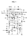
- Fig. 1 is a circuit diagram of the high-frequency circuit according to the present embodiment.
- the high-frequency circuit is disposed upstream of an input tuning circuit of a television tuner.
- a wideband amplifier 2 is connected to the high-frequency circuit in order to amplify a high-frequency signal input to an antenna connection terminal 1.
- a negative-feedback circuit 3 that attenuates a signal in a band lower than the reception band of the wideband amplifier 2 is connected to the wideband amplifier 2 in parallel.
- a bypass circuit 4 is connected to the wideband amplifier 2 in parallel.
- a switching circuit 5 is connected to the wideband amplifier 2 and the bypass circuit 4 so as to enable switching of a signal path between the wideband amplifier 2 and the bypass circuit 4.
- the wideband amplifier 2 includes a high-frequency amplifying transistor Tr.
- a signal is input to the base of the high-frequency amplifying transistor Tr from the antenna connection terminal 1 via a capacitor C1.
- a bias voltage is applied to the base of the high-frequency amplifying transistor Tr using resistors R1 and R2 of the negative-feedback circuit 3, which is connected between the base and a collector of the high-frequency amplifying transistor Tr, and a bias resistor R3.
- a capacitor C2 that allows a high-frequency component to pass therethrough is connected to the resistor R1 in parallel.
- An emitter of the high-frequency amplifying transistor Tr of the wideband amplifier 2 is connected to ground via a capacitor C3 and a resistor R4 for high frequencies.
- the emitter of the high-frequency amplifying transistor Tr is connected to a collector of a first switching transistor Trs1 of a switching circuit 5 via a bias resistor R5.
- the collector of the high-frequency amplifying transistor Tr outputs a signal to the next stage via a capacitor C4.
- bypass circuit 4 is connected between the base and the collector of the high-frequency amplifying transistor Tr of the wideband amplifier 2 in parallel.
- a first switching diode D1, a capacitor C5, a second switching diode D2, and a bias resistor R6 are connected in series in this order from the base side to the collector side.
- An anode of the first switching diode D1 and the anode of the second switching diode D2 are connected to the base and the collector of the high-frequency amplifying transistor Tr for a direct current, respectively.
- a capacitor C6 is connected to the bias resistor R6 in parallel.
- the switching circuit 5 includes two transistors, that is, the first switching transistor Trs1 and a second switching transistor Trs2.
- the two transistors are connected to each other so that the emitters of the first switching transistor Trs1 and the second switching transistor Trs2 are connected to ground and on and off states of the first switching transistor Trs1 and the second switching transistor Trs2 are mutually complementarily switched.
- Cathodes of the switching diodes D1 and D2 of the bypass circuit 4 are connected to the collector of the second switching transistor Trs2 via coils L1 and L2, respectively, which are inductor elements.
- the coils L1 and L2 are grounded for high frequencies via a capacitor C7.
- the capacitor C5 of the bypass circuit 4 and the two coils L1 and L2 form a highpass filter in one section.
- An AGC voltage obtained, for example, in accordance with the level of an input high-frequency signal is applied to the base of the first switching transistor Trs1 via bias resistors R7 and R8.
- the collector of the first switching transistor Trs1 is connected to the base of the second switching transistor Trs2 via a bias resistor R9.
- a power supply voltage Vcc is applied to the collectors of the first switching transistor Trs1 and the second switching transistor Trs2 via resistors R10 and R11, respectively.
- the power supply voltage Vcc is applied to the collector of the high-frequency amplifying transistor Tr via a resistor R12 and a coil L3.
- the middle point between the resistor R12 and the coil L3 is connected to ground for high frequencies.
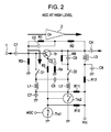
- Fig. 2 is an equivalent circuit diagram illustrating the operation of the high-frequency circuit shown in Fig. 1 when an input electric field is at a low level and the AGC voltage is at a high level.
- Fig. 3 is an equivalent circuit diagram illustrating the operation of the high-frequency circuit shown in Fig. 1 when the input electric field is at a high level and the AGC voltage is at a low level.
- the AGC voltage is used for increasing and decreasing the total gain of the amplifying stage of a receiver in accordance with the level of a reception signal.
- the AGC voltage is at a high level.
- the AGC voltage When the AGC voltage is at a high level, a voltage divided by the bias resistors R7 and R8 is applied to the base of the first switching transistor Trs1 of the switching circuit 5 so that the first switching transistor Trs1 is turned on. Accordingly, the collector voltage of the first switching transistor Trs1 becomes 0 V. Thus, the second switching transistor Trs2 is turned off. Since the bias resistor R5 connected to the emitter of the high-frequency amplifying transistor Tr of the wideband amplifier 2 is connected to ground via the first switching transistor Trs1, the high-frequency amplifying transistor Tr is turned on and the wideband amplifier 2 operates. Accordingly, a predetermined amplifying gain can be obtained and a signal is output to the next stage via the capacitor C4.
- the AGC voltage is used for increasing and decreasing the total gain of the amplifying stage of a receiver in accordance with the level of a reception signal.
- the AGC voltage is at a low level.
- a voltage applied to the base of the first switching transistor Trs1 of the switching circuit 5 is at a low level. Accordingly, the first switching transistor Trs1 is turned off. Since the power supply voltage Vcc is applied to the base of the second switching transistor Trs2 via the resistors R10 and R9, the second switching transistor Trs2 is turned on. A portion of a voltage divided between the resistor R9 and the resistor R10 (about 2 V) is applied to the emitter of the high-frequency amplifying transistor Tr of the wideband amplifier 2 via the bias resistor R5, which is connected to the emitter of the high-frequency amplifying transistor Tr.
- the second switching transistor Trs2 since the second switching transistor Trs2 is conductive, and therefore, the collector voltage of the second switching transistor Trs2 becomes 0 V, the first switching diode D1 and the second switching diode D2 are conductive. In addition, the base voltage of the high-frequency amplifying transistor Tr is decreased to about 0.7 V. Thus, the base voltage of the high-frequency amplifying transistor Tr of the wideband amplifier 2 is lower than the emitter voltage. Accordingly, the high-frequency amplifying transistor Tr is turned off, the wideband amplifier 2 is turned off, the bypass circuit 4 is conductive, and the input signal is output via the bypass circuit 4 and the capacitor C4.
- the bypass circuit functions as a filter. Therefore, the signal in a passband lower than the reception band can be reliably attenuated.
- the bypass circuit 4 functions as a filter when the bypass circuit 4 operates.
- the signal in a passband lower than the reception band of the bypass circuit 4 can be further attenuated.
Landscapes
- Engineering & Computer Science (AREA)
- Power Engineering (AREA)
- Networks Using Active Elements (AREA)
- Control Of Amplification And Gain Control (AREA)
- Input Circuits Of Receivers And Coupling Of Receivers And Audio Equipment (AREA)
- Amplifiers (AREA)
Abstract
Description
- The present invention relates to a high-frequency circuit and, in particular, to a high-frequency circuit including a wideband amplifier, a bypass circuit, and a switching circuit that switches between the wideband amplifier and the bypass circuit.
- In general, circuits, such as television tuners, that control a high-frequency signal appropriately perform signal processing in accordance with the level of an input electric field composed of a high-frequency signal.
- For example, a television tuner is described which includes a wideband amplifier and a bypass circuit upstream of an input tuning circuit and a switching circuit that switches between the wideband amplifier and the bypass circuit (refer to, for example,
Japanese Registered Utility Model No. 3099778 - This television tuner separately includes a filter circuit upstream of the wideband amplifier and the bypass circuit in order to attenuate a signal in a low band outside the input band.
- However, nowadays, with the widespread use of portable electronic devices, circuits need to be simplified, the size of circuits needs to be reduced, and circuits of high performance is required. The filter circuits separately provided upstream of the wideband amplifier and the bypass circuit do not meet these needs.
- Accordingly, a circuit is required that has a simplified configuration, reduced size, and increased performance while providing functionality that is the same as that of the filter circuit.
- It is known that the wideband amplifier can attenuate a signal in a band lower than the reception band by providing a negative-feedback circuit. However, the bypass circuit cannot provide a filter function.
- Accordingly, it is an object of the present invention to provide a high-frequency circuit including a wideband amplifier, a bypass circuit, and a switching circuit that switches between the wideband amplifier and the bypass circuit so as to attenuate a signal in a band lower than the reception band by causing the bypass circuit to function as a filter when the bypass circuit operates.
- According to an embodiment of the present invention, a high-frequency circuit includes a wideband amplifier for amplifying an input high-frequency signal, a bypass circuit having a capacitor and being connected to the wideband amplifier in parallel, and a switching circuit having an inductor and switching a path of the signal between a path in the wideband amplifier and a path in the bypass circuit. When the switching circuit switches the path of the signal to the path in the bypass circuit, the capacitor and the inductor form a highpass filter.
- In the high-frequency circuit, when the switching circuit switches the path of the signal to the path in the bypass circuit, the capacitor included in the bypass circuit and the inductor included in the switching circuit form a highpass filter. Accordingly, only an appropriate signal can be output to the next stage, and therefore, a signal in a band lower than the reception band of the bypass circuit can be further attenuated.
- In the high-frequency circuit, the wideband amplifier can include a high-frequency transistor, the bypass circuit can include at least a diode in a stage upstream of the capacitor, one end of the diode in the stage upstream of the capacitor can be connected to the base of the high-frequency transistor, and the switching circuit can include a switching transistor. The inductor can be disposed between the switching transistor and the diode, a switching voltage can be applied to the diode and the high-frequency transistor via the switching transistor and the inductor, and the diode and the high-frequency transistor can be switched on and off by switching on and off the switching transistor.
- The high-frequency circuit can cause the diode in the bypass circuit and the high-frequency transistor in the wideband amplifier to be switched on and off by switching on and off the switching transistor in the switching circuit. Thus, when the bypass filter is turned on, the capacitor and the inductor form a high-pass filter. Accordingly, only an appropriate signal can be output to the next stage, and therefore, a signal in a band lower than the reception band of the bypass circuit can be further attenuated.
- In the high-frequency circuit, the bypass circuit can include a diode in each of the stages upstream and downstream of the capacitor, the switching circuit can include two switching transistors, and two switching transistors can be connected to each other so that the emitters of the two switching transistors are connected to ground and the two switching transistors are mutually complementarily switched on and off. An AGC voltage obtained in accordance with the level of the input high-frequency signal can be input to the base of one of the two switching transistors, and an inductor can be connected between the collector of the other switching transistor and each of the two diodes. When the switching transistor connected to the inductor is switched on, the path of the signal can be switched to the bypass circuit and the capacitor and the two inductors can form a highpass filter in one section.
- In the high-frequency circuit, when an AGC voltage applied to the switching circuit is at a high level, the two diodes of the bypass circuit are turned off, and therefore, the bypass circuit is turned off. In addition, the wideband amplifier is turned on. When the AGC voltage applied to the switching circuit is at a low level, the switching transistor connected to the inductor is turned on, and the two diodes of the bypass circuit are turned on. Therefore, the bypass circuit is turned on. In addition, the wideband amplifier is turned off. Thus, the path of a signal is switched to the path in the bypass circuit, and the capacitor and the two inductors form a highpass filter in one section. Accordingly, a signal in a band lower than the reception band of the bypass circuit can be further attenuated.
- In the high-frequency circuit, the wideband amplifier can include a negative-feedback circuit and the negative-feedback circuit can attenuate a signal in a band lower than a reception band of the wideband amplifier.
- Since the high-frequency circuit includes a negative-feedback circuit, the high-frequency circuit can attenuate a signal in a band lower than a reception band of the wideband amplifier.
- As described above, according to the present invention, a high-frequency circuit includes a wideband amplifier and a bypass circuit, and a switching circuit that switches between the wideband amplifier and the bypass circuit. In this way, a high-frequency circuit that can attenuate a signal in a band lower than the reception band can be provided by causing the bypass circuit to function as a filter when the bypass circuit operates.
-
- Fig. 1 is a circuit diagram of a high-frequency circuit according to an embodiment of the present invention;
- Fig. 2 is an equivalent circuit diagram illustrating the operation of the high-frequency circuit shown in Fig. 1 when an input electric field is at a low level and the AGC voltage is at a high level; and
- Fig. 3 is an equivalent circuit diagram illustrating the operation of the high-frequency circuit shown in Fig. 1 when an input electric field is at a high level and the AGC voltage is at a low level.
- A high-frequency circuit according to an embodiment of the present invention is now herein described with reference to Figs. 1 to 3.
- Fig. 1 is a circuit diagram of the high-frequency circuit according to the present embodiment.
- As shown in Fig. 1, according to the present embodiment, the high-frequency circuit is disposed upstream of an input tuning circuit of a television tuner. A
wideband amplifier 2 is connected to the high-frequency circuit in order to amplify a high-frequency signal input to anantenna connection terminal 1. A negative-feedback circuit 3 that attenuates a signal in a band lower than the reception band of thewideband amplifier 2 is connected to thewideband amplifier 2 in parallel. In addition, a bypass circuit 4 is connected to thewideband amplifier 2 in parallel. Furthermore, a switching circuit 5 is connected to thewideband amplifier 2 and the bypass circuit 4 so as to enable switching of a signal path between thewideband amplifier 2 and the bypass circuit 4. - The configuration is described below in more detail. The
wideband amplifier 2 includes a high-frequency amplifying transistor Tr. A signal is input to the base of the high-frequency amplifying transistor Tr from theantenna connection terminal 1 via a capacitor C1. A bias voltage is applied to the base of the high-frequency amplifying transistor Tr using resistors R1 and R2 of the negative-feedback circuit 3, which is connected between the base and a collector of the high-frequency amplifying transistor Tr, and a bias resistor R3. A capacitor C2 that allows a high-frequency component to pass therethrough is connected to the resistor R1 in parallel. An emitter of the high-frequency amplifying transistor Tr of thewideband amplifier 2 is connected to ground via a capacitor C3 and a resistor R4 for high frequencies. In addition, the emitter of the high-frequency amplifying transistor Tr is connected to a collector of a first switching transistor Trs1 of a switching circuit 5 via a bias resistor R5. The collector of the high-frequency amplifying transistor Tr outputs a signal to the next stage via a capacitor C4. - In addition, the bypass circuit 4 is connected between the base and the collector of the high-frequency amplifying transistor Tr of the
wideband amplifier 2 in parallel. In the bypass circuit 4, a first switching diode D1, a capacitor C5, a second switching diode D2, and a bias resistor R6 are connected in series in this order from the base side to the collector side. An anode of the first switching diode D1 and the anode of the second switching diode D2 are connected to the base and the collector of the high-frequency amplifying transistor Tr for a direct current, respectively. A capacitor C6 is connected to the bias resistor R6 in parallel. - In addition, the switching circuit 5 includes two transistors, that is, the first switching transistor Trs1 and a second switching transistor Trs2. The two transistors are connected to each other so that the emitters of the first switching transistor Trs1 and the second switching transistor Trs2 are connected to ground and on and off states of the first switching transistor Trs1 and the second switching transistor Trs2 are mutually complementarily switched. Cathodes of the switching diodes D1 and D2 of the bypass circuit 4 are connected to the collector of the second switching transistor Trs2 via coils L1 and L2, respectively, which are inductor elements. The coils L1 and L2 are grounded for high frequencies via a capacitor C7. When the second switching transistor Trs2 is turned on and a signal path is switched to a path in the bypass circuit 4, the capacitor C5 of the bypass circuit 4 and the two coils L1 and L2 form a highpass filter in one section. An AGC voltage obtained, for example, in accordance with the level of an input high-frequency signal is applied to the base of the first switching transistor Trs1 via bias resistors R7 and R8. The collector of the first switching transistor Trs1 is connected to the base of the second switching transistor Trs2 via a bias resistor R9. A power supply voltage Vcc is applied to the collectors of the first switching transistor Trs1 and the second switching transistor Trs2 via resistors R10 and R11, respectively.
- Additionally, the power supply voltage Vcc is applied to the collector of the high-frequency amplifying transistor Tr via a resistor R12 and a coil L3. The middle point between the resistor R12 and the coil L3 is connected to ground for high frequencies.
- The operation of the present embodiment is described next with reference to Figs. 2 and 3.
- Fig. 2 is an equivalent circuit diagram illustrating the operation of the high-frequency circuit shown in Fig. 1 when an input electric field is at a low level and the AGC voltage is at a high level. In contrast, Fig. 3 is an equivalent circuit diagram illustrating the operation of the high-frequency circuit shown in Fig. 1 when the input electric field is at a high level and the AGC voltage is at a low level.
- The AGC voltage is used for increasing and decreasing the total gain of the amplifying stage of a receiver in accordance with the level of a reception signal. When the input electric field is at a low level, the AGC voltage is at a high level.
- When the AGC voltage is at a high level, a voltage divided by the bias resistors R7 and R8 is applied to the base of the first switching transistor Trs1 of the switching circuit 5 so that the first switching transistor Trs1 is turned on. Accordingly, the collector voltage of the first switching transistor Trs1 becomes 0 V. Thus, the second switching transistor Trs2 is turned off. Since the bias resistor R5 connected to the emitter of the high-frequency amplifying transistor Tr of the
wideband amplifier 2 is connected to ground via the first switching transistor Trs1, the high-frequency amplifying transistor Tr is turned on and thewideband amplifier 2 operates. Accordingly, a predetermined amplifying gain can be obtained and a signal is output to the next stage via the capacitor C4. Since the power supply voltage Vcc is applied to the cathodes of the first switching diode D1 and the second switching diode D2 of the bias circuit via the coils L1 and L2 of the switching circuit 5, respectively, the switching diodes D1 and D2 are open, and therefore, the bypass circuit 4 does not operate. - The AGC voltage is used for increasing and decreasing the total gain of the amplifying stage of a receiver in accordance with the level of a reception signal. When the input electric field is at a high level, the AGC voltage is at a low level.
- When the AGC voltage is at a low level, a voltage applied to the base of the first switching transistor Trs1 of the switching circuit 5 is at a low level. Accordingly, the first switching transistor Trs1 is turned off. Since the power supply voltage Vcc is applied to the base of the second switching transistor Trs2 via the resistors R10 and R9, the second switching transistor Trs2 is turned on. A portion of a voltage divided between the resistor R9 and the resistor R10 (about 2 V) is applied to the emitter of the high-frequency amplifying transistor Tr of the
wideband amplifier 2 via the bias resistor R5, which is connected to the emitter of the high-frequency amplifying transistor Tr. In addition, since the second switching transistor Trs2 is conductive, and therefore, the collector voltage of the second switching transistor Trs2 becomes 0 V, the first switching diode D1 and the second switching diode D2 are conductive. In addition, the base voltage of the high-frequency amplifying transistor Tr is decreased to about 0.7 V. Thus, the base voltage of the high-frequency amplifying transistor Tr of thewideband amplifier 2 is lower than the emitter voltage. Accordingly, the high-frequency amplifying transistor Tr is turned off, thewideband amplifier 2 is turned off, the bypass circuit 4 is conductive, and the input signal is output via the bypass circuit 4 and the capacitor C4. At that time, by setting the function of the highpass filter formed by the coils L1 and L2 of the switching circuit and the capacitor C5 of the bypass circuit 4 to a value that attenuates the signal in a passband lower than the reception band, the bypass circuit functions as a filter. Therefore, the signal in a passband lower than the reception band can be reliably attenuated. - Consequently, according to the present embodiment, by providing the
wideband amplifier 2 and the bypass circuit 4 and further providing the switching circuit 5 that switches between thewideband amplifier 2 and the bypass circuit 4, the bypass circuit 4 functions as a filter when the bypass circuit 4 operates. Thus, the signal in a passband lower than the reception band of the bypass circuit 4 can be further attenuated. - It should be understood that the present invention is not limited to the particular embodiments described herein, but is intended to include all changes and modifications that are within the scope and spirit of the invention as set forth in the claims.
Claims (4)
- A high-frequency circuit comprising:a wideband amplifier for amplifying an input high-frequency signal;a bypass circuit having a capacitor, the bypass circuit being connected to the wideband amplifier in parallel; anda switching circuit having an inductor, the switching circuit switching a path of the signal between a path in the wideband amplifier and a path in the bypass circuit;wherein, when the switching circuit switches the path of the signal to the path in the bypass circuit, the capacitor and the inductor form a highpass filter.
- The high-frequency circuit according to Claim 1, wherein the wideband amplifier includes a high-frequency transistor, the bypass circuit includes at least a diode in a stage upstream of the capacitor, one end of the diode in the stage upstream of the capacitor is connected to the base of the high-frequency transistor, and the switching circuit includes a switching transistor, and wherein the inductor is disposed between the switching transistor and the diode, a switching voltage is applied to the diode and the high-frequency transistor via the switching transistor and the inductor, and the diode and the high-frequency transistor are switched on and off by switching on and off the switching transistor.
- The high-frequency circuit according to Claim 1 or 2, wherein the bypass circuit includes a diode in each of the stages upstream and downstream of the capacitor, the switching circuit includes two switching transistors, and the two switching transistors are connected to each other so that the emitters of the two switching transistors are connected to ground and the two switching transistors are mutually complementarily switched on and off, and wherein an AGC voltage obtained in accordance with the level of the input high-frequency signal is input to the base of one of the two switching transistors, and an inductor is connected between the collector of the other switching transistor and each of the two diodes, and wherein, when the switching transistor connected to the inductors is switched on, the path of the signal is switched to the bypass circuit and the capacitor and the two inductors form a highpass filter in one section.
- The high-frequency circuit according to any one of Claims 1 to 3, wherein the wideband amplifier includes a negative-feedback circuit and the negative-feedback circuit attenuates a signal in a band lower than a reception band of the wideband amplifier.
Applications Claiming Priority (1)
| Application Number | Priority Date | Filing Date | Title |
|---|---|---|---|
| JP2006123536A JP2007295480A (en) | 2006-04-27 | 2006-04-27 | High frequency circuit |
Publications (1)
| Publication Number | Publication Date |
|---|---|
| EP1850472A1 true EP1850472A1 (en) | 2007-10-31 |
Family
ID=38222405
Family Applications (1)
| Application Number | Title | Priority Date | Filing Date |
|---|---|---|---|
| EP07008426A Withdrawn EP1850472A1 (en) | 2006-04-27 | 2007-04-25 | High-frequency circuit |
Country Status (2)
| Country | Link |
|---|---|
| EP (1) | EP1850472A1 (en) |
| JP (1) | JP2007295480A (en) |
Cited By (5)
| Publication number | Priority date | Publication date | Assignee | Title |
|---|---|---|---|---|
| KR101101504B1 (en) | 2009-07-09 | 2012-01-03 | 삼성전기주식회사 | Path switchable amplifier circuit |
| DE102008062308B4 (en) * | 2008-06-12 | 2012-04-19 | Mitsubishi Electric Corp. | power amplifier |
| CN116388716A (en) * | 2023-06-02 | 2023-07-04 | 睿思芯科(深圳)技术有限公司 | Radio frequency low noise amplifier and radio frequency chip |
| US12067481B2 (en) | 2018-10-14 | 2024-08-20 | International Business Machines Corporation | Array-integrated upstream/downstream router for circuit switched parallel connectivity |
| US12518149B2 (en) | 2021-09-29 | 2026-01-06 | International Business Machines Corporation | Implicit vector concatenation within 2D mesh routing |
Citations (3)
| Publication number | Priority date | Publication date | Assignee | Title |
|---|---|---|---|---|
| US5909643A (en) * | 1995-11-24 | 1999-06-01 | Matsushita Electric Industrial Co., Ltd. | Transmitter power varying device having a bypass line for a power amplifier |
| US20030112065A1 (en) * | 2001-12-13 | 2003-06-19 | Edward Russel Brown | Low noise amplifier circuit wih phase matched switch topology |
| US20040124917A1 (en) * | 2002-12-12 | 2004-07-01 | New Japan Radio Co., Ltd. | Variable gain amplifier |
Family Cites Families (3)
| Publication number | Priority date | Publication date | Assignee | Title |
|---|---|---|---|---|
| WO1990014718A1 (en) * | 1989-05-18 | 1990-11-29 | Motorola, Inc. | Method and apparatus for reducing intermodulation distortion |
| JPH0821874B2 (en) * | 1990-06-25 | 1996-03-04 | セイコー電子工業株式会社 | Wireless communication equipment |
| US6253070B1 (en) * | 1998-07-22 | 2001-06-26 | Denso Corporation | Diode amplifier bypass circuit |
-
2006
- 2006-04-27 JP JP2006123536A patent/JP2007295480A/en not_active Ceased
-
2007
- 2007-04-25 EP EP07008426A patent/EP1850472A1/en not_active Withdrawn
Patent Citations (3)
| Publication number | Priority date | Publication date | Assignee | Title |
|---|---|---|---|---|
| US5909643A (en) * | 1995-11-24 | 1999-06-01 | Matsushita Electric Industrial Co., Ltd. | Transmitter power varying device having a bypass line for a power amplifier |
| US20030112065A1 (en) * | 2001-12-13 | 2003-06-19 | Edward Russel Brown | Low noise amplifier circuit wih phase matched switch topology |
| US20040124917A1 (en) * | 2002-12-12 | 2004-07-01 | New Japan Radio Co., Ltd. | Variable gain amplifier |
Cited By (6)
| Publication number | Priority date | Publication date | Assignee | Title |
|---|---|---|---|---|
| DE102008062308B4 (en) * | 2008-06-12 | 2012-04-19 | Mitsubishi Electric Corp. | power amplifier |
| KR101101504B1 (en) | 2009-07-09 | 2012-01-03 | 삼성전기주식회사 | Path switchable amplifier circuit |
| US12067481B2 (en) | 2018-10-14 | 2024-08-20 | International Business Machines Corporation | Array-integrated upstream/downstream router for circuit switched parallel connectivity |
| US12518149B2 (en) | 2021-09-29 | 2026-01-06 | International Business Machines Corporation | Implicit vector concatenation within 2D mesh routing |
| CN116388716A (en) * | 2023-06-02 | 2023-07-04 | 睿思芯科(深圳)技术有限公司 | Radio frequency low noise amplifier and radio frequency chip |
| CN116388716B (en) * | 2023-06-02 | 2023-08-29 | 睿思芯科(深圳)技术有限公司 | Radio frequency low noise amplifier and radio frequency chip |
Also Published As
| Publication number | Publication date |
|---|---|
| JP2007295480A (en) | 2007-11-08 |
Similar Documents
| Publication | Publication Date | Title |
|---|---|---|
| US8217723B2 (en) | Low noise amplifier circuit | |
| US8149049B2 (en) | Low noise receiving apparatus | |
| US6522195B2 (en) | Low noise amplifier having bypass circuitry | |
| CN101515784B (en) | Amplifier, attenuation module and method for attenuating radio frequency signals | |
| EP0886384A2 (en) | Single-stage dual-band low-noise amplifier for use in a wireless communication system receiver | |
| US7667541B2 (en) | Amplifier circuit and wireless communication device | |
| CN111988004B (en) | Amplifying circuit, high-frequency front-end circuit, and communication device | |
| US9742364B2 (en) | System and method for a low noise amplifier module | |
| US6630861B2 (en) | Variable gain amplifier | |
| CN115088190A (en) | Power amplifying circuit, high frequency circuit and communication device | |
| JPH0117855Y2 (en) | ||
| GB2314223A (en) | A low noise, high frequency, amplifier using a common base input stage and a White's cascode output stage | |
| CN115812276A (en) | High frequency circuit and communication device | |
| JP3596361B2 (en) | Amplifier bypass circuit with diode | |
| US6900850B2 (en) | Television tuner having simplified wiring for interconnection and having miniaturized integrated circuit | |
| JP2007295480A (en) | High frequency circuit | |
| US7412219B2 (en) | High-frequency amplifier having simple circuit structure and television tuner using high-frequency amplifier | |
| US7345556B2 (en) | Variable attenuation circuit having large attenuation amount with small circuit size | |
| JP3806617B2 (en) | Television tuner | |
| WO2021256088A1 (en) | High frequency circuit, and communication device | |
| JP3108712U (en) | Variable gain amplifier circuit | |
| JP2013131802A (en) | Rf power amplifier and method of operating the same | |
| JP3745949B2 (en) | Television tuner | |
| KR100764373B1 (en) | TV receiver with low noise AFC function | |
| KR0117516Y1 (en) | Power supply circuits |
Legal Events
| Date | Code | Title | Description |
|---|---|---|---|
| PUAI | Public reference made under article 153(3) epc to a published international application that has entered the european phase |
Free format text: ORIGINAL CODE: 0009012 |
|
| AK | Designated contracting states |
Kind code of ref document: A1 Designated state(s): AT BE BG CH CY CZ DE DK EE ES FI FR GB GR HU IE IS IT LI LT LU LV MC MT NL PL PT RO SE SI SK TR |
|
| AX | Request for extension of the european patent |
Extension state: AL BA HR MK YU |
|
| 17P | Request for examination filed |
Effective date: 20070925 |
|
| 17Q | First examination report despatched |
Effective date: 20071214 |
|
| GRAP | Despatch of communication of intention to grant a patent |
Free format text: ORIGINAL CODE: EPIDOSNIGR1 |
|
| AKX | Designation fees paid |
Designated state(s): DE FR GB |
|
| GRAS | Grant fee paid |
Free format text: ORIGINAL CODE: EPIDOSNIGR3 |
|
| GRAJ | Information related to disapproval of communication of intention to grant by the applicant or resumption of examination proceedings by the epo deleted |
Free format text: ORIGINAL CODE: EPIDOSDIGR1 |
|
| GRAL | Information related to payment of fee for publishing/printing deleted |
Free format text: ORIGINAL CODE: EPIDOSDIGR3 |
|
| GRAP | Despatch of communication of intention to grant a patent |
Free format text: ORIGINAL CODE: EPIDOSNIGR1 |
|
| STAA | Information on the status of an ep patent application or granted ep patent |
Free format text: STATUS: THE APPLICATION IS DEEMED TO BE WITHDRAWN |
|
| 18D | Application deemed to be withdrawn |
Effective date: 20091111 |