EP1850381A2 - Mounting substrate - Google Patents
Mounting substrate Download PDFInfo
- Publication number
- EP1850381A2 EP1850381A2 EP07008530A EP07008530A EP1850381A2 EP 1850381 A2 EP1850381 A2 EP 1850381A2 EP 07008530 A EP07008530 A EP 07008530A EP 07008530 A EP07008530 A EP 07008530A EP 1850381 A2 EP1850381 A2 EP 1850381A2
- Authority
- EP
- European Patent Office
- Prior art keywords
- mounting substrate
- connection pads
- insulation layer
- semiconductor chip
- connection
- Prior art date
- Legal status (The legal status is an assumption and is not a legal conclusion. Google has not performed a legal analysis and makes no representation as to the accuracy of the status listed.)
- Withdrawn
Links
Images


Classifications
-
- H—ELECTRICITY
- H05—ELECTRIC TECHNIQUES NOT OTHERWISE PROVIDED FOR
- H05K—PRINTED CIRCUITS; CASINGS OR CONSTRUCTIONAL DETAILS OF ELECTRIC APPARATUS; MANUFACTURE OF ASSEMBLAGES OF ELECTRICAL COMPONENTS
- H05K1/00—Printed circuits
- H05K1/02—Details
- H05K1/11—Printed elements for providing electric connections to or between printed circuits
- H05K1/111—Pads for surface mounting, e.g. lay-out
-
- H—ELECTRICITY
- H01—ELECTRIC ELEMENTS
- H01L—SEMICONDUCTOR DEVICES NOT COVERED BY CLASS H10
- H01L23/00—Details of semiconductor or other solid state devices
- H01L23/48—Arrangements for conducting electric current to or from the solid state body in operation, e.g. leads, terminal arrangements ; Selection of materials therefor
- H01L23/488—Arrangements for conducting electric current to or from the solid state body in operation, e.g. leads, terminal arrangements ; Selection of materials therefor consisting of soldered or bonded constructions
- H01L23/498—Leads, i.e. metallisations or lead-frames on insulating substrates, e.g. chip carriers
- H01L23/49811—Additional leads joined to the metallisation on the insulating substrate, e.g. pins, bumps, wires, flat leads
- H01L23/49816—Spherical bumps on the substrate for external connection, e.g. ball grid arrays [BGA]
-
- H—ELECTRICITY
- H01—ELECTRIC ELEMENTS
- H01L—SEMICONDUCTOR DEVICES NOT COVERED BY CLASS H10
- H01L23/00—Details of semiconductor or other solid state devices
- H01L23/48—Arrangements for conducting electric current to or from the solid state body in operation, e.g. leads, terminal arrangements ; Selection of materials therefor
- H01L23/488—Arrangements for conducting electric current to or from the solid state body in operation, e.g. leads, terminal arrangements ; Selection of materials therefor consisting of soldered or bonded constructions
- H01L23/498—Leads, i.e. metallisations or lead-frames on insulating substrates, e.g. chip carriers
- H01L23/49838—Geometry or layout
-
- H—ELECTRICITY
- H01—ELECTRIC ELEMENTS
- H01L—SEMICONDUCTOR DEVICES NOT COVERED BY CLASS H10
- H01L23/00—Details of semiconductor or other solid state devices
- H01L23/48—Arrangements for conducting electric current to or from the solid state body in operation, e.g. leads, terminal arrangements ; Selection of materials therefor
- H01L23/488—Arrangements for conducting electric current to or from the solid state body in operation, e.g. leads, terminal arrangements ; Selection of materials therefor consisting of soldered or bonded constructions
- H01L23/498—Leads, i.e. metallisations or lead-frames on insulating substrates, e.g. chip carriers
- H01L23/49822—Multilayer substrates
-
- H—ELECTRICITY
- H01—ELECTRIC ELEMENTS
- H01L—SEMICONDUCTOR DEVICES NOT COVERED BY CLASS H10
- H01L2924/00—Indexing scheme for arrangements or methods for connecting or disconnecting semiconductor or solid-state bodies as covered by H01L24/00
- H01L2924/0001—Technical content checked by a classifier
- H01L2924/0002—Not covered by any one of groups H01L24/00, H01L24/00 and H01L2224/00
-
- H—ELECTRICITY
- H05—ELECTRIC TECHNIQUES NOT OTHERWISE PROVIDED FOR
- H05K—PRINTED CIRCUITS; CASINGS OR CONSTRUCTIONAL DETAILS OF ELECTRIC APPARATUS; MANUFACTURE OF ASSEMBLAGES OF ELECTRICAL COMPONENTS
- H05K2201/00—Indexing scheme relating to printed circuits covered by H05K1/00
- H05K2201/09—Shape and layout
- H05K2201/09209—Shape and layout details of conductors
- H05K2201/09218—Conductive traces
- H05K2201/09227—Layout details of a plurality of traces, e.g. escape layout for Ball Grid Array [BGA] mounting
-
- H—ELECTRICITY
- H05—ELECTRIC TECHNIQUES NOT OTHERWISE PROVIDED FOR
- H05K—PRINTED CIRCUITS; CASINGS OR CONSTRUCTIONAL DETAILS OF ELECTRIC APPARATUS; MANUFACTURE OF ASSEMBLAGES OF ELECTRICAL COMPONENTS
- H05K2201/00—Indexing scheme relating to printed circuits covered by H05K1/00
- H05K2201/09—Shape and layout
- H05K2201/09209—Shape and layout details of conductors
- H05K2201/09372—Pads and lands
- H05K2201/094—Array of pads or lands differing from one another, e.g. in size, pitch, thickness; Using different connections on the pads
-
- H—ELECTRICITY
- H05—ELECTRIC TECHNIQUES NOT OTHERWISE PROVIDED FOR
- H05K—PRINTED CIRCUITS; CASINGS OR CONSTRUCTIONAL DETAILS OF ELECTRIC APPARATUS; MANUFACTURE OF ASSEMBLAGES OF ELECTRICAL COMPONENTS
- H05K2201/00—Indexing scheme relating to printed circuits covered by H05K1/00
- H05K2201/09—Shape and layout
- H05K2201/09818—Shape or layout details not covered by a single group of H05K2201/09009 - H05K2201/09809
- H05K2201/0989—Coating free areas, e.g. areas other than pads or lands free of solder resist
-
- H—ELECTRICITY
- H05—ELECTRIC TECHNIQUES NOT OTHERWISE PROVIDED FOR
- H05K—PRINTED CIRCUITS; CASINGS OR CONSTRUCTIONAL DETAILS OF ELECTRIC APPARATUS; MANUFACTURE OF ASSEMBLAGES OF ELECTRICAL COMPONENTS
- H05K2201/00—Indexing scheme relating to printed circuits covered by H05K1/00
- H05K2201/09—Shape and layout
- H05K2201/09818—Shape or layout details not covered by a single group of H05K2201/09009 - H05K2201/09809
- H05K2201/099—Coating over pads, e.g. solder resist partly over pads
-
- H—ELECTRICITY
- H05—ELECTRIC TECHNIQUES NOT OTHERWISE PROVIDED FOR
- H05K—PRINTED CIRCUITS; CASINGS OR CONSTRUCTIONAL DETAILS OF ELECTRIC APPARATUS; MANUFACTURE OF ASSEMBLAGES OF ELECTRICAL COMPONENTS
- H05K2201/00—Indexing scheme relating to printed circuits covered by H05K1/00
- H05K2201/10—Details of components or other objects attached to or integrated in a printed circuit board
- H05K2201/10613—Details of electrical connections of non-printed components, e.g. special leads
- H05K2201/10621—Components characterised by their electrical contacts
- H05K2201/10674—Flip chip
-
- H—ELECTRICITY
- H05—ELECTRIC TECHNIQUES NOT OTHERWISE PROVIDED FOR
- H05K—PRINTED CIRCUITS; CASINGS OR CONSTRUCTIONAL DETAILS OF ELECTRIC APPARATUS; MANUFACTURE OF ASSEMBLAGES OF ELECTRICAL COMPONENTS
- H05K3/00—Apparatus or processes for manufacturing printed circuits
- H05K3/30—Assembling printed circuits with electric components, e.g. with resistor
- H05K3/32—Assembling printed circuits with electric components, e.g. with resistor electrically connecting electric components or wires to printed circuits
- H05K3/34—Assembling printed circuits with electric components, e.g. with resistor electrically connecting electric components or wires to printed circuits by soldering
- H05K3/3452—Solder masks
-
- Y—GENERAL TAGGING OF NEW TECHNOLOGICAL DEVELOPMENTS; GENERAL TAGGING OF CROSS-SECTIONAL TECHNOLOGIES SPANNING OVER SEVERAL SECTIONS OF THE IPC; TECHNICAL SUBJECTS COVERED BY FORMER USPC CROSS-REFERENCE ART COLLECTIONS [XRACs] AND DIGESTS
- Y02—TECHNOLOGIES OR APPLICATIONS FOR MITIGATION OR ADAPTATION AGAINST CLIMATE CHANGE
- Y02P—CLIMATE CHANGE MITIGATION TECHNOLOGIES IN THE PRODUCTION OR PROCESSING OF GOODS
- Y02P70/00—Climate change mitigation technologies in the production process for final industrial or consumer products
- Y02P70/50—Manufacturing or production processes characterised by the final manufactured product
Definitions
- the present disclosure generally relates to substrates. In particular, it relates to substrates for mounting a semiconductor chip and to mounting of semiconductor chips on substrates.
- the present disclosure relates to a mounting substrate on which a semiconductor chip is mounted using a flip chip bonding. Specifically, it relates to a mounting substrate.
- a method of mounting a semiconductor chip on a mounting substrate using the flip chip bonding is characteristic in that a package can easily be made small in size and thin in thickness.
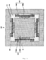
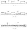
- Fig. 1 is a plan view showing an example of a configuration of a mounting substrate on which a semiconductor chip is mounted using the flip chip bonding.
- connection pads 13 are formed on an insulation layer 11 for connection to a semiconductor chip.
- a solder resist layer 12 having a opening 14 through which the connection pads 13 are exposed is formed on the insulation layer 11.
- the solder resist layer 12 is made up of solder resist layers 12A, 12B which are formed to be separated from each other across the opening 14. In this case, ends of the connection pads 13 are constructed to be covered by the solder resist layers 12A, 12B, respectively.
- a semiconductor chip 15 (as a matter of convenience in drawing, only briefly indicated by dotted lines for the sake of easy identification), which is to be mounted on the mounting substrate 10, is mounted thereon so that connecting portions (not shown) such as solder bumps which are formed on electrodes of the semiconductor chip 15 are brought into electrical connection with the connection pads 13.
- a resin referred to as an underfill is infiltrated between the semiconductor chip 15 and the mounting substrate 10, so as to realize an insulation between the adjacent connecting portions (connection pads).
- an underfill is infiltrated between the semiconductor chip 15 and the mounting substrate 10, so as to realize an insulation between the adjacent connecting portions (connection pads).
- Fig. 2 is an enlarged view of a portion lying in the vicinity of a corner portion of the mounting substrate 10 shown in Fig. 1. Note that, however, like reference numerals will be given to those that have already been described before, so that the description thereof will be omitted.
- the connection pads 13 As the number of pins to be placed increases, the intervals at which the connection pads 13 are placed become narrower in association therewith, and furthermore, the connection pads 13 have to also be formed even in areas closer to the corner portions of the mounting substrate 10. As this occurs, as is shown in Fig. 2, the connection pads come to interfere with each other in the corner portion of the mounting substrate 10, leading to a problem that the placement of the connection pads becomes difficult, in particular, in the corner portions.
- embodiments of the present invention provide a mounting substrate which can deal with the trend of narrowing the intervals at which the connecting portions are placed on the semiconductor chip which is mounted on the mounting substrate.
- a mounting substrate on which a semiconductor chip is mounted using a flip chip bonding comprises a plurality of connection pads to be connected to the semiconductor chip, and an insulation layer formed in such a manner as to cover the connection pads partially, wherein the insulation layer includes a first insulation layer which is formed in such a manner as to correspond to a center of the semiconductor chip and a second insulation layer which is formed in such a manner as to surround the first insulation layer, and wherein the plurality of connection pads include first connection pads which are partially covered by the first insulation layer and second connection pads which are partially covered by the second insulation layer.
- the mounting substrate which can deal with the trend of narrowing the intervals at which the connecting portions are placed on the semiconductor chip which is mounted on the mounting substrate.
- the insulation layer may be made up of a solder resist layer.
- first insulation layer may be formed into a quadrangle
- second connection pads may be placed in the vicinity of corner portions of the quadrangle, whereby the mutual interference of the connection pads in the vicinity of the corner portions can be suppressed effectively.
- connection pads which are exposed from an opening formed in the first insulation layer
- a semiconductor chip having connection pads at its central portion can be mounted.
- One or more embodiments of the present invention may include one or more the following advantages. For example, it becomes possible to provide the mounting substrate which can deal with the trend of narrowing the intervals at which the connecting portions are placed on the semiconductor chip which is mounted on the mounting substrate.
- the mounting substrate has both the first connection pads which are partially covered by the first insulation layer and the second connection pads which are partially covered by the second insulation layer. Because of this, the first connection pads or the second connection pads can be disposed in such a manner as to be connected to the connecting portions of the semiconductor chip which are placed at narrower intervals.
- the second connection pads are disposed in the vicinity of the corner portions of the first insulation layer formed which is formed substantially into the quadrangle so as to match the semiconductor chip which is also formed substantially into a quadrangle as viewed from the top thereof, thereby making it possible to avoid the interference of the connection pads.
- both the first connection pads and the second connection pads are formed, there is provided an advantage that the degree of freedom in laying out a connection path using the connection pads is increased.
- Embodiments according to the invention are also directed to methods by which the described apparatus is manufactured. It may include method steps for manufacturing parts of the apparatus. The method steps may be performed by way of hardware components, firmware, a computer programmed by appropriate software, by any combination thereof or in any other manner.
- Fig. 1 is a drawing which shows a related-art mounting substrate.
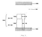
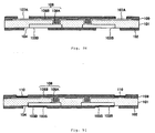
- Fig. 3 is a plan view showing exemplarily a mounting substrate 100 according to a first embodiment of the invention.
- the mounting substrate 100 shown in the figure has a construction in which connection pads 103 adapted to be connected to a semiconductor chip are formed on an insulation layer 101.
- the connection pads 103 are covered partially by an insulation layer (a solder resist layer) 102 which is formed on the insulation layer 101.
- the solder resist layer is formed into a solder resist layer 102A and a solder resist layer 102B which are separated from each other across an opening 140.
- the solder resist layer 102B is formed so as to mach the shape of the semiconductor chip and is formed into, for example, a quadrangular shape as viewed from the top thereof.
- the solder resist layer 102A is formed so as to surround the solder resist layer 102B.
- connection pads 103 are formed on the insulation layer 101 in such a manner as to be partially exposed from the opening 104.
- the connection pads 103 are configured so as to include connection pads 103A which are covered by the solder resist layer 102A at end portions thereof and connection pads 103B which are covered by the solder resist layer 102B at end portions thereof.
- connection pads which are connected to the semiconductor chip are configured so as to include the connection pads 103B which are covered by the solder resist layer 102B which is formed at a central portion of the mounting substrate and the connection pads 103A which are covered by the solder resist layer 102A which is formed at a circumferential edge portion of the mounting substrate.
- connection pads 103A and the connection pads 103B can be disposed at narrow intervals while avoiding the interference therebetween. Consequently, the semiconductor chip in which the connecting portions are placed at narrower intervals (that is, more pins are placed) can easily be mounted on the mounting substrate.
- connection pads 103A which are covered by the solder resist layer 102A at the end portions (or whose end portions are extended towards a circumferential edge portion of the mounting substrate) are placed in the vicinity of corner portions of the mounting substrate 100 (or in the vicinity of corner portions of the solder resist layer 102B).
- the connection pads 103A are formed in such a manner as not to be brought into contact with the solder resist layer 102B.
- the plurality of connection pads 103A can be placed without any interference therebetween. Because of this, it is seen that the mounting substrate 100 is constructed such that the semiconductor chip in which the connecting portions are placed at narrower intervals can easily be mounted thereon.
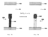
- Fig. 4 is an enlarged view which shows a state in which the connection pad 103A is placed.
- the connection pad 103A which is covered by the solder resist layer 102A at the end portion thereof has a construction in which a pad area 103a and a pad area 103b are connected together to form the connection pad 103A.
- a width W1 of the pad area 103a is configured so as to become wider than a width W2 of the pad area 103b.
- connection pad 103A provides an advantage that the electrical connection thereof with the connecting portion (for example, a Au bump) on the semiconductor chip can be facilitated.
- the reason therefor will be described based on a forming method of a connecting portion with the semiconductor chip shown in Figs. 5A, 5B. In the description of the forming method, like reference numerals will be given to those that have been described before, so that the description thereof will be omitted.
- a metallic layer 103S having a low melt point which is made of, for example, a solder is formed on the connection pad 103A (the pad areas 103a, 103b) in advance.
- the metallic layer 103S is formed of, for example, minute solder powder or by virtue of metal plating of a solder, the invention is not limited to such methods.
- connection pad 103A (the mounting substrate) is heated so as to melt the metallic layer 103S.
- solder so melted is gathered from the pad area 103b whose width W2 is narrower to the pad area 103a whose width W1 is wider by virtue of surface tension, so as to form a connecting portion 103PB made of solder.
- a connecting portion (a Au bump or the like) of the semiconductor chip which is placed at, for example, the pad area 103a is electrically connected to the connection pad 103A by the connecting portion 103BP.
- the connecting portion is formed by virtue of the surface tension of the metal which is melt as described above, the area of the connection pad (an area where a metallic layer formed by the melted metal) is preferably the same between a plurality of connection pads.
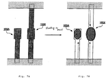
- Fig. 6 is an enlarged view of an area B of the mounting substrate shown in Fig. 3, which shows a state in which the connection pad 103A and the connection pad 103B are placed adjacent to each other.
- like reference numerals will be given to those that have been described before, so that the description thereof will be omitted.
- connection pad 103A which is exposed from the solder resist layer and a portion of the connection pad 103B which is exposed from the solder resist layer have the same shapes, and the portions which are exposed from the solder resist layers are configured so as to have the same areas.
- the connection pad 103B has a pad area 103a having a width W1 and a pad area 103b having a width W2.
- the pad areas 103a are formed so as to have the same lengths La
- the pad areas 103b are formed so as to have the same lengths Lb.
- connection pad 103A and the connection pad 103B are identical to each other in the area of the portion which is exposed from the solder resist layer, as well as the area where the metallic layer 103S is formed. Consequently, scattering of formations (volume, shape) of connecting portions which are used when connected with the semiconductor chip over the plurality of connection pads 103 is decreased, thereby making it possible for the semiconductor chip to be mounted on the mounting substrate with improved reliability.
- connection pads In the event that there exists a difference in exposed area between the connection pads, there is produced variability of formation of connecting portions, and therefore, there may occur a case where the reliability in connecting the semiconductor chip to the mounting substrate is decreased.
- Figs. 7A, (B) are drawings which exemplarily show a problem with a case where connecting portions each made of a solder are formed on connection pads whose exposed areas differ.
- Fig. 7A is a drawing which shows a state in which metallic surfaces are formed on the electrode pad 103A and an electrode pad 103x whose exposed area differs from that of the electrode pad 103A, respectively.
- connecting portions which are formed on the respective connection pads differ in resulting size from each other as is shown in Fig. 7B. Because of this, when the semiconductor chip (Au bumps) is connected, scattering of sizes of connecting portions occurs over the plurality of connection pads, whereby there may occur a case where the reliability in mounting the semiconductor chip on the mounting substrate is decreased.
- connection pad 103A and the connection pad 103B are formed such that the exposed areas thereof are the same, scattering of shapes of connecting portions which are used when connecting the semiconductor chip to the mounting substrate is suppressed, thereby making it possible for the semiconductor chip to be mounted on the mounting substrate.
- the mounting substrate 100 according to the invention the high-performance semiconductor chip in which the connecting portions are placed at narrower intervals can be mounted thereon, and the reliability of the connecting portions of the semiconductor chip is improved.
- connection pads 103A are formed in the vicinity of the corner portions of the solder resist layer 102B and the connection pads 103B are arranged between the connection pads 103A (or between portions in the vicinity of the corner portions), the invention is not limited thereto.
- Fig. 8 is a drawing showing a modified example made to the mounting substrate 100 shown in Fig. 3.
- like reference numerals will be given to those that have been described before, so that the description thereof will be omitted.
- the connection pads 103A and the connection pads 103B can be disposed variously as required.
- the arrangement of the connection pads 103A and the connection pads 103B can be modified variously according to, for example, the specification of the semiconductor chip and the layout of wirings on the mounting substrate.
- an etch stop layer 112 made up of a plated layer of Ni or Sn is formed on a supporting substrate 111 made of, for example, Cu.
- a resist layer is formed on the etch stop layer 112 by laminating a dry film resist thereon, and the resist layer is patterned using a photolithography method, so as to form a resist pattern 113 which has openings 113A therein.
- connection pads 103B made of Cu are formed on the etch stop layers 112 in the openings 113A by, for example, a plating method.
- connection pads 103A are also formed at the same time as the formation of the connection pads 103B.
- an insulation layer 101 made of a so-called build up resin such as an epoxy resin or a polyimide resin is formed in such a manner as to cover the connection pads 103B through laminating.
- via holes 101A are formed in the insulation layer 101 in such a manner as to reach the connection pads 103B by the use of, for example, a YAG laser.
- via plugs 108A which are connected to the connection pads 103B are formed on inner walls of the via holes 101, and patterned wirings 108B which are connected to the via plugs 108A are formed on the insulation layer 111, so as to form the wiring portions 108.
- the supporting substrate 111 and the etch stop layer 112 are removed by etching so as to realize a state in which the connection pads 103B are exposed.
- a solder resist layer 102 having openings 104 is formed in such a manner as to cover end portions o the connection pads 103B.
- the connection pads 103B are made to be exposed from the openings 104.
- solder resist 109 having openings 107A is formed in such a manner as to cover the wiring portions 108.
- the patterned wirings 108B are made to be exposed partially from the openings 107A.
- metallic layers 103S each made of, for example, a solder are formed on surfaces of the connection pads 103B which are exposed from the solder resist layer 102.
- metallic layers 110 each made of, for example, a solder is formed on surfaces of the patterned wirings 108B which are exposed from the solder resist layer 107.
- the mounting substrate 100 shown in Fig. 3 can be fabricated.
- FIG. 10 is a drawing which shows a mounting substrate 200 according to a second embodiment of the invention.
- the mounting substrate 200 is regarded as the same as the mounting substrate 100 unless described otherwise.
- openings 102b are formed in the solder resist layer 102.
- connection pads 103C are formed on the insulation layer 101 in such a manner as to be exposed from the openings 102b.
- the connection pads 103C are formed in such a manner as to be covered by the solder resist layer 102B at end portions thereof.
- the mounting substrate 200 has the construction that has been described above, for example, a semiconductor chip having connecting portions formed at a central portion thereof can be mounted thereon.
- the connection pads 103C are connected to a power supply line or a grounding line of the semiconductor chip which is mounted on the mounting substrate 200.
- the lines of the power supply system are preferably formed in the vicinity of a central portion of a semiconductor chip where devices of the semiconductor chip are formed. Because of this, in semiconductor chips which are designed to cope with the low voltage operation, in order to strengthen the lines for the power supply system, there may be adopted a configuration in which lines for the power supply system are provided additionally in the vicinity of the center of the semiconductor chip.
- a semiconductor chip like this which can deal with the low voltage can be mounted on the mounting substrate according to the embodiment.
- connection pad 103C is preferably formed so as to be the same as the exposed area of the connection pad 103A and the exposed area of the connection pad 103B. As this occurs, scattering of shapes of connecting portions which are used when the semiconductor chip is connected to the mounting substrate can be suppressed, thereby making it possible to mount the semiconductor chip on the mounting substrate with improved reliability.
- the mounting substrate can be provided which can deal with the trend of narrowing intervals at which connecting portions are placed on the semiconductor chip which is mounted thereon.
Abstract
Description
- This application claims priority to
Japanese Patent Application No. 2006-122114, filed April 26, 2006 - The present disclosure generally relates to substrates. In particular, it relates to substrates for mounting a semiconductor chip and to mounting of semiconductor chips on substrates. The present disclosure relates to a mounting substrate on which a semiconductor chip is mounted using a flip chip bonding. Specifically, it relates to a mounting substrate.
- Although there have been proposed various methods of mounting a semiconductor chip on a mounting substrate, for example, a method of mounting a semiconductor chip on a mounting substrate using the flip chip bonding is characteristic in that a package can easily be made small in size and thin in thickness.
- Fig. 1 is a plan view showing an example of a configuration of a mounting substrate on which a semiconductor chip is mounted using the flip chip bonding.
- Referring to Fig. 1, in a mounting substrate 10,
connection pads 13 are formed on aninsulation layer 11 for connection to a semiconductor chip. Asolder resist layer 12 having aopening 14 through which theconnection pads 13 are exposed is formed on theinsulation layer 11. Thesolder resist layer 12 is made up ofsolder resist layers opening 14. In this case, ends of theconnection pads 13 are constructed to be covered by thesolder resist layers - A semiconductor chip 15 (as a matter of convenience in drawing, only briefly indicated by dotted lines for the sake of easy identification), which is to be mounted on the mounting substrate 10, is mounted thereon so that connecting portions (not shown) such as solder bumps which are formed on electrodes of the
semiconductor chip 15 are brought into electrical connection with theconnection pads 13. - In addition, a resin referred to as an underfill is infiltrated between the
semiconductor chip 15 and the mounting substrate 10, so as to realize an insulation between the adjacent connecting portions (connection pads). (See, e.g.,Japanese Patent Unexamined Publication No. 2000-77471 - In recent semiconductor chips, however, intervals at which connecting portions are placed are narrowed so as to increase the number of connecting portions to be placed, and thus, the trend of so-called narrow interval arrangement (or multiple-pin arrangement) has been progressing. When a semiconductor chip like this is attempted to be mounted on a mounting substrate using the flip chip bonding, there has existed a case where the mounting of the semiconductor chip becomes difficult with the related-art mounting substrate.
- Fig. 2 is an enlarged view of a portion lying in the vicinity of a corner portion of the mounting substrate 10 shown in Fig. 1. Note that, however, like reference numerals will be given to those that have already been described before, so that the description thereof will be omitted. As the number of pins to be placed increases, the intervals at which the
connection pads 13 are placed become narrower in association therewith, and furthermore, theconnection pads 13 have to also be formed even in areas closer to the corner portions of the mounting substrate 10. As this occurs, as is shown in Fig. 2, the connection pads come to interfere with each other in the corner portion of the mounting substrate 10, leading to a problem that the placement of the connection pads becomes difficult, in particular, in the corner portions. - In light of the above, the mounting substrate according to independent claim 1 is provided.
Further advantages, features, aspects and details of the invention are evident from the dependent claims, the description and the drawings.
Embodiments of the present invention provide a mounting substrate. - More specifically, embodiments of the present invention provide a mounting substrate which can deal with the trend of narrowing the intervals at which the connecting portions are placed on the semiconductor chip which is mounted on the mounting substrate.
- According to an aspect of one or more embodiments of the invention, a mounting substrate on which a semiconductor chip is mounted using a flip chip bonding, comprises a plurality of connection pads to be connected to the semiconductor chip, and an insulation layer formed in such a manner as to cover the connection pads partially, wherein the insulation layer includes a first insulation layer which is formed in such a manner as to correspond to a center of the semiconductor chip and a second insulation layer which is formed in such a manner as to surround the first insulation layer, and wherein the plurality of connection pads include first connection pads which are partially covered by the first insulation layer and second connection pads which are partially covered by the second insulation layer.
- According to one or more embodiments of the invention, it becomes possible to provide the mounting substrate which can deal with the trend of narrowing the intervals at which the connecting portions are placed on the semiconductor chip which is mounted on the mounting substrate.
- In addition, the insulation layer may be made up of a solder resist layer.
- Additionally, the first insulation layer may be formed into a quadrangle, and the second connection pads may be placed in the vicinity of corner portions of the quadrangle, whereby the mutual interference of the connection pads in the vicinity of the corner portions can be suppressed effectively.
- In addition, in the event that an exposed area of the first connection pad and an exposed area of the second connection pad are the same, the reliability in connection between the connection pads and the semiconductor chip can be improved.
- Additionally, in the event that the mounting substrate further has third connection pads which are exposed from an opening formed in the first insulation layer, a semiconductor chip having connection pads at its central portion can be mounted.
- In addition, in the event that an exposed area of the third connection pad is the same as the exposed area of the first connection pad and the exposed area of the second connection pad, the reliability in connecting the semiconductor chip to the mounting substrate can be improved.
- One or more embodiments of the present invention may include one or more the following advantages. For example, it becomes possible to provide the mounting substrate which can deal with the trend of narrowing the intervals at which the connecting portions are placed on the semiconductor chip which is mounted on the mounting substrate.
- The mounting substrate has both the first connection pads which are partially covered by the first insulation layer and the second connection pads which are partially covered by the second insulation layer. Because of this, the first connection pads or the second connection pads can be disposed in such a manner as to be connected to the connecting portions of the semiconductor chip which are placed at narrower intervals.
- For example, the second connection pads are disposed in the vicinity of the corner portions of the first insulation layer formed which is formed substantially into the quadrangle so as to match the semiconductor chip which is also formed substantially into a quadrangle as viewed from the top thereof, thereby making it possible to avoid the interference of the connection pads. In addition, since both the first connection pads and the second connection pads are formed, there is provided an advantage that the degree of freedom in laying out a connection path using the connection pads is increased.
Embodiments according to the invention are also directed to methods by which the described apparatus is manufactured. It may include method steps for manufacturing parts of the apparatus. The method steps may be performed by way of hardware components, firmware, a computer programmed by appropriate software, by any combination thereof or in any other manner.
Other features and advantages may be apparent from the following detailed description, the accompanying drawings and the claims.
The invention will be better understood by reference to the following description of embodiments of the invention taken in conjunction with the accompanying drawings, wherein: - Fig. 1 is a drawing which shows a related-art mounting substrate.
- Fig. 2 is a drawing which shows a problem inherent in the related-art mounting substrate.
- Fig. 3 is a drawing which shows a mounting substrate according to a first embodiment.
- Fig. 4 is a (first) drawing which shows connection pads of the mounting substrate of the first embodiment.
- Figs. 5A, 5B are drawings which show a method for forming solder connecting portions on the connection pads shown in Fig. 4.
- Fig. 6 is a (second) drawing which shows the connection pads of the mounting substrate shown in Fig. 3.
- Figs. 7A, 7B are drawings which show a problem inherent in related-art connection pads.
- Fig. 8 is a drawing which shows a modified example made to the mounting substrate shown in Fig. 3.
- Fig. 9A is a (first) drawing which shows a fabricating method of the mounting substrate shown in Fig. 3.
- Fig. 9B is a (second) drawing which shows the fabricating method of the mounting substrate shown in Fig. 3.
- Fig. 9C is a (third) drawing which shows the fabricating method of the mounting substrate shown in Fig. 3.
- Fig. 9D is a (fourth) drawing which shows the fabricating method of the mounting substrate shown in Fig. 3.
- Fig. 9E is a (fifth) drawing which shows the fabricating method of the mounting substrate shown in Fig. 3.
- Fig. 9F is a (sixth) drawing which shows the fabricating method of the mounting substrate shown in Fig. 3.
- Fig. 9G is a (seventh) drawing which shows the fabricating method of the mounting substrate shown in Fig. 3.
- Fig. 9H is an (eighth) drawing which shows the fabricating method of the mounting substrate shown in Fig. 3.
- Fig. 9I is a (ninth) drawing which shows the fabricating method of the mounting substrate shown in Fig. 3.
- Fig. 10 is a drawing which shows a mounting substrate according to a second embodiment.
- Next, embodiments of the mounting substrate will be described based on the accompanying drawings.
- Fig. 3 is a plan view showing exemplarily a mounting substrate 100 according to a first embodiment of the invention. Referring to Fig. 3, the mounting substrate 100 shown in the figure has a construction in which
connection pads 103 adapted to be connected to a semiconductor chip are formed on aninsulation layer 101. Theconnection pads 103 are covered partially by an insulation layer (a solder resist layer) 102 which is formed on theinsulation layer 101. - The solder resist layer is formed into a solder resist
layer 102A and a solder resistlayer 102B which are separated from each other across an opening 140. The solder resistlayer 102B is formed so as to mach the shape of the semiconductor chip and is formed into, for example, a quadrangular shape as viewed from the top thereof. On the other hand, the solder resistlayer 102A is formed so as to surround the solder resistlayer 102B. - The
connection pads 103 are formed on theinsulation layer 101 in such a manner as to be partially exposed from theopening 104. Theconnection pads 103 are configured so as to includeconnection pads 103A which are covered by the solder resistlayer 102A at end portions thereof andconnection pads 103B which are covered by the solder resistlayer 102B at end portions thereof. - Namely, in the mounting substrate 100 of this embodiment, the connection pads which are connected to the semiconductor chip are configured so as to include the
connection pads 103B which are covered by the solder resistlayer 102B which is formed at a central portion of the mounting substrate and theconnection pads 103A which are covered by the solder resistlayer 102A which is formed at a circumferential edge portion of the mounting substrate. - Because of this, in the mounting substrate, the
connection pads 103A and theconnection pads 103B can be disposed at narrow intervals while avoiding the interference therebetween. Consequently, the semiconductor chip in which the connecting portions are placed at narrower intervals (that is, more pins are placed) can easily be mounted on the mounting substrate. - For example, the
connection pads 103A which are covered by the solder resistlayer 102A at the end portions (or whose end portions are extended towards a circumferential edge portion of the mounting substrate) are placed in the vicinity of corner portions of the mounting substrate 100 (or in the vicinity of corner portions of the solder resistlayer 102B). In this case, theconnection pads 103A are formed in such a manner as not to be brought into contact with the solder resistlayer 102B. - Because of this, in the vicinity of the corner portions, the plurality of
connection pads 103A can be placed without any interference therebetween. Because of this, it is seen that the mounting substrate 100 is constructed such that the semiconductor chip in which the connecting portions are placed at narrower intervals can easily be mounted thereon. - Fig. 4 is an enlarged view which shows a state in which the
connection pad 103A is placed. In the description of theconnection pad 103A, like reference numerals will be given to those that have been described before, so that the description thereof will be omitted therein. Referring to Fig. 4, theconnection pad 103A which is covered by the solder resistlayer 102A at the end portion thereof has a construction in which apad area 103a and apad area 103b are connected together to form theconnection pad 103A. In addition, a width W1 of thepad area 103a is configured so as to become wider than a width W2 of thepad area 103b. - Since it has the construction described above, the
connection pad 103A provides an advantage that the electrical connection thereof with the connecting portion (for example, a Au bump) on the semiconductor chip can be facilitated. The reason therefor will be described based on a forming method of a connecting portion with the semiconductor chip shown in Figs. 5A, 5B. In the description of the forming method, like reference numerals will be given to those that have been described before, so that the description thereof will be omitted. - Firstly, in a state shown in Fig. 5A, a
metallic layer 103S having a low melt point which is made of, for example, a solder is formed on theconnection pad 103A (thepad areas metallic layer 103S is formed of, for example, minute solder powder or by virtue of metal plating of a solder, the invention is not limited to such methods. - Next, in a state shown in Fig. 5B, the
connection pad 103A (the mounting substrate) is heated so as to melt themetallic layer 103S. At this point in time, the solder so melted is gathered from thepad area 103b whose width W2 is narrower to thepad area 103a whose width W1 is wider by virtue of surface tension, so as to form a connecting portion 103PB made of solder. For example, a connecting portion (a Au bump or the like) of the semiconductor chip which is placed at, for example, thepad area 103a is electrically connected to theconnection pad 103A by the connecting portion 103BP. - In the mounting substrate according to this embodiment, since the connecting portion is formed by virtue of the surface tension of the metal which is melt as described above, the area of the connection pad (an area where a metallic layer formed by the melted metal) is preferably the same between a plurality of connection pads.
- Fig. 6 is an enlarged view of an area B of the mounting substrate shown in Fig. 3, which shows a state in which the
connection pad 103A and theconnection pad 103B are placed adjacent to each other. In the description of the state, like reference numerals will be given to those that have been described before, so that the description thereof will be omitted. - Referring to Fig. 6, in the mounting substrate 100 of this embodiment, a portion of the
connection pad 103A which is exposed from the solder resist layer and a portion of theconnection pad 103B which is exposed from the solder resist layer have the same shapes, and the portions which are exposed from the solder resist layers are configured so as to have the same areas. For example, as with theconnection pad area 103A, theconnection pad 103B has apad area 103a having a width W1 and apad area 103b having a width W2. In addition, in theconnection pad 103A and theconnection pad 103B, thepad areas 103a are formed so as to have the same lengths La, and thepad areas 103b are formed so as to have the same lengths Lb. - Because of this, the
connection pad 103A and theconnection pad 103B are identical to each other in the area of the portion which is exposed from the solder resist layer, as well as the area where themetallic layer 103S is formed. Consequently, scattering of formations (volume, shape) of connecting portions which are used when connected with the semiconductor chip over the plurality ofconnection pads 103 is decreased, thereby making it possible for the semiconductor chip to be mounted on the mounting substrate with improved reliability. - For example, in the event that there exists a difference in exposed area between the connection pads, there is produced variability of formation of connecting portions, and therefore, there may occur a case where the reliability in connecting the semiconductor chip to the mounting substrate is decreased.
- Figs. 7A, (B) are drawings which exemplarily show a problem with a case where connecting portions each made of a solder are formed on connection pads whose exposed areas differ.
- Firstly, Fig. 7A is a drawing which shows a state in which metallic surfaces are formed on the
electrode pad 103A and an electrode pad 103x whose exposed area differs from that of theelectrode pad 103A, respectively. Here, when the respective connection pads are heated for the metallic layers thereon to melt, connecting portions which are formed on the respective connection pads differ in resulting size from each other as is shown in Fig. 7B. Because of this, when the semiconductor chip (Au bumps) is connected, scattering of sizes of connecting portions occurs over the plurality of connection pads, whereby there may occur a case where the reliability in mounting the semiconductor chip on the mounting substrate is decreased. - For example, in the related-art mounting substrate shown in Fig. 1, in the event that a construction is adopted in which only the portions are deleted where the connection pads interfere with each other, the areas where the connection pads are exposed differ as is shown in Fig. 7, causing concern that the reliability in connecting the semiconductor chip to the mounting substrate is decreased.
- On the other hand, with the mounting substrate according to this embodiment, since the
connection pad 103A and theconnection pad 103B are formed such that the exposed areas thereof are the same, scattering of shapes of connecting portions which are used when connecting the semiconductor chip to the mounting substrate is suppressed, thereby making it possible for the semiconductor chip to be mounted on the mounting substrate. - Namely, with the mounting substrate 100 according to the invention, the high-performance semiconductor chip in which the connecting portions are placed at narrower intervals can be mounted thereon, and the reliability of the connecting portions of the semiconductor chip is improved.
- In addition, while in the embodiment, the
connection pads 103A are formed in the vicinity of the corner portions of the solder resistlayer 102B and theconnection pads 103B are arranged between theconnection pads 103A (or between portions in the vicinity of the corner portions), the invention is not limited thereto. - Fig. 8 is a drawing showing a modified example made to the mounting substrate 100 shown in Fig. 3. In the description of the modified example, like reference numerals will be given to those that have been described before, so that the description thereof will be omitted. As is shown in Fig. 8, the
connection pads 103A and theconnection pads 103B can be disposed variously as required. For example, the arrangement of theconnection pads 103A and theconnection pads 103B can be modified variously according to, for example, the specification of the semiconductor chip and the layout of wirings on the mounting substrate. - Next, an example of a fabricating method of the mounting substrate 100 will be described based on Figs. 9A to 9I. In the description of the method, like reference numerals will be given to the portions which have been described before, so that the description thereof will be omitted.
- Firstly, in a step shown in Fig. 9A, an
etch stop layer 112 made up of a plated layer of Ni or Sn is formed on a supportingsubstrate 111 made of, for example, Cu. - Next, in a step shown in Fig. 9B, a resist layer is formed on the
etch stop layer 112 by laminating a dry film resist thereon, and the resist layer is patterned using a photolithography method, so as to form a resistpattern 113 which hasopenings 113A therein. - Next, in a step shown in Fig. 9C,
connection pads 103B made of Cu are formed on the etch stop layers 112 in theopenings 113A by, for example, a plating method. In this case, although not shown,connection pads 103A are also formed at the same time as the formation of theconnection pads 103B. - Next, in a step shown in Fig. 9D, after the resist
pattern 113 is removed from the supportingsubstrate 111, aninsulation layer 101 made of a so-called build up resin such as an epoxy resin or a polyimide resin is formed in such a manner as to cover theconnection pads 103B through laminating. - Next, in a step shown in Fig. 9E, via
holes 101A are formed in theinsulation layer 101 in such a manner as to reach theconnection pads 103B by the use of, for example, a YAG laser. - Next, in a step shown in Fig. 9F, by the use of the plating method using Cu, via
plugs 108A which are connected to theconnection pads 103B are formed on inner walls of the via holes 101, andpatterned wirings 108B which are connected to the via plugs 108A are formed on theinsulation layer 111, so as to form thewiring portions 108. - Next, in a step shown in Fig. 9G, the supporting
substrate 111 and theetch stop layer 112 are removed by etching so as to realize a state in which theconnection pads 103B are exposed. - Next, in a step shown in Fig. 9H, a solder resist
layer 102 havingopenings 104 is formed in such a manner as to cover end portions o theconnection pads 103B. In addition, theconnection pads 103B are made to be exposed from theopenings 104. - Similarly, a solder resist 109 having
openings 107A is formed in such a manner as to cover thewiring portions 108. In addition, the patternedwirings 108B are made to be exposed partially from theopenings 107A. - Next, in a step shown in Fig. 9I,
metallic layers 103S each made of, for example, a solder are formed on surfaces of theconnection pads 103B which are exposed from the solder resistlayer 102. Similarly,metallic layers 110 each made of, for example, a solder is formed on surfaces of the patternedwirings 108B which are exposed from the solder resist layer 107. - Thus, the mounting substrate 100 shown in Fig. 3 can be fabricated.
- In addition, Fig. 10 is a drawing which shows a mounting substrate 200 according to a second embodiment of the invention. In the description of this second embodiment, like reference numerals will be given to those that have been described before, so that the description thereof will be omitted. In addition, the mounting substrate 200 is regarded as the same as the mounting substrate 100 unless described otherwise.
- Referring to Fig. 10, in the mounting substrate 200 according to this embodiment,
openings 102b are formed in the solder resistlayer 102. In addition,connection pads 103C are formed on theinsulation layer 101 in such a manner as to be exposed from theopenings 102b. As with theconnection pads 103B, theconnection pads 103C are formed in such a manner as to be covered by the solder resistlayer 102B at end portions thereof. - Since the mounting substrate 200 according to this embodiment has the construction that has been described above, for example, a semiconductor chip having connecting portions formed at a central portion thereof can be mounted thereon. For example, the
connection pads 103C are connected to a power supply line or a grounding line of the semiconductor chip which is mounted on the mounting substrate 200. In recent years, there is a strong demand, in particular, for semiconductor chips which consumes less electric power (or semiconductor chips which operates at a low voltage), and to deal with the trend of low voltage operation, the lines of the power supply system are preferably formed in the vicinity of a central portion of a semiconductor chip where devices of the semiconductor chip are formed. Because of this, in semiconductor chips which are designed to cope with the low voltage operation, in order to strengthen the lines for the power supply system, there may be adopted a configuration in which lines for the power supply system are provided additionally in the vicinity of the center of the semiconductor chip. - A semiconductor chip like this which can deal with the low voltage can be mounted on the mounting substrate according to the embodiment.
- In addition, in the construction that has been described above, an exposed area of the
connection pad 103C is preferably formed so as to be the same as the exposed area of theconnection pad 103A and the exposed area of theconnection pad 103B. As this occurs, scattering of shapes of connecting portions which are used when the semiconductor chip is connected to the mounting substrate can be suppressed, thereby making it possible to mount the semiconductor chip on the mounting substrate with improved reliability. - Thus, while the invention has been described based on the preferred embodiments, the invention is not limited to those specific embodiments that have been described heretofore but can be modified and/or changed variously without departing from the spirit and scope of the invention which are described under the claims of the invention.
- According to the invention, the mounting substrate can be provided which can deal with the trend of narrowing intervals at which connecting portions are placed on the semiconductor chip which is mounted thereon.
Claims (6)
- A mounting substrate on which a semiconductor chip is mounted using a flip chip bonding, comprising:a plurality of connection pads (103) to be connected to the semiconductor chip; andan insulation layer (102) formed in such a manner as to cover the connection pads partially,wherein the insulation layer includes a first insulation layer (102B) which is formed in such a manner as to correspond to a center of the semiconductor chip and a second insulation layer (102A) which is formed in such a manner as to surround the first insulation layer, and
wherein the plurality of connection pads (103) include first connection pads (103B) which are partially covered by the first insulation layer and second connection pads (103A) which are partially covered by the second insulation layer. - The mounting substrate as set forth in Claim 1, wherein the insulation layer (102) is made up of a solder resist layer.
- The mounting substrate as set forth in Claim 1 or 2, wherein the first insulation layer is formed into a quadrangle, and the second connection pads are placed in the vicinity of corner portions of the quadrangle.
- The mounting substrate as set forth in any of Claims 1 to 3, wherein an exposed area of the first connection pad and an exposed area of the second connection pad are the same.
- The mounting substrate as set forth in any of Claims 1 to 4, wherein the plurality of connection pads (103) further include third connection pads (103C) which are exposed from an opening formed in the first insulation layer (102B).
- The mounting substrate as set forth in Claim 5, wherein an exposed area of the third connection pad is the same as the exposed area of the first connection pad and the exposed area of the second connection pad.
Applications Claiming Priority (1)
| Application Number | Priority Date | Filing Date | Title |
|---|---|---|---|
| JP2006122114A JP4758813B2 (en) | 2006-04-26 | 2006-04-26 | Mounting board |
Publications (2)
| Publication Number | Publication Date |
|---|---|
| EP1850381A2 true EP1850381A2 (en) | 2007-10-31 |
| EP1850381A3 EP1850381A3 (en) | 2010-08-18 |
Family
ID=38344758
Family Applications (1)
| Application Number | Title | Priority Date | Filing Date |
|---|---|---|---|
| EP07008530A Withdrawn EP1850381A3 (en) | 2006-04-26 | 2007-04-26 | Mounting substrate |
Country Status (5)
| Country | Link |
|---|---|
| US (1) | US7598608B2 (en) |
| EP (1) | EP1850381A3 (en) |
| JP (1) | JP4758813B2 (en) |
| KR (1) | KR20070105853A (en) |
| TW (1) | TW200807662A (en) |
Families Citing this family (6)
| Publication number | Priority date | Publication date | Assignee | Title |
|---|---|---|---|---|
| KR101005242B1 (en) * | 2008-03-03 | 2011-01-04 | 삼성전기주식회사 | Heat radiating printed circuit board and semiconductor chip package |
| US8653375B2 (en) | 2008-08-21 | 2014-02-18 | Agere Systems, Inc. | Mitigation of whiskers in Sn-films |
| US8536718B2 (en) * | 2010-06-24 | 2013-09-17 | Stats Chippac Ltd. | Integrated circuit packaging system with trenches and method of manufacture thereof |
| US8766461B1 (en) * | 2013-01-16 | 2014-07-01 | Texas Instruments Incorporated | Substrate with bond fingers |
| JP6251828B2 (en) * | 2017-01-30 | 2017-12-20 | ルネサスエレクトロニクス株式会社 | Semiconductor device |
| JP7072644B2 (en) * | 2018-04-26 | 2022-05-20 | 京セラ株式会社 | Electronic element mounting boards, electronic devices, and electronic modules |
Citations (2)
| Publication number | Priority date | Publication date | Assignee | Title |
|---|---|---|---|---|
| US20050103516A1 (en) * | 2003-09-30 | 2005-05-19 | Tdk Corporation | Flip-chip mounting circuit board, manufacturing method thereof and integrated circuit device |
| US20060033210A1 (en) * | 2004-08-12 | 2006-02-16 | Texas Instruments Incorporated | Fine pitch low-cost flip chip substrate |
Family Cites Families (5)
| Publication number | Priority date | Publication date | Assignee | Title |
|---|---|---|---|---|
| US20040061220A1 (en) * | 1996-03-22 | 2004-04-01 | Chuichi Miyazaki | Semiconductor device and manufacturing method thereof |
| JP3420076B2 (en) | 1998-08-31 | 2003-06-23 | 新光電気工業株式会社 | Method for manufacturing flip-chip mounting board, flip-chip mounting board, and flip-chip mounting structure |
| JP4177950B2 (en) * | 2000-03-28 | 2008-11-05 | ローム株式会社 | Manufacturing method of semiconductor device |
| JP3914094B2 (en) * | 2002-06-04 | 2007-05-16 | 松下電器産業株式会社 | Semiconductor device |
| TWI240389B (en) * | 2004-05-06 | 2005-09-21 | Advanced Semiconductor Eng | High-density layout substrate for flip-chip package |
-
2006
- 2006-04-26 JP JP2006122114A patent/JP4758813B2/en not_active Expired - Fee Related
-
2007
- 2007-04-18 US US11/736,916 patent/US7598608B2/en not_active Expired - Fee Related
- 2007-04-18 KR KR1020070037742A patent/KR20070105853A/en not_active Application Discontinuation
- 2007-04-23 TW TW096114223A patent/TW200807662A/en unknown
- 2007-04-26 EP EP07008530A patent/EP1850381A3/en not_active Withdrawn
Patent Citations (2)
| Publication number | Priority date | Publication date | Assignee | Title |
|---|---|---|---|---|
| US20050103516A1 (en) * | 2003-09-30 | 2005-05-19 | Tdk Corporation | Flip-chip mounting circuit board, manufacturing method thereof and integrated circuit device |
| US20060033210A1 (en) * | 2004-08-12 | 2006-02-16 | Texas Instruments Incorporated | Fine pitch low-cost flip chip substrate |
Also Published As
| Publication number | Publication date |
|---|---|
| US7598608B2 (en) | 2009-10-06 |
| US20070252286A1 (en) | 2007-11-01 |
| KR20070105853A (en) | 2007-10-31 |
| JP2007294735A (en) | 2007-11-08 |
| JP4758813B2 (en) | 2011-08-31 |
| EP1850381A3 (en) | 2010-08-18 |
| TW200807662A (en) | 2008-02-01 |
Similar Documents
| Publication | Publication Date | Title |
|---|---|---|
| US7563645B2 (en) | Electronic package having a folded package substrate | |
| US8115300B2 (en) | Wiring substrate and manufacturing method thereof, and semiconductor apparatus | |
| US20060038235A1 (en) | Semiconductor device | |
| US10573614B2 (en) | Process for fabricating a circuit substrate | |
| EP1850381A2 (en) | Mounting substrate | |
| JP2001127198A (en) | Surface-mount board and structure | |
| JP3927783B2 (en) | Semiconductor parts | |
| WO2006112337A1 (en) | Semiconductor device and semiconductor device manufacturing method | |
| US20130258623A1 (en) | Package structure having embedded electronic element and fabrication method thereof | |
| KR101477818B1 (en) | Printed circuit board and method of manufacturing the same | |
| US20190254164A1 (en) | Circuit board, method of manufacturing circuit board, and electronic device | |
| JP6109078B2 (en) | Electronic device tape with enhanced lead cracks | |
| CN102270619A (en) | Pad configurations for an electronic package assembly | |
| JP2005252227A (en) | Film substrate, and the manufacturing method and image display substrate | |
| EP1041618A1 (en) | Semiconductor device and manufacturing method thereof, circuit board and electronic equipment | |
| US20100112757A1 (en) | Electronic device package and method of manufacturing the same | |
| JP6674284B2 (en) | Mounting structure and module | |
| JP2008078646A (en) | Printed circuit board for package, and manufacturing method thereof | |
| JP2004112143A (en) | Connecting structure of conductor for high frequency signal and semiconductor integrated circuit package | |
| US20030159282A1 (en) | Wiring board and method of fabricating the same, semiconductor device, and electronic instrument | |
| JP2011040575A (en) | Electronic device, and method of manufacturing the same | |
| JP3692810B2 (en) | Semiconductor device and manufacturing method thereof, circuit board, and electronic apparatus | |
| KR20100123941A (en) | Substrate for manufacturing semiconductor package and semiconductor package using it | |
| JP2008060404A (en) | Flexible wiring board and manufacturing method of the flexible wiring board | |
| JP2008124107A (en) | Wiring board, semiconductor part and manufacturing method for wiring board |
Legal Events
| Date | Code | Title | Description |
|---|---|---|---|
| PUAI | Public reference made under article 153(3) epc to a published international application that has entered the european phase |
Free format text: ORIGINAL CODE: 0009012 |
|
| AK | Designated contracting states |
Kind code of ref document: A2 Designated state(s): AT BE BG CH CY CZ DE DK EE ES FI FR GB GR HU IE IS IT LI LT LU LV MC MT NL PL PT RO SE SI SK TR |
|
| AX | Request for extension of the european patent |
Extension state: AL BA HR MK YU |
|
| PUAL | Search report despatched |
Free format text: ORIGINAL CODE: 0009013 |
|
| AK | Designated contracting states |
Kind code of ref document: A3 Designated state(s): AT BE BG CH CY CZ DE DK EE ES FI FR GB GR HU IE IS IT LI LT LU LV MC MT NL PL PT RO SE SI SK TR |
|
| AX | Request for extension of the european patent |
Extension state: AL BA HR MK RS |
|
| RIC1 | Information provided on ipc code assigned before grant |
Ipc: H01L 23/498 20060101ALI20100715BHEP Ipc: H05K 1/11 20060101ALI20100715BHEP Ipc: H01L 23/485 20060101AFI20070820BHEP |
|
| AKY | No designation fees paid | ||
| STAA | Information on the status of an ep patent application or granted ep patent |
Free format text: STATUS: THE APPLICATION IS DEEMED TO BE WITHDRAWN |
|
| 18D | Application deemed to be withdrawn |
Effective date: 20110219 |