EP1848592B1 - Printhead module - Google Patents
Printhead module Download PDFInfo
- Publication number
- EP1848592B1 EP1848592B1 EP05854400A EP05854400A EP1848592B1 EP 1848592 B1 EP1848592 B1 EP 1848592B1 EP 05854400 A EP05854400 A EP 05854400A EP 05854400 A EP05854400 A EP 05854400A EP 1848592 B1 EP1848592 B1 EP 1848592B1
- Authority
- EP
- European Patent Office
- Prior art keywords
- printhead
- nozzle
- printing liquid
- ink
- pumping chamber
- Prior art date
- Legal status (The legal status is an assumption and is not a legal conclusion. Google has not performed a legal analysis and makes no representation as to the accuracy of the status listed.)
- Active
Links
- 239000007788 liquid Substances 0.000 claims abstract description 48
- 238000005086 pumping Methods 0.000 claims description 86
- 238000007639 printing Methods 0.000 claims description 39
- 238000004891 communication Methods 0.000 claims description 17
- 239000012530 fluid Substances 0.000 claims description 17
- 239000000463 material Substances 0.000 claims description 14
- 239000010410 layer Substances 0.000 description 98
- 239000000758 substrate Substances 0.000 description 40
- XUIMIQQOPSSXEZ-UHFFFAOYSA-N Silicon Chemical compound [Si] XUIMIQQOPSSXEZ-UHFFFAOYSA-N 0.000 description 33
- 229910052710 silicon Inorganic materials 0.000 description 33
- 239000010703 silicon Substances 0.000 description 33
- 238000000034 method Methods 0.000 description 12
- 229920002120 photoresistant polymer Polymers 0.000 description 12
- 238000005530 etching Methods 0.000 description 10
- 229910052751 metal Inorganic materials 0.000 description 10
- 239000002184 metal Substances 0.000 description 10
- 238000004519 manufacturing process Methods 0.000 description 7
- 230000008569 process Effects 0.000 description 7
- 239000004020 conductor Substances 0.000 description 6
- PCHJSUWPFVWCPO-UHFFFAOYSA-N gold Chemical compound [Au] PCHJSUWPFVWCPO-UHFFFAOYSA-N 0.000 description 5
- 239000010931 gold Substances 0.000 description 5
- 229910052737 gold Inorganic materials 0.000 description 5
- 238000001020 plasma etching Methods 0.000 description 4
- 238000009623 Bosch process Methods 0.000 description 3
- 239000002318 adhesion promoter Substances 0.000 description 3
- 238000000708 deep reactive-ion etching Methods 0.000 description 3
- -1 e.g. Substances 0.000 description 3
- 238000009616 inductively coupled plasma Methods 0.000 description 3
- 229910001120 nichrome Inorganic materials 0.000 description 3
- 238000012360 testing method Methods 0.000 description 3
- RILZRCJGXSFXNE-UHFFFAOYSA-N 2-[4-(trifluoromethoxy)phenyl]ethanol Chemical compound OCCC1=CC=C(OC(F)(F)F)C=C1 RILZRCJGXSFXNE-UHFFFAOYSA-N 0.000 description 2
- 241000252506 Characiformes Species 0.000 description 2
- MHAJPDPJQMAIIY-UHFFFAOYSA-N Hydrogen peroxide Chemical compound OO MHAJPDPJQMAIIY-UHFFFAOYSA-N 0.000 description 2
- QAOWNCQODCNURD-UHFFFAOYSA-N Sulfuric acid Chemical compound OS(O)(=O)=O QAOWNCQODCNURD-UHFFFAOYSA-N 0.000 description 2
- 230000009471 action Effects 0.000 description 2
- 239000000853 adhesive Substances 0.000 description 2
- 230000001070 adhesive effect Effects 0.000 description 2
- 238000011109 contamination Methods 0.000 description 2
- 238000000151 deposition Methods 0.000 description 2
- 238000000227 grinding Methods 0.000 description 2
- 238000002955 isolation Methods 0.000 description 2
- 239000012528 membrane Substances 0.000 description 2
- 229920000642 polymer Polymers 0.000 description 2
- 230000037452 priming Effects 0.000 description 2
- 230000003134 recirculating effect Effects 0.000 description 2
- 230000004044 response Effects 0.000 description 2
- 239000004065 semiconductor Substances 0.000 description 2
- VYPSYNLAJGMNEJ-UHFFFAOYSA-N silicon dioxide Inorganic materials O=[Si]=O VYPSYNLAJGMNEJ-UHFFFAOYSA-N 0.000 description 2
- 238000004544 sputter deposition Methods 0.000 description 2
- 229910052721 tungsten Inorganic materials 0.000 description 2
- 239000010937 tungsten Substances 0.000 description 2
- VYZAMTAEIAYCRO-UHFFFAOYSA-N Chromium Chemical compound [Cr] VYZAMTAEIAYCRO-UHFFFAOYSA-N 0.000 description 1
- 229910004039 HBF4 Inorganic materials 0.000 description 1
- 239000012790 adhesive layer Substances 0.000 description 1
- 238000000137 annealing Methods 0.000 description 1
- 230000004888 barrier function Effects 0.000 description 1
- 238000005452 bending Methods 0.000 description 1
- 239000000356 contaminant Substances 0.000 description 1
- 230000000694 effects Effects 0.000 description 1
- 239000003517 fume Substances 0.000 description 1
- 230000004927 fusion Effects 0.000 description 1
- FFUAGWLWBBFQJT-UHFFFAOYSA-N hexamethyldisilazane Chemical compound C[Si](C)(C)N[Si](C)(C)C FFUAGWLWBBFQJT-UHFFFAOYSA-N 0.000 description 1
- 239000012212 insulator Substances 0.000 description 1
- 239000004973 liquid crystal related substance Substances 0.000 description 1
- 229910001338 liquidmetal Inorganic materials 0.000 description 1
- 230000000873 masking effect Effects 0.000 description 1
- 238000012986 modification Methods 0.000 description 1
- 230000004048 modification Effects 0.000 description 1
- 229910021421 monocrystalline silicon Inorganic materials 0.000 description 1
- 238000012545 processing Methods 0.000 description 1
- 230000001681 protective effect Effects 0.000 description 1
- 239000010453 quartz Substances 0.000 description 1
- 229910052814 silicon oxide Inorganic materials 0.000 description 1
- MAKDTFFYCIMFQP-UHFFFAOYSA-N titanium tungsten Chemical compound [Ti].[W] MAKDTFFYCIMFQP-UHFFFAOYSA-N 0.000 description 1
- 238000010792 warming Methods 0.000 description 1
Images


Classifications
-
- B—PERFORMING OPERATIONS; TRANSPORTING
- B41—PRINTING; LINING MACHINES; TYPEWRITERS; STAMPS
- B41J—TYPEWRITERS; SELECTIVE PRINTING MECHANISMS, i.e. MECHANISMS PRINTING OTHERWISE THAN FROM A FORME; CORRECTION OF TYPOGRAPHICAL ERRORS
- B41J2/00—Typewriters or selective printing mechanisms characterised by the printing or marking process for which they are designed
- B41J2/005—Typewriters or selective printing mechanisms characterised by the printing or marking process for which they are designed characterised by bringing liquid or particles selectively into contact with a printing material
- B41J2/01—Ink jet
- B41J2/135—Nozzles
- B41J2/145—Arrangement thereof
-
- B—PERFORMING OPERATIONS; TRANSPORTING
- B41—PRINTING; LINING MACHINES; TYPEWRITERS; STAMPS
- B41J—TYPEWRITERS; SELECTIVE PRINTING MECHANISMS, i.e. MECHANISMS PRINTING OTHERWISE THAN FROM A FORME; CORRECTION OF TYPOGRAPHICAL ERRORS
- B41J2/00—Typewriters or selective printing mechanisms characterised by the printing or marking process for which they are designed
- B41J2/005—Typewriters or selective printing mechanisms characterised by the printing or marking process for which they are designed characterised by bringing liquid or particles selectively into contact with a printing material
- B41J2/01—Ink jet
- B41J2/17—Ink jet characterised by ink handling
-
- B—PERFORMING OPERATIONS; TRANSPORTING
- B41—PRINTING; LINING MACHINES; TYPEWRITERS; STAMPS
- B41J—TYPEWRITERS; SELECTIVE PRINTING MECHANISMS, i.e. MECHANISMS PRINTING OTHERWISE THAN FROM A FORME; CORRECTION OF TYPOGRAPHICAL ERRORS
- B41J2/00—Typewriters or selective printing mechanisms characterised by the printing or marking process for which they are designed
- B41J2/005—Typewriters or selective printing mechanisms characterised by the printing or marking process for which they are designed characterised by bringing liquid or particles selectively into contact with a printing material
- B41J2/01—Ink jet
- B41J2/135—Nozzles
- B41J2/14—Structure thereof only for on-demand ink jet heads
- B41J2/14201—Structure of print heads with piezoelectric elements
- B41J2/14233—Structure of print heads with piezoelectric elements of film type, deformed by bending and disposed on a diaphragm
-
- B—PERFORMING OPERATIONS; TRANSPORTING
- B41—PRINTING; LINING MACHINES; TYPEWRITERS; STAMPS
- B41J—TYPEWRITERS; SELECTIVE PRINTING MECHANISMS, i.e. MECHANISMS PRINTING OTHERWISE THAN FROM A FORME; CORRECTION OF TYPOGRAPHICAL ERRORS
- B41J2/00—Typewriters or selective printing mechanisms characterised by the printing or marking process for which they are designed
- B41J2/005—Typewriters or selective printing mechanisms characterised by the printing or marking process for which they are designed characterised by bringing liquid or particles selectively into contact with a printing material
- B41J2/01—Ink jet
- B41J2/135—Nozzles
- B41J2/16—Production of nozzles
- B41J2/1607—Production of print heads with piezoelectric elements
- B41J2/161—Production of print heads with piezoelectric elements of film type, deformed by bending and disposed on a diaphragm
-
- B—PERFORMING OPERATIONS; TRANSPORTING
- B41—PRINTING; LINING MACHINES; TYPEWRITERS; STAMPS
- B41J—TYPEWRITERS; SELECTIVE PRINTING MECHANISMS, i.e. MECHANISMS PRINTING OTHERWISE THAN FROM A FORME; CORRECTION OF TYPOGRAPHICAL ERRORS
- B41J2/00—Typewriters or selective printing mechanisms characterised by the printing or marking process for which they are designed
- B41J2/005—Typewriters or selective printing mechanisms characterised by the printing or marking process for which they are designed characterised by bringing liquid or particles selectively into contact with a printing material
- B41J2/01—Ink jet
- B41J2/135—Nozzles
- B41J2/16—Production of nozzles
- B41J2/1621—Manufacturing processes
- B41J2/1626—Manufacturing processes etching
- B41J2/1628—Manufacturing processes etching dry etching
-
- B—PERFORMING OPERATIONS; TRANSPORTING
- B41—PRINTING; LINING MACHINES; TYPEWRITERS; STAMPS
- B41J—TYPEWRITERS; SELECTIVE PRINTING MECHANISMS, i.e. MECHANISMS PRINTING OTHERWISE THAN FROM A FORME; CORRECTION OF TYPOGRAPHICAL ERRORS
- B41J2/00—Typewriters or selective printing mechanisms characterised by the printing or marking process for which they are designed
- B41J2/005—Typewriters or selective printing mechanisms characterised by the printing or marking process for which they are designed characterised by bringing liquid or particles selectively into contact with a printing material
- B41J2/01—Ink jet
- B41J2/135—Nozzles
- B41J2/16—Production of nozzles
- B41J2/1621—Manufacturing processes
- B41J2/1626—Manufacturing processes etching
- B41J2/1629—Manufacturing processes etching wet etching
-
- B—PERFORMING OPERATIONS; TRANSPORTING
- B41—PRINTING; LINING MACHINES; TYPEWRITERS; STAMPS
- B41J—TYPEWRITERS; SELECTIVE PRINTING MECHANISMS, i.e. MECHANISMS PRINTING OTHERWISE THAN FROM A FORME; CORRECTION OF TYPOGRAPHICAL ERRORS
- B41J2/00—Typewriters or selective printing mechanisms characterised by the printing or marking process for which they are designed
- B41J2/005—Typewriters or selective printing mechanisms characterised by the printing or marking process for which they are designed characterised by bringing liquid or particles selectively into contact with a printing material
- B41J2/01—Ink jet
- B41J2/135—Nozzles
- B41J2/16—Production of nozzles
- B41J2/1621—Manufacturing processes
- B41J2/1631—Manufacturing processes photolithography
-
- B—PERFORMING OPERATIONS; TRANSPORTING
- B41—PRINTING; LINING MACHINES; TYPEWRITERS; STAMPS
- B41J—TYPEWRITERS; SELECTIVE PRINTING MECHANISMS, i.e. MECHANISMS PRINTING OTHERWISE THAN FROM A FORME; CORRECTION OF TYPOGRAPHICAL ERRORS
- B41J2/00—Typewriters or selective printing mechanisms characterised by the printing or marking process for which they are designed
- B41J2/005—Typewriters or selective printing mechanisms characterised by the printing or marking process for which they are designed characterised by bringing liquid or particles selectively into contact with a printing material
- B41J2/01—Ink jet
- B41J2/135—Nozzles
- B41J2/16—Production of nozzles
- B41J2/1621—Manufacturing processes
- B41J2/1632—Manufacturing processes machining
-
- B—PERFORMING OPERATIONS; TRANSPORTING
- B41—PRINTING; LINING MACHINES; TYPEWRITERS; STAMPS
- B41J—TYPEWRITERS; SELECTIVE PRINTING MECHANISMS, i.e. MECHANISMS PRINTING OTHERWISE THAN FROM A FORME; CORRECTION OF TYPOGRAPHICAL ERRORS
- B41J2/00—Typewriters or selective printing mechanisms characterised by the printing or marking process for which they are designed
- B41J2/005—Typewriters or selective printing mechanisms characterised by the printing or marking process for which they are designed characterised by bringing liquid or particles selectively into contact with a printing material
- B41J2/01—Ink jet
- B41J2/135—Nozzles
- B41J2/16—Production of nozzles
- B41J2/1621—Manufacturing processes
- B41J2/164—Manufacturing processes thin film formation
- B41J2/1646—Manufacturing processes thin film formation thin film formation by sputtering
-
- B—PERFORMING OPERATIONS; TRANSPORTING
- B41—PRINTING; LINING MACHINES; TYPEWRITERS; STAMPS
- B41J—TYPEWRITERS; SELECTIVE PRINTING MECHANISMS, i.e. MECHANISMS PRINTING OTHERWISE THAN FROM A FORME; CORRECTION OF TYPOGRAPHICAL ERRORS
- B41J2/00—Typewriters or selective printing mechanisms characterised by the printing or marking process for which they are designed
- B41J2/005—Typewriters or selective printing mechanisms characterised by the printing or marking process for which they are designed characterised by bringing liquid or particles selectively into contact with a printing material
- B41J2/01—Ink jet
- B41J2/17—Ink jet characterised by ink handling
- B41J2/175—Ink supply systems ; Circuit parts therefor
- B41J2/17503—Ink cartridges
- B41J2/17553—Outer structure
-
- B—PERFORMING OPERATIONS; TRANSPORTING
- B41—PRINTING; LINING MACHINES; TYPEWRITERS; STAMPS
- B41J—TYPEWRITERS; SELECTIVE PRINTING MECHANISMS, i.e. MECHANISMS PRINTING OTHERWISE THAN FROM A FORME; CORRECTION OF TYPOGRAPHICAL ERRORS
- B41J2/00—Typewriters or selective printing mechanisms characterised by the printing or marking process for which they are designed
- B41J2/005—Typewriters or selective printing mechanisms characterised by the printing or marking process for which they are designed characterised by bringing liquid or particles selectively into contact with a printing material
- B41J2/01—Ink jet
- B41J2/135—Nozzles
- B41J2/14—Structure thereof only for on-demand ink jet heads
- B41J2002/14362—Assembling elements of heads
-
- B—PERFORMING OPERATIONS; TRANSPORTING
- B41—PRINTING; LINING MACHINES; TYPEWRITERS; STAMPS
- B41J—TYPEWRITERS; SELECTIVE PRINTING MECHANISMS, i.e. MECHANISMS PRINTING OTHERWISE THAN FROM A FORME; CORRECTION OF TYPOGRAPHICAL ERRORS
- B41J2/00—Typewriters or selective printing mechanisms characterised by the printing or marking process for which they are designed
- B41J2/005—Typewriters or selective printing mechanisms characterised by the printing or marking process for which they are designed characterised by bringing liquid or particles selectively into contact with a printing material
- B41J2/01—Ink jet
- B41J2/135—Nozzles
- B41J2/14—Structure thereof only for on-demand ink jet heads
- B41J2002/1437—Back shooter
-
- B—PERFORMING OPERATIONS; TRANSPORTING
- B41—PRINTING; LINING MACHINES; TYPEWRITERS; STAMPS
- B41J—TYPEWRITERS; SELECTIVE PRINTING MECHANISMS, i.e. MECHANISMS PRINTING OTHERWISE THAN FROM A FORME; CORRECTION OF TYPOGRAPHICAL ERRORS
- B41J2/00—Typewriters or selective printing mechanisms characterised by the printing or marking process for which they are designed
- B41J2/005—Typewriters or selective printing mechanisms characterised by the printing or marking process for which they are designed characterised by bringing liquid or particles selectively into contact with a printing material
- B41J2/01—Ink jet
- B41J2/135—Nozzles
- B41J2/14—Structure thereof only for on-demand ink jet heads
- B41J2002/14403—Structure thereof only for on-demand ink jet heads including a filter
-
- B—PERFORMING OPERATIONS; TRANSPORTING
- B41—PRINTING; LINING MACHINES; TYPEWRITERS; STAMPS
- B41J—TYPEWRITERS; SELECTIVE PRINTING MECHANISMS, i.e. MECHANISMS PRINTING OTHERWISE THAN FROM A FORME; CORRECTION OF TYPOGRAPHICAL ERRORS
- B41J2/00—Typewriters or selective printing mechanisms characterised by the printing or marking process for which they are designed
- B41J2/005—Typewriters or selective printing mechanisms characterised by the printing or marking process for which they are designed characterised by bringing liquid or particles selectively into contact with a printing material
- B41J2/01—Ink jet
- B41J2/135—Nozzles
- B41J2/14—Structure thereof only for on-demand ink jet heads
- B41J2002/14419—Manifold
-
- B—PERFORMING OPERATIONS; TRANSPORTING
- B41—PRINTING; LINING MACHINES; TYPEWRITERS; STAMPS
- B41J—TYPEWRITERS; SELECTIVE PRINTING MECHANISMS, i.e. MECHANISMS PRINTING OTHERWISE THAN FROM A FORME; CORRECTION OF TYPOGRAPHICAL ERRORS
- B41J2/00—Typewriters or selective printing mechanisms characterised by the printing or marking process for which they are designed
- B41J2/005—Typewriters or selective printing mechanisms characterised by the printing or marking process for which they are designed characterised by bringing liquid or particles selectively into contact with a printing material
- B41J2/01—Ink jet
- B41J2/135—Nozzles
- B41J2/14—Structure thereof only for on-demand ink jet heads
- B41J2002/14491—Electrical connection
-
- B—PERFORMING OPERATIONS; TRANSPORTING
- B41—PRINTING; LINING MACHINES; TYPEWRITERS; STAMPS
- B41J—TYPEWRITERS; SELECTIVE PRINTING MECHANISMS, i.e. MECHANISMS PRINTING OTHERWISE THAN FROM A FORME; CORRECTION OF TYPOGRAPHICAL ERRORS
- B41J2202/00—Embodiments of or processes related to ink-jet or thermal heads
- B41J2202/01—Embodiments of or processes related to ink-jet heads
- B41J2202/20—Modules
Definitions
- the following description relates to a printhead assembly including one or more nozzles.
- An ink jet printer typically includes an ink path from an ink supply to an ink nozzle assembly that includes nozzles from which ink drops are ejected.
- Ink drop ejection can be controlled by pressurizing ink in the ink path with an actuator, which may be, for example, a piezoelectric deflector, a thermal bubble jet generator, or an electrostatically deflected element.
- an actuator which may be, for example, a piezoelectric deflector, a thermal bubble jet generator, or an electrostatically deflected element.
- a typical printhead has a line of nozzles with a corresponding array of ink paths and associated actuators, and drop ejection from each nozzle can be independently controlled.
- each actuator is fired to selectively eject a drop at a specific pixel location of an image, as the printhead and a printing media are moved relative to one another.
- the nozzles typically have a diameter of 50 microns or less (e.g ., 25 microns), are separated at a pitch of 100-300 nozzles per inch and provide drop sizes of approximately 1 to 70 picoliters (pl) or less.
- Drop ejection frequency is typically 10 kHz or more.
- a printhead can include a semiconductor printhead body and a piezoelectric actuator, for example, the printhead described in Hoisington et al., U.S. Patent No. 5,265,315 .
- the printhead body can be made of silicon, which is etched to define ink chambers. Nozzles can be defined by a separate nozzle plate that is attached to the silicon body.
- the piezoelectric actuator can have a layer of piezoelectric material that changes geometry, or bends, in response to an applied voltage. The bending of the piezoelectric layer pressurizes ink in a pumping chamber located along the ink path.
- Printing accuracy can be influenced by a number of factors, including the uniformity in size and velocity of ink drops ejected by the nozzles in the printhead and among the multiple printheads in a printer.
- the drop size and drop velocity uniformity are in turn influenced by factors, such as the dimensional uniformity of the ink paths, acoustic interference effects, contamination in the ink flow paths, and the uniformity of the pressure pulse generated by the actuators. Contamination or debris in the ink flow can be reduced with the use of one or more filters in the ink flow path.
- EP 1 101 615 discloses the preamble of claim 1.
- a printhead assembly including one or more nozzles is described.
- the invention features a printhead module including a printhead body, a nozzle plate and one or more piezoelectric actuators.
- the printhead body includes one or more pumping chambers, where each pumping chamber includes a receiving end configured to receive a printing liquid from a printing liquid supply and an ejecting end for ejecting the printing liquid from the pumping chamber.
- the nozzle plate includes one or more nozzles formed through the nozzle plate. Each nozzle is in fluid communication with a pumping chamber and receives printing liquid from the ejecting end of the pumping chamber for ejection from the nozzle.
- the one or more piezoelectric actuators are connected to the nozzle plate.
- a piezoelectric actuator is positioned over each pumping chamber and includes a piezoelectric material configured to deflect and pressurize the pumping chamber, so as to eject printing liquid from a corresponding nozzle that is in fluid communication with the ejecting end of the pumping chamber.
- the printhead module can be included in a printhead system that includes a flexible circuit connected to a nozzle face of the printhead module.
- the flexible circuit is electrically coupled to the one or more piezoelectric actuators so as to provide signals to the one or more piezoelectric actuators to selectively pressurize the one or more pumping chambers to fire the one or more corresponding nozzles.
- the printhead module can include a cap attached to the nozzle plate and including one or more apertures connecting to the one or more nozzles formed through the nozzle plate.
- the cap is configured to cover the one or more piezoelectric actuators while providing sufficient clearance for the piezoelectric material included in the one or more actuators to deflect when actuated.
- the printhead module can include a printing liquid supply assembly, where the printing liquid supply assembly includes a reservoir in fluid communication with the receiving end of the pumping chamber.
- the printhead body can include a back face that is substantially parallel to a nozzle face which connects to the nozzle plate.
- the printing liquid supply assembly can be connected to the back face of the printhead body, and the receiving end of the pumping chamber can include an opening on the back face of the printhead body in fluid communication with the reservoir.
- the printhead module can include a plurality of pumping chambers and further include at least one printing liquid channel formed in the back face of the printhead body.
- the printing liquid channel is in fluid communication with openings of the pumping chambers and with the reservoir.
- the printing liquid enters the printing liquid channel from the reservoir and is directed into the openings of the pumping chambers.
- the printing liquid channel includes at least two sides angled toward the openings of the pumping chambers.
- the invention can be implemented to realize one or more of the following advantages.
- the printhead module can be fabricated using less silicon and with fewer fabrication steps then prior art printhead modules, for example, printhead modules incorporating a piezoelectric layer on the back face of the printhead body, as compared to the nozzle face of the printhead body.
- the required etch time can be reduced, thereby reducing the fabrication time.
- ink channels included in the printhead module can be etched using a KOH etching process as compared to the more time-consuming Bosch process.
- Positioning the piezoelectric layer on the nozzle face of the printhead body can free up the back face of the printhead body for other features.
- a heater can be integrated into the back face of the printhead body.
- An ink supply can feed ink into the pumping chambers included in the printhead body from the back face, as compared to along a side of the printhead body. Feeding ink from the back face of the printhead body into the pumping chambers facilitates priming the pumping chambers, as the pumping chambers can fill by capillary action. Additionally, a length of a path from the ink supply into the pumping chamber can be shorter than if the ink enters through the side of the pumping chamber, thereby providing an improved frequency of response. Further, bonding the printhead module to a housing is facilitated by having the ink channels on the back face as compared to the sides, as an adhesive can be used along the sides without risk of the adhesive entering the ink channels. The printhead module can be fabricated from fewer layers, thereby reducing thickness variations across the module.
- FIG. 1 shows a portion of a printhead body.
- FIG. 2 shows a cutaway view of the portion of the printhead body of FIG. 1 with a cutaway view of a portion of a nozzle plate on top of the printhead body.
- FIG. 3A shows a portion of a printhead assembly including a portion of a piezoelectric layer with electrical connectors thereon on top of the portion of the printhead body and nozzle plate shown in FIG. 2 .
- FIG. 3B is a cross-sectional view of the printhead assembly of FIG. 3A taken along line A-A.
- FIG. 3C is a cross-sectional view of the printhead assembly of FIG. 3A taken along line B-B.
- FIG. 4 shows a nozzle face of the printhead assembly of FIG. 3A .
- FIG. 5A shows a back face of the printhead assembly of FIG. 3A .
- FIG. 5B shows an enlarged portion of the back face shown in FIG. 5A .
- FIG. 6 shows a flexible circuit attached to the printhead assembly of FIG. 3A .
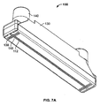
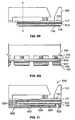
- FIGS. 7A and 7B show perspective views of a printhead module including a printing liquid supply assembly, a flexible circuit and the printhead assembly of FIG. 3A .
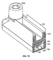
- FIG. 7C shows a perspective, cross-sectional view of the printhead module of FIG. 7B taken along line C-C.
- FIG. 7D shows a perspective, cross-sectional view of the printhead module of FIG. 7B taken along line D-D.
- FIGS. 8A-8Q illustrate a process for manufacturing a printhead body.
- FIG. 9 is a flowchart showing steps of the process illustrated in FIGS. 8A-8Q .
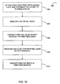
- FIG. 10 is a flowchart showing a process for assembling a printhead module.
- FIG. 11 is a cross-sectional side view of a portion of a printhead module including a cap.
- a printhead module includes pressurized pumping chambers to selectively eject a printing liquid from nozzles.
- a typical printing liquid is ink, and for illustrative purposes, the printhead module is described below in reference to ink as the printing liquid.
- the printing liquid can be other liquids, for example, electroluminescent material used in the manufacture of liquid crystal displays or liquid metals used in circuit board fabrication.
- the printhead module includes actuators that can be selectively fired to pressurize pumping chambers and eject ink from corresponding nozzles.
- an actuator is fired by applying a voltage to a piezoelectric material positioned over the pumping chamber.
- the applied voltage causes the piezoelectric material to deflect and pressurize the pumping chamber, thereby urging ink within the pumping chamber to eject from a corresponding nozzle.
- Circuitry provides drive signals to the actuator to control ejection from the nozzle.
- the piezoelectric material and at least some of the circuitry is provided on the same side of the printhead module as the nozzles.
- the printhead module can include a printhead body, a flexible circuit and an ink supply assembly.
- the printhead body 102 is formed from a base substrate 101, a nozzle plate and a piezoelectric layer.
- the base substrate 101 can be a semiconductor, e.g ., a MEMS silicon die.
- the printhead body 102 includes multiple pumping chambers 104 for holding and pumping ink through multiple nozzles (only a few of the multiple pumping chambers are illustrated), e.g ., 300 nozzles. It should be understood that more or fewer nozzle can be included.
- the pumping chambers 104 can be etched into the printhead body 102 using etching techniques known in the art.
- Each pumping chamber 104 includes an ink receiving end 106 that is in fluid communication with an ink supply, and an ink ejecting end 108 that is in fluid communication with a nozzle. Ink enters the pumping chamber 104 through an opening (not shown) in the ink receiving end 106. Upon pressurization of the pumping chamber 104 the ink is forced out the ink ejecting end 108 and ejected from the corresponding nozzle. Exemplary means for pressurizing the pumping chamber 104 to "fire" the nozzle and an exemplary ink supply assembly shall be described further below.
- a cut-away view of the printhead body 102 is shown.
- a nozzle plate 110 is shown on top of the base substrate 101, and is also shown as a cutaway view.
- the nozzle plate 110 defines multiple nozzles 112. Additionally, elongated regions of reduced thickness 114 are formed in the nozzle plate 110 positioned above the pumping chambers 104. For illustrative purposes, the regions of reduced thickness 114 are shown as openings in the nozzle plate 110, where the uppermost layer of the nozzle plate 110 has been cutaway.
- the nozzles 112 are positioned above, and are in fluid communication with, the ink ejecting ends 108 of the pumping chambers 104.
- An impedance feature 105 such as the exemplary posts depicted in FIG. 2 , can create a resistance to reduce the amount of energy going into the ink outside the pumping chamber 104 to prevent a back flow of ink from the pumping chamber 104, and to direct the flow of ink toward and through the nozzle 112.
- FIG. 3A shows a cut-away view of the printhead body 102, including a base substrate 101, a nozzle plate 110, and a piezoelectric layer 116 positioned on top of the nozzle plate 110.
- Drive contacts 122 and drive electrodes 120 are shown positioned on top of the piezoelectric layer 116.
- Each pair of drive contacts 122 and drive electrodes 120 corresponds to a pumping chamber 104 formed in the base substrate 101.
- the drive contacts 122 and drive electrodes 120 are metallic traces, e.g ., gold traces.
- the piezoelectric layer 116 is sectioned, as shown, to correspond with the positions of the pumping chambers 104.
- a ground electrode layer 117 is formed on the upper surface of the nozzle plate 110, with a cut-out region to expose the nozzles 112.
- the ground electrode layer 117 can be formed from metal, e.g ., gold, and a voltage can be applied to the ground electrode layer 117 to create a voltage differential between the ground electrode layer 117 and the drive electrodes 120.
- a drive contact 122 can receive a drive signal to apply a voltage across the piezoelectric layer 116 to fire the nozzle.
- the regions of reduced thickness 114 of the nozzle plate 110 provide a thin membrane over each of the pumping chambers 104.
- the drive signal received by the drive contact 122 causes a voltage to be applied to the drive electrode 120, thereby applying a voltage across the piezoelectric layer 116.
- a different voltage, e.g ., a lower voltage, is applied to the ground electrode layer 117.
- the voltage differential between the drive electrode 120 and the underlying region of the ground electrode layer 117 causes the piezoelectric material above a region of reduced thickness 114 in the nozzle plate to deflect and pressurize the ink in the underlying pumping chamber 104.
- FIG. 3B is a cross-sectional view of the printhead assembly of FIG. 3A taken along line A-A.
- a pumping chamber 104 is shown formed within the base substrate 101 and enclosed by the nozzle plate 110.
- the nozzle plate 110 is thinner over a substantial portion of the pumping chamber 104, in the region of reduced thickness 114.
- a nozzle 112 is formed through the nozzle plate 110 and is in fluid communication with the pumping chamber 104.
- the ground electrode layer 117 is between the nozzle plate 110 and the piezoelectric layer 116.
- a voltage can be applied to the drive electrode 120 to cause the piezoelectric layer 116 to deflect, thereby deflecting the nozzle plate 110 in the region of reduced thickness 114 and pressurizing the pumping chamber 104, forcing ink through the nozzle 112.
- FIG. 3C is a cross-sectional view of the printhead assembly of FIG. 3A taken along line B-B.
- the ground electrode layer 117 is shown layered on top of the nozzle plate 110, which is on top of the base substrate 101.
- the sectioned piezoelectric layer 116 is shown with the drive electrodes 120 layered thereon.
- FIG. 4 shows the nozzle face 124 of the printhead body 102.
- FIGS. 5A and 5B show the back face 126 of the printhead body 102.
- FIG. 5A shows the entire back face 126
- FIG. 5B shows an enlarged, end portion of the back face of the printhead body 102.
- Each ink channel 128 is in fluid communication with the pumping chambers 104 located along the corresponding side of the nozzle face 124 of the printhead body 102, by way of the openings 107 formed in the ink receiving ends 106 of the pumping chambers 104.
- each opening 107 for a pumping chamber 104 can be connected to an ink supply by an individual ink channel, rather than a shared, continuous ink channel.
- the ink channels 128 are in fluid communication with an ink supply.
- the ink supply can be positioned such that the ink path is directed from the ink supply into the openings in the ink receiving ends 106 of the pumping chambers from the back face 126 of the printhead body 102, as compared, for example, to the ink path being through the sides of the printhead body 102.
- This configuration facilitates priming of the pumping chambers 104 and nozzles 112.
- the ink travels into the pumping chambers 104 by capillary action, and the pumping chambers 104 do not have to be pressurized to move the ink from the opening in the ink receiving end 106 to fill the pumping chamber 104.
- heaters 127 can be positioned on or within the back face 126 of the printhead body 102.
- the heaters 127 can warm the printhead body 102, thereby warming the ink within the pumping chambers 104.
- a conductive material e.g ., Nichrome
- a voltage can be applied to the conductive material by electrical contacts 129 to control the temperature of the conductive material and therefore the heat emitted from the heater 127.
- the conductive material can be etched into a serpentine-like region and, optionally, the frequency of turns in the serpentine-like region can be increased toward the ends of the printhead body 102, to compensate for increased heat loss that typically occurs at the ends.
- FIG. 6 shows a flexible circuit 130 assembled with the printhead body 102.
- the flexible circuit 130 wraps around the nozzle face 124 of the printhead body 102.
- Integrated circuits 132 included on one or both wings 134 of the flexible circuit 130 connect to output leads (not shown) that extend from the corresponding integrated circuit 132 to an inner face of the flexible circuit 130 that makes contact with the nozzle face 124 of the printhead body 102.
- the output leads electrically connect to the drive contacts 122 on the piezoelectric layer 116. Drive signals can thereby be passed from an integrated circuit 132 to the drive contacts 122 by the output leads to activate the piezoelectric material and selectively fire the nozzles 112.
- the integrated circuits 132 are connected to an external source by the wings 134, which external source provides the drive signals by way of input leads (not shown) that electrically connect to the integrated circuits 132 through the flexible circuit 130.
- the external source can be a processor included in a printing device integrating the printhead module.
- there are five integrated circuits 132 each integrated circuit 132 sending signals to sixty (60) drive contacts 122 for a total of 300 drive contacts corresponding to 300 nozzles 112. More or fewer integrated circuits 132 can be used.
- circuitry can be provided directly through the flexible circuit 130 and all or some of the integrated circuits 132 can be eliminated.
- the flexible circuit 130 additionally includes tabs 136 that fold over at least one end of the printhead body 102.
- the tabs 136 electrically connect to the electrical contacts 129 to control the temperature of the heaters 127.
- FIGS. 7A-D show a printhead module 150 including an ink supply assembly 140 positioned within the flexible circuit 130 attached to the printhead body 102.
- FIG. 7A a view from the nozzle face 124 is shown.
- the flexible circuit 130 wraps around the nozzle face 124 of the printhead body 102, but includes an opening 138 to expose the nozzle plate 110 and the nozzles 112 formed therein.
- the flexible circuit 130 can be formed from a first portion that wraps around one side of the nozzle face 124 of the printhead body 102 and a second portion that wraps around the other side of the nozzle face 124 of the printhead body 102, the first and second portions not meeting on the nozzle face 124.
- FIG. 7B shows a view from the back face 126.
- one may be used as an ink inlet, e.g ., 142a, while the other, 142b, may be used as an ink outlet, if ink is recirculating through the printhead module 150.
- FIG. 7C shows a cross-sectional view of the printhead module 150 taken along line C-C shown in FIG. 7B .
- the embodiment of the ink supply assembly 140 shown includes a reservoir 144 for receiving ink.
- the reservoir 114 is formed by abutting the housing 143 of the ink supply assembly to the back face 126 of the printhead body 102.
- a filter 146 can be included in the reservoir 144 to filter contaminants from the ink before the ink is directed into the printhead body 102.
- the ink flows from the reservoir into the ink channels 128 formed in the back face 126 of the printhead body 102.
- FIG. 7D shows a cross-sectional view of the printhead module 150 taken along line D-D shown in FIG. 7B .
- the embodiment of the ink supply assembly 140 shown includes a first ink inlet 142a and a second ink inlet 142b in fluid communication with a reservoir 144.
- the reservoir 144 includes upper and lower chambers which are separated by a filter 146.
- Ink can flow freely past a support post 147. If recirculating the ink through the printhead module 150, then one of the ink inlets 142a, 142b can operate as an ink inlet and the other can operate as an ink outlet, and the support post 147 can be configured to prevent flow between the two halves of the upper chamber.
- the printhead module 150 can be manufactured according to the process described below, which includes etching flow path features in the base substrate 101 and the nozzle plate 110.
- the piezoelectric layer 116, base substrate 101 and nozzle plate 110 are bonded together to form the printhead body 102.
- a flexible circuit 130 is then attached to the printhead body 102.
- FIG. 9 is a flowchart showing the process 400 for manufacturing the printhead module 150, which is described below in reference to FIGS. 3B, 3C and 8A-Q .
- the base substrate 101 is formed from a silicon substrate 200.
- the silicon substrate 200 has a front side 210 and a back side 215, and in one embodiment has an overall thickness of about 600 microns.
- the silicon substrate 200 is piranha cleaned in a bath of sulfuric acid/hydrogen peroxide to remove organics.
- the substrate can be a silicon layer of single-crystal silicon with the plane parallel to the front and back sides 210, 215.
- the silicon substrate 200 is processed to form the pumping chambers 104 and impedance features 105 by etching through a photoresist layer that is patterned to form a mask.
- a photoresist layer that is patterned to form a mask.
- the substrate 200 is placed in hexamethyldisilazane (HMDS) fumes to prime the thermal oxide layer 203 for the photoresist layer (step 402).
- HMDS hexamethyldisilazane
- a positive photoresist layer 225 (Clariant AZ300T) is spun onto the front side 210 of the substrate 200.
- the photoresist layer 225 is soft baked, exposed with a Karl Suss through a chrome mask, and developed to form a mask defining the locations of the pumping chamber 104 and the impedance feature 105.
- the front side of the silicon substrate 200 is plasma etched by inductively coupled plasma reactive ion etching (ICP RIE) to remove exposed portions of the thermal oxide layer 203; the silicon substrate 200 is not etched.
- the silicon substrate 200 is then etched using a Bosch process deep reactive ion etching (DRIE) technique to form the pumping chamber 104 and impedance feature 105, as depicted in FIG. 8D (step 404).
- ICP RIE inductively coupled plasma reactive ion etching
- DRIE deep reactive ion etching
- a photoresist layer 239 is spun onto the back side 215 of the silicon substrate 200 and patterned to define the location of the ink channel 128.
- the thermal oxide layer 208 is removed by ICP RIE, and the silicon substrate is then etched using anisotropic etching with KOH (step 406).
- the photoresist layer 239, front oxide 203 and back oxide 208 are stripped from the substrate 200 and the substrate 200 is piranha cleaned and RCA cleaned, completing the base substrate 101 (step 408).
- a heater or heaters 127 can be formed on the back face 126 of the base substrate 101, for example, by sputtering NiChrome onto the back side 215 of the silicon substrate 200 and photolithographically etching to pattern the heaters 127.
- the nozzle plate 110 is formed from a silicon-on-insulator substrate 300 (SOI 300) (step 410).
- SOI 300 includes the nozzle silicon layer plate 110, a buried oxide layer 302 and a handle layer 306.
- tapered walls 134 and a region of reduced thickness 114 are formed by anistropically etching in the substrate 300 with KOH.
- the nozzle plate 110 can be approximately 10 microns thick.
- An aperture for the nozzle 112 is etched only part way into the nozzle plate 110, e.g ., 5 microns, and does not extend to the buried oxide layer 302.
- the SOI 300 and the base substrate 101 are aligned, and bonded to one another by annealing to create a fusion bond (step 412).
- Other bonding techniques can be used, including a layer of benzocycolbutene (BCB) adhesion promoter.
- the handle layer 306 is ground and etched and the buried oxide layer 302 is stripped from the nozzle plate 110 (step 414).
- a photoresist layer 237 is applied to the nozzle plate 110 and patterned to define the location of the nozzle 112.
- the nozzle plate 110 is etched (e.g ., DRIE) to form the nozzle opening, as shown in FIG. 8J (step 416).
- the photoresist layer 237 is stripped and the assembly of the base substrate 101 and the nozzle plate 110 is baked at 1100°C for about 4 hours to remove any polymer or organics.
- a ground electrode layer 117 is deposited on the nozzle plate 110 with a cut-out region to expose the nozzles 112.
- the ground electrode layer 117 can be formed by masking off the region including the nozzles 112 (e.g ., providing a physical barrier such as tape), and depositing a conductive material, e.g ., gold, over the exposed area of the nozzle plate 110. The mask can be removed from the region including the nozzles 112 to expose the nozzles 112.
- the piezoelectric layer 116 is formed from a block of pre-fired piezoelectric material that is about 1 mm thick (step 418).
- the block is ground to approximately 65 microns to create a planar uniform crystalline surface and cleaned in a 1% solution of fluoroboric acid (HBF 4 ) to remove surface damage caused by the grinding.
- the piezoelectric layer 116 is bonded onto a sacrificial silicon substrate 502 using a layer of BCB adhesion promoter, and cured for approximately 40 hours.
- the exposed surface of the piezoelectric layer 116 is metalized, for example, with a layer of Ti-Tungsten 512, as depicted in FIG. 8L (step 420).
- the metal layer 512 will bond and electrically connect to the metallic ground electrode layer 117 formed on the nozzle plate 110, as described above.
- a layer 514 of BCB adhesion promoter can be layered on top of the metal layer 512, to prepare the piezoelectric layer 116 for bonding to the nozzle plate 110.
- FIG. 8M shows a top view of a portion of the piezoelectric layer 116 and silicon substrate 502, after the piezoelectric layer 116 has been sectioned to create the multiple actuator portions. Each actuator portion corresponds to a separate pumping chamber 104 in the base substrate 101. Note that the entire width of the piezoelectric layer 116 is shown in FIG. 8M , as compared to the approximate half width of the piezoelectric layer shown in the cross-sectional side view of FIG. 8L .
- the piezoelectric layer 116 is not etched through to the sacrificial silicon substrate 502, but stops short approximately 10 microns.
- the piezoelectric layer 116 and the assembly of the printhead body 102 and nozzle plate 110 are aligned and brought together so that the isolation cut 148 is over the nozzle 112 and the channel cuts 503 are over the walls separating the adjacent pumping chambers 104.
- the piezoelectric layer 116 and assembly are bonded together, e.g ., in an EV bonder (step 422) to form the printhead body 102.
- the printhead body 102 is placed in a quartz oven at 200°C for 40 hours to polymerize the BCB layer 514.
- FIG. 8O shows a cross-sectional view of the assembly shown in FIG. 8N taken along line D-D along a plane going into the page.
- the channels 503 cut into the piezoelectric layer 116 are aligned with the walls separating the pumping chambers 104 formed in the printhead body 102.
- the ground electrode layer 117 can electrically connect to the metal layer 512 formed on the piezoelectric layer 116 through the BCB layer 514.
- the adhesive layer of BCB between the piezoelectric layer 116 and the sacrificial silicon substrate 502 is shown.
- the silicon handle layer 502 and part of the piezoelectric layer 116 are removed by grinding (step 424).
- the piezoelectric layer 116 is ground again and cleaned in fluoroboric acid.
- the piezoelectric layer 116 can be about 15 microns when processing is complete.
- a metal layer 118 is disposed on the exposed surface of the piezoelectric layer 116 by sputtering layers of metal, e.g ., titanium-tungsten and/or gold.
- the metal layer 118 is then photolithographically etched to form the drive contacts 122 and drive electrodes 120.
- FIG. 8Q shows a cross-sectional view of the assembly shown in FIG. 8P taken along line E-E along a plane going into the page, after the metal layer 118 has been etched to form the drive electrodes 120 and drive contacts 122.
- the piezoelectric layer 116 is sandwiched between the metal layer 512, e.g ., Ti-Tungsten, which is electrically connected to the metallic ground electrode layer 117, and the metal layer, e.g ., gold, forming the drive contacts 122 and drive electrodes 120.
- the metal layer 512 e.g ., Ti-Tungsten
- the metal layer e.g ., gold
- silicon and silicon oxide layers can be selectively etched by conventional plasma etching with commercially purchased equipment.
- the Bosch process can be used in which etching with SF 6 and C 4 F 8 alternates with depositing a polymer in 11 second cycles.
- the photoresist layer can be a commercially available positive UV photoresist system. The process can be performed at -20°C to improve the etch selectivity and prolong the useful life of the photoresist layer.
- the printhead module 150 can be assembled according to the following steps.
- the printhead body 102 i.e ., the base substrate 101, nozzle plate 110, and piezoelectric layer 116, can be connected to the flexible circuit 130 (step 602). Electrical tests can be executed to ensure that signals are passing from the flexible circuit 130 to the printhead body 102 (step 604).
- the ink supply assembly 140 is connected to the printhead body 102, with the flexible circuit 130 attached (step 606) to complete the printhead module 150. Pressure and leak tests can be executed to ensure that ink is traveling through the printhead module 150 without leakage (step 608).
- Printing tests can be executed to ensure that the printhead module 150 prints ink as required (step 610).
- a printhead module 518 can include a silicon cap 520 formed over the nozzle face and piezoelectric layer 116.
- the silicon cap 520 is thicker and more robust than the relatively thin silicon membrane formed over the pumping chambers 104 and piezoelectric layer 116, providing a protective cover.
- FIG. 11 shows a cross-sectional side view of a portion of a printhead module 518, similar to the view shown in FIG. 8P .
- a via (through hole) 522 is formed through the silicon cap 520 to the drive contact 122.
- the via is coated with a conductive material to provide an electrical connection between the drive contact 122 and a flexible circuit that can be connected to the exterior of the silicon cap 520, to provide signals to the drive contact 122.
- a recess 524 is formed in the silicon cap 520 to provide room for the piezoelectric layer 116 to flex when actuated by the drive contact 122 and drive electrode 120.
- a heater 526 e.g ., a Nichrome heater, can be included within the recess 524, which can be in addition to or instead of another heater included in the module.
- the shape of the nozzle can be determined by the shape of the passage 528 through the silicon cap 520.
- the nozzle can be formed in the silicon cap 520, in which case the passage 528 would be wider to be consistent with the width at the inner portion of the nozzle.
- the silicon cap 520 can be formed using etching techniques, including those described above, and adhered to the nozzle face of the printhead module 518.
- ink is just one example of a printing liquid. It should be understood that reference about to ink as the printing liquid was for illustrative purposes only, and referring to components within the printhead module described above with the adjective "ink” was also illustrative. That is, referring to a channel or a supply assembly as an "ink channel” or an “ink supply assembly” was for illustrative purposes, and a more general reference, such as to a “printing liquid channel” or a “printing liquid supply assembly” can be used. Further, the use of terminology such as “front” and “back” and “top” and “bottom” throughout the specification and claims is for illustrative purposes only, to distinguish between various components of the printhead module and other elements described herein. The use of “front” and “back” and “top” and “bottom” does not imply a particular orientation of the printhead module.
Landscapes
- Engineering & Computer Science (AREA)
- Manufacturing & Machinery (AREA)
- Particle Formation And Scattering Control In Inkjet Printers (AREA)
- Ink Jet (AREA)
- Recording Measured Values (AREA)
Abstract
Description
- The following description relates to a printhead assembly including one or more nozzles.
- An ink jet printer typically includes an ink path from an ink supply to an ink nozzle assembly that includes nozzles from which ink drops are ejected. Ink drop ejection can be controlled by pressurizing ink in the ink path with an actuator, which may be, for example, a piezoelectric deflector, a thermal bubble jet generator, or an electrostatically deflected element. A typical printhead has a line of nozzles with a corresponding array of ink paths and associated actuators, and drop ejection from each nozzle can be independently controlled. In a so-called "drop-on-demand" printhead, each actuator is fired to selectively eject a drop at a specific pixel location of an image, as the printhead and a printing media are moved relative to one another. In high performance printheads, the nozzles typically have a diameter of 50 microns or less (e.g., 25 microns), are separated at a pitch of 100-300 nozzles per inch and provide drop sizes of approximately 1 to 70 picoliters (pl) or less. Drop ejection frequency is typically 10 kHz or more.
- A printhead can include a semiconductor printhead body and a piezoelectric actuator, for example, the printhead described in
Hoisington et al., U.S. Patent No. 5,265,315 . The printhead body can be made of silicon, which is etched to define ink chambers. Nozzles can be defined by a separate nozzle plate that is attached to the silicon body. The piezoelectric actuator can have a layer of piezoelectric material that changes geometry, or bends, in response to an applied voltage. The bending of the piezoelectric layer pressurizes ink in a pumping chamber located along the ink path. - Printing accuracy can be influenced by a number of factors, including the uniformity in size and velocity of ink drops ejected by the nozzles in the printhead and among the multiple printheads in a printer. The drop size and drop velocity uniformity are in turn influenced by factors, such as the dimensional uniformity of the ink paths, acoustic interference effects, contamination in the ink flow paths, and the uniformity of the pressure pulse generated by the actuators. Contamination or debris in the ink flow can be reduced with the use of one or more filters in the ink flow path.
EP 1 101 615 discloses the preamble of claim 1. - A printhead assembly including one or more nozzles is described. In general, in one aspect, the invention features a printhead module including a printhead body, a nozzle plate and one or more piezoelectric actuators. The printhead body includes one or more pumping chambers, where each pumping chamber includes a receiving end configured to receive a printing liquid from a printing liquid supply and an ejecting end for ejecting the printing liquid from the pumping chamber. The nozzle plate includes one or more nozzles formed through the nozzle plate. Each nozzle is in fluid communication with a pumping chamber and receives printing liquid from the ejecting end of the pumping chamber for ejection from the nozzle. The one or more piezoelectric actuators are connected to the nozzle plate. A piezoelectric actuator is positioned over each pumping chamber and includes a piezoelectric material configured to deflect and pressurize the pumping chamber, so as to eject printing liquid from a corresponding nozzle that is in fluid communication with the ejecting end of the pumping chamber.
- Implementations of the invention can include one or more of the following features. The printhead module can be included in a printhead system that includes a flexible circuit connected to a nozzle face of the printhead module. The flexible circuit is electrically coupled to the one or more piezoelectric actuators so as to provide signals to the one or more piezoelectric actuators to selectively pressurize the one or more pumping chambers to fire the one or more corresponding nozzles.
- The printhead module can include a cap attached to the nozzle plate and including one or more apertures connecting to the one or more nozzles formed through the nozzle plate. The cap is configured to cover the one or more piezoelectric actuators while providing sufficient clearance for the piezoelectric material included in the one or more actuators to deflect when actuated.
- The printhead module can include a printing liquid supply assembly, where the printing liquid supply assembly includes a reservoir in fluid communication with the receiving end of the pumping chamber. The printhead body can include a back face that is substantially parallel to a nozzle face which connects to the nozzle plate. The printing liquid supply assembly can be connected to the back face of the printhead body, and the receiving end of the pumping chamber can include an opening on the back face of the printhead body in fluid communication with the reservoir.
- The printhead module can include a plurality of pumping chambers and further include at least one printing liquid channel formed in the back face of the printhead body. The printing liquid channel is in fluid communication with openings of the pumping chambers and with the reservoir. The printing liquid enters the printing liquid channel from the reservoir and is directed into the openings of the pumping chambers. In one implementation, the printing liquid channel includes at least two sides angled toward the openings of the pumping chambers.
- The invention can be implemented to realize one or more of the following advantages. The printhead module can be fabricated using less silicon and with fewer fabrication steps then prior art printhead modules, for example, printhead modules incorporating a piezoelectric layer on the back face of the printhead body, as compared to the nozzle face of the printhead body. The required etch time can be reduced, thereby reducing the fabrication time. For example, ink channels included in the printhead module can be etched using a KOH etching process as compared to the more time-consuming Bosch process. Positioning the piezoelectric layer on the nozzle face of the printhead body can free up the back face of the printhead body for other features. For example, a heater can be integrated into the back face of the printhead body.
- An ink supply can feed ink into the pumping chambers included in the printhead body from the back face, as compared to along a side of the printhead body. Feeding ink from the back face of the printhead body into the pumping chambers facilitates priming the pumping chambers, as the pumping chambers can fill by capillary action. Additionally, a length of a path from the ink supply into the pumping chamber can be shorter than if the ink enters through the side of the pumping chamber, thereby providing an improved frequency of response. Further, bonding the printhead module to a housing is facilitated by having the ink channels on the back face as compared to the sides, as an adhesive can be used along the sides without risk of the adhesive entering the ink channels. The printhead module can be fabricated from fewer layers, thereby reducing thickness variations across the module.
- Details of one or more implementations are set forth in the accompanying drawings and the description below. Other features and advantages may be apparent from the description and drawings, and from the claims.
- These and other aspects will now be described in detail with reference to the following drawings.
-
FIG. 1 shows a portion of a printhead body. -
FIG. 2 shows a cutaway view of the portion of the printhead body ofFIG. 1 with a cutaway view of a portion of a nozzle plate on top of the printhead body. -
FIG. 3A shows a portion of a printhead assembly including a portion of a piezoelectric layer with electrical connectors thereon on top of the portion of the printhead body and nozzle plate shown inFIG. 2 . -
FIG. 3B is a cross-sectional view of the printhead assembly ofFIG. 3A taken along line A-A. -
FIG. 3C is a cross-sectional view of the printhead assembly ofFIG. 3A taken along line B-B. -
FIG. 4 shows a nozzle face of the printhead assembly ofFIG. 3A . -
FIG. 5A shows a back face of the printhead assembly ofFIG. 3A . -
FIG. 5B shows an enlarged portion of the back face shown inFIG. 5A . -
FIG. 6 shows a flexible circuit attached to the printhead assembly ofFIG. 3A . -
FIGS. 7A and7B show perspective views of a printhead module including a printing liquid supply assembly, a flexible circuit and the printhead assembly ofFIG. 3A . -
FIG. 7C shows a perspective, cross-sectional view of the printhead module ofFIG. 7B taken along line C-C. -
FIG. 7D shows a perspective, cross-sectional view of the printhead module ofFIG. 7B taken along line D-D. -
FIGS. 8A-8Q illustrate a process for manufacturing a printhead body. -
FIG. 9 is a flowchart showing steps of the process illustrated inFIGS. 8A-8Q . -
FIG. 10 is a flowchart showing a process for assembling a printhead module. -
FIG. 11 is a cross-sectional side view of a portion of a printhead module including a cap. - Like reference symbols in the various drawings indicate like elements.
- A printhead module is described that includes pressurized pumping chambers to selectively eject a printing liquid from nozzles. A typical printing liquid is ink, and for illustrative purposes, the printhead module is described below in reference to ink as the printing liquid. However, it should be understood that the printing liquid can be other liquids, for example, electroluminescent material used in the manufacture of liquid crystal displays or liquid metals used in circuit board fabrication.
- The printhead module includes actuators that can be selectively fired to pressurize pumping chambers and eject ink from corresponding nozzles. For example, in one embodiment an actuator is fired by applying a voltage to a piezoelectric material positioned over the pumping chamber. The applied voltage causes the piezoelectric material to deflect and pressurize the pumping chamber, thereby urging ink within the pumping chamber to eject from a corresponding nozzle. Circuitry provides drive signals to the actuator to control ejection from the nozzle. The piezoelectric material and at least some of the circuitry is provided on the same side of the printhead module as the nozzles. The printhead module can include a printhead body, a flexible circuit and an ink supply assembly.
- Referring to
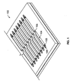
FIG. 1 , a portion of an embodiment of aprinthead body 102 is shown. Theprinthead body 102 is formed from abase substrate 101, a nozzle plate and a piezoelectric layer. Thebase substrate 101 can be a semiconductor, e.g., a MEMS silicon die. In the embodiment shown, theprinthead body 102 includesmultiple pumping chambers 104 for holding and pumping ink through multiple nozzles (only a few of the multiple pumping chambers are illustrated), e.g., 300 nozzles. It should be understood that more or fewer nozzle can be included. - The pumping
chambers 104 can be etched into theprinthead body 102 using etching techniques known in the art. Eachpumping chamber 104 includes anink receiving end 106 that is in fluid communication with an ink supply, and anink ejecting end 108 that is in fluid communication with a nozzle. Ink enters thepumping chamber 104 through an opening (not shown) in theink receiving end 106. Upon pressurization of thepumping chamber 104 the ink is forced out theink ejecting end 108 and ejected from the corresponding nozzle. Exemplary means for pressurizing thepumping chamber 104 to "fire" the nozzle and an exemplary ink supply assembly shall be described further below. - Referring to
FIG. 2 , a cut-away view of theprinthead body 102 is shown. Anozzle plate 110 is shown on top of thebase substrate 101, and is also shown as a cutaway view. Thenozzle plate 110 definesmultiple nozzles 112. Additionally, elongated regions of reducedthickness 114 are formed in thenozzle plate 110 positioned above the pumpingchambers 104. For illustrative purposes, the regions of reducedthickness 114 are shown as openings in thenozzle plate 110, where the uppermost layer of thenozzle plate 110 has been cutaway. Thenozzles 112 are positioned above, and are in fluid communication with, the ink ejecting ends 108 of the pumpingchambers 104. Animpedance feature 105, such as the exemplary posts depicted inFIG. 2 , can create a resistance to reduce the amount of energy going into the ink outside thepumping chamber 104 to prevent a back flow of ink from thepumping chamber 104, and to direct the flow of ink toward and through thenozzle 112. -
FIG. 3A shows a cut-away view of theprinthead body 102, including abase substrate 101, anozzle plate 110, and apiezoelectric layer 116 positioned on top of thenozzle plate 110. Drivecontacts 122 and driveelectrodes 120 are shown positioned on top of thepiezoelectric layer 116. Each pair ofdrive contacts 122 and driveelectrodes 120 corresponds to apumping chamber 104 formed in thebase substrate 101. In one embodiment, thedrive contacts 122 and driveelectrodes 120 are metallic traces, e.g., gold traces. Thepiezoelectric layer 116 is sectioned, as shown, to correspond with the positions of the pumpingchambers 104. Aground electrode layer 117 is formed on the upper surface of thenozzle plate 110, with a cut-out region to expose thenozzles 112. Theground electrode layer 117 can be formed from metal, e.g., gold, and a voltage can be applied to theground electrode layer 117 to create a voltage differential between theground electrode layer 117 and thedrive electrodes 120. - A
drive contact 122 can receive a drive signal to apply a voltage across thepiezoelectric layer 116 to fire the nozzle. The regions of reducedthickness 114 of thenozzle plate 110 provide a thin membrane over each of the pumpingchambers 104. The drive signal received by thedrive contact 122 causes a voltage to be applied to thedrive electrode 120, thereby applying a voltage across thepiezoelectric layer 116. A different voltage, e.g., a lower voltage, is applied to theground electrode layer 117. The voltage differential between thedrive electrode 120 and the underlying region of theground electrode layer 117 causes the piezoelectric material above a region of reducedthickness 114 in the nozzle plate to deflect and pressurize the ink in theunderlying pumping chamber 104. -
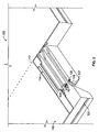
FIG. 3B is a cross-sectional view of the printhead assembly ofFIG. 3A taken along line A-A. Apumping chamber 104 is shown formed within thebase substrate 101 and enclosed by thenozzle plate 110. Thenozzle plate 110 is thinner over a substantial portion of thepumping chamber 104, in the region of reducedthickness 114. Anozzle 112 is formed through thenozzle plate 110 and is in fluid communication with thepumping chamber 104. Theground electrode layer 117 is between thenozzle plate 110 and thepiezoelectric layer 116. As described above, a voltage can be applied to thedrive electrode 120 to cause thepiezoelectric layer 116 to deflect, thereby deflecting thenozzle plate 110 in the region of reducedthickness 114 and pressurizing thepumping chamber 104, forcing ink through thenozzle 112. - An
opening 107 in theink receiving end 106 of the pumping chamber is shown. A trough-like ink channel 128 leads into theopening 107, to supply ink to thepumping chamber 104. Theink channel 128 receives ink from an ink supply, described further below.FIG. 3C is a cross-sectional view of the printhead assembly ofFIG. 3A taken along line B-B. Theground electrode layer 117 is shown layered on top of thenozzle plate 110, which is on top of thebase substrate 101. The sectionedpiezoelectric layer 116 is shown with thedrive electrodes 120 layered thereon. -
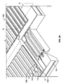
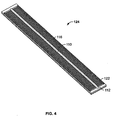
FIG. 4 shows thenozzle face 124 of theprinthead body 102.FIGS. 5A and5B show theback face 126 of theprinthead body 102.FIG. 5A shows theentire back face 126, whileFIG. 5B shows an enlarged, end portion of the back face of theprinthead body 102. Along the length of both sides of theback face 126 of theprinthead body 102 are two trough-like ink channels 128. Eachink channel 128 is in fluid communication with the pumpingchambers 104 located along the corresponding side of thenozzle face 124 of theprinthead body 102, by way of theopenings 107 formed in the ink receiving ends 106 of the pumpingchambers 104. Other configurations of theink channels 128 can be used, for example, with curved surfaces. The trough-like configuration directs ink toward the openings in the ink receiving ends 106 of the pumpingchambers 104. Alternatively, each opening 107 for apumping chamber 104 can be connected to an ink supply by an individual ink channel, rather than a shared, continuous ink channel. - The
ink channels 128 are in fluid communication with an ink supply. The ink supply can be positioned such that the ink path is directed from the ink supply into the openings in the ink receiving ends 106 of the pumping chambers from theback face 126 of theprinthead body 102, as compared, for example, to the ink path being through the sides of theprinthead body 102. This configuration facilitates priming of the pumpingchambers 104 andnozzles 112. In one implementation, the ink travels into the pumpingchambers 104 by capillary action, and the pumpingchambers 104 do not have to be pressurized to move the ink from the opening in theink receiving end 106 to fill thepumping chamber 104. - Optionally,
heaters 127 can be positioned on or within theback face 126 of theprinthead body 102. Theheaters 127 can warm theprinthead body 102, thereby warming the ink within the pumpingchambers 104. In one embodiment, as shown inFIGS. 5A and5B , a conductive material, e.g., Nichrome, can be sputtered onto theback face 126 of theprinthead body 102 and photolithographically etched into a desired pattern, such as the elongated regions shown. A voltage can be applied to the conductive material byelectrical contacts 129 to control the temperature of the conductive material and therefore the heat emitted from theheater 127. In another embodiment, the conductive material can be etched into a serpentine-like region and, optionally, the frequency of turns in the serpentine-like region can be increased toward the ends of theprinthead body 102, to compensate for increased heat loss that typically occurs at the ends. -
FIG. 6 shows aflexible circuit 130 assembled with theprinthead body 102. Theflexible circuit 130 wraps around thenozzle face 124 of theprinthead body 102.Integrated circuits 132 included on one or bothwings 134 of theflexible circuit 130 connect to output leads (not shown) that extend from the correspondingintegrated circuit 132 to an inner face of theflexible circuit 130 that makes contact with thenozzle face 124 of theprinthead body 102. The output leads electrically connect to thedrive contacts 122 on thepiezoelectric layer 116. Drive signals can thereby be passed from anintegrated circuit 132 to thedrive contacts 122 by the output leads to activate the piezoelectric material and selectively fire thenozzles 112. - The
integrated circuits 132 are connected to an external source by thewings 134, which external source provides the drive signals by way of input leads (not shown) that electrically connect to theintegrated circuits 132 through theflexible circuit 130. For example, the external source can be a processor included in a printing device integrating the printhead module. In one embodiment, there are fiveintegrated circuits 132, eachintegrated circuit 132 sending signals to sixty (60) drivecontacts 122 for a total of 300 drive contacts corresponding to 300nozzles 112. More or fewerintegrated circuits 132 can be used. Alternatively, for a printhead module including relatively few nozzles, circuitry can be provided directly through theflexible circuit 130 and all or some of theintegrated circuits 132 can be eliminated. - In one implementation, the
flexible circuit 130 additionally includestabs 136 that fold over at least one end of theprinthead body 102. Thetabs 136 electrically connect to theelectrical contacts 129 to control the temperature of theheaters 127. -
FIGS. 7A-D show aprinthead module 150 including anink supply assembly 140 positioned within theflexible circuit 130 attached to theprinthead body 102. Referring toFIG. 7A , a view from thenozzle face 124 is shown. Theflexible circuit 130 wraps around thenozzle face 124 of theprinthead body 102, but includes anopening 138 to expose thenozzle plate 110 and thenozzles 112 formed therein. Alternatively, theflexible circuit 130 can be formed from a first portion that wraps around one side of thenozzle face 124 of theprinthead body 102 and a second portion that wraps around the other side of thenozzle face 124 of theprinthead body 102, the first and second portions not meeting on thenozzle face 124. Thenozzles 112 formed on thenozzle plate 110 are therefore exposed between the first and second portions of theflexible circuit 130.FIG. 7B shows a view from theback face 126. In the embodiment of theink supply assembly 140 shown, there are twoink inlets printhead module 150. -
FIG. 7C shows a cross-sectional view of theprinthead module 150 taken along line C-C shown inFIG. 7B . The embodiment of theink supply assembly 140 shown includes areservoir 144 for receiving ink. Thereservoir 114 is formed by abutting the housing 143 of the ink supply assembly to theback face 126 of theprinthead body 102. Afilter 146 can be included in thereservoir 144 to filter contaminants from the ink before the ink is directed into theprinthead body 102. The ink flows from the reservoir into theink channels 128 formed in theback face 126 of theprinthead body 102. -
FIG. 7D shows a cross-sectional view of theprinthead module 150 taken along line D-D shown inFIG. 7B . The embodiment of theink supply assembly 140 shown includes afirst ink inlet 142a and asecond ink inlet 142b in fluid communication with areservoir 144. Thereservoir 144 includes upper and lower chambers which are separated by afilter 146. Ink can flow freely past a support post 147. If recirculating the ink through theprinthead module 150, then one of theink inlets - The
printhead module 150 can be manufactured according to the process described below, which includes etching flow path features in thebase substrate 101 and thenozzle plate 110. Thepiezoelectric layer 116,base substrate 101 andnozzle plate 110 are bonded together to form theprinthead body 102. Aflexible circuit 130 is then attached to theprinthead body 102.FIG. 9 is a flowchart showing theprocess 400 for manufacturing theprinthead module 150, which is described below in reference toFIGS. 3B, 3C and8A-Q . - Referring to
FIG. 8A , thebase substrate 101 is formed from asilicon substrate 200. Thesilicon substrate 200 has afront side 210 and aback side 215, and in one embodiment has an overall thickness of about 600 microns. There are thermal oxide layers 203, 208, each about 1 micron thick, on thefront side 210 and backside 215 of thesubstrate 200. Thesilicon substrate 200 is piranha cleaned in a bath of sulfuric acid/hydrogen peroxide to remove organics. The substrate can be a silicon layer of single-crystal silicon with the plane parallel to the front andback sides - The
silicon substrate 200 is processed to form the pumpingchambers 104 and impedance features 105 by etching through a photoresist layer that is patterned to form a mask. To prepare thesilicon substrate 200 for the photoresist layer, thesubstrate 200 is placed in hexamethyldisilazane (HMDS) fumes to prime thethermal oxide layer 203 for the photoresist layer (step 402). Referring toFIG. 8B , a positive photoresist layer 225 (Clariant AZ300T) is spun onto thefront side 210 of thesubstrate 200. Thephotoresist layer 225 is soft baked, exposed with a Karl Suss through a chrome mask, and developed to form a mask defining the locations of thepumping chamber 104 and theimpedance feature 105. - Referring to
FIG. 8C , the front side of thesilicon substrate 200 is plasma etched by inductively coupled plasma reactive ion etching (ICP RIE) to remove exposed portions of thethermal oxide layer 203; thesilicon substrate 200 is not etched. Thesilicon substrate 200 is then etched using a Bosch process deep reactive ion etching (DRIE) technique to form thepumping chamber 104 andimpedance feature 105, as depicted inFIG. 8D (step 404). - Referring to
FIG. 8E , aphotoresist layer 239 is spun onto theback side 215 of thesilicon substrate 200 and patterned to define the location of theink channel 128. Thethermal oxide layer 208 is removed by ICP RIE, and the silicon substrate is then etched using anisotropic etching with KOH (step 406). Referring toFIG. 8F , thephotoresist layer 239,front oxide 203 andback oxide 208 are stripped from thesubstrate 200 and thesubstrate 200 is piranha cleaned and RCA cleaned, completing the base substrate 101 (step 408). Optionally, a heater orheaters 127 can be formed on theback face 126 of thebase substrate 101, for example, by sputtering NiChrome onto theback side 215 of thesilicon substrate 200 and photolithographically etching to pattern theheaters 127. - Referring to
FIG. 8G , thenozzle plate 110 is formed from a silicon-on-insulator substrate 300 (SOI 300) (step 410). TheSOI 300 includes the nozzlesilicon layer plate 110, a buriedoxide layer 302 and ahandle layer 306. Before bonding theSOI 300 to thebase substrate 101, taperedwalls 134 and a region of reducedthickness 114 are formed by anistropically etching in thesubstrate 300 with KOH. In one embodiment, thenozzle plate 110 can be approximately 10 microns thick. An aperture for thenozzle 112 is etched only part way into thenozzle plate 110, e.g., 5 microns, and does not extend to the buriedoxide layer 302. - Referring to
FIG. 8H , theSOI 300 and thebase substrate 101 are aligned, and bonded to one another by annealing to create a fusion bond (step 412). Other bonding techniques can be used, including a layer of benzocycolbutene (BCB) adhesion promoter. Referring toFIG. 8I , thehandle layer 306 is ground and etched and the buriedoxide layer 302 is stripped from the nozzle plate 110 (step 414). Aphotoresist layer 237 is applied to thenozzle plate 110 and patterned to define the location of thenozzle 112. Thenozzle plate 110 is etched (e.g., DRIE) to form the nozzle opening, as shown inFIG. 8J (step 416). Thephotoresist layer 237 is stripped and the assembly of thebase substrate 101 and thenozzle plate 110 is baked at 1100°C for about 4 hours to remove any polymer or organics. - Referring to
FIG. 8K , aground electrode layer 117 is deposited on thenozzle plate 110 with a cut-out region to expose thenozzles 112. In one implementation, theground electrode layer 117 can be formed by masking off the region including the nozzles 112 (e.g., providing a physical barrier such as tape), and depositing a conductive material, e.g., gold, over the exposed area of thenozzle plate 110. The mask can be removed from the region including thenozzles 112 to expose thenozzles 112. - Referring to
FIG. 8L , thepiezoelectric layer 116 is formed from a block of pre-fired piezoelectric material that is about 1 mm thick (step 418). The block is ground to approximately 65 microns to create a planar uniform crystalline surface and cleaned in a 1% solution of fluoroboric acid (HBF4) to remove surface damage caused by the grinding. Thepiezoelectric layer 116 is bonded onto asacrificial silicon substrate 502 using a layer of BCB adhesion promoter, and cured for approximately 40 hours. - The exposed surface of the
piezoelectric layer 116 is metalized, for example, with a layer of Ti-Tungsten 512, as depicted inFIG. 8L (step 420). Themetal layer 512 will bond and electrically connect to the metallicground electrode layer 117 formed on thenozzle plate 110, as described above. Alayer 514 of BCB adhesion promoter can be layered on top of themetal layer 512, to prepare thepiezoelectric layer 116 for bonding to thenozzle plate 110. - Before bonding the
piezoelectric layer 116 to thenozzle plate 110, the piezoelectric material is sectioned to create multiple actuator portions (step 420).FIG. 8M shows a top view of a portion of thepiezoelectric layer 116 andsilicon substrate 502, after thepiezoelectric layer 116 has been sectioned to create the multiple actuator portions. Each actuator portion corresponds to aseparate pumping chamber 104 in thebase substrate 101. Note that the entire width of thepiezoelectric layer 116 is shown inFIG. 8M , as compared to the approximate half width of the piezoelectric layer shown in the cross-sectional side view ofFIG. 8L . To form the actuator portions, cuts are made in the piezoelectric material to form anisolation area 148 above the region that will correspond to thenozzles 112 formed in thenozzle plate 112 and to form thechannels 503. Thepiezoelectric layer 116 is not etched through to thesacrificial silicon substrate 502, but stops short approximately 10 microns. - Referring to
FIG. 8N , thepiezoelectric layer 116 and the assembly of theprinthead body 102 and nozzle plate 110 (withground electrode layer 117 thereon) are aligned and brought together so that the isolation cut 148 is over thenozzle 112 and the channel cuts 503 are over the walls separating theadjacent pumping chambers 104. Thepiezoelectric layer 116 and assembly are bonded together, e.g., in an EV bonder (step 422) to form theprinthead body 102. Theprinthead body 102 is placed in a quartz oven at 200°C for 40 hours to polymerize theBCB layer 514. -
FIG. 8O shows a cross-sectional view of the assembly shown inFIG. 8N taken along line D-D along a plane going into the page. Thechannels 503 cut into thepiezoelectric layer 116 are aligned with the walls separating the pumpingchambers 104 formed in theprinthead body 102. Theground electrode layer 117 can electrically connect to themetal layer 512 formed on thepiezoelectric layer 116 through theBCB layer 514. In this view, the adhesive layer of BCB between thepiezoelectric layer 116 and thesacrificial silicon substrate 502 is shown. - Referring to
FIG. 8P , thesilicon handle layer 502 and part of thepiezoelectric layer 116 are removed by grinding (step 424). Thepiezoelectric layer 116 is ground again and cleaned in fluoroboric acid. Thepiezoelectric layer 116 can be about 15 microns when processing is complete. Ametal layer 118 is disposed on the exposed surface of thepiezoelectric layer 116 by sputtering layers of metal, e.g., titanium-tungsten and/or gold. Themetal layer 118 is then photolithographically etched to form thedrive contacts 122 and driveelectrodes 120. -
FIG. 8Q shows a cross-sectional view of the assembly shown inFIG. 8P taken along line E-E along a plane going into the page, after themetal layer 118 has been etched to form thedrive electrodes 120 and drivecontacts 122. Thepiezoelectric layer 116 is sandwiched between themetal layer 512, e.g., Ti-Tungsten, which is electrically connected to the metallicground electrode layer 117, and the metal layer, e.g., gold, forming thedrive contacts 122 and driveelectrodes 120. By applying different voltages to theground electrode layer 117 and thedrive electrode 120, a region of thepiezoelectric layer 116 over apumping chamber 104 can be actuated. That is, the voltage differential can cause thepiezoelectric layer 116 to flex, thereby pressurizing the ink in thepumping chamber 104. - In general, silicon and silicon oxide layers can be selectively etched by conventional plasma etching with commercially purchased equipment. For silicon etching features with straight side walls, the Bosch process can be used in which etching with SF6 and C4F8 alternates with depositing a polymer in 11 second cycles. The photoresist layer can be a commercially available positive UV photoresist system. The process can be performed at -20°C to improve the etch selectivity and prolong the useful life of the photoresist layer.
- Referring to
FIG. 10 , theprinthead module 150 can be assembled according to the following steps. Theprinthead body 102, i.e., thebase substrate 101,nozzle plate 110, andpiezoelectric layer 116, can be connected to the flexible circuit 130 (step 602). Electrical tests can be executed to ensure that signals are passing from theflexible circuit 130 to the printhead body 102 (step 604). Theink supply assembly 140 is connected to theprinthead body 102, with theflexible circuit 130 attached (step 606) to complete theprinthead module 150. Pressure and leak tests can be executed to ensure that ink is traveling through theprinthead module 150 without leakage (step 608). i Printing tests can be executed to ensure that theprinthead module 150 prints ink as required (step 610). - Referring to
FIG. 11 , in another embodiment, aprinthead module 518 can include asilicon cap 520 formed over the nozzle face andpiezoelectric layer 116. Thesilicon cap 520 is thicker and more robust than the relatively thin silicon membrane formed over the pumpingchambers 104 andpiezoelectric layer 116, providing a protective cover.FIG. 11 shows a cross-sectional side view of a portion of aprinthead module 518, similar to the view shown inFIG. 8P . A via (through hole) 522 is formed through thesilicon cap 520 to thedrive contact 122. The via is coated with a conductive material to provide an electrical connection between thedrive contact 122 and a flexible circuit that can be connected to the exterior of thesilicon cap 520, to provide signals to thedrive contact 122. Arecess 524 is formed in thesilicon cap 520 to provide room for thepiezoelectric layer 116 to flex when actuated by thedrive contact 122 and driveelectrode 120. Optionally, aheater 526, e.g., a Nichrome heater, can be included within therecess 524, which can be in addition to or instead of another heater included in the module. The shape of the nozzle can be determined by the shape of thepassage 528 through thesilicon cap 520. In one implementation, the nozzle can be formed in thesilicon cap 520, in which case thepassage 528 would be wider to be consistent with the width at the inner portion of the nozzle. Thesilicon cap 520 can be formed using etching techniques, including those described above, and adhered to the nozzle face of theprinthead module 518. - As previously mentioned, ink is just one example of a printing liquid. It should be understood that reference about to ink as the printing liquid was for illustrative purposes only, and referring to components within the printhead module described above with the adjective "ink" was also illustrative. That is, referring to a channel or a supply assembly as an "ink channel" or an "ink supply assembly" was for illustrative purposes, and a more general reference, such as to a "printing liquid channel" or a "printing liquid supply assembly" can be used. Further, the use of terminology such as "front" and "back" and "top" and "bottom" throughout the specification and claims is for illustrative purposes only, to distinguish between various components of the printhead module and other elements described herein. The use of "front" and "back" and "top" and "bottom" does not imply a particular orientation of the printhead module.
- Although only a few embodiments have been described in detail above, other modifications are possible. Other embodiments may be within the scope of the following claims.
Claims (5)
- A printhead module (150, 518), comprising:a printhead body (102) including one or more pumping chambers (104), where each pumping chamber (104) includes a receiving end (106) configured to receive a printing liquid from a printing liquid supply and an ejecting end (108) for ejecting the printing liquid from the pumping chamber (104);a nozzle plate (110) enclosing the one or more pumping chambers (104), the nozzle plate (110) including one or more nozzles (122) formed through the nozzle plate (110), where a nozzle (112) is in fluid communication with each pumping chamber (104) and receives printing liquid from the ejecting end (108) of the pumping chamber (104) for ejection from the nozzle (112); andone or more piezoelectric actuators connected to the nozzle plate (110), where a piezoelectric actuator is positioned over each pumping chamber (104), and where each piezoelectric actuator includes a ground electrode (117), a drive electrode (120) and a piezoelectric material (116) configured to deflect and pressurize the pumping chamber (104), so as to eject printing liquid from a corresponding nozzle (112) that is in fluid communication with the ejecting end (108) of the pumping chamber (104), and where the piezoelectric material (116) is positioned between the ground electrode (117) and the drive electrode (120);characterized in thatthe nozzle plate (110) is arranged between the pumping chambers (104) on the one side and the piezoelectric actuators on the other side and includes a region of reduced thickness positioned over each of the one or more pumping chambers (104).
- The printhead module of claim 1, further comprising:a printing liquid supply assembly (140), where the printing liquid supply assembly (140) includes a reservoir (144) in fluid communication with the receiving end (106) of the pumping chamber (104);wherein:the printhead body (102) includes a back face (126) that is substantially parallel to a nozzle face (124) which connects to the nozzle plate (110);the printing liquid supply assembly (140) is connected to the back face (126) of the printhead body (102); andthe receiving end (106) of the pumping chamber (104) includes an opening (107) on the back face (126) of the printhead body in fluid communication with the reservoir (144).
- The printhead module of claim 2, wherein the printhead module includes a plurality of pumping chambers (104), the printhead module further comprising:at least one printing liquid channel (128) formed in the back face (126) of the printhead body (102), the at least one printing liquid channel (128) in fluid communication with openings (107) of a plurality of pumping chambers (104) and with the reservoir (144), where printing liquid enters the at least one printing liquid channel (128) from the reservoir (144) and is directed into the openings (107) of the plurality of pumping chambers (104).
- The printhead module of claim 3, wherein the at least one printing liquid channel (128) includes at least two sides angled toward the openings (107) of the plurality of pumping chambers (104).
- A printhead system comprising:a printhead module according to claim 1 having a nozzle face (124) and a back face (126) substantially parallel to and opposite the nozzle face (124), the printhead module (150, 518) including:a flexible circuit (130) connected to the nozzle face (124) of the printhead module and electrically coupled to the one or more piezoelectric actuators so as to provide signals to the one or more piezoelectric actuators to selectively pressurize the one or more pumping chambers (104) to fire the one or more corresponding nozzles (112).
Applications Claiming Priority (3)
| Application Number | Priority Date | Filing Date | Title |
|---|---|---|---|
| US63725404P | 2004-12-17 | 2004-12-17 | |
| US69913405P | 2005-07-13 | 2005-07-13 | |
| PCT/US2005/045672 WO2006066102A1 (en) | 2004-12-17 | 2005-12-16 | Printhead module |
Publications (2)
| Publication Number | Publication Date |
|---|---|
| EP1848592A1 EP1848592A1 (en) | 2007-10-31 |
| EP1848592B1 true EP1848592B1 (en) | 2011-09-28 |
Family
ID=36177858
Family Applications (2)
| Application Number | Title | Priority Date | Filing Date |
|---|---|---|---|
| EP05854598A Active EP1831026B1 (en) | 2004-12-17 | 2005-12-16 | Single-use droplet ejection module |
| EP05854400A Active EP1848592B1 (en) | 2004-12-17 | 2005-12-16 | Printhead module |
Family Applications Before (1)
| Application Number | Title | Priority Date | Filing Date |
|---|---|---|---|
| EP05854598A Active EP1831026B1 (en) | 2004-12-17 | 2005-12-16 | Single-use droplet ejection module |
Country Status (9)
| Country | Link |
|---|---|
| US (3) | US7631962B2 (en) |
| EP (2) | EP1831026B1 (en) |
| JP (2) | JP5013478B2 (en) |
| KR (2) | KR101274631B1 (en) |
| CN (1) | CN101927603B (en) |
| AT (2) | ATE526167T1 (en) |
| HK (2) | HK1127578A1 (en) |
| TW (2) | TWI343323B (en) |
| WO (2) | WO2006066201A1 (en) |
Families Citing this family (24)
| Publication number | Priority date | Publication date | Assignee | Title |
|---|---|---|---|---|
| TWI343323B (en) | 2004-12-17 | 2011-06-11 | Fujifilm Dimatix Inc | Printhead module |
| WO2007008986A1 (en) | 2005-07-13 | 2007-01-18 | Fujifilm Dimatix, Inc. | Method and apparatus for scalable droplet ejection manufacturing |
| KR101153562B1 (en) * | 2006-01-26 | 2012-06-11 | 삼성전기주식회사 | Piezoelectric inkjet printhead and method of manufacturing the same |
| JP2008062568A (en) * | 2006-09-08 | 2008-03-21 | Seiko Epson Corp | Jig and unit for aligning liquid injection head |
| EP2097263B1 (en) * | 2006-12-22 | 2012-02-08 | Telecom Italia S.p.A. | Ink-jet printhead manufacturing process |
| JP2008179039A (en) * | 2007-01-24 | 2008-08-07 | Canon Inc | Liquid delivering head and method for manufacturing liquid delivering head |
| WO2008095077A1 (en) * | 2007-01-31 | 2008-08-07 | Fujifilm Dimatix, Inc. | Printer with configurable memory |
| KR101256855B1 (en) | 2008-05-22 | 2013-04-22 | 후지필름 가부시키가이샤 | Actuatable device with die and integrated circuit element |
| WO2010039343A1 (en) * | 2008-09-30 | 2010-04-08 | Fujifilm Corporation | Method for nozzle velocity control |
| JP2012504072A (en) * | 2008-09-30 | 2012-02-16 | フジフィルム ディマティックス, インコーポレイテッド | Control of nozzle flow rate |
| JP5851677B2 (en) * | 2009-08-12 | 2016-02-03 | ローム株式会社 | Inkjet printer head |
| US8303076B2 (en) * | 2009-11-04 | 2012-11-06 | Xerox Corporation | Solid ink jet printhead having a polymer layer and processes therefor |
| US8454132B2 (en) * | 2009-12-14 | 2013-06-04 | Fujifilm Corporation | Moisture protection of fluid ejector |
| WO2012072435A1 (en) | 2010-11-30 | 2012-06-07 | Oce-Technologies B.V. | Ink jet print head with piezoelectric actuator |
| US8517522B2 (en) | 2011-02-07 | 2013-08-27 | Fujifilm Dimatix, Inc. | Fluid circulation |
| DE102012002414A1 (en) * | 2012-02-09 | 2013-08-14 | Peiker Acustic Gmbh & Co. Kg | Vehicle with a multi-layered roof construction and a microphone unit integrated into the roof construction |
| WO2014003772A1 (en) * | 2012-06-29 | 2014-01-03 | Hewlett-Packard Development Company, L.P. | Fabricating a fluid ejection device |
| US20140307032A1 (en) * | 2013-04-10 | 2014-10-16 | Yonglin Xie | Membrane mems actuator including fluidic impedance structure |
| US9211712B2 (en) * | 2013-12-27 | 2015-12-15 | Palo Alto Research Center Incorporated | Injection molded ink jet modules |
| EP2987636B1 (en) | 2014-08-20 | 2021-03-03 | Canon Production Printing Netherlands B.V. | Droplet generating device |
| EP4282661A3 (en) | 2016-12-19 | 2024-06-05 | Fujifilm Dimatix, Inc. | Actuators for fluid delivery systems |
| US10052875B1 (en) * | 2017-02-23 | 2018-08-21 | Fujifilm Dimatix, Inc. | Reducing size variations in funnel nozzles |
| WO2019013792A1 (en) | 2017-07-13 | 2019-01-17 | Hewlett-Packard Development Company, L.P. | Fluidic die |
| IT201900007196A1 (en) * | 2019-05-24 | 2020-11-24 | St Microelectronics Srl | MICROFLUID DEVICE FOR CONTINUOUS EXPULSION OF FLUIDS, IN PARTICULAR FOR INK PRINTING, AND RELATED MANUFACTURING PROCEDURE |
Family Cites Families (41)
| Publication number | Priority date | Publication date | Assignee | Title |
|---|---|---|---|---|
| JPS5980476A (en) * | 1982-10-29 | 1984-05-09 | Pilot Pen Co Ltd:The | Erasable ink for ball-point pen |
| US5265315A (en) | 1990-11-20 | 1993-11-30 | Spectra, Inc. | Method of making a thin-film transducer ink jet head |
| US5341161A (en) | 1991-06-14 | 1994-08-23 | Canon Kabushiki Kaisha | Ink recorder including a sealing member for an ink storage section |
| JP3005104B2 (en) * | 1992-02-24 | 2000-01-31 | キヤノン株式会社 | Liquid storage container, recording head unit having the liquid storage container, and recording apparatus equipped with the liquid storage container |
| CA2272155C (en) | 1992-07-31 | 2004-05-25 | Canon Kabushiki Kaisha | Liquid storing container for recording apparatus |
| US5777646A (en) | 1995-12-04 | 1998-07-07 | Hewlett-Packard Company | Self-sealing fluid inerconnect with double sealing septum |
| US5900896A (en) * | 1995-04-27 | 1999-05-04 | Hewlett-Packard Company | Ink cartridge adapters |
| US6183077B1 (en) * | 1995-04-27 | 2001-02-06 | Hewlett-Packard Company | Method and apparatus for keying ink supply containers |
| US5721576A (en) * | 1995-12-04 | 1998-02-24 | Hewlett-Packard Company | Refill kit and method for refilling an ink supply for an ink-jet printer |
| US7114801B2 (en) * | 1995-04-27 | 2006-10-03 | Hewlett-Packard Development Company, L.P. | Method and apparatus for providing ink to an ink jet printing system |
| US6322207B1 (en) | 1995-04-27 | 2001-11-27 | Hewlett-Packard Company | Replaceable pump module for receiving replaceable ink supplies to provide ink to an ink jet printing system |
| US5796419A (en) * | 1995-12-04 | 1998-08-18 | Hewlett-Packard Company | Self-sealing fluid interconnect |
| US5880764A (en) | 1995-12-04 | 1999-03-09 | Hewlett-Packard Company | Adaptive ink supply for an ink-jet printer |
| US5732751A (en) | 1995-12-04 | 1998-03-31 | Hewlett-Packard Company | Filling ink supply containers |
| US6918654B2 (en) * | 1997-07-15 | 2005-07-19 | Silverbrook Research Pty Ltd | Ink distribution assembly for an ink jet printhead |
| US7284843B2 (en) * | 1997-07-15 | 2007-10-23 | Silverbrook Research Pty Ltd | Ink distribution assembly for an ink jet printhead |
| JPH11254700A (en) | 1998-03-10 | 1999-09-21 | Canon Inc | Ink jet recorder and media cartridge |
| SG95595A1 (en) * | 1998-05-13 | 2003-04-23 | Seiko Epson Corp | Ink cartridge for ink-jet printing apparatus |
| ES2198912T3 (en) * | 1998-05-18 | 2004-02-01 | Seiko Epson Corporation | PRINTER OF INK JET AND INK CARTRIDGE. |
| JP3460722B2 (en) * | 1998-08-21 | 2003-10-27 | セイコーエプソン株式会社 | Ink jet recording head and ink jet recording apparatus |
| US6454400B1 (en) * | 1998-09-01 | 2002-09-24 | Canon Kabushiki Kaisha | Liquid container, cartridge including liquid container, printing apparatus using cartridge and liquid discharge printing apparatus |
| JP2000158645A (en) * | 1998-11-25 | 2000-06-13 | Matsushita Electric Ind Co Ltd | Ink jet head |
| JP3630050B2 (en) * | 1999-12-09 | 2005-03-16 | セイコーエプソン株式会社 | Inkjet recording head and inkjet recording apparatus |
| WO2001010646A1 (en) | 1999-08-04 | 2001-02-15 | Seiko Epson Corporation | Ink jet recording head, method for manufacturing the same, and ink jet recorder |
| US6155678A (en) * | 1999-10-06 | 2000-12-05 | Lexmark International, Inc. | Replaceable ink cartridge for ink jet pen |
| ATE249341T1 (en) | 1999-11-15 | 2003-09-15 | Seiko Epson Corp | INK JET PRINT HEAD AND INK JET RECORDING APPARATUS |
| AUPQ455999A0 (en) | 1999-12-09 | 2000-01-06 | Silverbrook Research Pty Ltd | Memjet four color modular print head packaging |
| JP2001301179A (en) * | 2000-02-18 | 2001-10-30 | Seiko Epson Corp | Method for manufacturing recording head and recording head |
| US6341842B1 (en) | 2000-05-03 | 2002-01-29 | Lexmark International, Inc. | Surface modified nozzle plate |
| ATE339315T1 (en) * | 2000-07-10 | 2006-10-15 | Canon Kk | LIQUID JET RECORDING HEAD CARTRIDGE |
| US6848773B1 (en) | 2000-09-15 | 2005-02-01 | Spectra, Inc. | Piezoelectric ink jet printing module |
| JP2002316417A (en) * | 2001-02-19 | 2002-10-29 | Seiko Epson Corp | Ink jet recording head and ink jet recorder |
| US7147310B2 (en) * | 2002-01-30 | 2006-12-12 | Hewlett-Packard Development Company, L.P. | Printing-fluid container |
| JP4151939B2 (en) * | 2002-02-18 | 2008-09-17 | 株式会社リコー | Inkjet recording device |
| JP4148498B2 (en) * | 2002-02-15 | 2008-09-10 | キヤノン株式会社 | Liquid jet recording head and liquid jet recording apparatus |
| JP2004209874A (en) * | 2003-01-07 | 2004-07-29 | Canon Inc | Liquid discharging head |
| JP4047257B2 (en) * | 2003-09-29 | 2008-02-13 | キヤノン株式会社 | Liquid supply system |
| US7066572B2 (en) | 2003-11-03 | 2006-06-27 | Hewlett-Packard Development Company, L.P. | Printing system |
| US7328985B2 (en) | 2004-01-21 | 2008-02-12 | Silverbrook Research Pty Ltd | Inkjet printer cartridge refill dispenser with security mechanism |
| US7188937B2 (en) | 2004-01-29 | 2007-03-13 | Hewlett-Packard Development Company, L.P. | Printing-fluid venting assembly |
| TWI343323B (en) | 2004-12-17 | 2011-06-11 | Fujifilm Dimatix Inc | Printhead module |
-
2005
- 2005-12-15 TW TW094144548A patent/TWI343323B/en active
- 2005-12-16 US US11/305,824 patent/US7631962B2/en active Active
- 2005-12-16 EP EP05854598A patent/EP1831026B1/en active Active
- 2005-12-16 AT AT05854400T patent/ATE526167T1/en not_active IP Right Cessation
- 2005-12-16 AT AT05854598T patent/ATE546290T1/en active
- 2005-12-16 TW TW094144867A patent/TWI353929B/en active
- 2005-12-16 US US11/303,743 patent/US7494209B2/en active Active
- 2005-12-16 WO PCT/US2005/045919 patent/WO2006066201A1/en active Application Filing
- 2005-12-16 JP JP2007546946A patent/JP5013478B2/en active Active
- 2005-12-16 WO PCT/US2005/045672 patent/WO2006066102A1/en active Application Filing
- 2005-12-16 KR KR1020077015749A patent/KR101274631B1/en active IP Right Grant
- 2005-12-16 KR KR1020077016293A patent/KR101340633B1/en active IP Right Grant
- 2005-12-16 JP JP2007547001A patent/JP4767262B2/en active Active
- 2005-12-16 CN CN2010102425633A patent/CN101927603B/en active Active
- 2005-12-16 EP EP05854400A patent/EP1848592B1/en active Active
-
2009
- 2009-01-22 US US12/357,677 patent/US20090122118A1/en not_active Abandoned
- 2009-07-20 HK HK09106564.4A patent/HK1127578A1/en unknown
-
2011
- 2011-03-07 HK HK11102218.9A patent/HK1147974A1/en unknown
Also Published As
| Publication number | Publication date |
|---|---|
| HK1127578A1 (en) | 2009-10-02 |
| US20060158489A1 (en) | 2006-07-20 |
| JP2008524032A (en) | 2008-07-10 |
| US20090122118A1 (en) | 2009-05-14 |
| KR20070087010A (en) | 2007-08-27 |
| HK1147974A1 (en) | 2011-08-26 |
| JP5013478B2 (en) | 2012-08-29 |
| JP4767262B2 (en) | 2011-09-07 |
| EP1848592A1 (en) | 2007-10-31 |
| US7631962B2 (en) | 2009-12-15 |
| WO2006066201A1 (en) | 2006-06-22 |
| US7494209B2 (en) | 2009-02-24 |
| TWI343323B (en) | 2011-06-11 |
| CN101927603A (en) | 2010-12-29 |
| EP1831026A1 (en) | 2007-09-12 |
| KR101340633B1 (en) | 2013-12-11 |
| US20060158486A1 (en) | 2006-07-20 |
| ATE546290T1 (en) | 2012-03-15 |
| CN101927603B (en) | 2012-03-28 |
| TW200630233A (en) | 2006-09-01 |
| WO2006066102A1 (en) | 2006-06-22 |
| KR20070087658A (en) | 2007-08-28 |
| TW200628319A (en) | 2006-08-16 |
| TWI353929B (en) | 2011-12-11 |
| JP2008524031A (en) | 2008-07-10 |
| KR101274631B1 (en) | 2013-06-13 |
| ATE526167T1 (en) | 2011-10-15 |
| EP1831026B1 (en) | 2012-02-22 |
Similar Documents
| Publication | Publication Date | Title |
|---|---|---|
| EP1848592B1 (en) | Printhead module | |
| EP1568499B1 (en) | Piezoelectric inkjet printhead and method of manufacturing nozzle plate | |
| US7549225B2 (en) | Method of forming a printhead | |
| KR101137643B1 (en) | Print head with thin membrane | |
| US7651197B2 (en) | Method of manufacturing an inkjet head through the anodic bonding of silicon members | |
| JP2021175609A (en) | Liquid ejection devices | |
| EP0895865A2 (en) | Monolithic ink jet printhead | |
| US20070263038A1 (en) | Buried heater in printhead module | |
| US20150298458A1 (en) | Ink jet head and manufacturing method of the same | |
| EP2013023B1 (en) | Printhead module | |
| CN101428505B (en) | Printhead module and printhead system | |
| KR100561866B1 (en) | Piezo-electric type inkjet printhead and manufacturing method thereof | |
| KR100528349B1 (en) | Piezo-electric type inkjet printhead and manufacturing method threrof | |
| JP4645631B2 (en) | Droplet discharge head, droplet discharge device, method for manufacturing droplet discharge head, and method for manufacturing droplet discharge device |
Legal Events
| Date | Code | Title | Description |
|---|---|---|---|
| PUAI | Public reference made under article 153(3) epc to a published international application that has entered the european phase |
Free format text: ORIGINAL CODE: 0009012 |
|
| 17P | Request for examination filed |
Effective date: 20070716 |
|
| AK | Designated contracting states |
Kind code of ref document: A1 Designated state(s): AT BE BG CH CY CZ DE DK EE ES FI FR GB GR HU IE IS IT LI LT LU LV MC NL PL PT RO SE SI SK TR |
|
| DAX | Request for extension of the european patent (deleted) | ||
| 17Q | First examination report despatched |
Effective date: 20090327 |
|
| GRAP | Despatch of communication of intention to grant a patent |
Free format text: ORIGINAL CODE: EPIDOSNIGR1 |
|
| GRAS | Grant fee paid |
Free format text: ORIGINAL CODE: EPIDOSNIGR3 |
|
| GRAA | (expected) grant |
Free format text: ORIGINAL CODE: 0009210 |
|
| AK | Designated contracting states |
Kind code of ref document: B1 Designated state(s): AT BE BG CH CY CZ DE DK EE ES FI FR GB GR HU IE IS IT LI LT LU LV MC NL PL PT RO SE SI SK TR |
|
| REG | Reference to a national code |
Ref country code: GB Ref legal event code: FG4D |
|
| REG | Reference to a national code |
Ref country code: CH Ref legal event code: EP |
|
| REG | Reference to a national code |
Ref country code: IE Ref legal event code: FG4D |
|
| REG | Reference to a national code |
Ref country code: DE Ref legal event code: R096 Ref document number: 602005030294 Country of ref document: DE Effective date: 20111124 |
|
| REG | Reference to a national code |
Ref country code: NL Ref legal event code: VDEP Effective date: 20110928 |
|
| PG25 | Lapsed in a contracting state [announced via postgrant information from national office to epo] |
Ref country code: FI Free format text: LAPSE BECAUSE OF FAILURE TO SUBMIT A TRANSLATION OF THE DESCRIPTION OR TO PAY THE FEE WITHIN THE PRESCRIBED TIME-LIMIT Effective date: 20110928 Ref country code: SE Free format text: LAPSE BECAUSE OF FAILURE TO SUBMIT A TRANSLATION OF THE DESCRIPTION OR TO PAY THE FEE WITHIN THE PRESCRIBED TIME-LIMIT Effective date: 20110928 Ref country code: LT Free format text: LAPSE BECAUSE OF FAILURE TO SUBMIT A TRANSLATION OF THE DESCRIPTION OR TO PAY THE FEE WITHIN THE PRESCRIBED TIME-LIMIT Effective date: 20110928 |
|
| LTIE | Lt: invalidation of european patent or patent extension |
Effective date: 20110928 |
|
| PG25 | Lapsed in a contracting state [announced via postgrant information from national office to epo] |
Ref country code: LV Free format text: LAPSE BECAUSE OF FAILURE TO SUBMIT A TRANSLATION OF THE DESCRIPTION OR TO PAY THE FEE WITHIN THE PRESCRIBED TIME-LIMIT Effective date: 20110928 Ref country code: AT Free format text: LAPSE BECAUSE OF FAILURE TO SUBMIT A TRANSLATION OF THE DESCRIPTION OR TO PAY THE FEE WITHIN THE PRESCRIBED TIME-LIMIT Effective date: 20110928 Ref country code: GR Free format text: LAPSE BECAUSE OF FAILURE TO SUBMIT A TRANSLATION OF THE DESCRIPTION OR TO PAY THE FEE WITHIN THE PRESCRIBED TIME-LIMIT Effective date: 20111229 Ref country code: SI Free format text: LAPSE BECAUSE OF FAILURE TO SUBMIT A TRANSLATION OF THE DESCRIPTION OR TO PAY THE FEE WITHIN THE PRESCRIBED TIME-LIMIT Effective date: 20110928 Ref country code: CY Free format text: LAPSE BECAUSE OF FAILURE TO SUBMIT A TRANSLATION OF THE DESCRIPTION OR TO PAY THE FEE WITHIN THE PRESCRIBED TIME-LIMIT Effective date: 20110928 |
|
| REG | Reference to a national code |
Ref country code: AT Ref legal event code: MK05 Ref document number: 526167 Country of ref document: AT Kind code of ref document: T Effective date: 20110928 |
|
| PG25 | Lapsed in a contracting state [announced via postgrant information from national office to epo] |
Ref country code: BE Free format text: LAPSE BECAUSE OF FAILURE TO SUBMIT A TRANSLATION OF THE DESCRIPTION OR TO PAY THE FEE WITHIN THE PRESCRIBED TIME-LIMIT Effective date: 20110928 |
|
| PG25 | Lapsed in a contracting state [announced via postgrant information from national office to epo] |
Ref country code: IS Free format text: LAPSE BECAUSE OF FAILURE TO SUBMIT A TRANSLATION OF THE DESCRIPTION OR TO PAY THE FEE WITHIN THE PRESCRIBED TIME-LIMIT Effective date: 20120128 Ref country code: SK Free format text: LAPSE BECAUSE OF FAILURE TO SUBMIT A TRANSLATION OF THE DESCRIPTION OR TO PAY THE FEE WITHIN THE PRESCRIBED TIME-LIMIT Effective date: 20110928 Ref country code: CZ Free format text: LAPSE BECAUSE OF FAILURE TO SUBMIT A TRANSLATION OF THE DESCRIPTION OR TO PAY THE FEE WITHIN THE PRESCRIBED TIME-LIMIT Effective date: 20110928 |
|
| PG25 | Lapsed in a contracting state [announced via postgrant information from national office to epo] |
Ref country code: NL Free format text: LAPSE BECAUSE OF FAILURE TO SUBMIT A TRANSLATION OF THE DESCRIPTION OR TO PAY THE FEE WITHIN THE PRESCRIBED TIME-LIMIT Effective date: 20110928 Ref country code: IT Free format text: LAPSE BECAUSE OF FAILURE TO SUBMIT A TRANSLATION OF THE DESCRIPTION OR TO PAY THE FEE WITHIN THE PRESCRIBED TIME-LIMIT Effective date: 20110928 Ref country code: EE Free format text: LAPSE BECAUSE OF FAILURE TO SUBMIT A TRANSLATION OF THE DESCRIPTION OR TO PAY THE FEE WITHIN THE PRESCRIBED TIME-LIMIT Effective date: 20110928 Ref country code: RO Free format text: LAPSE BECAUSE OF FAILURE TO SUBMIT A TRANSLATION OF THE DESCRIPTION OR TO PAY THE FEE WITHIN THE PRESCRIBED TIME-LIMIT Effective date: 20110928 Ref country code: PT Free format text: LAPSE BECAUSE OF FAILURE TO SUBMIT A TRANSLATION OF THE DESCRIPTION OR TO PAY THE FEE WITHIN THE PRESCRIBED TIME-LIMIT Effective date: 20120130 |
|
| PG25 | Lapsed in a contracting state [announced via postgrant information from national office to epo] |
Ref country code: DK Free format text: LAPSE BECAUSE OF FAILURE TO SUBMIT A TRANSLATION OF THE DESCRIPTION OR TO PAY THE FEE WITHIN THE PRESCRIBED TIME-LIMIT Effective date: 20110928 Ref country code: MC Free format text: LAPSE BECAUSE OF NON-PAYMENT OF DUE FEES Effective date: 20111231 |
|
| REG | Reference to a national code |
Ref country code: CH Ref legal event code: PL |
|
| PLBE | No opposition filed within time limit |
Free format text: ORIGINAL CODE: 0009261 |
|
| STAA | Information on the status of an ep patent application or granted ep patent |
Free format text: STATUS: NO OPPOSITION FILED WITHIN TIME LIMIT |
|
| PG25 | Lapsed in a contracting state [announced via postgrant information from national office to epo] |
Ref country code: PL Free format text: LAPSE BECAUSE OF FAILURE TO SUBMIT A TRANSLATION OF THE DESCRIPTION OR TO PAY THE FEE WITHIN THE PRESCRIBED TIME-LIMIT Effective date: 20110928 |
|
| 26N | No opposition filed |
Effective date: 20120629 |
|
| REG | Reference to a national code |
Ref country code: IE Ref legal event code: MM4A |
|
| REG | Reference to a national code |
Ref country code: DE Ref legal event code: R097 Ref document number: 602005030294 Country of ref document: DE Effective date: 20120629 |
|
| PG25 | Lapsed in a contracting state [announced via postgrant information from national office to epo] |
Ref country code: IE Free format text: LAPSE BECAUSE OF NON-PAYMENT OF DUE FEES Effective date: 20111216 Ref country code: CH Free format text: LAPSE BECAUSE OF NON-PAYMENT OF DUE FEES Effective date: 20111231 Ref country code: LI Free format text: LAPSE BECAUSE OF NON-PAYMENT OF DUE FEES Effective date: 20111231 |
|
| PG25 | Lapsed in a contracting state [announced via postgrant information from national office to epo] |
Ref country code: ES Free format text: LAPSE BECAUSE OF FAILURE TO SUBMIT A TRANSLATION OF THE DESCRIPTION OR TO PAY THE FEE WITHIN THE PRESCRIBED TIME-LIMIT Effective date: 20120108 |
|
| PG25 | Lapsed in a contracting state [announced via postgrant information from national office to epo] |
Ref country code: LU Free format text: LAPSE BECAUSE OF NON-PAYMENT OF DUE FEES Effective date: 20111216 |
|
| PG25 | Lapsed in a contracting state [announced via postgrant information from national office to epo] |
Ref country code: BG Free format text: LAPSE BECAUSE OF FAILURE TO SUBMIT A TRANSLATION OF THE DESCRIPTION OR TO PAY THE FEE WITHIN THE PRESCRIBED TIME-LIMIT Effective date: 20111228 |
|
| PG25 | Lapsed in a contracting state [announced via postgrant information from national office to epo] |
Ref country code: TR Free format text: LAPSE BECAUSE OF FAILURE TO SUBMIT A TRANSLATION OF THE DESCRIPTION OR TO PAY THE FEE WITHIN THE PRESCRIBED TIME-LIMIT Effective date: 20110928 |
|
| PG25 | Lapsed in a contracting state [announced via postgrant information from national office to epo] |
Ref country code: HU Free format text: LAPSE BECAUSE OF FAILURE TO SUBMIT A TRANSLATION OF THE DESCRIPTION OR TO PAY THE FEE WITHIN THE PRESCRIBED TIME-LIMIT Effective date: 20110928 |
|
| REG | Reference to a national code |
Ref country code: FR Ref legal event code: PLFP Year of fee payment: 11 |
|
| REG | Reference to a national code |
Ref country code: FR Ref legal event code: PLFP Year of fee payment: 12 |
|
| REG | Reference to a national code |
Ref country code: FR Ref legal event code: PLFP Year of fee payment: 13 |
|
| PGFP | Annual fee paid to national office [announced via postgrant information from national office to epo] |
Ref country code: GB Payment date: 20221027 Year of fee payment: 18 Ref country code: FR Payment date: 20221110 Year of fee payment: 18 Ref country code: DE Payment date: 20221102 Year of fee payment: 18 |
|
| REG | Reference to a national code |
Ref country code: DE Ref legal event code: R119 Ref document number: 602005030294 Country of ref document: DE |
|
| GBPC | Gb: european patent ceased through non-payment of renewal fee |
Effective date: 20231216 |