EP1847902B1 - Signal coincidence detection circuit - Google Patents
Signal coincidence detection circuit Download PDFInfo
- Publication number
- EP1847902B1 EP1847902B1 EP07106477A EP07106477A EP1847902B1 EP 1847902 B1 EP1847902 B1 EP 1847902B1 EP 07106477 A EP07106477 A EP 07106477A EP 07106477 A EP07106477 A EP 07106477A EP 1847902 B1 EP1847902 B1 EP 1847902B1
- Authority
- EP
- European Patent Office
- Prior art keywords
- transistor
- current
- transistor pair
- signal
- differential
- Prior art date
- Legal status (The legal status is an assumption and is not a legal conclusion. Google has not performed a legal analysis and makes no representation as to the accuracy of the status listed.)
- Expired - Fee Related
Links
Images


Classifications
-
- G—PHYSICS
- G01—MEASURING; TESTING
- G01R—MEASURING ELECTRIC VARIABLES; MEASURING MAGNETIC VARIABLES
- G01R19/00—Arrangements for measuring currents or voltages or for indicating presence or sign thereof
- G01R19/165—Indicating that current or voltage is either above or below a predetermined value or within or outside a predetermined range of values
- G01R19/16566—Circuits and arrangements for comparing voltage or current with one or several thresholds and for indicating the result not covered by subgroups G01R19/16504, G01R19/16528, G01R19/16533
- G01R19/1659—Circuits and arrangements for comparing voltage or current with one or several thresholds and for indicating the result not covered by subgroups G01R19/16504, G01R19/16528, G01R19/16533 to indicate that the value is within or outside a predetermined range of values (window)
Definitions
- This disclosure relates to signal coincidence detection circuits.
- coincidence means that two (or more) voltage signals have substantially the same voltage amplitude at substantially the same point in time.
- such (signal) coincidence may be established when the signals being compared are all within a certain range relative to each other (e.g., within a certain percentage or within a certain difference in amplitude).
- two signals may be considered to be coincident if they have voltage amplitudes that are within 100 mV of each other.
- the 100 mV difference may be termed a "coincidence band" or "band of coincidence.”
- a voltage signal of 2.9 V would be considered to be coincident with a voltage signal of 2.95 V, while the signal of 2.9 V would not be considered coincident with a voltage signal of 2.85 V.
- signal coincidence may be determined using a signal coincidence detection circuit.
- bandgap reference circuits are known and will not be described in detail here. Briefly, however, bandgap reference circuits are used to provide stable voltage references in low-voltage circuits (e.g., ⁇ 1.2 V). Additionally, bandgap reference circuits may be used to provide local biases in very large scale integrated circuits. Local biases generated by such bandgap circuits are desirable because they are not substantially affected by ambient noise or transient signals. Bandgap circuits are feedback circuits where a reference signal is applied and a feedback signal is generated based on the reference signal.
- the bandgap circuit is considered to be "locked" when the feedback signal is coincident (e.g., within a band of coincidence) with the reference signal. As indicated above, such coincidence may be determined using a signal coincidence detection circuit. However, current approaches for implementing such signal coincidence detection circuits have certain drawbacks.
- signal coincidence detection circuits are fairly complicated analog circuits (e.g., including fifty or more transistors). Such circuits include a series of comparators, where shifts in the threshold of the comparators are used to establish a coincidence band for the signals being compared by the circuit. Such signal coincidence detection circuits also include logic circuitry that is used to determine coincidence between signals of interest (e.g., a reference signal and a feedback signal of a bandgap reference circuit) based on signals that are generated by the series of comparators from the signals of interest.
- signals of interest e.g., a reference signal and a feedback signal of a bandgap reference circuit
- a threshold voltage for coincidence detection e.g., a voltage level below which coincidence of signals being compared will not be indicated
- additional circuitry is needed for setting such a threshold.
- Such threshold circuitry thus further increases the design complexity and power dissipation of such circuits. Based on the foregoing, alternative approaches for implementing such signal detection circuits are desirable.
- the present invention provides a signal coincidence detection circuit as defined in claim 1.
- the first transistor of the first differential transistor pair is operative to supply the second tail current to the second differential transistor pair; and the second transistor of the first differential transistor pair is operative to supply the third tail current to the third differential transistor pair.
- the signal coincidence detection circuit further comprises a current mirror coupled with the second transistor of the second differential transistor pair and the first transistor of the third differential transistor pair, wherein the current mirror is configured to operate as a pull-up device, and wherein the coincidence detection circuit is operative to combine respective currents of the second transistor of the second differential transistor pair and the first transistor of the third differential transistor pair and wherein the current mirror is operative to mirror the combined currents to indicate whether the first and second input signals are coincident to one another.
- the signal coincidence detection further comprising a threshold adjustment device coupled with the current mirror, wherein a resistance of the threshold adjustment device is adjustable to establish a voltage threshold below which the signal coincidence circuit will not indicate coincidence of the first and second input signals.
- the threshold adjustment device comprises an n-type field effect transistor.
- the signal coincidence detection circuit further comprises:
- the signal coincidence detection circuit further comprises:
- the signal buffer comprises an inverter circuit.
- the current source comprises first and second n-type field effect transistors, FETs, wherein:
- Embodiments of signal coincidence detection circuits and methods that may be implemented by such circuits are shown and described generally herein. As was discussed above, such circuits may be used in any number of applications. It will be appreciated that the particular circuit elements of a specific embodiment will depend, at least in part, on the particular application for which a specific signal coincidence detection circuit is intended.
- the circuit 100 includes a first input signal terminal 105 and a second input signal terminal 110.
- the input signal terminals 105,110 are coupled with a first differential transistor pair 115, a second differential transistor pair 120 and a third differential transistor pair 125.
- the first input signal terminal 105 receives a first input signal
- the second input signal terminal 110 receives a second input signal.
- the signal coincidence detection circuit 100 determines whether or not the first and second input signals are coincident.
- the first and second input signals are communicated from the input signal terminals 105,110 to the first, second and third differential pairs 115,120,125.
- a first tail current is provided to the first differential pair 115 by a current source 130.
- the first differential pair 115 provides a second tail current to the second differential transistor pair 120 (e.g., via a first transistor) and a third tail current to the third differential transistor pair 125 (e.g., via a second transistor).
- the second and third tail currents are based on the first and second input signals.
- the second and third differential pairs 120,125 produce a plurality of currents (from the second and third tail currents) based on the first and second input signals.
- the currents produced by the second and third differential transistor pairs 120,125 are combined to produce two combined currents.
- respective drain terminals of transistors of the second and third differential transistors pairs 120,125 are coupled to one another,
- a first combined current is communicated to a current mirror 135.
- the current mirror 135 operates as a pull-up device in the circuit 100.
- a second combined current is communicated to a current mirror 140.
- the current mirror 140 mirrors the second combined current and communicates that mirrored current to another current mirror 145.
- the current mirror 145 operates as a pull-down device in the circuit 100.
- the first and second combined currents are then communicated (via the current mirrors 135,140,145) to a signal buffer 150.
- the signal buffer 150 produces a digital signal based on the first and second combined currents, where the digital signal produced by the signal buffer 150 indicates whether the first and second input signals are coincident (e.g., within a band of coincidence). For instance, the signal buffer 150 may generate a logic "1" signal to indicate that the first and second input signals are coincident and generate a logic "0" signal to indicate that the first and second input signals are not coincident. Of course, the opposite may also be the case, where a logic "0" indicates that the input signals are coincident and a logic "1" indicates that the input signals are not coincident. It will be appreciated that, the signal buffer 150 may take any number of forms. For example, the signal buffer 150 may be implemented as an inverter or, alternatively, as a hex buffer. The digital signal produced by the signal buffer 150 may then be communicated to other circuitry via an output signal terminal 155.
- the signal coincidence detection circuit 100 further includes a threshold adjustment device 160.
- the threshold adjustment device 160 is coupled with the second and third differential pairs and the current mirror 135.
- the threshold adjustment device 160 acts as a current "steering" device. Current is “steered” from the current source 115 (via the differential transistor pairs 115,120,125) by applying a threshold voltage to the threshold adjustment device 160.
- the threshold adjustment device 160 may take the form of an n-type field effect transistor (FET) that is coupled in parallel with the differential transistor pairs 115,120,125, where a source terminal of the FET is coupled with the current source and a drain terminal of the FET is coupled with the second and third differential pairs and the current mirror 135. Further, the threshold voltage would be applied to a gate terminal of the FET.
- FET field effect transistor
- This current "steering" results in the circuit 100 only indicating the coincidence of the first and second input signals when the voltage amplitude of those input signals exceeds the threshold voltage applied to the threshold adjustment device 160 (e.g., the voltage applied to the gate of the n-type FET used to implement the threshold adjustment device 160),
- FIG. 2 a schematic diagram illustrating, in more detail, a signal coincidence detection circuit 200 is shown.
- the circuit 200 includes like elements with the circuit 100 shown in Figure 1 .
- the like elements in Figure 2 are referenced with the same reference numbers as the corresponding elements in Figure 1 .
- the details of the circuit 100 that were described above with reference to Figure 1 will not be repeated with reference to Figure 2 except to the extent needed to describe the additional details of the circuit 200. It will be appreciated, however, that the additional details of the circuit 200 may also be included in the circuit 100 but have not been shown in Figure 1 for purposes of clarity.
- the circuit 200 includes a power supply terminal 202 that is used communicate an appropriate power supply voltage to the components of the circuit 200. Likewise, the circuit 200 also includes an electrical ground terminal 204 to provide a ground reference to the components of the circuit 200.
- the first differential transistor pair 115 includes a first n-type FET 205 and a second n-type FET 210. The source terminals of the FETs 205,210 are coupled with one another.
- the second differential pair 120 includes a first n-type FET 215 and a second n-type FET 220, where the source terminals of the FETs 215,220 are coupled with one another.
- the third differential transistor pair 125 includes a first n-type FET 225 and a second n-type FET 230, where the source terminals of the FETs 225,230 are coupled with one another.
- the drain terminal of the FET 205 of the first differential pair 115 is coupled with the source terminals of the FETs 215,220 of the second differential pair 120 and, as noted above, provides a tail current to the second differential pair 120.
- the drain terminal of the FET 210 of the first differential pair 115 is coupled with the source terminals of the FETs 225,230 of the third differential pair 125 and provides a tail current to the third differential pair 125.
- the source terminals of the respective FETs of the differential pairs 115,120,125 are coupled directly to one another.
- the band of coincidence (as was discussed above) for the circuit 200 would be established by adjusting the size of the PETs of the differential pairs 115,120,125.
- the coincidence band may also be established using a technique that may be termed resistive degeneration, In such an approach, rather than coupling the source terminals of the respective FETs of each differential pair 115,120,125 directly to each other, resistors are inserted between the source terminals. Such an approach allows for "tuning" of the coincidence band and also increases the linearity of the signal coincidence detection circuit. Resistive degeneration does, however, result in a reduction of the gain of such a signal coincidence detection circuit. Therefore, the particular approach used for establishing a coincidence band will depend on the intended application of a particular signal coincidence detection circuit.
- the current source 130 of the circuit 200 includes a first n-type FET 235 and a second n-type FET 240
- the FETs 235,240 are coupled in a stacked arrangement with the drain of the FET 235 being coupled with the source terminals of the FETs 205 and 210 of the differential pair 115.
- the source terminal of the FET 235 is coupled with the drain terminal of the FET 240 and the source terminal of the FET 240 is coupled with the electrical ground reference terminal 204.
- the gate terminals of the FETs 235,240 of the current source 130 are coupled with a bias generator 245, which provides two direct-current voltage biases to the current source 130.
- the current source 130 uses these voltage biases to "mirror" current references provided to the bias generator 245.
- the bias generator 245 may take any number of forms. For instance, the bias generator may be implemented as a cascoded bias generator, such as a bias generator is illustrated in Figure 3 and described below.
- the signal buffer 150 may be implemented as an inverter 247.
- the signal buffer 150 may be implemented as a hex buffer 249.
- Other possibilities also exist.
- the signal buffer 150 may be implemented as a series of inverters or hex buffers. It will be appreciated that such an approach may provide additional noise immunity as compared to the use of a single inverter or hex buffer.
- drain terminals of the second FET 220 of the second differential pair 120 and the first FET 225 of the third differential pair are coupled with each other.
- the drain terminals of the FETs 220,225 are further coupled with the current mirror 135, which acts as a pull-up device in the circuit 200. Because the drain terminals of the FETs 220,225 are coupled with each other, the currents produced by the FETs 220,225 are combined and communicated to the current mirror 135 (assuming the threshold adjustment device 160 is off).
- the current mirror 135 includes a first p-type FET 250 and a second p-type FET 255.
- the combined current from the FETs 220,225 is communicated to the FET 250.
- the combined current is then mirrored by the FET 255 and the mirrored current is communicated to the signal buffer 150.
- drain terminals of the first FET 215 of the second differential pair 120 and the second FET 230 of the third differential pair 125 are coupled with each other such that the FETs 215,230 produce a second combined current.
- the second combined current is communicated to the current mirror 140.
- the current mirror 140 includes a first p-type FET 260 and a second p-type FET 265.
- the second combined current is communicated to the FET 260.
- the second combined current is then mirrored by the FET 265 and communicated to the current mirror 145, which acts as a pull-down device in the circuit 200.
- the current mirror 145 includes a first n-type FET 270 and a second n-typc FET 275.
- the mirrored current from the current mirror 140 is communicated to the transistor 270, which operates as a diode in the circuit 200.
- the current is then again mirrored by the FET 275 and communicated to the signal buffer 150.
- the signal buffer 150 produces a digital signal based on the currents communicated to it by the FETs 255,275. This digital signal indicates whether or not the first and second input signals applied to the input signal terminals 105,110 of the circuit 200 are coincident. If the signal buffer 150 in the circuit 200 is implemented as an inverter, the digital signal produced by the circuit 200 will be a logic "1" when the first and second input signals are coincident, while the digital signal will be a logic "0'' when the input signals are not coincident.
- the threshold adjustment device 160 is implemented as an n-type FET 280, which acts as a current steering device when establishing a threshold voltage for the circuit 200.
- the threshold voltage is applied to a gate terminal of the FET 280 via a threshold voltage input terminal 285.
- a threshold voltage other than 0 V is applied to the threshold voltage input terminal 285, the combined current produced by the FETs 235,240 is "steered" through the FET 280 when the amplitude of the input signals applied to the input signal terminals 105,110 is at or below the threshold voltage, as was discussed above.
- FIG 3 illustrates a cascoded bias generator 300 that may be implemented as the bias generator 245 in the signal coincidence detection circuit 200 of Figure 2 .
- the cascoded bias generator 300 in operation, provides voltage biases to drive the transistors 235,240 of the current source 130 via respective series resistors 330,335 of the bias generator 300.
- the transistors 235,240 mirror current reference signals provided to the cascoded bias generator 300 by reference current sources 305,310. These voltage biases are communicated to the transistors 235,240 via, respective output terminals 340,345 of the cascoded bias generator 300.
- the bias generator 300 includes n-type FETs 315, 320 and 325.
- the bias generator produces voltage biases from the reference currents provided by the current sources 305,310 using the n-type FETs 315, 320 and 325. These biases are communicated to the current source 130 of the circuit 200, which mirrors the currents provided by the reference current sources 305,310.
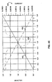
- graphs 400,410,420,430,440,450 are shown illustrating circuit simulation results of the relationship of current in the first, second and third differential transistor pairs 115,120,125 of the circuit 200 to a first input signal 402 and a second input signal 404, which are applied, respectively to the input terminals 105,110.
- the first input signal 402 has a voltage that is equal to a variable voltage 'VA.
- the voltage 'VA' is represented on the x-axis of each of the graphs 400,410,420,430,440.
- the second input signal 404 has a voltage that is equal to '2.0-VA'
- the variable voltage 'VA' is linearly swept from 0 V to 2 V, which results in the first input signal 402 and the second input signal 404 being inverses of one another.
- the actual amplitudes of the first and second input signals 402,404 are shown the left vertical 'Voltage' axis in each Figure. It will be appreciated that the input signals 402 and 404 are merely illustrative to demonstrate the operation of the circuit 200 and any number of forms of input signals may be communicated to the circuit 200 to determine signal coincidence.
- the graph 400 of Figure 4A illustrates the relationship of the currents of the FETs 205 and 210 of the first differential pair 115 of the circuit 200 to the first and second input signals 402,404.
- the current through the FET 205 is represented by the line 408 and the current through the FET 210 is represented by the line 406.
- the magnitude of the currents 406,408 are shown in the right vertical 'Current' axis.
- the currents through the FETs 205,210 are provided by the current source 130, where the sum of those currents 406,408 at any given point in the graph 400 is the tail current of the first differential pair 115.
- the tail current (the sum of the currents 406,408) of the differential pair 115 is constant over the 2.0 V range illustrated.
- the first input signal 402 is applied to a gate terminal of the FET 205 of the first differential pair 115 and the second input signal 404 is applied to the FET 210 of the first differential pair 115.
- VA is 0 V
- the first input signal 402 is also 0 V and the second input signal is 2.0 V.
- the FET 210 is turned on and the FET 205 is turned off. Therefore, the tail current provided by the current source 130 is substantially completely conducted by the FET 210.
- the variable voltage VA is increased, the FET 205 begins to turn on and the FET 210 begins to turn off. This causes the current 406 through the FET 210 to decrease and the current 408 through the FET 205 to increase.
- the current 408 (through the FET 205) is provided to the second differential pair 120 and serves as the tail current for that differential pair.
- the current 406 (through the FET 210) is provided to third differential pair 125 and serves as the tail current for that differential pair.
- the graph 410 of the Figure 4B illustrates the relationship of the currents of the FETs 215 and 220 of the second differential pair 120 of the circuit 200 to the first and second input signals 402,404. It will be appreciated that the currents of the FETs 215,220 are based on the tail current (the current 408 of Figure 4A ) of the second differential pair 120.
- the first input signal 402 is applied to a gate terminal of the FET 220 of the second differential pair 120 and the second input signal 404 is applied to the FET 215 of the second differential pair 120.
- the current 416 is the current through the FET 215 and the current 418 is the through the FET 220.
- the first input signal 402 is also 0 V and the second input signal 404 is 2.0 V.
- the FET 215 is turned on and the FET 220 is turned off.
- the tail current of the second differential pair 120 (the current 408 of Figure 4A ) is also approximately zero. Therefore, the current 416 through the FET 215 is substantially zero in this situation.
- the FET 215 begins to turn off and the FET 220 begins to turn on.
- the tail current (the current 408 of Figure 4A ) of the second differential pair 120 also begins to increase.
- the current 416 through the FET 215 begins to increase in correspondence with the increase in the current 408 but then returns to zero. This occurs because the FET 215 shuts off as the input signal 404 applied to its gate falls below the threshold of the FET 215 as the current 408 continues to increase.
- the current 418 increases in correspondence with the tail current (the current 408) of the second differential pair.
- the current 418 through FET 220 is substantially equivalent to the tail current (the current 408) of the second differential pair 120.
- the graph 420 of the Figure 4C illustrates the relationship of currents 426,428 of the FETs 225 and 230 of the third differential pair 125 to the first and second input signals 402,404. It will be appreciated that the currents 426,428 of the FETs 225,230 are based on the tail current (the current 406 of Figure 4A ) of the third differential pair 125.
- the first input signal 402 is applied to a gate terminal of the FET 230 of the third differential pair 125 and the second input signal 404 is applied to the FET 225 of the third differential pair 125.
- the current 426 is the current through the FET 225 and the current 428 is the current through the FET 230.
- VA is 0 V
- the first input signal 402 is also 0 V
- the second input signal 404 is 2.0 V.
- the FET 225 is turned on and the FET 230 is turned off.
- VA is 0 V
- the tail current of the third differential pair 120 (the current 406 of Figure 4A ) is at its upper value. Therefore, the current 426 through the FET 225 is substantially equivalent to the upper value of the tail current (the current 406) of the third differential pair 125.
- the FET 225 begins to turn off and the FET 230 begins to turn on.
- the tail current (the current 406 of Figure 4A ) of the third differential pair 125 begins to decrease.
- the current 426 through the FET 225 begins to decrease in correspondence to the current 406.
- the current 428 through the FET 230 begins to increase but then returns to zero. This occurs because the tail current (the current 406) of the third differential pair 125 continues to decrease to zero as 'VA' continues to increase.
- the graph 430 in Figure 4D shows a combined current 436 and its relationship to the input signals 402,404.
- the combined current 436 is a combination of the current 416 of the FET 215 and the current 428 of the FET 230.
- the currents 416,428 are combined by coupling the drain terminals of the FETs 215,230 with each other.
- the combined current 436 is communicated to the signal buffer 150 via the current mirrors 140,145 in the fashion described above for use in indicating whether or not the first and second input signals 402,404 are coincident.
- the graph 440 in Figure 4E shows a combined current 446 and its relationship to the input signals 402,404.
- the combined current 446 is a combination of the current 418 of the FET 220 and the current 426 of the FET 225.
- the currents 418,426 are combined by coupling the drain terminals of the FETs 220,225 with each other.
- the combined current 446 is communicated to the signal buffer 150 via the current mirror 135 in the fashion described above for use in indicating whether or not the first and second input signals 402,404 are coincident.
- the current 436 is at (or approaching) its low value and the current 446 is at (or approaching) its upper value. These currents are communicated to the signal buffer 150 (via the current mirrors 135,140,145) to indicate lack of coincidence.
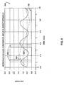
- a graph 500 illustrating the operation of the circuit 200 in detecting coincidence of input signals 502 and 504 is shown.
- the trace 506 is the digital output signal of the circuit 200.
- the signal buffer 150 of the circuit 200 is implemented as an inverter.
- the threshold adjustment device 160 is off (e.g., 0 V is applied to the gate of the FET 280). Therefore, in this situation, the circuit 200 will indicate the coincidence of the input signals 502 and 504 at or above approximately 0 V.
- the pulses 508 of the trace 506 indicate that coincidence of the input signals 502 and 504 has been detected by the circuit 200.
- the width of the pulses 508 indicates the band of coincidence for the circuit 200.
- the width of the pulses 508 varies depending on the relative rate of change of the amplitude of the input signals 502,504 in proximity of actual coincidence of the signals. Actual coincidence may be defined as the voltages of the input signals 502,504 being equal, not just within a coincidence band. If the input signals 502,504 are changing relatively quickly with respect to each other when actual coincidence occurs, the pulse 508 is narrower than if the input signals 502,504 are changing relatively slowly with respect to each when actual coincidence occurs. It will be appreciated that the circuit 200 may indicate that coincidence of the input signals 502 and 504 has occurred without actual coincidence between signals taking place.
- a graph 600 illustrating the operation of the circuit 200 in detecting coincidence of input signals 602 and 604 is shown.
- the trace 606 is the digital output signal of the circuit 200.
- the signal buffer 150 of the circuit 200 is implemented as an inverter.
- the threshold adjustment device 160 is active with a voltage of approximately 1.0V applied to the FET 280. Therefore, in this situation, the circuit 200 will indicate the coincidence of the input signals 602 and 604 at or above approximately 1.0 V.
- the pulses 608 of the trace 606 indicate the coincidence of the input signals 602 and 604 above the threshold voltage of 1.0 V has been detected by the circuit 200. As shown in Figure 6 , coincidence of the input signals 602,604 when the voltage of the signals is below 1.0V (the threshold voltage) does not result in a pulse 608.
Description
- This disclosure relates to signal coincidence detection circuits.
- In analog circuits it is often desirable to determine when two signals are coincident. For purposes of this disclosure, coincidence (or signal coincidence) means that two (or more) voltage signals have substantially the same voltage amplitude at substantially the same point in time. For instance, such (signal) coincidence may be established when the signals being compared are all within a certain range relative to each other (e.g., within a certain percentage or within a certain difference in amplitude). For instance, in a particular embodiment, two signals may be considered to be coincident if they have voltage amplitudes that are within 100 mV of each other. The 100 mV difference may be termed a "coincidence band" or "band of coincidence." In such an embodiment, a voltage signal of 2.9 V would be considered to be coincident with a voltage signal of 2.95 V, while the signal of 2.9 V would not be considered coincident with a voltage signal of 2.85 V. As is known, such signal coincidence may be determined using a signal coincidence detection circuit.
- An example application for such signal coincidence detection circuits is their use to determine "lock" of bandgap reference circuits. Bandgap reference circuits are known and will not be described in detail here. Briefly, however, bandgap reference circuits are used to provide stable voltage references in low-voltage circuits (e.g., ~1.2 V). Additionally, bandgap reference circuits may be used to provide local biases in very large scale integrated circuits. Local biases generated by such bandgap circuits are desirable because they are not substantially affected by ambient noise or transient signals. Bandgap circuits are feedback circuits where a reference signal is applied and a feedback signal is generated based on the reference signal. The bandgap circuit is considered to be "locked" when the feedback signal is coincident (e.g., within a band of coincidence) with the reference signal. As indicated above, such coincidence may be determined using a signal coincidence detection circuit. However, current approaches for implementing such signal coincidence detection circuits have certain drawbacks.
- For instance, current embodiments of signal coincidence detection circuits are fairly complicated analog circuits (e.g., including fifty or more transistors). Such circuits include a series of comparators, where shifts in the threshold of the comparators are used to establish a coincidence band for the signals being compared by the circuit. Such signal coincidence detection circuits also include logic circuitry that is used to determine coincidence between signals of interest (e.g., a reference signal and a feedback signal of a bandgap reference circuit) based on signals that are generated by the series of comparators from the signals of interest. However, because of their complexity, such signal coincidence detection circuits have relatively high power dissipation, may operate slowly and are difficult to design.
- Furthermore, it may be desirable to establish a threshold voltage for coincidence detection (e.g., a voltage level below which coincidence of signals being compared will not be indicated) so that coincidence of the signals being compared that occurs below the threshold voltage is not indicated. In such an approach, additional circuitry is needed for setting such a threshold. Such threshold circuitry thus further increases the design complexity and power dissipation of such circuits. Based on the foregoing, alternative approaches for implementing such signal detection circuits are desirable.
- The foregoing examples of the related art and limitations related therewith are intended to be illustrative and not exclusive. Other limitations of the related art will become apparent to those of skill in the art upon a reading of the specification and a study of the drawings. Other examples of prior art devices can be found disclosed in, for example,
US6605965A andGB2318419A - The following embodiments and aspects thereof are described and illustrated in conjunction with systems, tools and methods which are given by way of example and meant to be illustrative, not limiting in scope. In various embodiments, one or more of the above-described problems have been reduced or eliminated, while other embodiments are directed to other improvements.
- In order to solve the problems associated with the prior art, the present invention provides a signal coincidence detection circuit as defined in claim 1.
- Preferably, the first transistor of the first differential transistor pair is operative to supply the second tail current to the second differential transistor pair; and
the second transistor of the first differential transistor pair is operative to supply the third tail current to the third differential transistor pair. - Preferably, the signal coincidence detection circuit further comprises a current mirror coupled with the second transistor of the second differential transistor pair and the first transistor of the third differential transistor pair, wherein the current mirror is configured to operate as a pull-up device, and wherein the coincidence detection circuit is operative to combine respective currents of the second transistor of the second differential transistor pair and the first transistor of the third differential transistor pair and wherein the current mirror is operative to mirror the combined currents to indicate whether the first and second input signals are coincident to one another.
- Preferably, the signal coincidence detection further comprising a threshold adjustment device coupled with the current mirror, wherein a resistance of the threshold adjustment device is adjustable to establish a voltage threshold below which the signal coincidence circuit will not indicate coincidence of the first and second input signals.
- Preferably, the threshold adjustment device comprises an n-type field effect transistor.
- Preferably, the signal coincidence detection circuit further comprises:
- a first current mirror coupled with the first transistor of the second differential transistor pair and the second transistor of the third differential transistor pair; and
- a second current mirror coupled with the first current mirror, the second current mirror operating as a pull-down device in the signal coincidence detection circuit,
- wherein the signal coincidence detection circuit is configured to combine respective currents of the first transistor of the second differential transistor pair and the second transistor of the third differential transistor pair and the first current mirror is configured to mirror the combined currents; and
- the second current mirror is configured to mirror a current of the first current mirror to indicate whether or not coincidence between the first and second input signals exists.
- Preferably, the signal coincidence detection circuit further comprises:
- a third current mirror coupled with the second transistor of the second differential transistor pair and the first transistor of the third differential transistor pair, the third current mirror operating as a pull-up device in the signal coincidence detection circuit, wherein the signal coincidence detection circuit is configured to combine respective currents of the second transistor of the third differential transistor pair and the first transistor of the second differential transistor pair and the third current mirror is configured to mirror the combined current to indicate whether or not coincidence between the first and second input signals exists; and
- a signal buffer coupled with the second and third current mirrors, wherein, the signal buffer is configured to produce a digital signal based on currents of the second and third current mirrors, the digital signal indicating whether or not coincidence between the first and second input signals exists.
- Preferably, the signal buffer comprises an inverter circuit.
- Preferably, the current source comprises first and second n-type field effect transistors, FETs, wherein:
- a source terminal of the first n-type FET is coupled with electrical ground;
- a drain terminal of the first n-type FET is coupled with a source terminal of the second n-type FET; and
- a drain terminal of the second n-type FET is coupled with respective source terminals of the first and second transistors of the first differential transistor pair.
- Exemplary embodiments are illustrated in referenced figures of the drawings. It is intended that the embodiments and figures disclosed herein are to be considered illustrative rather than restrictive.
-
Figure 1 is a block diagram of a signal coincidence detection circuit with adjustable threshold; -
Figure 2 is a schematic/block diagram illustrating, in further detail, a signal coincidence detection circuit with adjustable threshold; -
Figure 3 is a schematic/block diagram of a cascoded bias generator circuit that may be implemented in the circuits ofFigures 1 and2 ; -
Figures 4A-4E are graphs illustrating voltage and current relationships for the circuit ofFigure 2 ; -
Figure 5 is a graph illustrating signal coincidence detection using the circuit ofFigure 2 with no threshold adjustment; and -
Figure 6 is a graph illustrating signal coincidence detection using the circuit ofFigure 2 with threshold adjustment. - Embodiments of signal coincidence detection circuits and methods that may be implemented by such circuits are shown and described generally herein. As was discussed above, such circuits may be used in any number of applications. It will be appreciated that the particular circuit elements of a specific embodiment will depend, at least in part, on the particular application for which a specific signal coincidence detection circuit is intended.
- Referring to
Figure 1 , a block diagram illustrating an example signalcoincidence detection circuit 100 is shown. Thecircuit 100 includes a firstinput signal terminal 105 and a secondinput signal terminal 110. The input signal terminals 105,110 are coupled with a firstdifferential transistor pair 115, a seconddifferential transistor pair 120 and a thirddifferential transistor pair 125. In operation, the firstinput signal terminal 105 receives a first input signal and the secondinput signal terminal 110 receives a second input signal. The signalcoincidence detection circuit 100 determines whether or not the first and second input signals are coincident. - To determine whether the first and second input signals are coincident, the first and second input signals are communicated from the input signal terminals 105,110 to the first, second and third differential pairs 115,120,125. In comparing the first and second input signals for coincidence, a first tail current is provided to the first
differential pair 115 by acurrent source 130. The firstdifferential pair 115, in turn, provides a second tail current to the second differential transistor pair 120 (e.g., via a first transistor) and a third tail current to the third differential transistor pair 125 (e.g., via a second transistor). The second and third tail currents are based on the first and second input signals. - The second and third differential pairs 120,125 produce a plurality of currents (from the second and third tail currents) based on the first and second input signals. For the
circuit 100, the currents produced by the second and third differential transistor pairs 120,125 are combined to produce two combined currents. To produce the combined currents, respective drain terminals of transistors of the second and third differential transistors pairs 120,125 are coupled to one another, - A first combined current is communicated to a
current mirror 135. Thecurrent mirror 135 operates as a pull-up device in thecircuit 100. A second combined current is communicated to acurrent mirror 140. Thecurrent mirror 140 mirrors the second combined current and communicates that mirrored current to anothercurrent mirror 145. Thecurrent mirror 145 operates as a pull-down device in thecircuit 100. The first and second combined currents are then communicated (via the current mirrors 135,140,145) to asignal buffer 150. - The
signal buffer 150 produces a digital signal based on the first and second combined currents, where the digital signal produced by thesignal buffer 150 indicates whether the first and second input signals are coincident (e.g., within a band of coincidence). For instance, thesignal buffer 150 may generate a logic "1" signal to indicate that the first and second input signals are coincident and generate a logic "0" signal to indicate that the first and second input signals are not coincident. Of course, the opposite may also be the case, where a logic "0" indicates that the input signals are coincident and a logic "1" indicates that the input signals are not coincident. It will be appreciated that, thesignal buffer 150 may take any number of forms. For example, thesignal buffer 150 may be implemented as an inverter or, alternatively, as a hex buffer. The digital signal produced by thesignal buffer 150 may then be communicated to other circuitry via anoutput signal terminal 155. - The signal
coincidence detection circuit 100 further includes athreshold adjustment device 160. Thethreshold adjustment device 160 is coupled with the second and third differential pairs and thecurrent mirror 135. In thecircuit 100, thethreshold adjustment device 160 acts as a current "steering" device. Current is "steered" from the current source 115 (via the differential transistor pairs 115,120,125) by applying a threshold voltage to thethreshold adjustment device 160. - In such an approach, the
threshold adjustment device 160 may take the form of an n-type field effect transistor (FET) that is coupled in parallel with the differential transistor pairs 115,120,125, where a source terminal of the FET is coupled with the current source and a drain terminal of the FET is coupled with the second and third differential pairs and thecurrent mirror 135. Further, the threshold voltage would be applied to a gate terminal of the FET. - In such a circuit, current produced by the current source 130 (and communicated through the differential transistor pairs 115,120,125) would be "steered" through the threshold adjustment device 160 (and away from the current mirror 135) when the first and second input signals have voltage amplitudes that are at or below the threshold voltage applied to the
threshold adjustment device 160. However, for input signals that have voltage amplitudes greater than the applied threshold voltage, only a relatively small portion of the current is "steered" through thethreshold adjustment device 160. The portion of the current that is not "steered" through thethreshold adjustment device 160 is communicated to thecurrent mirror 135 and, in turn, to thesignal buffer 150. This current "steering" results in thecircuit 100 only indicating the coincidence of the first and second input signals when the voltage amplitude of those input signals exceeds the threshold voltage applied to the threshold adjustment device 160 (e.g., the voltage applied to the gate of the n-type FET used to implement the threshold adjustment device 160), - Referring now to
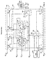
Figure 2 , a schematic diagram illustrating, in more detail, a signalcoincidence detection circuit 200 is shown. Thecircuit 200 includes like elements with thecircuit 100 shown inFigure 1 . The like elements inFigure 2 are referenced with the same reference numbers as the corresponding elements inFigure 1 . For purposes of brevity and clarity, the details of thecircuit 100 that were described above with reference toFigure 1 will not be repeated with reference toFigure 2 except to the extent needed to describe the additional details of thecircuit 200. It will be appreciated, however, that the additional details of thecircuit 200 may also be included in thecircuit 100 but have not been shown inFigure 1 for purposes of clarity. - The
circuit 200 includes apower supply terminal 202 that is used communicate an appropriate power supply voltage to the components of thecircuit 200. Likewise, thecircuit 200 also includes anelectrical ground terminal 204 to provide a ground reference to the components of thecircuit 200. In thecircuit 200, the firstdifferential transistor pair 115 includes a first n-type FET 205 and a second n-type FET 210. The source terminals of the FETs 205,210 are coupled with one another. The seconddifferential pair 120 includes a first n-type FET 215 and a second n-type FET 220, where the source terminals of the FETs 215,220 are coupled with one another. In like fashion, the thirddifferential transistor pair 125 includes a first n-type FET 225 and a second n-type FET 230, where the source terminals of the FETs 225,230 are coupled with one another. - The drain terminal of the
FET 205 of the firstdifferential pair 115 is coupled with the source terminals of the FETs 215,220 of the seconddifferential pair 120 and, as noted above, provides a tail current to the seconddifferential pair 120. In similar fashion, the drain terminal of theFET 210 of the firstdifferential pair 115 is coupled with the source terminals of the FETs 225,230 of the thirddifferential pair 125 and provides a tail current to the thirddifferential pair 125. - As shown in
Figure 2 , the source terminals of the respective FETs of the differential pairs 115,120,125 are coupled directly to one another. In such an embodiment, the band of coincidence (as was discussed above) for thecircuit 200 would be established by adjusting the size of the PETs of the differential pairs 115,120,125. In other embodiments, the coincidence band may also be established using a technique that may be termed resistive degeneration, In such an approach, rather than coupling the source terminals of the respective FETs of each differential pair 115,120,125 directly to each other, resistors are inserted between the source terminals. Such an approach allows for "tuning" of the coincidence band and also increases the linearity of the signal coincidence detection circuit. Resistive degeneration does, however, result in a reduction of the gain of such a signal coincidence detection circuit. Therefore, the particular approach used for establishing a coincidence band will depend on the intended application of a particular signal coincidence detection circuit. - The
current source 130 of thecircuit 200 includes a first n-type FET 235 and a second n-type FET 240 The FETs 235,240 are coupled in a stacked arrangement with the drain of theFET 235 being coupled with the source terminals of theFETs differential pair 115. The source terminal of theFET 235 is coupled with the drain terminal of theFET 240 and the source terminal of theFET 240 is coupled with the electricalground reference terminal 204. The gate terminals of the FETs 235,240 of thecurrent source 130 are coupled with abias generator 245, which provides two direct-current voltage biases to thecurrent source 130. Thecurrent source 130 uses these voltage biases to "mirror" current references provided to thebias generator 245. Thebias generator 245 may take any number of forms. For instance, the bias generator may be implemented as a cascoded bias generator, such as a bias generator is illustrated inFigure 3 and described below. - As shown in
Figure 2 , and as was described above, thesignal buffer 150 may be implemented as aninverter 247. As an alternative, thesignal buffer 150 may be implemented as ahex buffer 249. Other possibilities also exist. For instance, thesignal buffer 150 may be implemented as a series of inverters or hex buffers. It will be appreciated that such an approach may provide additional noise immunity as compared to the use of a single inverter or hex buffer. - In the
circuit 200, drain terminals of thesecond FET 220 of the seconddifferential pair 120 and thefirst FET 225 of the third differential pair are coupled with each other. The drain terminals of the FETs 220,225 are further coupled with thecurrent mirror 135, which acts as a pull-up device in thecircuit 200. Because the drain terminals of the FETs 220,225 are coupled with each other, the currents produced by the FETs 220,225 are combined and communicated to the current mirror 135 (assuming thethreshold adjustment device 160 is off). - The
current mirror 135 includes a first p-type FET 250 and a second p-type FET 255. The combined current from the FETs 220,225 is communicated to theFET 250. The combined current is then mirrored by theFET 255 and the mirrored current is communicated to thesignal buffer 150. - Also in the
circuit 200, drain terminals of thefirst FET 215 of the seconddifferential pair 120 and thesecond FET 230 of the thirddifferential pair 125 are coupled with each other such that the FETs 215,230 produce a second combined current. The second combined current is communicated to thecurrent mirror 140. Thecurrent mirror 140 includes a first p-type FET 260 and a second p-type FET 265. The second combined current is communicated to theFET 260. The second combined current is then mirrored by theFET 265 and communicated to thecurrent mirror 145, which acts as a pull-down device in thecircuit 200. - The
current mirror 145 includes a first n-type FET 270 and a second n-typc FET 275. The mirrored current from thecurrent mirror 140 is communicated to thetransistor 270, which operates as a diode in thecircuit 200. The current is then again mirrored by theFET 275 and communicated to thesignal buffer 150. - The
signal buffer 150 produces a digital signal based on the currents communicated to it by the FETs 255,275. This digital signal indicates whether or not the first and second input signals applied to the input signal terminals 105,110 of thecircuit 200 are coincident. If thesignal buffer 150 in thecircuit 200 is implemented as an inverter, the digital signal produced by thecircuit 200 will be a logic "1" when the first and second input signals are coincident, while the digital signal will be a logic "0'' when the input signals are not coincident. - As shown in
Figure 2 , thethreshold adjustment device 160 is implemented as an n-type FET 280, which acts as a current steering device when establishing a threshold voltage for thecircuit 200. The threshold voltage is applied to a gate terminal of theFET 280 via a thresholdvoltage input terminal 285. When a threshold voltage other than 0 V is applied to the thresholdvoltage input terminal 285, the combined current produced by the FETs 235,240 is "steered" through theFET 280 when the amplitude of the input signals applied to the input signal terminals 105,110 is at or below the threshold voltage, as was discussed above. As was also discussed above, when the amplitude of the input signals is greater than the threshold voltage, only a relatively small portion of the combined current of the FETs 235,240 is "steered" through theFET 280. The remaining portion is communicated to thesignal buffer 150 via thecurrent mirror 135 and used to produce the digital signal to indicate the coincidence of the first and second input signals. -
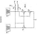
Figure 3 illustrates acascoded bias generator 300 that may be implemented as thebias generator 245 in the signalcoincidence detection circuit 200 ofFigure 2 . Thecascoded bias generator 300, in operation, provides voltage biases to drive the transistors 235,240 of thecurrent source 130 via respective series resistors 330,335 of thebias generator 300. The transistors 235,240 mirror current reference signals provided to thecascoded bias generator 300 by reference current sources 305,310. These voltage biases are communicated to the transistors 235,240 via, respective output terminals 340,345 of thecascoded bias generator 300. - Such cascoded bias generator circuits are known. Therefore, for the purposes of brevity, the operation of such circuits will not be described in detail here. Briefly, however, the
bias generator 300 includes n-type FETs type FETs current source 130 of thecircuit 200, which mirrors the currents provided by the reference current sources 305,310. - Referring to
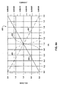
Figures 4A-4E with further reference toFigure 2 , graphs 400,410,420,430,440,450 are shown illustrating circuit simulation results of the relationship of current in the first, second and third differential transistor pairs 115,120,125 of thecircuit 200 to afirst input signal 402 and asecond input signal 404, which are applied, respectively to the input terminals 105,110. - In
Figures 4A-4E , thefirst input signal 402 has a voltage that is equal to a variable voltage 'VA.' The voltage 'VA' is represented on the x-axis of each of the graphs 400,410,420,430,440. Also, in the graphs ofFigures 4A-4E , thesecond input signal 404 has a voltage that is equal to '2.0-VA' For the simulation results shown in the graphs 400,410,410,430,440, the variable voltage 'VA' is linearly swept from 0 V to 2 V, which results in thefirst input signal 402 and thesecond input signal 404 being inverses of one another. The actual amplitudes of the first and second input signals 402,404 are shown the left vertical 'Voltage' axis in each Figure. It will be appreciated that the input signals 402 and 404 are merely illustrative to demonstrate the operation of thecircuit 200 and any number of forms of input signals may be communicated to thecircuit 200 to determine signal coincidence. - The
graph 400 ofFigure 4A illustrates the relationship of the currents of theFETs differential pair 115 of thecircuit 200 to the first and second input signals 402,404. In thegraph 400, the current through theFET 205 is represented by theline 408 and the current through theFET 210 is represented by theline 406. The magnitude of the currents 406,408 are shown in the right vertical 'Current' axis. The currents through the FETs 205,210 are provided by thecurrent source 130, where the sum of those currents 406,408 at any given point in thegraph 400 is the tail current of the firstdifferential pair 115. As shown by thegraph 400, the tail current (the sum of the currents 406,408) of thedifferential pair 115 is constant over the 2.0 V range illustrated. - In the
circuit 200, thefirst input signal 402 is applied to a gate terminal of theFET 205 of the firstdifferential pair 115 and thesecond input signal 404 is applied to theFET 210 of the firstdifferential pair 115. When VA is 0 V, thefirst input signal 402 is also 0 V and the second input signal is 2.0 V. In this situation, theFET 210 is turned on and theFET 205 is turned off. Therefore, the tail current provided by thecurrent source 130 is substantially completely conducted by theFET 210. As the variable voltage VA is increased, theFET 205 begins to turn on and theFET 210 begins to turn off. This causes the current 406 through theFET 210 to decrease and the current 408 through theFET 205 to increase. When VA reaches approximately 1.15 V, the tail current provided by thecurrent source 130 is substantially completely conducted by theFET 215 and the current 406 is approximately zero. As shown inFigure 4A , this transition occurs in the approximate range of VA = 0.85 V - 1.15V. In this range, thefirst input signal 402 and thesecond input signal 404 also cross (have coincidence). The current 408 (through the FET 205) is provided to the seconddifferential pair 120 and serves as the tail current for that differential pair. Likewise, the current 406 (through the FET 210) is provided to thirddifferential pair 125 and serves as the tail current for that differential pair. - The
graph 410 of theFigure 4B illustrates the relationship of the currents of theFETs differential pair 120 of thecircuit 200 to the first and second input signals 402,404. It will be appreciated that the currents of the FETs 215,220 are based on the tail current (the current 408 ofFigure 4A ) of the seconddifferential pair 120. - In the
circuit 200, thefirst input signal 402 is applied to a gate terminal of theFET 220 of the seconddifferential pair 120 and thesecond input signal 404 is applied to theFET 215 of the seconddifferential pair 120. In thegraph 410, the current 416 is the current through theFET 215 and the current 418 is the through theFET 220. For thecircuit 200, when VA is 0 V, thefirst input signal 402 is also 0 V and thesecond input signal 404 is 2.0 V. In this situation, theFET 215 is turned on and theFET 220 is turned off. However, when VA is 0 V, the tail current of the second differential pair 120 (the current 408 ofFigure 4A ) is also approximately zero. Therefore, the current 416 through theFET 215 is substantially zero in this situation. - As the variable voltage 'VA' is increased, the
FET 215 begins to turn off and theFET 220 begins to turn on. Also, the tail current (the current 408 ofFigure 4A ) of the seconddifferential pair 120 also begins to increase. As shown inFigure 4B , the current 416 through theFET 215 begins to increase in correspondence with the increase in the current 408 but then returns to zero. This occurs because theFET 215 shuts off as theinput signal 404 applied to its gate falls below the threshold of theFET 215 as the current 408 continues to increase. - As 'VA' increases causing the
FET 220 to turn on, the current 418 increases in correspondence with the tail current (the current 408) of the second differential pair. Once theFET 215 is "fully" turned off and theFET 220 is "fully" turned on (e.g., when VA reaches approximately 1.1V), the current 418 throughFET 220 is substantially equivalent to the tail current (the current 408) of the seconddifferential pair 120. - The
graph 420 of theFigure 4C illustrates the relationship of currents 426,428 of theFETs differential pair 125 to the first and second input signals 402,404. It will be appreciated that the currents 426,428 of the FETs 225,230 are based on the tail current (the current 406 ofFigure 4A ) of the thirddifferential pair 125. - In the
circuit 200, thefirst input signal 402 is applied to a gate terminal of theFET 230 of the thirddifferential pair 125 and thesecond input signal 404 is applied to theFET 225 of the thirddifferential pair 125. In thegraph 420, the current 426 is the current through theFET 225 and the current 428 is the current through theFET 230. When VA is 0 V, thefirst input signal 402 is also 0 V and thesecond input signal 404 is 2.0 V. In this situation, theFET 225 is turned on and theFET 230 is turned off. Also, when VA is 0 V the tail current of the third differential pair 120 (the current 406 ofFigure 4A ) is at its upper value. Therefore, the current 426 through theFET 225 is substantially equivalent to the upper value of the tail current (the current 406) of the thirddifferential pair 125. - As the variable voltage 'VA' is increased, the
FET 225 begins to turn off and theFET 230 begins to turn on. Also, the tail current (the current 406 ofFigure 4A ) of the thirddifferential pair 125 begins to decrease. As shown inFigure 4C , the current 426 through theFET 225 begins to decrease in correspondence to the current 406. Further, as theFET 230 begins to turn on (around 0.9V), the current 428 through theFET 230 begins to increase but then returns to zero. This occurs because the tail current (the current 406) of the thirddifferential pair 125 continues to decrease to zero as 'VA' continues to increase.. - The
graph 430 inFigure 4D shows a combined current 436 and its relationship to the input signals 402,404. The combined current 436 is a combination of the current 416 of theFET 215 and the current 428 of theFET 230. The currents 416,428 are combined by coupling the drain terminals of the FETs 215,230 with each other. The combined current 436 is communicated to thesignal buffer 150 via the current mirrors 140,145 in the fashion described above for use in indicating whether or not the first and second input signals 402,404 are coincident. - The
graph 440 inFigure 4E shows a combined current 446 and its relationship to the input signals 402,404. The combined current 446 is a combination of the current 418 of theFET 220 and the current 426 of theFET 225. The currents 418,426 are combined by coupling the drain terminals of the FETs 220,225 with each other. The combined current 446 is communicated to thesignal buffer 150 via thecurrent mirror 135 in the fashion described above for use in indicating whether or not the first and second input signals 402,404 are coincident. - As shown in
Figures 4D and4E , when thefirst input signal 402 and thesecond input signal 404 are coincident, the combined current 436 is at an upper value and the combined current 446 is at a low value. These currents are communicated to the signal buffer 150 (via the current mirrors 135,140,145) to indicate coincidence. The width of the vertical portion of the traces representing the currents 436,446 around the coincidence of the input signals 402,404 (e.g., in the range of VA = 0.9V to 1.1V) corresponds with the coincidence band for thecircuit 200. The exact range of the coincidence band will depend on the particular embodiment. - For values of 'VA' outside the coincidence band, the current 436 is at (or approaching) its low value and the current 446 is at (or approaching) its upper value. These currents are communicated to the signal buffer 150 (via the current mirrors 135,140,145) to indicate lack of coincidence.
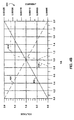
- Referring now to
Figure 5 , agraph 500 illustrating the operation of thecircuit 200 in detecting coincidence of input signals 502 and 504 is shown. In thegraph 500, thetrace 506 is the digital output signal of thecircuit 200. For this particular example, thesignal buffer 150 of thecircuit 200 is implemented as an inverter. Also in this example, thethreshold adjustment device 160 is off (e.g., 0 V is applied to the gate of the FET 280). Therefore, in this situation, thecircuit 200 will indicate the coincidence of the input signals 502 and 504 at or above approximately 0 V. - In the
graph 500, thepulses 508 of thetrace 506 indicate that coincidence of the input signals 502 and 504 has been detected by thecircuit 200. The width of thepulses 508 indicates the band of coincidence for thecircuit 200. As shown inFigure 5 , the width of thepulses 508 varies depending on the relative rate of change of the amplitude of the input signals 502,504 in proximity of actual coincidence of the signals. Actual coincidence may be defined as the voltages of the input signals 502,504 being equal, not just within a coincidence band. If the input signals 502,504 are changing relatively quickly with respect to each other when actual coincidence occurs, thepulse 508 is narrower than if the input signals 502,504 are changing relatively slowly with respect to each when actual coincidence occurs. It will be appreciated that thecircuit 200 may indicate that coincidence of the input signals 502 and 504 has occurred without actual coincidence between signals taking place. - Referring now to
Figure 6 , agraph 600 illustrating the operation of thecircuit 200 in detecting coincidence of input signals 602 and 604 is shown. In thegraph 600, thetrace 606 is the digital output signal of thecircuit 200. For this particular example, as with thegraph 500 ofFigure 5 , thesignal buffer 150 of thecircuit 200 is implemented as an inverter. Also in this example, thethreshold adjustment device 160 is active with a voltage of approximately 1.0V applied to theFET 280. Therefore, in this situation, thecircuit 200 will indicate the coincidence of the input signals 602 and 604 at or above approximately 1.0 V. - In the
graph 600, thepulses 608 of thetrace 606 indicate the coincidence of the input signals 602 and 604 above the threshold voltage of 1.0 V has been detected by thecircuit 200. As shown inFigure 6 , coincidence of the input signals 602,604 when the voltage of the signals is below 1.0V (the threshold voltage) does not result in apulse 608.
Claims (9)
- A signal coincidence detection circuit (100, 200) comprising:a first differential transistor pair (115);a second differential transistor pair (120) coupled with the first differential transistor pair (115); a third differential transistor pair (125) coupled with the first differential transistor pair (115) in parallel with the second differential transistor pair (120), wherein a gate terminal of a first transistor (225) of the third differential transistor pair (125) is coupled to a gate terminal of a first transistor (215) of the second transistor pair (120), and wherein a gate terminal of a second transistor (235) of the third transistor pair (125) is coupled to a gate terminal of a second transistor (220) of the second transistor pair (120);the first differential transistor pair (115) being coupled with the third differential and second differential transistor pairs, wherein a second transistor (210) of the first transistor pair (115) is coupled to the first and second transistors of the third transistor pair (125) and wherein a first transistor (205) of the first transistor pair (115) is coupled to the first and second transistors of the second transistor pair (120); characterised bya first input signal terminal (105) directly coupled with the gate terminal of the first transistor (205) of the first transistor pair, the gate terminal of the second transistor (220) of the second transistor pair and a gate terminal of the second transistor (230) of the third transistor pair, wherein the first input signal terminal is configured to receive a first input signal and communicate the first input signal to the first, second and third differential transistor pairs;a second input signal terminal (110) directly coupled with the gate terminal of the second transistor (210) of the first transistor pair, the gate terminal of the first transistor (215) of the second transistor pair, and a gate terminal of the first transistor (225) of the third transistor pair, wherein the second input signal terminal is configured to receive a second input signal and communicate the second input signal to the first, second and third differential transistor pairs;a current source (130) coupled with the first differential transistor pair and configured to supply a first tail current to the first transistor pair, wherein the first transistor pair is configured to provide a second tail current to the second transistor pair, and a third tail current to the third transistor pair, wherein the second and third tail currents are based on the first input signal received at the first input signal terminal and the second input signal received at the second input signal terminal; andwherein, the signal coincidence detection circuit is configured to combine currents of the second and third differential transistor pairs to produce at least one combined current, wherein the at least one combined current indicates whether or not the first and second input signals are coincident with one another.
- The signal coincidence detection circuit (100, 200) of claim 1, wherein
the first transistor (205) of the first differential transistor pair (115) is operative to supply the second tail current to the second differential transistor pair (120) ; and
the second transistor (210) of the first differential transistor pair is operative to supply the third tail current to the third differential transistor pair (125). - The signal coincidence detection circuit (100, 200) of claim 2, further comprising a current mirror (135) coupled with the second transistor (220) of the second differential transistor pair (120) and the first transistor (225) of the third differential transistor pair (125), wherein the current mirror is configured to operate as a pull-up device, and wherein the coincidence detection circuit is operative to combine respective currents of the second transistor of the second differential transistor pair and the first transistor of the third differential transistor pair and wherein the current mirror is operative to mirror the combined currents to indicate whether the first and second input signals are coincident to one another.
- The signal coincidence detection circuit (100, 200) of claim 3, further comprising a threshold adjustment device (160) coupled with the current mirror (135), wherein a resistance of the threshold adjustment device is adjustable to establish a voltage threshold below which the signal coincidence circuit will not indicate coincidence of the first and second input signals.
- The signal coincidence detection circuit of claim 4, wherein the threshold adjustment device (160) comprises an n-type field effect transistor (280).
- The signal coincidence detection circuit of claim 2, further comprising:a first current mirror (140) coupled with the first transistor (215) of the second differential transistor pair (120) and the second transistor (230) of the third differential transistor pair (125); anda second current mirror (145) coupled with the first current mirror, the second current mirror operating as a pull-down device in the signal coincidence detection circuit,wherein the signal coincidence detection circuit is configured to combine respective currents of the first transistor of the second differential transistor pair and the second transistor of the third differential transistor pair and the first current mirror is configured to mirror the combined currents; andthe second current mirror is configured to mirror a current of the first current mirror to indicate whether or not coincidence between the first and second input signals exists.
- The signal coincidence detection circuit (100, 200) of claim 6, further comprising:a third current mirror (135) coupled with the second transistor (220) of the second differential transistor pair (120) and the first transistor (225) of the third differential transistor pair (125), the third current mirror operating as a pull-up device in the signal coincidence detection circuit, wherein the signal coincidence detection circuit is configured to combine respective currents of the second transistor of the second differential transistor pair and the first transistor of the third differential transistor pair and the third current mirror is configured to mirror the combined current to indicate whether or not coincidence between the first and second input signals exists; anda signal buffer (150) coupled with the second and third current mirrors, wherein, the signal buffer is configured to produce a digital signal based on currents of the second and third current mirrors, the digital signal indicating whether or not coincidence between the first and second input signals exists.
- The signal coincidence detection circuit (100, 200) of claim 7, wherein the signal buffer (150) comprises an inverter circuit.
- The signal coincidence detection circuit (100, 200) of claim 1, wherein the current source (130) comprises first (240) and second (235) n-type field effect transistors, FETs, wherein:a source terminal of the first n-type FET is coupled with electrical ground (204);a drain terminal of the first n-type FET is coupled with a source terminal of the second n-type FET; anda drain terminal of the second n-type FET is coupled with respective source terminals of the first (205) and second (210) transistors of the first differential transistor pair (115).
Applications Claiming Priority (1)
| Application Number | Priority Date | Filing Date | Title |
|---|---|---|---|
| US11/408,870 US7279909B1 (en) | 2006-04-20 | 2006-04-20 | Signal coincidence detection circuit |
Publications (3)
| Publication Number | Publication Date |
|---|---|
| EP1847902A2 EP1847902A2 (en) | 2007-10-24 |
| EP1847902A3 EP1847902A3 (en) | 2009-01-21 |
| EP1847902B1 true EP1847902B1 (en) | 2012-06-06 |
Family
ID=38441442
Family Applications (1)
| Application Number | Title | Priority Date | Filing Date |
|---|---|---|---|
| EP07106477A Expired - Fee Related EP1847902B1 (en) | 2006-04-20 | 2007-04-19 | Signal coincidence detection circuit |
Country Status (3)
| Country | Link |
|---|---|
| US (1) | US7279909B1 (en) |
| EP (1) | EP1847902B1 (en) |
| JP (1) | JP5148158B2 (en) |
Families Citing this family (2)
| Publication number | Priority date | Publication date | Assignee | Title |
|---|---|---|---|---|
| US8283956B2 (en) * | 2009-04-01 | 2012-10-09 | Honeywell International Inc. | Radiation-hardened charge pump topology |
| US9891642B2 (en) * | 2015-07-02 | 2018-02-13 | Novatek Microelectronics Corp. | Current source and current supply system with hysteresis |
Family Cites Families (14)
| Publication number | Priority date | Publication date | Assignee | Title |
|---|---|---|---|---|
| DE2213062B2 (en) * | 1972-03-17 | 1980-09-25 | Siemens Ag, 1000 Berlin Und 8000 Muenchen | Trigger circuit with transistors as emitter resistors - uses inverting differential amplifier to increase precision of opposing phases |
| US4061932A (en) * | 1976-02-17 | 1977-12-06 | Bell Telephone Laboratories, Incorporated | Window comparator |
| JPS5775022A (en) * | 1980-10-29 | 1982-05-11 | Nec Corp | Comparator |
| EP0111230B1 (en) * | 1982-11-26 | 1987-03-11 | Nec Corporation | Voltage comparator circuit |
| JPS6387014A (en) * | 1986-09-30 | 1988-04-18 | Sony Corp | Latched comparator |
| JPH1013210A (en) * | 1996-03-12 | 1998-01-16 | Lsi Logic Corp | Differential-cmos level converter, provided with cross voltage adjusting function |
| JP3092529B2 (en) * | 1996-10-18 | 2000-09-25 | 日本電気株式会社 | Window comparator circuit |
| JP3920427B2 (en) * | 1997-11-19 | 2007-05-30 | 富士通株式会社 | Differential amplifier circuit and operational amplifier circuit |
| US6252434B1 (en) * | 1999-02-04 | 2001-06-26 | Motorola, Inc. | Voltage comparator |
| JP2000323967A (en) * | 1999-05-10 | 2000-11-24 | Matsushita Electric Ind Co Ltd | Hysteresis circuit |
| JP2001177380A (en) * | 1999-12-17 | 2001-06-29 | Yokogawa Electric Corp | Comparator circuit and oscillation circuit using the same |
| JP2001267896A (en) * | 2000-03-17 | 2001-09-28 | Nec Corp | Voltage comparator |
| US6605965B1 (en) * | 2001-09-26 | 2003-08-12 | Micrel, Incorporated | Differential window comparator |
| JP2004304564A (en) * | 2003-03-31 | 2004-10-28 | Kawasaki Microelectronics Kk | Fluctuation compensating oscillator |
-
2006
- 2006-04-20 US US11/408,870 patent/US7279909B1/en active Active
-
2007
- 2007-04-19 EP EP07106477A patent/EP1847902B1/en not_active Expired - Fee Related
- 2007-04-20 JP JP2007111232A patent/JP5148158B2/en not_active Expired - Fee Related
Also Published As
| Publication number | Publication date |
|---|---|
| EP1847902A3 (en) | 2009-01-21 |
| US20070247174A1 (en) | 2007-10-25 |
| US7279909B1 (en) | 2007-10-09 |
| JP2007295570A (en) | 2007-11-08 |
| JP5148158B2 (en) | 2013-02-20 |
| EP1847902A2 (en) | 2007-10-24 |
Similar Documents
| Publication | Publication Date | Title |
|---|---|---|
| US10536309B2 (en) | Demodulation of on-off-key modulated signals in signal isolator systems | |
| US7940036B2 (en) | Voltage comparison circuit, and semiconductor integrated circuit and electronic device having the same | |
| US7924085B2 (en) | Negative analog switch design | |
| US20040189386A1 (en) | Differential amplifier operable in wide range | |
| US7728632B1 (en) | Integrated circuit comparators having improved input resolution and methods of operating same | |
| US8803535B2 (en) | Impedance mismatch detection circuit | |
| EP1908168B1 (en) | Temperature-independent amplifier offset trim circuit | |
| US20060170462A1 (en) | Reliability comparator with hysteresis | |
| US8405439B2 (en) | Duty cycle adjusting system | |
| US9083262B2 (en) | Voltage mode driver with current booster (VMDCB) | |
| US8436661B2 (en) | Input buffer capable of expanding an input level range | |
| US9628076B2 (en) | Transmission circuit and semiconductor integrated circuit | |
| US7511553B2 (en) | Current controlled level shifter with signal feedback | |
| US20080238521A1 (en) | Low differential output voltage circuit | |
| CN103684279A (en) | Circuits for improving linearity of metal oxide semiconductor (MOS) transistors | |
| CN109690937B (en) | Selectable current limiter circuit | |
| US6759878B2 (en) | Voltage comparator circuit and substrate bias adjusting circuit using same | |
| EP1847902B1 (en) | Signal coincidence detection circuit | |
| US8988106B2 (en) | Voltage mode driver with current booster (VMDCB) | |
| US7474133B1 (en) | Apparatus and method for high-speed serial communications | |
| EP2876812B1 (en) | Input circuit with mirroring | |
| EP1550149B1 (en) | Constant delay zero standby differential logic receiver and method | |
| US6275082B1 (en) | Receiver with switched current feedback for controlled hysteresis | |
| US11228466B2 (en) | Digital capacitive isolator | |
| JP2007097131A (en) | Differential amplifier |
Legal Events
| Date | Code | Title | Description |
|---|---|---|---|
| PUAI | Public reference made under article 153(3) epc to a published international application that has entered the european phase |
Free format text: ORIGINAL CODE: 0009012 |
|
| AK | Designated contracting states |
Kind code of ref document: A2 Designated state(s): AT BE BG CH CY CZ DE DK EE ES FI FR GB GR HU IE IS IT LI LT LU LV MC MT NL PL PT RO SE SI SK TR |
|
| AX | Request for extension of the european patent |
Extension state: AL BA HR MK YU |
|
| PUAL | Search report despatched |
Free format text: ORIGINAL CODE: 0009013 |
|
| AK | Designated contracting states |
Kind code of ref document: A3 Designated state(s): AT BE BG CH CY CZ DE DK EE ES FI FR GB GR HU IE IS IT LI LT LU LV MC MT NL PL PT RO SE SI SK TR |
|
| AX | Request for extension of the european patent |
Extension state: AL BA HR MK RS |
|
| 17P | Request for examination filed |
Effective date: 20090710 |
|
| 17Q | First examination report despatched |
Effective date: 20090806 |
|
| AKX | Designation fees paid |
Designated state(s): DE FR GB |
|
| GRAP | Despatch of communication of intention to grant a patent |
Free format text: ORIGINAL CODE: EPIDOSNIGR1 |
|
| GRAS | Grant fee paid |
Free format text: ORIGINAL CODE: EPIDOSNIGR3 |
|
| GRAA | (expected) grant |
Free format text: ORIGINAL CODE: 0009210 |
|
| AK | Designated contracting states |
Kind code of ref document: B1 Designated state(s): DE FR GB |
|
| REG | Reference to a national code |
Ref country code: GB Ref legal event code: FG4D |
|
| REG | Reference to a national code |
Ref country code: DE Ref legal event code: R096 Ref document number: 602007023116 Country of ref document: DE Effective date: 20120802 |
|
| PLBE | No opposition filed within time limit |
Free format text: ORIGINAL CODE: 0009261 |
|
| STAA | Information on the status of an ep patent application or granted ep patent |
Free format text: STATUS: NO OPPOSITION FILED WITHIN TIME LIMIT |
|
| 26N | No opposition filed |
Effective date: 20130307 |
|
| REG | Reference to a national code |
Ref country code: DE Ref legal event code: R097 Ref document number: 602007023116 Country of ref document: DE Effective date: 20130307 |
|
| REG | Reference to a national code |
Ref country code: FR Ref legal event code: PLFP Year of fee payment: 10 |
|
| REG | Reference to a national code |
Ref country code: FR Ref legal event code: PLFP Year of fee payment: 11 |
|
| REG | Reference to a national code |
Ref country code: FR Ref legal event code: PLFP Year of fee payment: 12 |
|
| PGFP | Annual fee paid to national office [announced via postgrant information from national office to epo] |
Ref country code: DE Payment date: 20210428 Year of fee payment: 15 Ref country code: FR Payment date: 20210427 Year of fee payment: 15 |
|
| PGFP | Annual fee paid to national office [announced via postgrant information from national office to epo] |
Ref country code: GB Payment date: 20210426 Year of fee payment: 15 |
|
| REG | Reference to a national code |
Ref country code: DE Ref legal event code: R119 Ref document number: 602007023116 Country of ref document: DE |
|
| GBPC | Gb: european patent ceased through non-payment of renewal fee |
Effective date: 20220419 |
|
| PG25 | Lapsed in a contracting state [announced via postgrant information from national office to epo] |
Ref country code: GB Free format text: LAPSE BECAUSE OF NON-PAYMENT OF DUE FEES Effective date: 20220419 Ref country code: FR Free format text: LAPSE BECAUSE OF NON-PAYMENT OF DUE FEES Effective date: 20220430 Ref country code: DE Free format text: LAPSE BECAUSE OF NON-PAYMENT OF DUE FEES Effective date: 20221103 |
|
| P01 | Opt-out of the competence of the unified patent court (upc) registered |
Effective date: 20230525 |