EP1845556A1 - Electric component mounting apparatus - Google Patents
Electric component mounting apparatus Download PDFInfo
- Publication number
- EP1845556A1 EP1845556A1 EP06712384A EP06712384A EP1845556A1 EP 1845556 A1 EP1845556 A1 EP 1845556A1 EP 06712384 A EP06712384 A EP 06712384A EP 06712384 A EP06712384 A EP 06712384A EP 1845556 A1 EP1845556 A1 EP 1845556A1
- Authority
- EP
- European Patent Office
- Prior art keywords
- pressing force
- pressure bonding
- force adjusting
- bonding member
- mounting device
- Prior art date
- Legal status (The legal status is an assumption and is not a legal conclusion. Google has not performed a legal analysis and makes no representation as to the accuracy of the status listed.)
- Withdrawn
Links
Images


Classifications
-
- H—ELECTRICITY
- H10—SEMICONDUCTOR DEVICES; ELECTRIC SOLID-STATE DEVICES NOT OTHERWISE PROVIDED FOR
- H10P—GENERIC PROCESSES OR APPARATUS FOR THE MANUFACTURE OR TREATMENT OF DEVICES COVERED BY CLASS H10
- H10P72/00—Handling or holding of wafers, substrates or devices during manufacture or treatment thereof
- H10P72/70—Handling or holding of wafers, substrates or devices during manufacture or treatment thereof for supporting or gripping
- H10P72/74—Handling or holding of wafers, substrates or devices during manufacture or treatment thereof for supporting or gripping using temporarily an auxiliary support
-
- H—ELECTRICITY
- H05—ELECTRIC TECHNIQUES NOT OTHERWISE PROVIDED FOR
- H05K—PRINTED CIRCUITS; CASINGS OR CONSTRUCTIONAL DETAILS OF ELECTRIC APPARATUS; MANUFACTURE OF ASSEMBLAGES OF ELECTRICAL COMPONENTS
- H05K13/00—Apparatus or processes specially adapted for manufacturing or adjusting assemblages of electric components
- H05K13/04—Mounting of components, e.g. of leadless components
-
- B—PERFORMING OPERATIONS; TRANSPORTING
- B30—PRESSES
- B30B—PRESSES IN GENERAL
- B30B15/00—Details of, or accessories for, presses; Auxiliary measures in connection with pressing
- B30B15/02—Dies; Inserts therefor; Mounting thereof; Moulds
- B30B15/022—Moulds for compacting material in powder, granular of pasta form
- B30B15/024—Moulds for compacting material in powder, granular of pasta form using elastic mould parts
-
- B—PERFORMING OPERATIONS; TRANSPORTING
- B30—PRESSES
- B30B—PRESSES IN GENERAL
- B30B15/00—Details of, or accessories for, presses; Auxiliary measures in connection with pressing
- B30B15/06—Platens or press rams
- B30B15/065—Press rams
-
- B—PERFORMING OPERATIONS; TRANSPORTING
- B30—PRESSES
- B30B—PRESSES IN GENERAL
- B30B5/00—Presses characterised by the use of pressing means other than those mentioned in the preceding groups
- B30B5/02—Presses characterised by the use of pressing means other than those mentioned in the preceding groups wherein the pressing means is in the form of a flexible element, e.g. diaphragm, urged by fluid pressure
-
- H—ELECTRICITY
- H05—ELECTRIC TECHNIQUES NOT OTHERWISE PROVIDED FOR
- H05K—PRINTED CIRCUITS; CASINGS OR CONSTRUCTIONAL DETAILS OF ELECTRIC APPARATUS; MANUFACTURE OF ASSEMBLAGES OF ELECTRICAL COMPONENTS
- H05K3/00—Apparatus or processes for manufacturing printed circuits
- H05K3/30—Assembling printed circuits with electric components, e.g. with resistors
- H05K3/32—Assembling printed circuits with electric components, e.g. with resistors electrically connecting electric components or wires to printed circuits
-
- H—ELECTRICITY
- H10—SEMICONDUCTOR DEVICES; ELECTRIC SOLID-STATE DEVICES NOT OTHERWISE PROVIDED FOR
- H10W—GENERIC PACKAGES, INTERCONNECTIONS, CONNECTORS OR OTHER CONSTRUCTIONAL DETAILS OF DEVICES COVERED BY CLASS H10
- H10W72/00—Interconnections or connectors in packages
- H10W72/01—Manufacture or treatment
- H10W72/0198—Manufacture or treatment batch processes
-
- H—ELECTRICITY
- H10—SEMICONDUCTOR DEVICES; ELECTRIC SOLID-STATE DEVICES NOT OTHERWISE PROVIDED FOR
- H10W—GENERIC PACKAGES, INTERCONNECTIONS, CONNECTORS OR OTHER CONSTRUCTIONAL DETAILS OF DEVICES COVERED BY CLASS H10
- H10W72/00—Interconnections or connectors in packages
- H10W72/071—Connecting or disconnecting
- H10W72/0711—Apparatus therefor
-
- H—ELECTRICITY
- H10—SEMICONDUCTOR DEVICES; ELECTRIC SOLID-STATE DEVICES NOT OTHERWISE PROVIDED FOR
- H10W—GENERIC PACKAGES, INTERCONNECTIONS, CONNECTORS OR OTHER CONSTRUCTIONAL DETAILS OF DEVICES COVERED BY CLASS H10
- H10W72/00—Interconnections or connectors in packages
- H10W72/071—Connecting or disconnecting
- H10W72/0711—Apparatus therefor
- H10W72/07141—Means for applying energy, e.g. ovens or lasers
-
- H—ELECTRICITY
- H10—SEMICONDUCTOR DEVICES; ELECTRIC SOLID-STATE DEVICES NOT OTHERWISE PROVIDED FOR
- H10W—GENERIC PACKAGES, INTERCONNECTIONS, CONNECTORS OR OTHER CONSTRUCTIONAL DETAILS OF DEVICES COVERED BY CLASS H10
- H10W72/00—Interconnections or connectors in packages
- H10W72/071—Connecting or disconnecting
- H10W72/073—Connecting or disconnecting of die-attach connectors
-
- H—ELECTRICITY
- H10—SEMICONDUCTOR DEVICES; ELECTRIC SOLID-STATE DEVICES NOT OTHERWISE PROVIDED FOR
- H10W—GENERIC PACKAGES, INTERCONNECTIONS, CONNECTORS OR OTHER CONSTRUCTIONAL DETAILS OF DEVICES COVERED BY CLASS H10
- H10W72/00—Interconnections or connectors in packages
- H10W72/071—Connecting or disconnecting
- H10W72/073—Connecting or disconnecting of die-attach connectors
- H10W72/07331—Connecting techniques
-
- H—ELECTRICITY
- H10—SEMICONDUCTOR DEVICES; ELECTRIC SOLID-STATE DEVICES NOT OTHERWISE PROVIDED FOR
- H10W—GENERIC PACKAGES, INTERCONNECTIONS, CONNECTORS OR OTHER CONSTRUCTIONAL DETAILS OF DEVICES COVERED BY CLASS H10
- H10W72/00—Interconnections or connectors in packages
- H10W72/30—Die-attach connectors
- H10W72/321—Structures or relative sizes of die-attach connectors
- H10W72/325—Die-attach connectors having a filler embedded in a matrix
-
- H—ELECTRICITY
- H10—SEMICONDUCTOR DEVICES; ELECTRIC SOLID-STATE DEVICES NOT OTHERWISE PROVIDED FOR
- H10W—GENERIC PACKAGES, INTERCONNECTIONS, CONNECTORS OR OTHER CONSTRUCTIONAL DETAILS OF DEVICES COVERED BY CLASS H10
- H10W72/00—Interconnections or connectors in packages
- H10W72/30—Die-attach connectors
- H10W72/351—Materials of die-attach connectors
-
- H—ELECTRICITY
- H10—SEMICONDUCTOR DEVICES; ELECTRIC SOLID-STATE DEVICES NOT OTHERWISE PROVIDED FOR
- H10W—GENERIC PACKAGES, INTERCONNECTIONS, CONNECTORS OR OTHER CONSTRUCTIONAL DETAILS OF DEVICES COVERED BY CLASS H10
- H10W74/00—Encapsulations, e.g. protective coatings
- H10W74/10—Encapsulations, e.g. protective coatings characterised by their shape or disposition
- H10W74/15—Encapsulations, e.g. protective coatings characterised by their shape or disposition on active surfaces of flip-chip devices, e.g. underfills
-
- H—ELECTRICITY
- H10—SEMICONDUCTOR DEVICES; ELECTRIC SOLID-STATE DEVICES NOT OTHERWISE PROVIDED FOR
- H10W—GENERIC PACKAGES, INTERCONNECTIONS, CONNECTORS OR OTHER CONSTRUCTIONAL DETAILS OF DEVICES COVERED BY CLASS H10
- H10W90/00—Package configurations
- H10W90/701—Package configurations characterised by the relative positions of pads or connectors relative to package parts
- H10W90/721—Package configurations characterised by the relative positions of pads or connectors relative to package parts of bump connectors
- H10W90/724—Package configurations characterised by the relative positions of pads or connectors relative to package parts of bump connectors between a chip and a stacked insulating package substrate, interposer or RDL
-
- H—ELECTRICITY
- H10—SEMICONDUCTOR DEVICES; ELECTRIC SOLID-STATE DEVICES NOT OTHERWISE PROVIDED FOR
- H10W—GENERIC PACKAGES, INTERCONNECTIONS, CONNECTORS OR OTHER CONSTRUCTIONAL DETAILS OF DEVICES COVERED BY CLASS H10
- H10W90/00—Package configurations
- H10W90/701—Package configurations characterised by the relative positions of pads or connectors relative to package parts
- H10W90/731—Package configurations characterised by the relative positions of pads or connectors relative to package parts of die-attach connectors
- H10W90/734—Package configurations characterised by the relative positions of pads or connectors relative to package parts of die-attach connectors between a chip and a stacked insulating package substrate, interposer or RDL
Definitions
- the present invention relates to techniques for mounting electrical components, for example, semiconductor chips or the like on a wiring board, and particularly, to techniques for mounting electrical components using an adhesive agent.
- thermocompression bonding of IC chips using a thermocompression bonding head made of an elastic body such as silicone rubber for example, see Patent Documents 1 and 2.
- thermocompression bonding head made of an elastic body
- Patent document 1 JP 2000-79611A
- Patent document 2 JP 2002-359264A
- the present invention has been achieved to solve such problems of conventional techniques, and it is an object of the present invention to provide a mounting device that can mount a plurality of electrical components with an adhesive agent in a highly reliable manner.
- the present invention for achieving the above-described purpose provides a mounting device for an electric component that includes a thermocompression bonding head that includes a pressure bonding member made of a predetermined elastomer that is provided in a head main body, and a pressing force adjusting mechanism for adjusting a pressing force corresponding to a region on a pressure bonding surface of the pressure bonding member, wherein the pressure bonding member is pressed at a predetermined pressure towards an electric component placed on a wiring board.
- the present invention provides the mounting device described above, wherein a plurality of frame-shaped pressing force adjusting portions are provided in the head main body as the pressing force adjusting mechanism, and the pressure bonding member is disposed inside the pressing force adjusting portions.
- the present invention provides the mounting device described above, wherein a pressing force adjusting portion in the form of a protrusion is provided in the head main body as the pressing force adjusting mechanism.
- the present invention provides the mounting device described above, wherein the heights of the pressing force adjusting portions are differentiated.
- the present invention provides the mounting device described above, wherein the pressing force adjusting mechanism is buried in the pressure bonding member.
- the present invention provides the mounting device described above, wherein the pressing force adjusting mechanism includes a cut portion in the pressure bonding member.
- the present invention provides the mounting device described above, wherein the pressing force adjusting mechanism comprises a plurality of the pressure bonding members integrally connected.
- the present invention provides the mounting device described above that includes a base for supporting the wiring board, and a heater provided in the base.
- an electrical component when an electrical component is pressed by a pressure bonding member made of a predetermined elastomer during thermocompression bonding, while a region on the pressed side of the electrical component (for example, a top region opposing the pressure bonding member) is pressed at a predetermined pressure toward the wiring board, a region on the lateral sides of the electrical component is pressed at a smaller pressure than the pressure applied to the region on the pressed side.
- connection of IC chips, etc. can be performed in a highly reliable manner using an anisotropic conductive adhesive film, for example.
- a pressing force adjusting mechanism for adjusting the pressing force for each of various regions on a pressure bonding surface of the pressure bonding member is provided, and such that when pressing a plurality of electrical components simultaneously with respective pressure bonding portions, it is possible to press regions on the pressed side and the lateral sides of each electrical component respectively with an optimal force. This result in highly reliable mounting and avoids displacement between each electrical component and the board during the pressure bonding.
- a plurality of frame-shaped pressing force adjusting portions as the pressing force adjusting mechanism are provided in the head main body.
- the pressure bonding member is arranged inside these pressing force adjusting frame portions, it becomes possible to achieve without fail a condition with respect to a corresponding electrical component that regions on the lateral sides of an electrical component are pressed with a smaller pressure than regions on the pressed side of the electrical component.
- fine adjustment of the materials, hardness degree, and other properties of the pressure bonding member in the pressing force adjusting frame portions is possbile, displacement can be reliably prevented when a large number of electrical components are mounted at simultaneously.
- a pressing force adjusting portion in the form of protrusion is provided in the head main body as the pressing force adjusting mechanism, and/or the pressing force adjusting portions are configured such that the heights of the pressing force adjusting portions are differentiated, the pressing force applied to each of various regions on the pressure bonding surface of the pressure bonding member can be optimazed. Consequently it is possible to perform more reliable thermocompression bonding for a plurality of electrical components simultaneously by avoiding positional displacement of the electrical components.
- thermocompression bonding head based on the number, allocation position, size or the like of the electrical component, and thermocompression bonding can be performed for a plurality of electrical components of various types simultaneously, without the disadvantage of positional displacement of the various electrical components.
- a cut portion is provided in the pressure bonding member as the pressing force adjusting mechanism such that only the portion of the pressure bonding member contacting the electrical component is compressed without the pressing force being transmitted to adjacent portions beyond the cut portion. Consequently, it becomes possible to prevent positional displacement of the electrical component by a simple method without forming a frame portion.
- the pressing force adjusting mechanism comprises a plurality of pressure bonding members integrally formed
- the gap similar to the cut portion described above can be formed in the pressure bonding member, so as to prevent positional displacement of the electrical component by a simple method without use of a frame portion.
- a plurality of electrical components can be mounted with an adhesive agent with a high degree of reliability.
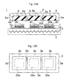
- Fig. 1(a) is a schematic construction diagram showing major portions of a mounting device of the present embodiment
- Fig. 1(b) is an explanatory diagram illustrating the positional relationship between a thermocompression bonding head of the mounting device and IC chips.
- a mounting device 1 includes a base 2 that holds a wiring board 10 on which a wiring pattern 10a is formed, and a thermocompression bonding head 4 for applying pressure and heat to an IC chip (electrical component) 20 having a bump 20b.
- the base 2 is made of a predetermined metal and a heater 3 for heating is provided inside the base 2.
- the thermocompression bonding head 4 includes a head main body 5 made of a predetermined metal, and a heater (not shown) for heating is provided inside thereof.
- a plurality of pressing force adjusting frames (pressing force adjusting mechanism) 5a are provided so as to correspond to a plurality of IC chips 20.
- Concave portions 5b are provided that are divided into plural spaces by the pressing force adjusting frames 5a.
- a pressure bonding members 6 made of a plate-shaped elastomer is attached to the inner wall of each of the concave portions 5b.
- the pressure bonding member 6 of the present embodiment is disposed such that a flat pressure bonding surface 6a is in a substantially horizontal position.
- the pressure bonding surface 6a of the pressure bonding member 6 is configured to have a larger area than the area of a top portion 20a of the IC chip 20 so as to apply uniform force to the top portion 20a.
- the thickness of the pressure bonding member 6 is equal to or larger than the thickness of the IC chip 20 in order to apply an optimal pressure to the top portion 20a and a fillet portion 7c (described later) on the lateral sides of the IC chip 20.
- the type of elastomer used for the pressure bonding member 6 of the present invention is not limited. However, it is preferable to use an elastomer whose rubber hardness degree is not less than 40 and not more than 80 to improve connection reliability.
- Elastomers having a rubber hardness degree of less than 40 do not apply sufficient pressure to the IC chip 20. A a result, the initial resistance and connection reliability become poor. If the pressure bonding member is made from an elastomer with a rubber hardness degree of more than 80, insufficient pressure is applied to the fillet portion. This generates voids in a binder resin of an adhesive agent, thereby making the connection reliability poor.
- the rubber hardness degree is taken according to JIS S 6050 (room temperature as temperature condition: 5 to 35°C).
- the method used for measuring the rubber hardness degree according to JIS S 6050 is described as follows:
- a pressing surface of the pressing needle is brought into contact with a surface of a horizontally-retained test piece, with the pressing needle of the testing machine being kept vertical to the surface of the test piece, and a gauge is immediately read in a positive number.
- the entire surface of the test piece is equally divided into three areas, and measurement is performed at a single spot in the central portion for each area.
- the median value of the measured values is taken as the hardness of the test piece.
- the height of the pressing needle is 2.54 ⁇ 0.02 mm when the gauge indicates "0,” and 0 mm when the gauge indicates "100.”
- the relation between the gauge and the spring force (N) is as follows: the spring force (N) is 0.54 when the gauge indicates “0,” 1.32 when the gauge indicates “10,” 2.11 when the gauge indicates “20,” 2.50 when the gauge indicates “25,” 2.89 when the gauge indicates “30,” 3.68 when the gauge indicates “40,” 4.46 when the gauge indicates “50,” 5.25 when the gauge indicates “60,” 6.03 when the gauge indicates “70,” 6.42 when the gauge indicates “75,” 6.82 when the gauge indicates “80,” 7.60 when the gauge indicates “90,” and 8.39 when the gauge indicates "100.”
- the inventors confirmed that when the pressure bonding member 6 was heated from room temperature to 240°C, the rubber hardness degree of the elastomer of the pressure bonding member 6 showed very little change (approximately ⁇ 2).
- Both natural rubber and synthetic rubber can be used as the above elastomer. It is preferable to use silicone rubber for its heat resistance and pressure resistance properties.
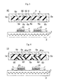
- Figs. 2(a) and 2(b) are processing diagrams illustrating an example of a mounting method using a mounting device of the present embodiment.
- the wiring board 10 is disposed on the base 2, and an anisotropic conductive adhesive film 7 is placed on the wiring board 10.
- the anisotropic conductive adhesive film 7 is formed by dispersing conductive particles 7b in binder resin 7a.
- the melt viscosity of the adhesive film 7 when used as the adhesive agent in the present invention is not affected by the presence/absence of the dispersed conductive particles 7b.
- the IC chip 20 is placed on this anisotropic conductive adhesive film 7 and the pressure bonding surface 6a of the thermocompression bonding head 4 is pressed against the top portion 20a of the IC chip 20 via a protective film (not shown) to perform temporary pressure bonding under predetermined conditions. Further, pressure bonding is performed under the conditions described below.
- the IC chip 20 side is heated at a predetermined temperature and the wiring board 10 side is heated at a temperature higher than the above predetermined temperature, during the pressure bonding.
- the heater of the thermocompression bonding head 4 is controlled such that the temperature of the pressure bonding member 6 is set to approximately 100°C, and the heater 3 of the base 2 is controlled such that the temperature of the binder resin 7a of the anisotropic conductive adhesive film 7 is set to approximately 200°C.
- the anisotropic conductive adhesive film 7 as an adhesive agent is heated so that its melt viscosity is not less than 1.0 ⁇ 10 2 mPa ⁇ s and not more than 1.0 ⁇ 10 5 mPa ⁇ s.
- melt viscosity of the anisotropic conductive adhesive film 7 during thermocompression bonding is less than 1.0 ⁇ 10 2 mPa ⁇ s, there is a drawback that the fluidity of the binder resin 7a during thermocompression bonding is large, generating voids and making the initial resistance and the connection reliability poor. If the melt viscosity of the anisotropic conductive adhesive film 7 is more than 1.0 ⁇ 10 5 m Pa ⁇ s, there is a drawback that the binder resin 7a cannot fully be eliminated at the connecting portion during thermocompression bonding, thereby generating voids and making the initial resistance and the connection reliability poor.
- the pressure applied to each IC chip 20 is approximately 100 N for about 15 seconds.
- the fillet portions 7c at the lateral sides of the IC chip 20 also can be pressed with a pressure that is smaller than the pressure applied to the top portion 20a. Accordingly, a sufficient pressure can be applied to the connecting portion of the IC chip 20 and the wiring board 10, and to the fillet portion 7c around the IC chip 20 such that no voids are generated.
- the pressing force of each pressure bonding member 6 is adjusted by the pressing force adjusting frames 5a, such that the top portion 20a and the lateral sides of each IC chip can be pressed with an optimal pressure (particularly, uniform force to the lateral sides of the IC chip 20), when a plurality of IC chips 20 are pressed by the respective pressure bonding members 6 at a time.
- an optimal pressure particularly, uniform force to the lateral sides of the IC chip 20
- FIGs. 3-6 are schematic construction diagrams illustrating other embodiments of the present invention. Elements described in references to Figs. 1(a)-2(b) are assigned with the same reference numerals, and detailed description thereof is omitted.
- the head main body 5 includes a plurality of pressing force adjusting frames 5a provided in the concave portion 5b of the head main body 5.
- a construction is adopted in which these pressing force adjusting frames 5a are buried inside the pressure bonding member 6 that is integrally formed inside the concave portion 5b.
- pressing force adjusting frames 50 positioned between the pressing force adjusting frames 5a are pressing force adjusting frames 50 having shorter lengths than the length of the pressing force adjusting frames 5a, and the lengths of pressing force adjusting frames 50 are differentiated.
- the pressing force can be adjusted for various regions on the pressure bonding surface 6a of the pressure bonding member 6.
- thermocompression bonding heads 4 based on the number, allocation position, size or the like of the IC chip 20, and thermocompression bonding can be performed for a plurality of IC chips 20 simultaneously while preventing positional displacement of the IC chips 20.
- a cut portion 6b is provided as a pressing force adjusting mechanism at the pressure bonding surface 6a of the pressure bonding member 6 that is attached inside the concave portion 5b of the head main body 5.
- a plurality of the cut portions 6b are provided at predetermined intervals. By changing the number, orientation and depth of the cut portions 6b, the pressing force can be adjusted corresponding to each of various regions on the pressure bonding surface 6a of the pressure bonding member 6.
- the gap formed in the cut portion 6b is narrow. Therefore, even when the IC chip 20 is placed directly below the cut portion 6b, the IC chip 20 is not displaced during thermocompression bonding and smooth pressing can be performed at each of various regions on the pressure bonding surface 6a.
- thermocompression bonding heads 4 it is not necessary to prepare the thermocompression bonding heads 4 based on the number, allocation position, size or the like of the IC chip 20.
- a further advantage is that thermocompression bonding can be performed for a plurality of IC chips 20 simultaneously without positional displacement of the IC chips 20.
- a mounting device 1C in accordance with an embodiment of the invention is shown in Fig. 5 and combines features of the embodiment shown in Fig. 3 and the embodiment shown in Fig. 4.
- the pressing force adjusting frames 5a and 50 are buried inside the pressure bonding member 6 provided in the concave portion 5b of the head main body 5. Cut portions 6b are provided in the pressure bonding surface 6a of the pressure bonding member 6.
- thermocompression bonding head 4 it is not required to prepare the thermocompression bonding head 4 based on the number, allocation position, size or the like of the IC chip 20, and thermocompression bonding can be performed for a plurality of IC chips 20 simultaneously while avoiding positional displacement of the IC chips 20.
- the pressing force adjusting frames 5a and 50 of the head main body 5 and the cut portions 6b of the pressure bonding member 6 are used jointly to form the pressing force adjusting mechanism, it is possible to finely adjust the pressing force applied by various regions on the pressure bonding surface 6a of the pressure bonding member 6.
- a mounting device 1D shown in Fig. 6 is configured such that the pressing force adjusting frames 5a are buried inside the pressure bonding member 6 provided in the concave portion 5b of the head main body 5.
- a plurality of (two types in the present embodiment) pressure bonding members 61 and 62 are made to form an integrated construction.
- a construction is adopted in which a rectangular parallelepiped-shaped concave portion, for example, is formed in the first pressure bonding member 61 of the concave portion 5b of the head main body 5, and the second pressure bonding member 62 having the same shape as the concave portion formed in the first pressure bonding member 61 is fitted into the concave portion, thereby forming the flat pressure bonding surface 6a.
- the second pressure bonding member 62 is penetrated by the pressing force adjusting frames 5a of the head main body 5 to be supported by the same, and fixed with an adhesive agent, for example, to an interface 61a of the first pressure bonding member 61 on the side of the concave portion 5a of the head main body 5.
- a gap 60 is formed between a lateral side surface of the second pressure bonding member 62 and the lateral surface of the first pressure bonding member 61.
- the gap 60 as similar to the cut portion 6b is formed between the first and second pressure bonding members 61 and 62, it is possible to prevent positional displacement of the IC chip 20 by a simple method without the need for a frame portion.
- the gap 60 is narrow such that even when the IC chip 20 is placed directly below the gap 60, the IC chip 20 is not displaced during thermocompression bonding.
- the second pressure bonding member 62 from a material whose rubber hardness degree is lower than that of the first pressure bonding member 61.
- thermocompression bonding head 4 it is not required to prepare the thermocompression bonding head 4 based on the number, allocation position, size or the like of the IC chip 20, and thermocompression bonding can be performed for a plurality of IC chips 20 simultaneously without positional displacement of the IC chips 20.
- frame-shaped pressing force adjusting portions are provided as the pressing force adjusting mechanism in the head main body.
- the present invention is not limited to this and the pressing force adjusting portion can be a protrusion as described below.
- a construction is adopted in which a plurality of pressing force adjusting portions 51 having the form of protrusions extend from the concave portion 5b inside the pressing force adjusting frame 5a of the head main body 5.
- the height of the pressing force adjusting frame 51 is shorter than that of the pressing force adjusting frame 5a surrounding the same. Accordingly, the pressing force adjusting frame 51 are buried inside the pressure bonding member 6.
- thermocompression bonding heads 4 it is not required to prepare the thermocompression bonding heads 4 based on the number, allocation position, size or the like of the IC chip 20, and thermocompression bonding can be performed for a plurality of IC chips 20 simultaneously without positional displacement of the IC chips 20.
Landscapes
- Engineering & Computer Science (AREA)
- Mechanical Engineering (AREA)
- Physics & Mathematics (AREA)
- Fluid Mechanics (AREA)
- Manufacturing & Machinery (AREA)
- Microelectronics & Electronic Packaging (AREA)
- Wire Bonding (AREA)
- Electric Connection Of Electric Components To Printed Circuits (AREA)
Abstract

Description
- The present invention relates to techniques for mounting electrical components, for example, semiconductor chips or the like on a wiring board, and particularly, to techniques for mounting electrical components using an adhesive agent.
- Conventionally, a method using an anisotropic conductive adhesive film in which conductive particles are dispersed in a binder is known for directly mounting a bear chip on a wiring board such as a printed wiring board.
- In the mounting method using the anisotropic conductive adhesive film, after an IC chip is placed on a board to which the anisotropic conductive adhesive film adheres, pressure/heat is applied to the IC chip by a flat ceramic, metal or other pressure bonding head to cure the anisotropic conductive adhesive film. This is know as mounting by thermocompression bonding.
- One problem associated with such a method that involves applying pressure/heat using a metal or other pressure bonding head is that a fillet portion of an adhesive agent around the IC chip does not become heated sufficiently heated during the thermocompression bonding, thereby reducing connection reliability. Another problem associated with such a method that it is difficult to mount a plurality of IC chips.
- Consequently, in order to solve these problems, techniques have been proposed in recent years that perform thermocompression bonding of IC chips using a thermocompression bonding head made of an elastic body such as silicone rubber (for example, see
Patent Documents 1 and 2). - However, these conventional techniques have a problem that sufficient connection the IC chip and the board cannot be achieved because a sufficient pressurizing force is not applied to a portion between bumps and patterns. As a result, the initial conduction resistance and the connection reliability after aging cannot be sufficiently secured.
- Another disadvantage of a method that involves applying pressure/heat using a thermocompression bonding head made of an elastic body is that displacement occurs between the IC chip and the board during pressure bonding.
- The extent of the displacement tends to increase particularly in the case when a plurality of IC chips are mounted at one time.
Patent document 1:JP 2000-79611A
Patent document 2:JP 2002-359264A - The present invention has been achieved to solve such problems of conventional techniques, and it is an object of the present invention to provide a mounting device that can mount a plurality of electrical components with an adhesive agent in a highly reliable manner.
- The present invention for achieving the above-described purpose provides a mounting device for an electric component that includes a thermocompression bonding head that includes a pressure bonding member made of a predetermined elastomer that is provided in a head main body, and a pressing force adjusting mechanism for adjusting a pressing force corresponding to a region on a pressure bonding surface of the pressure bonding member, wherein the pressure bonding member is pressed at a predetermined pressure towards an electric component placed on a wiring board.
- The present invention provides the mounting device described above, wherein a plurality of frame-shaped pressing force adjusting portions are provided in the head main body as the pressing force adjusting mechanism, and the pressure bonding member is disposed inside the pressing force adjusting portions.
- The present invention provides the mounting device described above, wherein a pressing force adjusting portion in the form of a protrusion is provided in the head main body as the pressing force adjusting mechanism.
- The present invention provides the mounting device described above, wherein the heights of the pressing force adjusting portions are differentiated.
- The present invention provides the mounting device described above, wherein the pressing force adjusting mechanism is buried in the pressure bonding member.
- The present invention provides the mounting device described above, wherein the pressing force adjusting mechanism includes a cut portion in the pressure bonding member.
- The present invention provides the mounting device described above, wherein the pressing force adjusting mechanism comprises a plurality of the pressure bonding members integrally connected.
- The present invention provides the mounting device described above that includes a base for supporting the wiring board, and a heater provided in the base.
- In the present invention, when an electrical component is pressed by a pressure bonding member made of a predetermined elastomer during thermocompression bonding, while a region on the pressed side of the electrical component (for example, a top region opposing the pressure bonding member) is pressed at a predetermined pressure toward the wiring board, a region on the lateral sides of the electrical component is pressed at a smaller pressure than the pressure applied to the region on the pressed side.
- As a result, while sufficient pressure can be applied to a connection portion of the electrical component and the wiring board, pressure can be applied to a fillet portion around the electrical component so as to prevent generation of voids. Accordingly, connection of IC chips, etc. can be performed in a highly reliable manner using an anisotropic conductive adhesive film, for example.
- In addition, in the present invention, a pressing force adjusting mechanism for adjusting the pressing force for each of various regions on a pressure bonding surface of the pressure bonding member is provided, and such that when pressing a plurality of electrical components simultaneously with respective pressure bonding portions, it is possible to press regions on the pressed side and the lateral sides of each electrical component respectively with an optimal force. This result in highly reliable mounting and avoids displacement between each electrical component and the board during the pressure bonding.
- Specifically, in the present invention, a plurality of frame-shaped pressing force adjusting portions as the pressing force adjusting mechanism are provided in the head main body. When the pressure bonding member is arranged inside these pressing force adjusting frame portions, it becomes possible to achieve without fail a condition with respect to a corresponding electrical component that regions on the lateral sides of an electrical component are pressed with a smaller pressure than regions on the pressed side of the electrical component. In addition, since fine adjustment of the materials, hardness degree, and other properties of the pressure bonding member in the pressing force adjusting frame portions is possbile, displacement can be reliably prevented when a large number of electrical components are mounted at simultaneously.
- Furthermore in the present invention, if a pressing force adjusting portion in the form of protrusion is provided in the head main body as the pressing force adjusting mechanism, and/or the pressing force adjusting portions are configured such that the heights of the pressing force adjusting portions are differentiated, the pressing force applied to each of various regions on the pressure bonding surface of the pressure bonding member can be optimazed. Consequently it is possible to perform more reliable thermocompression bonding for a plurality of electrical components simultaneously by avoiding positional displacement of the electrical components.
- In the present invention, a construction is adopted in which the pressing force adjusting mechanism is buried in the pressure bonding member and pressure bonding can be performed even when the electrical component is located directly below the pressing force adjusting mechanism. Consequently, smooth pressing can be performed in various regions on the pressure bonding surface. As a result, it is not necessary to prepare the thermocompression bonding head based on the number, allocation position, size or the like of the electrical component, and thermocompression bonding can be performed for a plurality of electrical components of various types simultaneously, without the disadvantage of positional displacement of the various electrical components.
- Further, in the present invention, a cut portion is provided in the pressure bonding member as the pressing force adjusting mechanism such that only the portion of the pressure bonding member contacting the electrical component is compressed without the pressing force being transmitted to adjacent portions beyond the cut portion. Consequently, it becomes possible to prevent positional displacement of the electrical component by a simple method without forming a frame portion.
- Furthermore, in the present invention, when the pressing force adjusting mechanism comprises a plurality of pressure bonding members integrally formed, the gap similar to the cut portion described above can be formed in the pressure bonding member, so as to prevent positional displacement of the electrical component by a simple method without use of a frame portion.
- According to the present invention, a plurality of electrical components can be mounted with an adhesive agent with a high degree of reliability.
-
- Fig. 1(a) is a schematic construction diagram showing major portions of a mounting device of the present embodiment.
- Fig. 1(b) is an explanatory diagram illustrating the positional relationship between a thermocompression bonding head of a mounting device and IC chips.
- Figs. 2(a) and 2(b) are processing diagrams illustrating an example of a mounting method using the mounting device of the present embodiment.
- Fig. 3 is a schematic construction diagram showing another embodiment of the present invention.
- Fig. 4 is a schematic construction diagram showing yet another embodiment of the present invention.
- Fig. 5 is a schematic construction diagram showing still another embodiment of the present invention.
- Fig. 6 is a schematic construction diagram showing still another embodiment of the present invention.
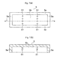
- Fig. 7(a) is a plan view showing a head main body of still another embodiment of the present invention.
- Fig. 7(b) is a cross-sectional view taken along the line A-A in Fig. 7(a).
-
- 1 mounting device
- 2 base
- 3 heater
- 4 thermocompression bonding head
- 5 head main body
- 5a pressing force adjusting frame (frame-shaped pressing force adjusting portion, pressing force adjusting mechanism)
- 6 pressure bonding member
- 6a pressure bonding surface
- 7 anisotropic conductive adhesive film
- 7c fillet portion
- 10 wiring board
- 20 IC chip (electrical component)
- 20a top portion
- In the following, embodiments of a mounting device for electrical components according to the present invention are described in detail through reference to the drawings.
- Fig. 1(a) is a schematic construction diagram showing major portions of a mounting device of the present embodiment, and Fig. 1(b) is an explanatory diagram illustrating the positional relationship between a thermocompression bonding head of the mounting device and IC chips.
- As shown in Figs. 1(a) and 1(b) in accordance with an embodiment of the invention, a mounting
device 1 includes abase 2 that holds awiring board 10 on which awiring pattern 10a is formed, and a thermocompression bonding head 4 for applying pressure and heat to an IC chip (electrical component) 20 having abump 20b. - The
base 2 is made of a predetermined metal and aheater 3 for heating is provided inside thebase 2. - The thermocompression bonding head 4 includes a head
main body 5 made of a predetermined metal, and a heater (not shown) for heating is provided inside thereof. - At a portion of the head
main body 5 opposing thebase 2, a plurality of pressing force adjusting frames (pressing force adjusting mechanism) 5a are provided so as to correspond to a plurality of IC chips 20.Concave portions 5b are provided that are divided into plural spaces by the pressingforce adjusting frames 5a. - In the present embodiment, a
pressure bonding members 6 made of a plate-shaped elastomer is attached to the inner wall of each of theconcave portions 5b. - The
pressure bonding member 6 of the present embodiment is disposed such that a flatpressure bonding surface 6a is in a substantially horizontal position. Thepressure bonding surface 6a of thepressure bonding member 6 is configured to have a larger area than the area of atop portion 20a of theIC chip 20 so as to apply uniform force to thetop portion 20a. - It is preferable that the thickness of the
pressure bonding member 6 is equal to or larger than the thickness of theIC chip 20 in order to apply an optimal pressure to thetop portion 20a and afillet portion 7c (described later) on the lateral sides of theIC chip 20. - The type of elastomer used for the
pressure bonding member 6 of the present invention is not limited. However, it is preferable to use an elastomer whose rubber hardness degree is not less than 40 and not more than 80 to improve connection reliability. - Elastomers having a rubber hardness degree of less than 40 do not apply sufficient pressure to the
IC chip 20. A a result, the initial resistance and connection reliability become poor. If the pressure bonding member is made from an elastomer with a rubber hardness degree of more than 80, insufficient pressure is applied to the fillet portion. This generates voids in a binder resin of an adhesive agent, thereby making the connection reliability poor. - In the present specification, the rubber hardness degree is taken according to JIS S 6050 (room temperature as temperature condition: 5 to 35°C).
- The method used for measuring the rubber hardness degree according to JIS S 6050 is described as follows:
- Using a spring hardness testing machine whose pressing needle has a hemispheric shape with a diameter of 5.08 ± 0.02 mm, a pressing surface of the pressing needle is brought into contact with a surface of a horizontally-retained test piece, with the pressing needle of the testing machine being kept vertical to the surface of the test piece, and a gauge is immediately read in a positive number.
- The entire surface of the test piece is equally divided into three areas, and measurement is performed at a single spot in the central portion for each area. The median value of the measured values is taken as the hardness of the test piece.
- Note 1: The height of the pressing needle is 2.54 ± 0.02 mm when the gauge indicates "0," and 0 mm when the gauge indicates "100."
- Note 2: the relation between the gauge and the spring force (N) is as follows: the spring force (N) is 0.54 when the gauge indicates "0," 1.32 when the gauge indicates "10," 2.11 when the gauge indicates "20," 2.50 when the gauge indicates "25," 2.89 when the gauge indicates "30," 3.68 when the gauge indicates "40," 4.46 when the gauge indicates "50," 5.25 when the gauge indicates "60," 6.03 when the gauge indicates "70," 6.42 when the gauge indicates "75," 6.82 when the gauge indicates "80," 7.60 when the gauge indicates "90," and 8.39 when the gauge indicates "100."
- During experimentation, the inventors confirmed that when the
pressure bonding member 6 was heated from room temperature to 240°C, the rubber hardness degree of the elastomer of thepressure bonding member 6 showed very little change (approximately ± 2). - Both natural rubber and synthetic rubber can be used as the above elastomer. It is preferable to use silicone rubber for its heat resistance and pressure resistance properties.
- Figs. 2(a) and 2(b) are processing diagrams illustrating an example of a mounting method using a mounting device of the present embodiment.
- In order to mount the
IC chip 20 in the present embodiment, refereeing to Fig. 2(a), thewiring board 10 is disposed on thebase 2, and an anisotropic conductiveadhesive film 7 is placed on thewiring board 10. The anisotropic conductiveadhesive film 7 is formed by dispersingconductive particles 7b inbinder resin 7a. - It should be noted that if the amount of the
conductive particles 7b dispersed in thebinder resin 7a is small, the melt viscosity of theadhesive film 7 when used as the adhesive agent in the present invention is not affected by the presence/absence of the dispersedconductive particles 7b. - The
IC chip 20 is placed on this anisotropic conductiveadhesive film 7 and thepressure bonding surface 6a of the thermocompression bonding head 4 is pressed against thetop portion 20a of theIC chip 20 via a protective film (not shown) to perform temporary pressure bonding under predetermined conditions. Further, pressure bonding is performed under the conditions described below. - To reliably prevent the generation of voids by sufficiently heating the
fillet portion 7c around theIC chip 20, it is preferable that theIC chip 20 side is heated at a predetermined temperature and thewiring board 10 side is heated at a temperature higher than the above predetermined temperature, during the pressure bonding. - Specifically, the heater of the thermocompression bonding head 4 is controlled such that the temperature of the
pressure bonding member 6 is set to approximately 100°C, and theheater 3 of thebase 2 is controlled such that the temperature of thebinder resin 7a of the anisotropic conductiveadhesive film 7 is set to approximately 200°C. - In this way, during the thermocompression bonding, the anisotropic conductive
adhesive film 7 as an adhesive agent is heated so that its melt viscosity is not less than 1.0×10²mPa·s and not more than 1.0×10⁵ mPa·s. - If the melt viscosity of the anisotropic conductive
adhesive film 7 during thermocompression bonding is less than 1.0×10² mPa·s, there is a drawback that the fluidity of thebinder resin 7a during thermocompression bonding is large, generating voids and making the initial resistance and the connection reliability poor. If the melt viscosity of the anisotropic conductiveadhesive film 7 is more than 1.0×10⁵m Pa·s, there is a drawback that thebinder resin 7a cannot fully be eliminated at the connecting portion during thermocompression bonding, thereby generating voids and making the initial resistance and the connection reliability poor. - During the thermocompression bonding, the pressure applied to each
IC chip 20 is approximately 100 N for about 15 seconds. - As shown in Fig. 2(b), in the present embodiment, while the
top portion 20a of the1C chip 20 is pressed toward thewiring board 10 with a predetermined pressure by pressurizing thepressure bonding member 6 made of the above-described elastomer, thefillet portions 7c at the lateral sides of theIC chip 20 also can be pressed with a pressure that is smaller than the pressure applied to thetop portion 20a. Accordingly, a sufficient pressure can be applied to the connecting portion of theIC chip 20 and thewiring board 10, and to thefillet portion 7c around theIC chip 20 such that no voids are generated. - As a result, according to the present embodiment, high reliable connection of the
IC chip 20 or the like can be obtained using the anisotropic conductiveadhesive film 7. - Furthermore, in the present embodiment, the pressing force of each
pressure bonding member 6 is adjusted by the pressingforce adjusting frames 5a, such that thetop portion 20a and the lateral sides of each IC chip can be pressed with an optimal pressure (particularly, uniform force to the lateral sides of the IC chip 20), when a plurality ofIC chips 20 are pressed by the respectivepressure bonding members 6 at a time. As a result, in this embodiment, it is possible to prevent displacement between eachIC chip 20 and theboard 10 during pressure bonding, thereby making the mounting highly reliable. - Figs. 3-6 are schematic construction diagrams illustrating other embodiments of the present invention. Elements described in references to Figs. 1(a)-2(b) are assigned with the same reference numerals, and detailed description thereof is omitted.
- In a mounting
apparatus 1A in accordance with an embodiment of the invention shown in Fig. 3, the headmain body 5 includes a plurality of pressingforce adjusting frames 5a provided in theconcave portion 5b of the headmain body 5. In this embodiment, a construction is adopted in which these pressingforce adjusting frames 5a are buried inside thepressure bonding member 6 that is integrally formed inside theconcave portion 5b. - In addition, positioned between the pressing
force adjusting frames 5a are pressingforce adjusting frames 50 having shorter lengths than the length of the pressingforce adjusting frames 5a, and the lengths of pressingforce adjusting frames 50 are differentiated. - In the present embodiment, by changing the position and the length of the pressing
force adjusting frames pressure bonding surface 6a of thepressure bonding member 6. - With the present embodiment configured as described above, because it is possible to perform pressure bonding even when the
IC chip 20 and thewiring board 10 are directly below the pressingforce adjusting frame 5a, smooth pressing can be performed in various regions on thepressure bonding surface 6a. As a result, it is not required to prepare the thermocompression bonding heads 4 based on the number, allocation position, size or the like of theIC chip 20, and thermocompression bonding can be performed for a plurality ofIC chips 20 simultaneously while preventing positional displacement of the IC chips 20. - Other construction and effects are the same as the above-described embodiment, and detailed description thereof is omitted.
- In a mounting
device 1B shown in Fig. 4, acut portion 6b is provided as a pressing force adjusting mechanism at thepressure bonding surface 6a of thepressure bonding member 6 that is attached inside theconcave portion 5b of the headmain body 5. - In this embodiment, a plurality of the
cut portions 6b are provided at predetermined intervals. By changing the number, orientation and depth of thecut portions 6b, the pressing force can be adjusted corresponding to each of various regions on thepressure bonding surface 6a of thepressure bonding member 6. - With the present embodiment configured as described above, for example, when the
IC chip 20 is pressed by a portion of thepressure bonding surface 6a other than thecut portion 6b, only the direct pressing portion of thepressure bonding surface 6a can be compressed without the pressing force being transmitted to adjacent portions ofpressure bonding surface 6a beyond thecut portion 6b. Consequently, it is possible to prevent positional displacement of theIC chip 20 by a simple method without the need to form the frame portion. - It should be noted that the gap formed in the
cut portion 6b is narrow. Therefore, even when theIC chip 20 is placed directly below thecut portion 6b, theIC chip 20 is not displaced during thermocompression bonding and smooth pressing can be performed at each of various regions on thepressure bonding surface 6a. - Advantage of the present embodiment configured as described above, it is not necessary to prepare the thermocompression bonding heads 4 based on the number, allocation position, size or the like of the
IC chip 20. A further advantage is that thermocompression bonding can be performed for a plurality ofIC chips 20 simultaneously without positional displacement of the IC chips 20. - Other construction and effects are the same as the above-described embodiment, and detailed description thereof is omitted.
- A mounting
device 1C in accordance with an embodiment of the invention is shown in Fig. 5 and combines features of the embodiment shown in Fig. 3 and the embodiment shown in Fig. 4. - In the present embodiment, the pressing
force adjusting frames pressure bonding member 6 provided in theconcave portion 5b of the headmain body 5. Cutportions 6b are provided in thepressure bonding surface 6a of thepressure bonding member 6. - With the present embodiment configured as described above, it is not required to prepare the thermocompression bonding head 4 based on the number, allocation position, size or the like of the
IC chip 20, and thermocompression bonding can be performed for a plurality ofIC chips 20 simultaneously while avoiding positional displacement of the IC chips 20. - Especially in the present embodiment, since a construction is adopted in which the pressing
force adjusting frames main body 5 and thecut portions 6b of thepressure bonding member 6 are used jointly to form the pressing force adjusting mechanism, it is possible to finely adjust the pressing force applied by various regions on thepressure bonding surface 6a of thepressure bonding member 6. - Other structure and effects are the same as the above-described embodiment, and detailed description thereof is omitted.
- A mounting
device 1D shown in Fig. 6 is configured such that the pressingforce adjusting frames 5a are buried inside thepressure bonding member 6 provided in theconcave portion 5b of the headmain body 5. A plurality of (two types in the present embodiment)pressure bonding members - As shown in Fig. 6, in the present embodiment, a construction is adopted in which a rectangular parallelepiped-shaped concave portion, for example, is formed in the first
pressure bonding member 61 of theconcave portion 5b of the headmain body 5, and the secondpressure bonding member 62 having the same shape as the concave portion formed in the firstpressure bonding member 61 is fitted into the concave portion, thereby forming the flatpressure bonding surface 6a. - In this embodiment, the second
pressure bonding member 62 is penetrated by the pressingforce adjusting frames 5a of the headmain body 5 to be supported by the same, and fixed with an adhesive agent, for example, to aninterface 61a of the firstpressure bonding member 61 on the side of theconcave portion 5a of the headmain body 5. - A
gap 60 is formed between a lateral side surface of the secondpressure bonding member 62 and the lateral surface of the firstpressure bonding member 61. - According to the present embodiment configured as described above, since the
gap 60 as similar to thecut portion 6b is formed between the first and secondpressure bonding members IC chip 20 by a simple method without the need for a frame portion. - In this embodiment, same as in the above embodiment, the
gap 60 is narrow such that even when theIC chip 20 is placed directly below thegap 60, theIC chip 20 is not displaced during thermocompression bonding. - From the viewpoint of reliably achieving the effect of the present invention and improving connection reliability, it is preferable to make the second
pressure bonding member 62 from a material whose rubber hardness degree is lower than that of the firstpressure bonding member 61. - According to the present embodiment configured as described above, it is not required to prepare the thermocompression bonding head 4 based on the number, allocation position, size or the like of the
IC chip 20, and thermocompression bonding can be performed for a plurality ofIC chips 20 simultaneously without positional displacement of the IC chips 20. - Other construction and effects are the same as the above-described embodiment so that detailed description thereof is omitted.
- The invention is not limited to the above-described embodiments, and various modifications are possible.
- For example, in the above-described embodiments, frame-shaped pressing force adjusting portions are provided as the pressing force adjusting mechanism in the head main body. However, the present invention is not limited to this and the pressing force adjusting portion can be a protrusion as described below.
- For example, in the embodiment illustrated in Figs. 7(a) and 7(b), a construction is adopted in which a plurality of pressing
force adjusting portions 51 having the form of protrusions extend from theconcave portion 5b inside the pressingforce adjusting frame 5a of the headmain body 5. - The height of the pressing
force adjusting frame 51 is shorter than that of the pressingforce adjusting frame 5a surrounding the same. Accordingly, the pressingforce adjusting frame 51 are buried inside thepressure bonding member 6. - In accordance with the present embodiment configured as described above, it is not required to prepare the thermocompression bonding heads 4 based on the number, allocation position, size or the like of the
IC chip 20, and thermocompression bonding can be performed for a plurality ofIC chips 20 simultaneously without positional displacement of the IC chips 20. - In the above-described embodiment, a case in which an IC chip is mounted using an anisotropic conductive adhesive film is described as an example. However, the present invention is not limited to this. An adhesive agent that does not contain conductive particles may also be used.
- In the above-described embodiment, a case is described as an example in which an IC chip having a bump electrode is mounted. However, an IC chip that does not include a bump electrode can also be used.
Claims (8)
- A mounting device for an electric component, comprising:a thermocompression bonding head comprising a pressure bonding member made of a predetermined elastomer, the pressure bonding member provided in a head main body, anda pressing force adjusting mechanism for adjusting a pressing force corresponding to a region on a pressure bonding surface of the pressure bonding member,wherein the pressure bonding member is pressed at a predetermined pressure toward an electric component placed on a wiring board.
- The mounting device according to claim 1, wherein a the pressing force adjusting mechanism comprises a plurality of frame-shaped pressing force adjusting portions provided in the head main body and the pressure bonding member is disposed inside the pressing force adjusting portions.
- The mounting device according to claim 1, wherein the pressing force adjusting mechanism comprises a pressing force adjusting portion in the form of a protrusion provided inside the head main body.
- The mounting device according to claim 2 or 3, wherein heights of the pressing force adjusting portions are differentiated.
- The mounting device according to claim 1, wherein the pressing force adjusting mechanism is buried in the pressure bonding member.
- The mounting device according to claim 1, wherein the pressing force adjusting mechanism comprises a cut portion in the pressure bonding member.
- The mounting device according to claim 1, wherein the pressing force adjusting mechanism comprises a plurality of pressure bonding members integrally formed.
- The mounting device according to claim 1, further comprising a base for supporting the wiring board, and a heater provided in the base.
Priority Applications (1)
| Application Number | Priority Date | Filing Date | Title |
|---|---|---|---|
| EP10183623A EP2264748A3 (en) | 2005-02-02 | 2006-01-26 | Electric component mounting apparatus |
Applications Claiming Priority (2)
| Application Number | Priority Date | Filing Date | Title |
|---|---|---|---|
| JP2005026787 | 2005-02-02 | ||
| PCT/JP2006/301202 WO2006082744A1 (en) | 2005-02-02 | 2006-01-26 | Electric component mounting apparatus |
Publications (2)
| Publication Number | Publication Date |
|---|---|
| EP1845556A1 true EP1845556A1 (en) | 2007-10-17 |
| EP1845556A4 EP1845556A4 (en) | 2010-02-10 |
Family
ID=36777132
Family Applications (2)
| Application Number | Title | Priority Date | Filing Date |
|---|---|---|---|
| EP10183623A Withdrawn EP2264748A3 (en) | 2005-02-02 | 2006-01-26 | Electric component mounting apparatus |
| EP06712384A Withdrawn EP1845556A4 (en) | 2005-02-02 | 2006-01-26 | APPARATUS FOR MOUNTING ELECTRICAL COMPONENTS |
Family Applications Before (1)
| Application Number | Title | Priority Date | Filing Date |
|---|---|---|---|
| EP10183623A Withdrawn EP2264748A3 (en) | 2005-02-02 | 2006-01-26 | Electric component mounting apparatus |
Country Status (7)
| Country | Link |
|---|---|
| US (1) | US7857028B2 (en) |
| EP (2) | EP2264748A3 (en) |
| JP (1) | JP4841431B2 (en) |
| KR (1) | KR101253794B1 (en) |
| CN (1) | CN100557783C (en) |
| TW (1) | TWI335631B (en) |
| WO (1) | WO2006082744A1 (en) |
Cited By (2)
| Publication number | Priority date | Publication date | Assignee | Title |
|---|---|---|---|---|
| EP1975994A4 (en) * | 2006-01-13 | 2010-02-17 | Sony Chem & Inf Device Corp | PRESSURE COLLAGE DEVICE AND CORRESPONDING MOUNTING METHOD |
| EP2779219A4 (en) * | 2011-11-07 | 2015-11-04 | Dexerials Corp | BONDING DEVICE, METHOD FOR MANUFACTURING BONDING STRUCTURE, METHOD FOR MANUFACTURING STACKED BUNK COMPONENT, AND METHOD FOR MOUNTING ELECTRONIC COMPONENT |
Families Citing this family (36)
| Publication number | Priority date | Publication date | Assignee | Title |
|---|---|---|---|---|
| JP4206320B2 (en) | 2003-09-19 | 2009-01-07 | 株式会社ルネサステクノロジ | Manufacturing method of semiconductor integrated circuit device |
| KR101253794B1 (en) | 2005-02-02 | 2013-04-12 | 데쿠세리아루즈 가부시키가이샤 | Electric component mounting apparatus |
| JP4979288B2 (en) * | 2006-07-19 | 2012-07-18 | ソニーケミカル&インフォメーションデバイス株式会社 | Mounting method using thermocompression bonding head |
| JP5122192B2 (en) * | 2007-07-04 | 2013-01-16 | パナソニック株式会社 | Semiconductor device mounting equipment |
| JP2009141269A (en) * | 2007-12-10 | 2009-06-25 | Sony Chemical & Information Device Corp | Mounting method and mounting apparatus for electrical parts |
| JP4916494B2 (en) * | 2008-08-08 | 2012-04-11 | ソニーケミカル&インフォメーションデバイス株式会社 | Crimping apparatus, crimping method, and pressing plate |
| JP2011109046A (en) * | 2009-11-20 | 2011-06-02 | Sony Chemical & Information Device Corp | Mounting apparatus and method for manufacturing electronic module |
| JP5602439B2 (en) * | 2010-01-22 | 2014-10-08 | デクセリアルズ株式会社 | Heating device and manufacturing method of mounting body |
| WO2011132384A1 (en) * | 2010-04-23 | 2011-10-27 | 住友ベークライト株式会社 | Device and method for producing electronic device, and pair of compressed members thereof |
| KR20120009713A (en) * | 2010-07-20 | 2012-02-02 | 삼성전자주식회사 | Apparatus for manufacturing printed circuit board assembly and method for manufacturing same |
| US8381965B2 (en) | 2010-07-22 | 2013-02-26 | Taiwan Semiconductor Manufacturing Company, Ltd. | Thermal compress bonding |
| US8651359B2 (en) * | 2010-08-23 | 2014-02-18 | International Business Machines Corporation | Flip chip bonder head for forming a uniform fillet |
| US8104666B1 (en) | 2010-09-01 | 2012-01-31 | Taiwan Semiconductor Manufacturing Company, Ltd. | Thermal compressive bonding with separate die-attach and reflow processes |
| US8177862B2 (en) | 2010-10-08 | 2012-05-15 | Taiwan Semiconductor Manufacturing Co., Ltd | Thermal compressive bond head |
| JP5437221B2 (en) * | 2010-11-29 | 2014-03-12 | アルファーデザイン株式会社 | Bonding equipment |
| JP5732239B2 (en) * | 2010-11-30 | 2015-06-10 | デクセリアルズ株式会社 | Thermocompression head, thermocompression bonding equipment, mounting method |
| CN102426919A (en) * | 2011-08-17 | 2012-04-25 | 六和电子(江西)有限公司 | Production process for low-noise metallic film capacitor |
| US9842817B2 (en) * | 2012-02-27 | 2017-12-12 | Taiwan Semiconductor Manufacturing Company, Ltd. | Solder bump stretching method and device for performing the same |
| US8912045B2 (en) * | 2012-06-12 | 2014-12-16 | International Business Machines Corporation | Three dimensional flip chip system and method |
| KR102170192B1 (en) * | 2013-08-22 | 2020-10-26 | 삼성전자주식회사 | Bonding apparatus , bonding method, and method for manufacturing substrates |
| DE102014114096A1 (en) | 2014-09-29 | 2016-03-31 | Danfoss Silicon Power Gmbh | Sintering tool for the lower punch of a sintering device |
| DE102014114095B4 (en) | 2014-09-29 | 2017-03-23 | Danfoss Silicon Power Gmbh | sintering apparatus |
| DE102014114093B4 (en) | 2014-09-29 | 2017-03-23 | Danfoss Silicon Power Gmbh | Method for low-temperature pressure sintering |
| DE102014114097B4 (en) | 2014-09-29 | 2017-06-01 | Danfoss Silicon Power Gmbh | Sintering tool and method for sintering an electronic assembly |
| DE102017106536A1 (en) * | 2016-03-29 | 2017-10-05 | Panasonic Intellectual Property Management Co., Ltd. | Method for producing a solar cell module |
| KR101996936B1 (en) * | 2018-12-19 | 2019-07-05 | (주)제이스텍 | Back-Up Heating Bonding Unit |
| CN111526673A (en) * | 2019-02-01 | 2020-08-11 | 泰拉丁公司 | maintain the shape of the board |
| JP7301468B2 (en) * | 2019-04-17 | 2023-07-03 | 株式会社ディスコ | Workpiece processing method, thermocompression bonding method |
| US11676937B2 (en) * | 2021-05-04 | 2023-06-13 | Asmpt Singapore Pte. Ltd. | Flexible sinter tool for bonding semiconductor devices |
| KR102573094B1 (en) * | 2021-05-11 | 2023-09-01 | 정라파엘 | Method of bonding a die |
| US12604754B2 (en) | 2022-03-31 | 2026-04-14 | Intel Corporation | Package structures with non-uniform interconnect features |
| US12598989B2 (en) | 2022-03-31 | 2026-04-07 | Intel Corporation | Package structures with patterned die backside layer |
| US12604733B2 (en) | 2022-03-31 | 2026-04-14 | Intel Corporation | Package structures with collapse control features |
| US20230317676A1 (en) * | 2022-04-01 | 2023-10-05 | Intel Corporation | Bond head design for thermal compression bonding |
| US12599022B2 (en) * | 2022-07-22 | 2026-04-07 | Asmpt Singapore Pte. Ltd. | Apparatus for applying a sintering force via a compressible film |
| CN115938964A (en) * | 2022-11-24 | 2023-04-07 | 长鑫存储技术有限公司 | Pressurized parts, thermocompression horns and thermocompression devices |
Family Cites Families (17)
| Publication number | Priority date | Publication date | Assignee | Title |
|---|---|---|---|---|
| US4875966A (en) * | 1988-09-12 | 1989-10-24 | General Dynamics Corp., Pomona Div. | Pressure transfer plate assembly for a heat bonding apparatus |
| US5186632A (en) * | 1991-09-20 | 1993-02-16 | International Business Machines Corporation | Electronic device elastomeric mounting and interconnection technology |
| DE4233073A1 (en) * | 1992-10-01 | 1994-04-07 | Siemens Ag | Semiconductor modular structure prodn. - by convexly shaping and bonding in single hot pressing operation |
| JP4077982B2 (en) | 1998-06-26 | 2008-04-23 | 日機装株式会社 | Mold for pressure molding |
| JP3663931B2 (en) * | 1998-08-25 | 2005-06-22 | セイコーエプソン株式会社 | Crimping method, crimping apparatus, and liquid crystal display device manufacturing method |
| US6414397B1 (en) * | 1998-12-02 | 2002-07-02 | Seiko Epson Corporation | Anisotropic conductive film, method of mounting semiconductor chip, and semiconductor device |
| JP3815149B2 (en) * | 1999-11-04 | 2006-08-30 | セイコーエプソン株式会社 | Component mounting method and electro-optical device manufacturing method |
| US6484776B1 (en) * | 2000-04-07 | 2002-11-26 | Northrop Grumman Corporation | System for constructing a laminate |
| JP2002324821A (en) * | 2001-04-25 | 2002-11-08 | Matsushita Electric Ind Co Ltd | Electronic component crimping apparatus and crimping method |
| JP4513235B2 (en) | 2001-05-31 | 2010-07-28 | ソニー株式会社 | Flip chip mounting device |
| JP4710205B2 (en) * | 2001-09-06 | 2011-06-29 | ソニー株式会社 | Flip chip mounting method |
| JP4718734B2 (en) * | 2001-09-12 | 2011-07-06 | 日機装株式会社 | Circuit element mounting method |
| JP2003258413A (en) * | 2002-03-06 | 2003-09-12 | Nikkiso Co Ltd | Circuit device mounting apparatus and mounting method |
| JP2003298226A (en) * | 2002-03-29 | 2003-10-17 | Optrex Corp | Board connection device |
| JP3798995B2 (en) * | 2002-06-07 | 2006-07-19 | Towa株式会社 | Underfill resin molding method and mold |
| JP3921459B2 (en) * | 2003-07-11 | 2007-05-30 | ソニーケミカル&インフォメーションデバイス株式会社 | Mounting method and mounting apparatus for electrical parts |
| KR101253794B1 (en) | 2005-02-02 | 2013-04-12 | 데쿠세리아루즈 가부시키가이샤 | Electric component mounting apparatus |
-
2006
- 2006-01-26 KR KR1020077019961A patent/KR101253794B1/en not_active Expired - Fee Related
- 2006-01-26 EP EP10183623A patent/EP2264748A3/en not_active Withdrawn
- 2006-01-26 EP EP06712384A patent/EP1845556A4/en not_active Withdrawn
- 2006-01-26 CN CNB2006800037724A patent/CN100557783C/en not_active Expired - Fee Related
- 2006-01-26 JP JP2006523461A patent/JP4841431B2/en not_active Expired - Fee Related
- 2006-01-26 WO PCT/JP2006/301202 patent/WO2006082744A1/en not_active Ceased
- 2006-01-27 TW TW095103361A patent/TWI335631B/en not_active IP Right Cessation
-
2007
- 2007-07-30 US US11/882,049 patent/US7857028B2/en not_active Expired - Fee Related
Cited By (3)
| Publication number | Priority date | Publication date | Assignee | Title |
|---|---|---|---|---|
| EP1975994A4 (en) * | 2006-01-13 | 2010-02-17 | Sony Chem & Inf Device Corp | PRESSURE COLLAGE DEVICE AND CORRESPONDING MOUNTING METHOD |
| EP2779219A4 (en) * | 2011-11-07 | 2015-11-04 | Dexerials Corp | BONDING DEVICE, METHOD FOR MANUFACTURING BONDING STRUCTURE, METHOD FOR MANUFACTURING STACKED BUNK COMPONENT, AND METHOD FOR MOUNTING ELECTRONIC COMPONENT |
| US9196599B2 (en) | 2011-11-07 | 2015-11-24 | Dexerials Corporation | Connection device, method for manufacturing connection structure, method for manufacturing stacked chip component and method for mounting electronic component |
Also Published As
| Publication number | Publication date |
|---|---|
| WO2006082744A1 (en) | 2006-08-10 |
| TWI335631B (en) | 2011-01-01 |
| TW200636894A (en) | 2006-10-16 |
| US7857028B2 (en) | 2010-12-28 |
| HK1116920A1 (en) | 2009-01-02 |
| CN100557783C (en) | 2009-11-04 |
| EP1845556A4 (en) | 2010-02-10 |
| JP4841431B2 (en) | 2011-12-21 |
| EP2264748A2 (en) | 2010-12-22 |
| KR101253794B1 (en) | 2013-04-12 |
| US20080035274A1 (en) | 2008-02-14 |
| JPWO2006082744A1 (en) | 2008-06-26 |
| EP2264748A3 (en) | 2012-09-05 |
| CN101111932A (en) | 2008-01-23 |
| KR20070099679A (en) | 2007-10-09 |
Similar Documents
| Publication | Publication Date | Title |
|---|---|---|
| US7857028B2 (en) | Mounting device for electrical component | |
| US7556190B2 (en) | Method and device for mounting electric component | |
| EP1445995B1 (en) | Method of mounting an electronic component on a circuit board and system for carrying out the method | |
| KR101398307B1 (en) | Method and apparatus for mounting electric parts | |
| US8163599B2 (en) | Flip-chip mounting method, flip-chip mounting apparatus and tool protection sheet used in flip-chip mounting apparatus | |
| KR101034166B1 (en) | Mounting method using thermocompression head | |
| JP2011009357A (en) | Mounting device | |
| JP2010067922A (en) | Thermocompression bonding device and packaging method of electrical component | |
| KR101141990B1 (en) | Method and apparatus for mounting electric component | |
| KR20110039510A (en) | Crimping device, crimping method, mounting body and pressing plate | |
| KR20090029700A (en) | Thermocompression Heads and Mounting Devices Using Them | |
| JP5361134B2 (en) | Pressure head and component crimping device | |
| US7958632B2 (en) | Flexible printed-circuit boards bonding method and printed circuit board | |
| HK1116920B (en) | Electric component mounting apparatus | |
| TWI420995B (en) | Method of assembling electrical components | |
| JP2009032845A (en) | Thermocompression bonding apparatus and electrical component mounting method | |
| JPH09178808A (en) | Inspection equipment for semiconductor devices | |
| JP2006294730A (en) | Semiconductor device manufacturing method and semiconductor device manufacturing apparatus | |
| HK1144853B (en) | Method and apparatus for mounting electric component |
Legal Events
| Date | Code | Title | Description |
|---|---|---|---|
| PUAI | Public reference made under article 153(3) epc to a published international application that has entered the european phase |
Free format text: ORIGINAL CODE: 0009012 |
|
| 17P | Request for examination filed |
Effective date: 20070731 |
|
| AK | Designated contracting states |
Kind code of ref document: A1 Designated state(s): DE NL |
|
| RIN1 | Information on inventor provided before grant (corrected) |
Inventor name: KANISAWA, SHIYUKI |
|
| DAX | Request for extension of the european patent (deleted) | ||
| RBV | Designated contracting states (corrected) |
Designated state(s): DE NL |
|
| A4 | Supplementary search report drawn up and despatched |
Effective date: 20100111 |
|
| RIC1 | Information provided on ipc code assigned before grant |
Ipc: H01L 21/60 20060101AFI20060815BHEP Ipc: H05K 3/30 20060101ALI20100104BHEP |
|
| 17Q | First examination report despatched |
Effective date: 20100330 |
|
| RAP1 | Party data changed (applicant data changed or rights of an application transferred) |
Owner name: DEXERIALS CORPORATION |
|
| STAA | Information on the status of an ep patent application or granted ep patent |
Free format text: STATUS: THE APPLICATION IS DEEMED TO BE WITHDRAWN |
|
| 18D | Application deemed to be withdrawn |
Effective date: 20140801 |