EP1840971A1 - Organic electroluminescent device and fabrication methods thereof - Google Patents
Organic electroluminescent device and fabrication methods thereof Download PDFInfo
- Publication number
- EP1840971A1 EP1840971A1 EP06112123A EP06112123A EP1840971A1 EP 1840971 A1 EP1840971 A1 EP 1840971A1 EP 06112123 A EP06112123 A EP 06112123A EP 06112123 A EP06112123 A EP 06112123A EP 1840971 A1 EP1840971 A1 EP 1840971A1
- Authority
- EP
- European Patent Office
- Prior art keywords
- photo sensor
- layer
- overlying
- gate
- organic electroluminescent
- Prior art date
- Legal status (The legal status is an assumption and is not a legal conclusion. Google has not performed a legal analysis and makes no representation as to the accuracy of the status listed.)
- Withdrawn
Links
- 238000000034 method Methods 0.000 title claims description 6
- 238000004519 manufacturing process Methods 0.000 title description 2
- 239000003990 capacitor Substances 0.000 claims abstract description 19
- 239000000758 substrate Substances 0.000 claims abstract description 17
- 238000005286 illumination Methods 0.000 claims abstract description 9
- 239000010409 thin film Substances 0.000 claims abstract description 6
- 238000002161 passivation Methods 0.000 claims description 10
- 229910021420 polycrystalline silicon Inorganic materials 0.000 claims description 8
- 229920005591 polysilicon Polymers 0.000 claims description 8
- AMGQUBHHOARCQH-UHFFFAOYSA-N indium;oxotin Chemical compound [In].[Sn]=O AMGQUBHHOARCQH-UHFFFAOYSA-N 0.000 claims description 4
- 238000000059 patterning Methods 0.000 claims description 3
- YVTHLONGBIQYBO-UHFFFAOYSA-N zinc indium(3+) oxygen(2-) Chemical compound [O--].[Zn++].[In+3] YVTHLONGBIQYBO-UHFFFAOYSA-N 0.000 claims description 2
- 229910052581 Si3N4 Inorganic materials 0.000 description 9
- HQVNEWCFYHHQES-UHFFFAOYSA-N silicon nitride Chemical compound N12[Si]34N5[Si]62N3[Si]51N64 HQVNEWCFYHHQES-UHFFFAOYSA-N 0.000 description 9
- VYPSYNLAJGMNEJ-UHFFFAOYSA-N Silicium dioxide Chemical compound O=[Si]=O VYPSYNLAJGMNEJ-UHFFFAOYSA-N 0.000 description 8
- 239000000463 material Substances 0.000 description 6
- 229910052814 silicon oxide Inorganic materials 0.000 description 6
- 238000005530 etching Methods 0.000 description 5
- 229920002120 photoresistant polymer Polymers 0.000 description 4
- XUIMIQQOPSSXEZ-UHFFFAOYSA-N Silicon Chemical compound [Si] XUIMIQQOPSSXEZ-UHFFFAOYSA-N 0.000 description 3
- 238000001459 lithography Methods 0.000 description 3
- 239000002184 metal Substances 0.000 description 3
- 229910052751 metal Inorganic materials 0.000 description 3
- 229910052710 silicon Inorganic materials 0.000 description 3
- 239000010703 silicon Substances 0.000 description 3
- 230000008878 coupling Effects 0.000 description 2
- 238000010168 coupling process Methods 0.000 description 2
- 238000005859 coupling reaction Methods 0.000 description 2
- 238000000151 deposition Methods 0.000 description 2
- 230000008021 deposition Effects 0.000 description 2
- 239000002019 doping agent Substances 0.000 description 2
- 230000014509 gene expression Effects 0.000 description 2
- 230000005525 hole transport Effects 0.000 description 2
- 238000002347 injection Methods 0.000 description 2
- 239000007924 injection Substances 0.000 description 2
- 150000002500 ions Chemical class 0.000 description 2
- 230000004048 modification Effects 0.000 description 2
- 238000012986 modification Methods 0.000 description 2
- 230000008569 process Effects 0.000 description 2
- 239000004642 Polyimide Substances 0.000 description 1
- 230000032683 aging Effects 0.000 description 1
- 229910052782 aluminium Inorganic materials 0.000 description 1
- 229910021417 amorphous silicon Inorganic materials 0.000 description 1
- 230000015572 biosynthetic process Effects 0.000 description 1
- 238000005229 chemical vapour deposition Methods 0.000 description 1
- 239000003086 colorant Substances 0.000 description 1
- 238000010586 diagram Methods 0.000 description 1
- 239000003989 dielectric material Substances 0.000 description 1
- 239000010408 film Substances 0.000 description 1
- 239000011521 glass Substances 0.000 description 1
- 230000005283 ground state Effects 0.000 description 1
- BHEPBYXIRTUNPN-UHFFFAOYSA-N hydridophosphorus(.) (triplet) Chemical compound [PH] BHEPBYXIRTUNPN-UHFFFAOYSA-N 0.000 description 1
- PJXISJQVUVHSOJ-UHFFFAOYSA-N indium(III) oxide Inorganic materials [O-2].[O-2].[O-2].[In+3].[In+3] PJXISJQVUVHSOJ-UHFFFAOYSA-N 0.000 description 1
- 238000005468 ion implantation Methods 0.000 description 1
- 238000005224 laser annealing Methods 0.000 description 1
- 239000011159 matrix material Substances 0.000 description 1
- 239000000203 mixture Substances 0.000 description 1
- 238000000206 photolithography Methods 0.000 description 1
- 229920001721 polyimide Polymers 0.000 description 1
- 239000002861 polymer material Substances 0.000 description 1
- 238000002310 reflectometry Methods 0.000 description 1
- 230000004044 response Effects 0.000 description 1
- 239000005368 silicate glass Substances 0.000 description 1
- 235000012239 silicon dioxide Nutrition 0.000 description 1
- 239000000377 silicon dioxide Substances 0.000 description 1
- 229910052709 silver Inorganic materials 0.000 description 1
Images


Classifications
-
- H—ELECTRICITY
- H10—SEMICONDUCTOR DEVICES; ELECTRIC SOLID-STATE DEVICES NOT OTHERWISE PROVIDED FOR
- H10K—ORGANIC ELECTRIC SOLID-STATE DEVICES
- H10K59/00—Integrated devices, or assemblies of multiple devices, comprising at least one organic light-emitting element covered by group H10K50/00
- H10K59/10—OLED displays
- H10K59/12—Active-matrix OLED [AMOLED] displays
- H10K59/13—Active-matrix OLED [AMOLED] displays comprising photosensors that control luminance
-
- H—ELECTRICITY
- H10—SEMICONDUCTOR DEVICES; ELECTRIC SOLID-STATE DEVICES NOT OTHERWISE PROVIDED FOR
- H10K—ORGANIC ELECTRIC SOLID-STATE DEVICES
- H10K71/00—Manufacture or treatment specially adapted for the organic devices covered by this subclass
-
- G—PHYSICS
- G09—EDUCATION; CRYPTOGRAPHY; DISPLAY; ADVERTISING; SEALS
- G09G—ARRANGEMENTS OR CIRCUITS FOR CONTROL OF INDICATING DEVICES USING STATIC MEANS TO PRESENT VARIABLE INFORMATION
- G09G2300/00—Aspects of the constitution of display devices
- G09G2300/08—Active matrix structure, i.e. with use of active elements, inclusive of non-linear two terminal elements, in the pixels together with light emitting or modulating elements
- G09G2300/0809—Several active elements per pixel in active matrix panels
- G09G2300/0842—Several active elements per pixel in active matrix panels forming a memory circuit, e.g. a dynamic memory with one capacitor
-
- G—PHYSICS
- G09—EDUCATION; CRYPTOGRAPHY; DISPLAY; ADVERTISING; SEALS
- G09G—ARRANGEMENTS OR CIRCUITS FOR CONTROL OF INDICATING DEVICES USING STATIC MEANS TO PRESENT VARIABLE INFORMATION
- G09G2320/00—Control of display operating conditions
- G09G2320/04—Maintaining the quality of display appearance
- G09G2320/043—Preventing or counteracting the effects of ageing
- G09G2320/045—Compensation of drifts in the characteristics of light emitting or modulating elements
-
- G—PHYSICS
- G09—EDUCATION; CRYPTOGRAPHY; DISPLAY; ADVERTISING; SEALS
- G09G—ARRANGEMENTS OR CIRCUITS FOR CONTROL OF INDICATING DEVICES USING STATIC MEANS TO PRESENT VARIABLE INFORMATION
- G09G2360/00—Aspects of the architecture of display systems
- G09G2360/14—Detecting light within display terminals, e.g. using a single or a plurality of photosensors
- G09G2360/145—Detecting light within display terminals, e.g. using a single or a plurality of photosensors the light originating from the display screen
- G09G2360/147—Detecting light within display terminals, e.g. using a single or a plurality of photosensors the light originating from the display screen the originated light output being determined for each pixel
- G09G2360/148—Detecting light within display terminals, e.g. using a single or a plurality of photosensors the light originating from the display screen the originated light output being determined for each pixel the light being detected by light detection means within each pixel
-
- G—PHYSICS
- G09—EDUCATION; CRYPTOGRAPHY; DISPLAY; ADVERTISING; SEALS
- G09G—ARRANGEMENTS OR CIRCUITS FOR CONTROL OF INDICATING DEVICES USING STATIC MEANS TO PRESENT VARIABLE INFORMATION
- G09G3/00—Control arrangements or circuits, of interest only in connection with visual indicators other than cathode-ray tubes
- G09G3/20—Control arrangements or circuits, of interest only in connection with visual indicators other than cathode-ray tubes for presentation of an assembly of a number of characters, e.g. a page, by composing the assembly by combination of individual elements arranged in a matrix no fixed position being assigned to or needed to be assigned to the individual characters or partial characters
- G09G3/22—Control arrangements or circuits, of interest only in connection with visual indicators other than cathode-ray tubes for presentation of an assembly of a number of characters, e.g. a page, by composing the assembly by combination of individual elements arranged in a matrix no fixed position being assigned to or needed to be assigned to the individual characters or partial characters using controlled light sources
- G09G3/30—Control arrangements or circuits, of interest only in connection with visual indicators other than cathode-ray tubes for presentation of an assembly of a number of characters, e.g. a page, by composing the assembly by combination of individual elements arranged in a matrix no fixed position being assigned to or needed to be assigned to the individual characters or partial characters using controlled light sources using electroluminescent panels
- G09G3/32—Control arrangements or circuits, of interest only in connection with visual indicators other than cathode-ray tubes for presentation of an assembly of a number of characters, e.g. a page, by composing the assembly by combination of individual elements arranged in a matrix no fixed position being assigned to or needed to be assigned to the individual characters or partial characters using controlled light sources using electroluminescent panels semiconductive, e.g. using light-emitting diodes [LED]
- G09G3/3208—Control arrangements or circuits, of interest only in connection with visual indicators other than cathode-ray tubes for presentation of an assembly of a number of characters, e.g. a page, by composing the assembly by combination of individual elements arranged in a matrix no fixed position being assigned to or needed to be assigned to the individual characters or partial characters using controlled light sources using electroluminescent panels semiconductive, e.g. using light-emitting diodes [LED] organic, e.g. using organic light-emitting diodes [OLED]
- G09G3/3225—Control arrangements or circuits, of interest only in connection with visual indicators other than cathode-ray tubes for presentation of an assembly of a number of characters, e.g. a page, by composing the assembly by combination of individual elements arranged in a matrix no fixed position being assigned to or needed to be assigned to the individual characters or partial characters using controlled light sources using electroluminescent panels semiconductive, e.g. using light-emitting diodes [LED] organic, e.g. using organic light-emitting diodes [OLED] using an active matrix
- G09G3/3233—Control arrangements or circuits, of interest only in connection with visual indicators other than cathode-ray tubes for presentation of an assembly of a number of characters, e.g. a page, by composing the assembly by combination of individual elements arranged in a matrix no fixed position being assigned to or needed to be assigned to the individual characters or partial characters using controlled light sources using electroluminescent panels semiconductive, e.g. using light-emitting diodes [LED] organic, e.g. using organic light-emitting diodes [OLED] using an active matrix with pixel circuitry controlling the current through the light-emitting element
-
- H—ELECTRICITY
- H01—ELECTRIC ELEMENTS
- H01L—SEMICONDUCTOR DEVICES NOT COVERED BY CLASS H10
- H01L29/00—Semiconductor devices specially adapted for rectifying, amplifying, oscillating or switching and having potential barriers; Capacitors or resistors having potential barriers, e.g. a PN-junction depletion layer or carrier concentration layer; Details of semiconductor bodies or of electrodes thereof ; Multistep manufacturing processes therefor
- H01L29/66—Types of semiconductor device ; Multistep manufacturing processes therefor
- H01L29/68—Types of semiconductor device ; Multistep manufacturing processes therefor controllable by only the electric current supplied, or only the electric potential applied, to an electrode which does not carry the current to be rectified, amplified or switched
- H01L29/76—Unipolar devices, e.g. field effect transistors
- H01L29/772—Field effect transistors
- H01L29/78—Field effect transistors with field effect produced by an insulated gate
- H01L29/786—Thin film transistors, i.e. transistors with a channel being at least partly a thin film
-
- H—ELECTRICITY
- H10—SEMICONDUCTOR DEVICES; ELECTRIC SOLID-STATE DEVICES NOT OTHERWISE PROVIDED FOR
- H10K—ORGANIC ELECTRIC SOLID-STATE DEVICES
- H10K59/00—Integrated devices, or assemblies of multiple devices, comprising at least one organic light-emitting element covered by group H10K50/00
- H10K59/30—Devices specially adapted for multicolour light emission
- H10K59/35—Devices specially adapted for multicolour light emission comprising red-green-blue [RGB] subpixels
-
- H—ELECTRICITY
- H10—SEMICONDUCTOR DEVICES; ELECTRIC SOLID-STATE DEVICES NOT OTHERWISE PROVIDED FOR
- H10K—ORGANIC ELECTRIC SOLID-STATE DEVICES
- H10K71/00—Manufacture or treatment specially adapted for the organic devices covered by this subclass
- H10K71/40—Thermal treatment, e.g. annealing in the presence of a solvent vapour
- H10K71/421—Thermal treatment, e.g. annealing in the presence of a solvent vapour using coherent electromagnetic radiation, e.g. laser annealing
Definitions
- the present invention relates to an organic electroluminescent device and fabrication methods thereof.
- OLED organic light emitting diodes
- the OLED luminescent principle applies a voltage to organic molecular material or polymer material, and the device emits light. Due to self emission characteristics of the OLED, dot matrix type displays with light weight, slim profile, high contrast, low power consumption, high resolution, fast response time, no need for backlighting, and wide viewing angle can be obtained. Possible display parameters range from 4mm microdisplay to 100 inch outdoor billboards makes it a preferred type of flat panel display (FPD). If the OLED luminescent efficiency is over 100Lm/W, it can replace conventional lighting.
- FPD flat panel display
- an organic electroluminescent device is operated by a switch transistor 102, and a driving transistor 104 coupling to a power line Vp.
- Organic electroluminescent devices 106 suffer from non-uniform brightness between pixels. Specifically brightness is decayed when the organic electroluminescent device 106 is operated for a long period.
- An embodiment of the invention provides an organic electroluminescent device.
- a substrate comprises a control area and a sensitive area.
- a switch device and a driving device are disposed overlying the control area.
- a photo sensor is disposed overlying the sensitive area, wherein the photo sensor is a thin film transistor.
- An OLED element is disposed in the sensitive area and illuminates the photo sensor.
- a capacitor coupled to the photo diode and the driving device.
- a photo current corresponding to a brightness of the OLED element is generated by the photo sensor responsive to the OLED element illuminating the photo sensor such that a the voltage of the capacitor is adjusted by the photo current to control the current passing through the driving device, thus changing the illumination of the OLED element.
- the switch device, the driving device and the photo sensor are top gate transistors.
- the switch device, the driving device, and the photo sensor have active layers of the same layer.
- An embodiment of the invention further provides a method for forming an organic electroluminescent device.
- a substrate comprising a control area and a sensitive area is provided.
- An active layer is formed overlying the control area and the sensitive area of the substrate.
- a gate dielectric layer is formed overlying the active layer and the sensitive area of the substrate.
- a conductive layer is formed on the gate dielectric layer. The conductive layer is patterned to form first and second gates in the control area.
- a dielectric layer is formed at least covering the first gate, the second gate and the gate dielectric layer.
- a photo sensor gate is formed on the dielectric layer overlying the sensitive area.
- An OLED element is formed overlying a portion of the control area and the sensitive area.
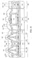
- FIG. 2 shows an organic electroluminescent device with compensation device in accordance with an embodiment of the invention.
- the organic electroluminescent device includes a pixel element 20.
- an organic electroluminescent device 202 is operated by a switch device 206, such as switch integrated circuit(IC) or switch transistor, and a driving device 204 coupling to a power line Vp, also referred to as a driving integrated circuit, driving IC, in which current passing through the driving device 204 is controlled to determine illumination of the organic electroluminescent element 202.
- the switch device 206 is controlled by a column data line 220 and a row scan line 230.
- a capacitor 208 can be coupled to a gate electrode of the driving device 204, in which the capacitor 208 further couples to a photo sensor 210, such as a thin film transistor.
- the photo sensor 210 is a top gate transistor. Voltage of the capacitor 208 is adjusted to control the current passing through the driving device 204 according to illumination of the organic electroluminescent element 202 detected by the photo sensor 210, thus, illumination of the organic electroluminescent element 202 is changed for compensation.
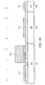
- FIG. 3L shows a cross-sectional view of a pixel element 20 of an organic electroluminescent device of an embodiment of the present invention.
- FIG. 3A ⁇ FIG. 3L show an intermediate cross sections of a pixel element 20 of an organic electroluminescent device with compensation device in accordance with an embodiment of the invention.
- a substrate 302 comprising a control area 304, a sensitive area 306 and a capacitor area 308 is provided, and a buffer layer 310 is formed on the substrate 302.
- the buffer layer 310 can comprise silicon oxide, silicon nitride, silicon oxynitride or a combination thereof, and can be a stack of a silicon oxide layer and a silicon nitride layer.
- thickness of the silicon nitride layer can be about 350 ⁇ 650 ⁇
- thickness of the silicon oxide layer can be about 1000 ⁇ 1600 ⁇ .
- a conductive layer (not shown) is formed on the buffer layer 310.
- the conductive layer can be polysilicon, and formed by for example the following steps.
- An amorphous silicon layer is first formed by deposition with chemical vapor deposition and then crystallized or annealed with excimer laser (ELA) to be transferred to polysilicon.
- the conductive layer is then defined by conventional lithography and etching to form a first active layer 312 and a second active layer 314 overlying the control area 304 of the substrate 302, a photo sensor active layer 316 overlying the sensitive area 306 of the substrate 302, and a bottom electrode layer 318 overlying the capacitor area 308 of the substrate 302. Due to excimer laser annealing, the first active layer 312, the second active layer 312 and the photo sensor active layer 316 are polysilicon, having higher electron transferring speed.
- the second active layer 314 is covered by a photoresist layer 320 to channel dope dopant into the first active layer 312, in which the dopant thereof can comprise B+, and the dosage is typically about 0 ⁇ 1E13/cm 2 .
- channel regions 322 and 324 of the first active layer 312 and the photo sensor active layer 316 are covered by another photoresist layer 330, implanting N+ ions 321 into the first active layer 312 and the photo sensor active layer 316 to form a source 332, a drain 334 and a channel 322 therebetween of a n type transistor, and another source 336, drain 338 and channel 324 therebetween of a photo sensor transistor.
- the N+ ions may comprise phosphorous, and the dosage is preferably about 1E14 ⁇ 1E16cm 2 .
- the bottom electrode layer 318 is n-doped.
- a gate dielectric layer 340 for example silicon oxide, silicon nitride, silicon oxynitride, a combination thereof, a stack layer thereof or other high K dielectric material, is blanketly deposited on the first active layer 312 and the second active layer 314 overlying the control area 304, the photo sensor active layer 316 overlying the sensitive area 306, and the bottom electrode layer 318 overlying the capacitor area 308, in which the gate dielectric layer 340 serves as a capacitor dielectric layer in the capacitor area 308.
- a gate dielectric layer 340 for example silicon oxide, silicon nitride, silicon oxynitride, a combination thereof, a stack layer thereof or other high K dielectric material
- a gate conductive layer (not shown), for example doped polysilicon or metal, is formed on the gate dielectric layer 340.
- the gate conductive layer can be Mo and about 1500 ⁇ ⁇ 2500 ⁇ thick.
- the gate conductive layer is patterned by conventional lithography and etching to form an n type transistor gate 342 overlying the first active layer 312, a p type transistor gate 344 overlying the second active layer 314, and a top electrode layer 346 overlying the capacitor area 308.
- a photo sensor LDD mask layer 348 such as photoresist, are formed on the channel region 324 of the photo sensor active layer 316, wherein width of the photo sensor LDD mask layer 348 is less than the channel region 324.
- a doping step for example ion implantation, is performed to form lightly doped source/drain (LDD) 350 adjacent to opposite sides of the channel region 322 of the first active layer 312 of n type transistor, another lightly doped source/drain (LDD) 352 adjacent to opposite sides of the channel region 324 of the photo sensor active layer 316, and a source 343, drain 345 and channel 341 of the p type transistor.
- LDD lightly doped source/drain
- LDD lightly doped source/drain
- the photo sensor LDD mask layer 348 is removed, and then a dielectric layer 354 is blanketly deposited on the gate dielectric layer 340, the n type transistor gate 342, the p type transistor gate 344, and the top electrode 346 overlying the capacitor area 308.
- a dielectric layer 354 is blanketly deposited on the gate dielectric layer 340, the n type transistor gate 342, the p type transistor gate 344, and the top electrode 346 overlying the capacitor area 308.
- Combination of the gate dielectric layer 340 and the dielectric layer 354 overlying the sensitive area 306 serves as a photo sensor gate dielectric layer of the photo sensor of the organic electroluminescent device.
- Thickness and composition of the dielectric layer 354 can be determined according to product spec or process window.
- the dielectric layer 354 may include silicon dioxide, silicon nitride, silicon oxynitride, polyimide, spin-on-glass (SOG), fluoride-doped silicate glass (FSG) and/or other materials.
- the dielectric layer 354 is a stack layer of silicon oxide layer and silicon nitride layer.
- the silicon oxide layer can be about 1500 ⁇ 2500 ⁇ thick
- the silicon nitride layer can be about 2500 ⁇ 3500 ⁇ thick.
- a photo sensor gate 356 is formed on the dielectric layer 354 overlying the sensitive area 306.
- the photo sensor 210 as shown in FIG. 2 is formed.
- the photo sensor 210 can be a transistor, for example, a top gate transistor.
- the photo sensor gate 356 can be transparent for allowing passage of light to generate current of the photo sensor.
- the photo sensor gate 356 comprises indium tin oxide, ITO and/or indium zinc oxide, IZO.
- a first passivation layer 358 such as silicon nitride, is formed on the photo sensor gate 356 and the dielectric layer 354 for protection.
- the first passivation layer 358, the dielectric layer 354 and the gate dielectric layer 340 are patterned by conventional lithography and etching to form openings 360 exposing the first active layer 312, the second active layer 314, the photo sensor active layer 316, the n type transistor gate 342, the p type transistor gate 344 and/or the photo sensor gate 356 for connection to metal lines in subsequent processes.
- a metal layer (not shown) is blanketly deposited, and then patterned by conventional photolithography and etching to form conductive contacts 362 in the openings 360.
- the second passivation layer 364 can be about 2500 ⁇ 3500 ⁇ thick.
- the second passivation layer 364 is patterned to form openings, exposing at least one of the conductive contacts 362.
- a pixel electrode layer 366 (serving as an anode), for example indium tin oxide (ITO), is formed on the second passivation layer 364, electrically connecting the conductive contacts 362.
- a pixel definition layer 368 for example organic or oxide, is formed on a portion of the second passivation layer 364 and the pixel electrode layer 366 by deposition and patterning thereafter. Specifically, the pixel definition layer 368 exposes a portion of or the entire photo sensor.
- an organic light emitting layer (OLED layer) 370 is formed overlying the pixel electrode layer 366 and the pixel definition layer 368.
- the organic light emitting layer disposed overlying the pixel electrode layer 366 (also referred to as an anode layer, or a first OLED electrode) comprises a hole-injection layer, a hole-transport layer, an organic luminescent material layer, an electron-transport layer, and an electron- injection layer sequentially.
- the anode layer can be indium tin oxide (In2O3:Sn, ITO) which has advantages of facile etching, low film-formation temperature and low resistance.
- an electron and a hole passing through the electron-transport layer and the hole-transport layer respectively enter the organic luminescent material layer to combine as an exciton and then release energy to return to ground state.
- the released energy presents different colors of light including red (R), green (G) and blue (B).
- a cathode layer 372 is formed on the organic light emitting layer 370.
- the cathode layer 372 can be a reflective layer, for example Al, Ag or other suitable material with high reflectivity.
- the pixel electrode layer 366, the organic light emitting layer 370, and the cathode layer 372 constitute the organic electroluminescent element (OLED element) 202 as shown in FIG. 2.
- OLED element organic electroluminescent element
- the photo sensor active layer 316 preferably polysilicon and comprising source 336, drain 338 and channel 324, the dielectric layer 354 and the photo sensor gate 356 thereon constitute a photo TFT sensor 210.
- the p type transistor 204 can act as a driving device and the n type transistor 206 can act as a switch device.
- Photo current is generated in the photo sensor 210. The level of photo current is depending on the brightness of the OLED element 202. Consequently, voltage of a capacitor 208 coupled to the driving device 204 is adjusted to control the current passing through the driving device 204 according to illumination of the organic electroluminescent element 202 detected by the photo sensor 210.
- illumination of the organic electroluminescent element 202 is changed to compensation. Therefore, after aging, brightness uniformity of the OLED element can be improved by such internal compensation.
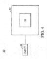
- a pixel element such as the pixel element 20 shown in FIG. 2 or FIG. 3L
- a display panel in this case, display panel 30
- the display panel can form a portion of a variety of electronic devices (in this case, electronic device 50).
- the electronic device 50 comprises the OLED panel 30 and an input unit 40.
- the input unit 40 is operatively coupled to the OLED panel 30 and provides input signals (e.g., an image signal) to the panel 30 to generate images.
- the electronic device can be a mobile phone, digital camera, PDA (personal digital assistant), notebook computer, desktop computer, television, car display, or portable DVD player, for example.
Landscapes
- Engineering & Computer Science (AREA)
- Microelectronics & Electronic Packaging (AREA)
- Manufacturing & Machinery (AREA)
- Electroluminescent Light Sources (AREA)
Abstract
An organic electroluminescent device is disclosed. A substrate comprises a control area and a sensitive area. A switch device and a driving device are disposed overlying the control area. A photo sensor is disposed overlying the sensitive area, wherein the photo sensor is a thin film transistor. An OLED element is disposed in the sensitive area and illuminating to the photo sensor. A capacitor coupled to the photo sensor and the driving device. A photo current corresponding to a brightness of the OLED element is generated by the photo sensor responsive to the OLED element illuminating the photo sensor such that a the voltage of the capacitor is adjusted by the photo current to control the current passing through the driving device, thus changing the illumination of the OLED element.
Description
- The present invention relates to an organic electroluminescent device and fabrication methods thereof.
- Organic electroluminescent devices are also known as organic light emitting diodes (OLED). The OLED luminescent principle applies a voltage to organic molecular material or polymer material, and the device emits light. Due to self emission characteristics of the OLED, dot matrix type displays with light weight, slim profile, high contrast, low power consumption, high resolution, fast response time, no need for backlighting, and wide viewing angle can be obtained. Possible display parameters range from 4mm microdisplay to 100 inch outdoor billboards makes it a preferred type of flat panel display (FPD). If the OLED luminescent efficiency is over 100Lm/W, it can replace conventional lighting.
- Referring to FIG. 1, an organic electroluminescent device is operated by a
switch transistor 102, and adriving transistor 104 coupling to a power line Vp. Organicelectroluminescent devices 106, however, suffer from non-uniform brightness between pixels. Specifically brightness is decayed when the organicelectroluminescent device 106 is operated for a long period. - These and other problems are generally solved or circumvented, and technical advantages are generally achieved, by preferred illustrative embodiments of the present invention, which provide an organic electroluminescent device.
- An embodiment of the invention provides an organic electroluminescent device. A substrate comprises a control area and a sensitive area. A switch device and a driving device are disposed overlying the control area. A photo sensor is disposed overlying the sensitive area, wherein the photo sensor is a thin film transistor. An OLED element is disposed in the sensitive area and illuminates the photo sensor. A capacitor coupled to the photo diode and the driving device. A photo current corresponding to a brightness of the OLED element is generated by the photo sensor responsive to the OLED element illuminating the photo sensor such that a the voltage of the capacitor is adjusted by the photo current to control the current passing through the driving device, thus changing the illumination of the OLED element.
- According to one embodiment of the present invention, the switch device, the driving device and the photo sensor are top gate transistors.
- According to another embodiment of the present invention, the switch device, the driving device, and the photo sensor have active layers of the same layer.
- An embodiment of the invention further provides a method for forming an organic electroluminescent device. A substrate, comprising a control area and a sensitive area is provided. An active layer is formed overlying the control area and the sensitive area of the substrate. A gate dielectric layer is formed overlying the active layer and the sensitive area of the substrate. A conductive layer is formed on the gate dielectric layer. The conductive layer is patterned to form first and second gates in the control area. A dielectric layer is formed at least covering the first gate, the second gate and the gate dielectric layer. A photo sensor gate is formed on the dielectric layer overlying the sensitive area. An OLED element is formed overlying a portion of the control area and the sensitive area.
- The invention can be more fully understood by reading the subsequent detailed description and examples with references made to the accompanying drawings, wherein:
- FIG. 1 shows a conventional circuit diagram of an organic electroluminescent device.
- FIG. 2 shows an organic electroluminescent device with compensation device in accordance with an embodiment of the invention.
- FIG. 3A~FIG. 3L shows an intermediate cross section of an organic electroluminescent device with compensation device in accordance with an embodiment of the invention.
- Fig. 4 shows a pixel element incorporated into an electronic device.
- Embodiments of the invention, which provides an organic electroluminescent device, will be described in greater detail by referring to the drawings that accompany the invention. It is noted that in the accompanying drawings, like and/or corresponding elements are referred to by like reference numerals. The following description discloses the best-contemplated mode of carrying out the invention. This description is made for the purpose of illustrating the general principles of the invention and should not be taken in a limiting sense. The scope of the invention is best determined by reference to the appended claims.
- In this specification, expressions such as "overlying the substrate", "above the layer", or "on the film" simply denote a relative positional relationship with respect to the surface of a base layer, regardless of the existence of intermediate layers. Accordingly, these expressions may indicate not only the direct contact of layers, but also, a non-contact state of one or more laminated layers.
- FIG. 2 shows an organic electroluminescent device with compensation device in accordance with an embodiment of the invention. Referring to FIG. 2, the organic electroluminescent device includes a
pixel element 20. In thepixel element 20, an organicelectroluminescent device 202 is operated by aswitch device 206, such as switch integrated circuit(IC) or switch transistor, and adriving device 204 coupling to a power line Vp, also referred to as a driving integrated circuit, driving IC, in which current passing through thedriving device 204 is controlled to determine illumination of the organicelectroluminescent element 202. Theswitch device 206 is controlled by acolumn data line 220 and arow scan line 230. In an embodiment of the invention, acapacitor 208 can be coupled to a gate electrode of thedriving device 204, in which thecapacitor 208 further couples to aphoto sensor 210, such as a thin film transistor. In an embodiment of the invention, thephoto sensor 210 is a top gate transistor. Voltage of thecapacitor 208 is adjusted to control the current passing through thedriving device 204 according to illumination of the organicelectroluminescent element 202 detected by thephoto sensor 210, thus, illumination of the organicelectroluminescent element 202 is changed for compensation. - FIG. 3L shows a cross-sectional view of a
pixel element 20 of an organic electroluminescent device of an embodiment of the present invention. FIG. 3A~FIG. 3L show an intermediate cross sections of apixel element 20 of an organic electroluminescent device with compensation device in accordance with an embodiment of the invention. Referring to FIG. 3A, asubstrate 302 comprising acontrol area 304, asensitive area 306 and acapacitor area 308 is provided, and abuffer layer 310 is formed on thesubstrate 302. Thebuffer layer 310 can comprise silicon oxide, silicon nitride, silicon oxynitride or a combination thereof, and can be a stack of a silicon oxide layer and a silicon nitride layer. In an embodiment of the invention, thickness of the silicon nitride layer can be about 350Å~650Å, and thickness of the silicon oxide layer can be about 1000Å~1600Å. - Next, a conductive layer (not shown) is formed on the
buffer layer 310. The conductive layer can be polysilicon, and formed by for example the following steps. An amorphous silicon layer is first formed by deposition with chemical vapor deposition and then crystallized or annealed with excimer laser (ELA) to be transferred to polysilicon. The conductive layer is then defined by conventional lithography and etching to form a firstactive layer 312 and a secondactive layer 314 overlying thecontrol area 304 of thesubstrate 302, a photo sensoractive layer 316 overlying thesensitive area 306 of thesubstrate 302, and abottom electrode layer 318 overlying thecapacitor area 308 of thesubstrate 302. Due to excimer laser annealing, the firstactive layer 312, the secondactive layer 312 and the photo sensoractive layer 316 are polysilicon, having higher electron transferring speed. - Referring to FIG. 3B, the second
active layer 314 is covered by aphotoresist layer 320 to channel dope dopant into the firstactive layer 312, in which the dopant thereof can comprise B+, and the dosage is typically about 0~1E13/cm2. Referring to FIG. 3C,channel regions active layer 312 and the photo sensoractive layer 316 are covered by anotherphotoresist layer 330, implantingN+ ions 321 into the firstactive layer 312 and the photo sensoractive layer 316 to form asource 332, adrain 334 and achannel 322 therebetween of a n type transistor, and anothersource 336, drain 338 andchannel 324 therebetween of a photo sensor transistor. In an embodiment of the invention, the N+ ions may comprise phosphorous, and the dosage is preferably about 1E14~1E16cm2. Also, thebottom electrode layer 318 is n-doped. - Referring to FIG. 3D, the photoresist layers 330 are removed, and a
gate dielectric layer 340, for example silicon oxide, silicon nitride, silicon oxynitride, a combination thereof, a stack layer thereof or other high K dielectric material, is blanketly deposited on the firstactive layer 312 and the secondactive layer 314 overlying thecontrol area 304, the photo sensoractive layer 316 overlying thesensitive area 306, and thebottom electrode layer 318 overlying thecapacitor area 308, in which thegate dielectric layer 340 serves as a capacitor dielectric layer in thecapacitor area 308. - Referring to FIG. 3E, a gate conductive layer (not shown), for example doped polysilicon or metal, is formed on the
gate dielectric layer 340. In an embodiment of the invention, the gate conductive layer can be Mo and about 1500Å ~2500Å thick. Next, the gate conductive layer is patterned by conventional lithography and etching to form an ntype transistor gate 342 overlying the firstactive layer 312, a ptype transistor gate 344 overlying the secondactive layer 314, and atop electrode layer 346 overlying thecapacitor area 308. Thereafter, a photo sensorLDD mask layer 348, such as photoresist, are formed on thechannel region 324 of the photo sensoractive layer 316, wherein width of the photo sensorLDD mask layer 348 is less than thechannel region 324. - Subsequent to formation of the
gates mask 348, a doping step, for example ion implantation, is performed to form lightly doped source/drain (LDD) 350 adjacent to opposite sides of thechannel region 322 of the firstactive layer 312 of n type transistor, another lightly doped source/drain (LDD) 352 adjacent to opposite sides of thechannel region 324 of the photo sensoractive layer 316, and asource 343, drain 345 andchannel 341 of the p type transistor. Thus, theswitch device 206 of n type and thedriving device 204 of p type as shown in FIG. 2 are formed in thecontrol area 304. - Next, referring to FIG. 3F, the photo sensor
LDD mask layer 348 is removed, and then adielectric layer 354 is blanketly deposited on thegate dielectric layer 340, the ntype transistor gate 342, the ptype transistor gate 344, and thetop electrode 346 overlying thecapacitor area 308. Combination of thegate dielectric layer 340 and thedielectric layer 354 overlying thesensitive area 306 serves as a photo sensor gate dielectric layer of the photo sensor of the organic electroluminescent device. - Thickness and composition of the
dielectric layer 354 can be determined according to product spec or process window. Thedielectric layer 354 may include silicon dioxide, silicon nitride, silicon oxynitride, polyimide, spin-on-glass (SOG), fluoride-doped silicate glass (FSG) and/or other materials. In an embodiment of the invention, thedielectric layer 354 is a stack layer of silicon oxide layer and silicon nitride layer. For example, the silicon oxide layer can be about 1500~2500Å thick, and the silicon nitride layer can be about 2500~3500Å thick. Next, aphoto sensor gate 356 is formed on thedielectric layer 354 overlying thesensitive area 306. Thus, thephoto sensor 210 as shown in FIG. 2 is formed. In this embodiment, thephoto sensor 210 can be a transistor, for example, a top gate transistor. - The
photo sensor gate 356 can be transparent for allowing passage of light to generate current of the photo sensor. For example, thephoto sensor gate 356 comprises indium tin oxide, ITO and/or indium zinc oxide, IZO. Thereafter, afirst passivation layer 358, such as silicon nitride, is formed on thephoto sensor gate 356 and thedielectric layer 354 for protection. - Referring to FIG. 3G, the
first passivation layer 358, thedielectric layer 354 and thegate dielectric layer 340 are patterned by conventional lithography and etching to formopenings 360 exposing the firstactive layer 312, the secondactive layer 314, the photo sensoractive layer 316, the ntype transistor gate 342, the ptype transistor gate 344 and/or thephoto sensor gate 356 for connection to metal lines in subsequent processes. - Next, referring to FIG. 3H, a metal layer (not shown) is blanketly deposited, and then patterned by conventional photolithography and etching to form
conductive contacts 362 in theopenings 360. - Referring to FIG. 3I, a
second passivation layer 364, for example silicon nitride, is formed on theconductive contacts 362 and thefirst passivation layer 358 for passivation thereof. For example, thesecond passivation layer 364 can be about 2500Å~3500Å thick. Referring to FIG. 3J, thesecond passivation layer 364 is patterned to form openings, exposing at least one of theconductive contacts 362. - Next, in FIG. 3J, a pixel electrode layer 366 (serving as an anode), for example indium tin oxide (ITO), is formed on the
second passivation layer 364, electrically connecting theconductive contacts 362. Next, in FIG.3K, apixel definition layer 368, for example organic or oxide, is formed on a portion of thesecond passivation layer 364 and thepixel electrode layer 366 by deposition and patterning thereafter. Specifically, thepixel definition layer 368 exposes a portion of or the entire photo sensor. - Referring to FIG. 3L, an organic light emitting layer (OLED layer) 370 is formed overlying the
pixel electrode layer 366 and thepixel definition layer 368. In an embodiment of the invention, the organic light emitting layer disposed overlying the pixel electrode layer 366 (also referred to as an anode layer, or a first OLED electrode) comprises a hole-injection layer, a hole-transport layer, an organic luminescent material layer, an electron-transport layer, and an electron- injection layer sequentially. The anode layer can be indium tin oxide (In2O3:Sn, ITO) which has advantages of facile etching, low film-formation temperature and low resistance. When a bias voltage is applied to theOLED layer 370, an electron and a hole passing through the electron-transport layer and the hole-transport layer respectively enter the organic luminescent material layer to combine as an exciton and then release energy to return to ground state. Particularly, depending on the nature of the organic luminescent material, the released energy presents different colors of light including red (R), green (G) and blue (B). - Next, a
cathode layer 372 is formed on the organiclight emitting layer 370. Thecathode layer 372 can be a reflective layer, for example Al, Ag or other suitable material with high reflectivity. Thus, thepixel electrode layer 366, the organiclight emitting layer 370, and thecathode layer 372 constitute the organic electroluminescent element (OLED element) 202 as shown in FIG. 2. A bottom emission organic electroluminescent device is thus formed. - As shown in FIG. 2 and 3L, in the described preferred embodiments of the invention, the photo sensor
active layer 316, preferably polysilicon and comprisingsource 336, drain 338 andchannel 324, thedielectric layer 354 and thephoto sensor gate 356 thereon constitute aphoto TFT sensor 210. Thep type transistor 204 can act as a driving device and then type transistor 206 can act as a switch device. Photo current is generated in thephoto sensor 210. The level of photo current is depending on the brightness of theOLED element 202. Consequently, voltage of acapacitor 208 coupled to thedriving device 204 is adjusted to control the current passing through thedriving device 204 according to illumination of theorganic electroluminescent element 202 detected by thephoto sensor 210. Thus, illumination of theorganic electroluminescent element 202 is changed to compensation. Therefore, after aging, brightness uniformity of the OLED element can be improved by such internal compensation. - In this regard, Fig. 4 shows that a pixel element, such as the
pixel element 20 shown in FIG. 2 or FIG. 3L, can be incorporated into a display panel (in this case, display panel 30) that can be an OLED panel. The display panel can form a portion of a variety of electronic devices (in this case, electronic device 50). Generally, theelectronic device 50 comprises theOLED panel 30 and aninput unit 40. Further, theinput unit 40 is operatively coupled to theOLED panel 30 and provides input signals (e.g., an image signal) to thepanel 30 to generate images. The electronic device can be a mobile phone, digital camera, PDA (personal digital assistant), notebook computer, desktop computer, television, car display, or portable DVD player, for example. - While the invention has been described by way of example and in terms of the preferred embodiment, it is to be understood that the invention is not limited thereto. To the contrary, it is intended to cover various modifications and similar arrangements (as would be apparent to those skilled in the art). Therefore, the scope of the appended claims should be accorded the broadest interpretation so as to encompass all such modifications and similar arrangements.
Claims (14)
- An organic electroluminescent device, comprising:a pixel element comprising:wherein a photo current corresponding to a brightness of the OLED element is generated by the photo sensor responsive to the OLED element illuminating the photo sensor such that a the voltage of the capacitor is adjusted by the photo current to control the current passing through the driving device, thus changing the illumination of the OLED element.a substrate, comprising a control area and a sensitive area;a switch device and a driving device overlying the control area;a photo sensor overlying the sensitive area, wherein the photo sensor is a thin film transistor; andan OLED element disposed in the sensitive area and illuminating to the photo sensor; anda capacitor coupled to the photo sensor and the driving device;
- The organic electroluminescent device as claimed in claim 1, wherein the switch device and the driving device are top gate transistors.
- The organic electroluminescent device as claimed in claim 1 or 2, wherein the photo sensor is a polysilicon thin film transistor.
- The organic electroluminescent device as claimed in claim 3, wherein the polysilicon thin film transistor comprises:a buffer layer overlying the substrate;a photo sensor active layer, comprising a source, a drain and a channel therebetween, overlying the buffer layer;a dielectric layer overlying the photo sensor active layer; anda photo sensor gate overlying the dielectric layer, wherein the photo sensor gate is transparent.
- The organic electroluminescent device as claimed in claim 4, wherein the photo sensor active layer comprises polysilicon, and the photo sensor gate comprises indium tin oxide, ITO or indium zinc oxide, IZO.
- The organic electroluminescent device as claimed in any of the preceding claims, wherein the switch device has a first active layer, the driving device has a second active layer, and the photo sensor active layer, the first active layer and the second active layer are formed of the same layer.
- The organic electroluminescent device as claimed in any of the preceding claims, further comprising:a first active layer disposed in the switch device;a second active layer disposed in the driving device;a photo sensor active layer disposed in the photo sensor;a gate dielectric layer disposed overlying the first, the second active layers and the photo sensor active layer;first and second gates disposed on the gate dielectric layer overlying the control area, wherein the first gate is in the switch device, and the second gate is in the driving device;a dielectric layer at least covering the first gate, the second gate, and the gate dielectric layer; anda photo sensor gate overlying the dielectric layer in the sensitive area.
- The organic electroluminescent device as claimed in claim 7, wherein the dielectric layer and the gate dielectric layer further comprise a plurality of openings, exposing the first and second gates and a portion of the first and second active layers, and the openings are filled with conductive contacts.
- The organic electroluminescent device as claimed in claim 7 or 8, further comprising:a passivation layer disposed overlying the conductive contacts and the dielectric layer;a first OLED electrode overlying the planarization layer;an organic light emitting layer disposed on the first electrode; anda second OLED electrode disposed overlying the organic light emitting layer, wherein the first electrode, the organic light emitting layer and the second electrode constitutes the OLED element.
- The organic electroluminescent device as claimed in any of the preceding claims, further comprising:a display panel, wherein the pixel element is arranged in an array of pixel elements of the display panel.
- The organic electroluminescent device as claimed in claim 10, further comprising an electronic device, wherein the electronic device comprises:the display panel; andan input unit coupled to the display panel and operative to provide input to the display panel such that they display panel displays images.
- The organic electroluminescent device as claimed in claim 11, wherein the electronic device is a mobile phone, digital camera, PDA (personal digital assistant), notebook computer, desktop computer, television, car display, or portable DVD player.
- An organic electroluminescent device, comprising:a pixel element comprising:wherein a photo current corresponding to a brightness of the OLED element is generated by the photo sensor responsive to the OLED element illuminating the photo sensor such that a the voltage of the capacitor is adjusted by the photo current to control the current passing through the driving device, thus changing the illumination of the OLED element,a substrate, comprising a control area and a sensitive area;a switch device and a driving device overlying the control area;a photo sensor overlying the sensitive area; andan OLED element disposed in the sensitive area and illuminating to the photo sensor; anda capacitor coupled to the photo photo sensor and the driving device;
wherein the switch device, the driving device and the photo sensor are top gate transistors,
wherein the switch device, the driving device, and the photo sensor have active layers of the same layer. - A method for forming an organic electroluminescent device, comprising:providing a substrate, comprising a control area and a sensitive area;forming an active layer overlying the control area and the sensitive area of the substrate;patterning the active layer to form first and second active layers in the control area, and a photo sensor active layer in the sensitive area;forming a gate dielectric layer overlying the active layer and the sensitive area of the substrate;forming a conductive layer on the gate dielectric layer;patterning the conductive layer to form first and second gates in the control area;forming a dielectric layer at least covering the first gate, the second gate and the gate dielectric layer;forming a photo sensor gate on the dielectric layer overlying the sensitive area; andforming an OLED element overlying a portion of the control area and the sensitive area.
Priority Applications (1)
| Application Number | Priority Date | Filing Date | Title |
|---|---|---|---|
| EP06112123A EP1840971A1 (en) | 2006-03-31 | 2006-03-31 | Organic electroluminescent device and fabrication methods thereof |
Applications Claiming Priority (1)
| Application Number | Priority Date | Filing Date | Title |
|---|---|---|---|
| EP06112123A EP1840971A1 (en) | 2006-03-31 | 2006-03-31 | Organic electroluminescent device and fabrication methods thereof |
Publications (1)
| Publication Number | Publication Date |
|---|---|
| EP1840971A1 true EP1840971A1 (en) | 2007-10-03 |
Family
ID=36729960
Family Applications (1)
| Application Number | Title | Priority Date | Filing Date |
|---|---|---|---|
| EP06112123A Withdrawn EP1840971A1 (en) | 2006-03-31 | 2006-03-31 | Organic electroluminescent device and fabrication methods thereof |
Country Status (1)
| Country | Link |
|---|---|
| EP (1) | EP1840971A1 (en) |
Cited By (4)
| Publication number | Priority date | Publication date | Assignee | Title |
|---|---|---|---|---|
| CN101650914A (en) * | 2009-06-17 | 2010-02-17 | 北京巨数数字技术开发有限公司 | Point-to-point correction system |
| WO2014205982A1 (en) * | 2013-06-28 | 2014-12-31 | 京东方科技集团股份有限公司 | Display panel |
| CN108008228A (en) * | 2018-01-31 | 2018-05-08 | 吉林大学 | A kind of chip-Size semiconductor gas sensor aging equipment |
| CN113892133A (en) * | 2019-05-31 | 2022-01-04 | 华为技术有限公司 | Pixel circuit and pixel control method |
Citations (5)
| Publication number | Priority date | Publication date | Assignee | Title |
|---|---|---|---|---|
| US20010028060A1 (en) * | 2000-01-11 | 2001-10-11 | Shunpei Yamazaki | Semiconductor display device |
| US6489631B2 (en) * | 2000-06-20 | 2002-12-03 | Koninklijke Phillips Electronics N.V. | Light-emitting matrix array display devices with light sensing elements |
| WO2005093838A1 (en) * | 2004-03-24 | 2005-10-06 | Koninklijke Philips Electronics N.V. | Electroluminescent display devices |
| US20050248264A1 (en) * | 2004-05-05 | 2005-11-10 | Eastman Kodak Company | OLED display with composite photosensor |
| US20060030084A1 (en) * | 2002-08-24 | 2006-02-09 | Koninklijke Philips Electronics, N.V. | Manufacture of electronic devices comprising thin-film circuit elements |
-
2006
- 2006-03-31 EP EP06112123A patent/EP1840971A1/en not_active Withdrawn
Patent Citations (5)
| Publication number | Priority date | Publication date | Assignee | Title |
|---|---|---|---|---|
| US20010028060A1 (en) * | 2000-01-11 | 2001-10-11 | Shunpei Yamazaki | Semiconductor display device |
| US6489631B2 (en) * | 2000-06-20 | 2002-12-03 | Koninklijke Phillips Electronics N.V. | Light-emitting matrix array display devices with light sensing elements |
| US20060030084A1 (en) * | 2002-08-24 | 2006-02-09 | Koninklijke Philips Electronics, N.V. | Manufacture of electronic devices comprising thin-film circuit elements |
| WO2005093838A1 (en) * | 2004-03-24 | 2005-10-06 | Koninklijke Philips Electronics N.V. | Electroluminescent display devices |
| US20050248264A1 (en) * | 2004-05-05 | 2005-11-10 | Eastman Kodak Company | OLED display with composite photosensor |
Non-Patent Citations (1)
| Title |
|---|
| D. FISH, N. YOUNG, S. DEANE, A. STEER, D. GEORGE, A. GIRALDO, H. LIFKA, O. GIELKENS, W. OEPTS: "Optical Feedback for AMOLED display Compensation using LTPS and a-Si:H Technologies", DIG. TECH. PAP. SID INT. SYMP.; DIGEST OF TECHNICAL PAPERS - SID INTERNATIONAL SYMPOSIUM; 2005 SID INTERNATIONAL SYMPOSIUM - DIGEST OF TECHNICAL PAPERS 2005, vol. 38, no. 1, 9 May 2005 (2005-05-09), ENGINEERING INFORMATION, INC., NEW YORK, NY, US, pages 1340 - 1343, XP002394239 * |
Cited By (6)
| Publication number | Priority date | Publication date | Assignee | Title |
|---|---|---|---|---|
| CN101650914A (en) * | 2009-06-17 | 2010-02-17 | 北京巨数数字技术开发有限公司 | Point-to-point correction system |
| CN101650914B (en) * | 2009-06-17 | 2016-01-20 | 北京巨数数字技术开发有限公司 | A kind of point-to-point correction system |
| WO2014205982A1 (en) * | 2013-06-28 | 2014-12-31 | 京东方科技集团股份有限公司 | Display panel |
| CN108008228A (en) * | 2018-01-31 | 2018-05-08 | 吉林大学 | A kind of chip-Size semiconductor gas sensor aging equipment |
| CN113892133A (en) * | 2019-05-31 | 2022-01-04 | 华为技术有限公司 | Pixel circuit and pixel control method |
| US12067936B2 (en) | 2019-05-31 | 2024-08-20 | Huawei Technologies Co., Ltd. | Pixel circuit and pixel control method |
Similar Documents
| Publication | Publication Date | Title |
|---|---|---|
| US7397065B2 (en) | Organic electroluminescent device and fabrication methods thereof | |
| US20070236428A1 (en) | Organic electroluminescent device and fabrication methods thereof | |
| US7449697B2 (en) | Organic electroluminescent devices and fabrication methods thereof | |
| US20070236429A1 (en) | Organic electroluminescent device and fabrication methods thereof | |
| US7790526B2 (en) | System for displaying images and method for fabricating the same | |
| US6515428B1 (en) | Pixel structure an organic light-emitting diode display device and its manufacturing method | |
| US8963137B2 (en) | Organic light-emitting display device and method of fabricating the same | |
| KR100426031B1 (en) | an active matrix organic electroluminescence display and a manufacturing method of the same | |
| US7875889B2 (en) | Active matrix type organic electroluminescent display device and method of manufacturing the same | |
| US7800298B2 (en) | Light-emitting device having a planarized color filter | |
| US20130056784A1 (en) | Organic Light-Emitting Display Device and Method of Fabricating the Same | |
| US8710733B2 (en) | Organic light-emitting display with black matrix | |
| US20050189535A1 (en) | Organic light-emitting device and method of fabricating the same | |
| KR20070004742A (en) | Electroluminescent display devices | |
| CN110972507B (en) | Array substrate, manufacturing method thereof and display device | |
| KR20140084603A (en) | Dual sided emission type Organic electro luminescent device | |
| EP1840971A1 (en) | Organic electroluminescent device and fabrication methods thereof | |
| KR102473069B1 (en) | Display device and manufacturing method thereof | |
| US20080197354A1 (en) | Thin film transistor, an organic light emitting device including the same, and a manufacturing method thereof | |
| EP1837912A1 (en) | Organic electroluminescent device and fabrication methods thereof | |
| EP1852845B1 (en) | Organic electroluminescent device and fabrication methods thereof | |
| US20060043373A1 (en) | Method for manufacturing a pixel array of top emitting OLED | |
| EP1808897A1 (en) | Organic electroluminescent device and fabrication method thereof | |
| KR20030085239A (en) | Active Matrix Organic Electro-Luminescence Display Panel And Method Of Fabricating The Same | |
| US20070241331A1 (en) | Electroluminescent device and methods for fabricating the same |
Legal Events
| Date | Code | Title | Description |
|---|---|---|---|
| PUAI | Public reference made under article 153(3) epc to a published international application that has entered the european phase |
Free format text: ORIGINAL CODE: 0009012 |
|
| AK | Designated contracting states |
Kind code of ref document: A1 Designated state(s): AT BE BG CH CY CZ DE DK EE ES FI FR GB GR HU IE IS IT LI LT LU LV MC NL PL PT RO SE SI SK TR |
|
| AX | Request for extension of the european patent |
Extension state: AL BA HR MK YU |
|
| AKX | Designation fees paid | ||
| STAA | Information on the status of an ep patent application or granted ep patent |
Free format text: STATUS: THE APPLICATION IS DEEMED TO BE WITHDRAWN |
|
| 18D | Application deemed to be withdrawn |
Effective date: 20080404 |
|
| REG | Reference to a national code |
Ref country code: DE Ref legal event code: 8566 |