EP1840952A1 - Devices with microjetted polymer standoffs - Google Patents
Devices with microjetted polymer standoffs Download PDFInfo
- Publication number
- EP1840952A1 EP1840952A1 EP07075207A EP07075207A EP1840952A1 EP 1840952 A1 EP1840952 A1 EP 1840952A1 EP 07075207 A EP07075207 A EP 07075207A EP 07075207 A EP07075207 A EP 07075207A EP 1840952 A1 EP1840952 A1 EP 1840952A1
- Authority
- EP
- European Patent Office
- Prior art keywords
- substrate
- surface mount
- electronic device
- standoffs
- polymeric
- Prior art date
- Legal status (The legal status is an assumption and is not a legal conclusion. Google has not performed a legal analysis and makes no representation as to the accuracy of the status listed.)
- Withdrawn
Links
Images
Classifications
-
- H—ELECTRICITY
- H05—ELECTRIC TECHNIQUES NOT OTHERWISE PROVIDED FOR
- H05K—PRINTED CIRCUITS; CASINGS OR CONSTRUCTIONAL DETAILS OF ELECTRIC APPARATUS; MANUFACTURE OF ASSEMBLAGES OF ELECTRICAL COMPONENTS
- H05K3/00—Apparatus or processes for manufacturing printed circuits
- H05K3/30—Assembling printed circuits with electric components, e.g. with resistors
- H05K3/303—Assembling printed circuits with electric components, e.g. with resistors with surface mounted components
-
- H—ELECTRICITY
- H10—SEMICONDUCTOR DEVICES; ELECTRIC SOLID-STATE DEVICES NOT OTHERWISE PROVIDED FOR
- H10W—GENERIC PACKAGES, INTERCONNECTIONS, CONNECTORS OR OTHER CONSTRUCTIONAL DETAILS OF DEVICES COVERED BY CLASS H10
- H10W72/00—Interconnections or connectors in packages
- H10W72/30—Die-attach connectors
-
- H—ELECTRICITY
- H10—SEMICONDUCTOR DEVICES; ELECTRIC SOLID-STATE DEVICES NOT OTHERWISE PROVIDED FOR
- H10W—GENERIC PACKAGES, INTERCONNECTIONS, CONNECTORS OR OTHER CONSTRUCTIONAL DETAILS OF DEVICES COVERED BY CLASS H10
- H10W74/00—Encapsulations, e.g. protective coatings
- H10W74/01—Manufacture or treatment
- H10W74/012—Manufacture or treatment of encapsulations on active surfaces of flip-chip devices, e.g. forming underfills
-
- H—ELECTRICITY
- H10—SEMICONDUCTOR DEVICES; ELECTRIC SOLID-STATE DEVICES NOT OTHERWISE PROVIDED FOR
- H10W—GENERIC PACKAGES, INTERCONNECTIONS, CONNECTORS OR OTHER CONSTRUCTIONAL DETAILS OF DEVICES COVERED BY CLASS H10
- H10W74/00—Encapsulations, e.g. protective coatings
- H10W74/10—Encapsulations, e.g. protective coatings characterised by their shape or disposition
- H10W74/111—Encapsulations, e.g. protective coatings characterised by their shape or disposition the semiconductor body being completely enclosed
- H10W74/124—Encapsulations, e.g. protective coatings characterised by their shape or disposition the semiconductor body being completely enclosed the encapsulations having cavities other than that occupied by chips
-
- H—ELECTRICITY
- H10—SEMICONDUCTOR DEVICES; ELECTRIC SOLID-STATE DEVICES NOT OTHERWISE PROVIDED FOR
- H10W—GENERIC PACKAGES, INTERCONNECTIONS, CONNECTORS OR OTHER CONSTRUCTIONAL DETAILS OF DEVICES COVERED BY CLASS H10
- H10W74/00—Encapsulations, e.g. protective coatings
- H10W74/10—Encapsulations, e.g. protective coatings characterised by their shape or disposition
- H10W74/15—Encapsulations, e.g. protective coatings characterised by their shape or disposition on active surfaces of flip-chip devices, e.g. underfills
-
- H—ELECTRICITY
- H05—ELECTRIC TECHNIQUES NOT OTHERWISE PROVIDED FOR
- H05K—PRINTED CIRCUITS; CASINGS OR CONSTRUCTIONAL DETAILS OF ELECTRIC APPARATUS; MANUFACTURE OF ASSEMBLAGES OF ELECTRICAL COMPONENTS
- H05K2201/00—Indexing scheme relating to printed circuits covered by H05K1/00
- H05K2201/09—Shape and layout
- H05K2201/09818—Shape or layout details not covered by a single group of H05K2201/09009 - H05K2201/09809
- H05K2201/09909—Special local insulating pattern, e.g. as dam around component
-
- H—ELECTRICITY
- H05—ELECTRIC TECHNIQUES NOT OTHERWISE PROVIDED FOR
- H05K—PRINTED CIRCUITS; CASINGS OR CONSTRUCTIONAL DETAILS OF ELECTRIC APPARATUS; MANUFACTURE OF ASSEMBLAGES OF ELECTRICAL COMPONENTS
- H05K2201/00—Indexing scheme relating to printed circuits covered by H05K1/00
- H05K2201/10—Details of components or other objects attached to or integrated in a printed circuit board
- H05K2201/10613—Details of electrical connections of non-printed components, e.g. special leads
- H05K2201/10621—Components characterised by their electrical contacts
- H05K2201/10674—Flip chip
-
- H—ELECTRICITY
- H05—ELECTRIC TECHNIQUES NOT OTHERWISE PROVIDED FOR
- H05K—PRINTED CIRCUITS; CASINGS OR CONSTRUCTIONAL DETAILS OF ELECTRIC APPARATUS; MANUFACTURE OF ASSEMBLAGES OF ELECTRICAL COMPONENTS
- H05K2201/00—Indexing scheme relating to printed circuits covered by H05K1/00
- H05K2201/10—Details of components or other objects attached to or integrated in a printed circuit board
- H05K2201/10613—Details of electrical connections of non-printed components, e.g. special leads
- H05K2201/10954—Other details of electrical connections
- H05K2201/10977—Encapsulated connections
-
- H—ELECTRICITY
- H05—ELECTRIC TECHNIQUES NOT OTHERWISE PROVIDED FOR
- H05K—PRINTED CIRCUITS; CASINGS OR CONSTRUCTIONAL DETAILS OF ELECTRIC APPARATUS; MANUFACTURE OF ASSEMBLAGES OF ELECTRICAL COMPONENTS
- H05K2201/00—Indexing scheme relating to printed circuits covered by H05K1/00
- H05K2201/20—Details of printed circuits not provided for in H05K2201/01 - H05K2201/10
- H05K2201/2036—Permanent spacer or stand-off in a printed circuit or printed circuit assembly
-
- H—ELECTRICITY
- H05—ELECTRIC TECHNIQUES NOT OTHERWISE PROVIDED FOR
- H05K—PRINTED CIRCUITS; CASINGS OR CONSTRUCTIONAL DETAILS OF ELECTRIC APPARATUS; MANUFACTURE OF ASSEMBLAGES OF ELECTRICAL COMPONENTS
- H05K2203/00—Indexing scheme relating to apparatus or processes for manufacturing printed circuits covered by H05K3/00
- H05K2203/01—Tools for processing; Objects used during processing
- H05K2203/0104—Tools for processing; Objects used during processing for patterning or coating
- H05K2203/013—Inkjet printing, e.g. for printing insulating material or resist
-
- H—ELECTRICITY
- H05—ELECTRIC TECHNIQUES NOT OTHERWISE PROVIDED FOR
- H05K—PRINTED CIRCUITS; CASINGS OR CONSTRUCTIONAL DETAILS OF ELECTRIC APPARATUS; MANUFACTURE OF ASSEMBLAGES OF ELECTRICAL COMPONENTS
- H05K3/00—Apparatus or processes for manufacturing printed circuits
- H05K3/30—Assembling printed circuits with electric components, e.g. with resistors
- H05K3/32—Assembling printed circuits with electric components, e.g. with resistors electrically connecting electric components or wires to printed circuits
- H05K3/34—Assembling printed circuits with electric components, e.g. with resistors electrically connecting electric components or wires to printed circuits by soldering
- H05K3/341—Surface mounted components
- H05K3/3431—Leadless components
- H05K3/3436—Leadless components having an array of bottom contacts, e.g. pad grid array or ball grid array components
-
- H—ELECTRICITY
- H10—SEMICONDUCTOR DEVICES; ELECTRIC SOLID-STATE DEVICES NOT OTHERWISE PROVIDED FOR
- H10W—GENERIC PACKAGES, INTERCONNECTIONS, CONNECTORS OR OTHER CONSTRUCTIONAL DETAILS OF DEVICES COVERED BY CLASS H10
- H10W72/00—Interconnections or connectors in packages
- H10W72/01—Manufacture or treatment
- H10W72/012—Manufacture or treatment of bump connectors, dummy bumps or thermal bumps
- H10W72/01221—Manufacture or treatment of bump connectors, dummy bumps or thermal bumps using local deposition
- H10W72/01225—Manufacture or treatment of bump connectors, dummy bumps or thermal bumps using local deposition in solid form, e.g. by using a powder or by stud bumping
-
- H—ELECTRICITY
- H10—SEMICONDUCTOR DEVICES; ELECTRIC SOLID-STATE DEVICES NOT OTHERWISE PROVIDED FOR
- H10W—GENERIC PACKAGES, INTERCONNECTIONS, CONNECTORS OR OTHER CONSTRUCTIONAL DETAILS OF DEVICES COVERED BY CLASS H10
- H10W72/00—Interconnections or connectors in packages
- H10W72/071—Connecting or disconnecting
- H10W72/072—Connecting or disconnecting of bump connectors
-
- H—ELECTRICITY
- H10—SEMICONDUCTOR DEVICES; ELECTRIC SOLID-STATE DEVICES NOT OTHERWISE PROVIDED FOR
- H10W—GENERIC PACKAGES, INTERCONNECTIONS, CONNECTORS OR OTHER CONSTRUCTIONAL DETAILS OF DEVICES COVERED BY CLASS H10
- H10W72/00—Interconnections or connectors in packages
- H10W72/071—Connecting or disconnecting
- H10W72/072—Connecting or disconnecting of bump connectors
- H10W72/07221—Aligning
- H10W72/07227—Aligning involving guiding structures, e.g. spacers or supporting members
-
- H—ELECTRICITY
- H10—SEMICONDUCTOR DEVICES; ELECTRIC SOLID-STATE DEVICES NOT OTHERWISE PROVIDED FOR
- H10W—GENERIC PACKAGES, INTERCONNECTIONS, CONNECTORS OR OTHER CONSTRUCTIONAL DETAILS OF DEVICES COVERED BY CLASS H10
- H10W72/00—Interconnections or connectors in packages
- H10W72/071—Connecting or disconnecting
- H10W72/072—Connecting or disconnecting of bump connectors
- H10W72/07231—Techniques
- H10W72/07234—Using a reflow oven
-
- H—ELECTRICITY
- H10—SEMICONDUCTOR DEVICES; ELECTRIC SOLID-STATE DEVICES NOT OTHERWISE PROVIDED FOR
- H10W—GENERIC PACKAGES, INTERCONNECTIONS, CONNECTORS OR OTHER CONSTRUCTIONAL DETAILS OF DEVICES COVERED BY CLASS H10
- H10W72/00—Interconnections or connectors in packages
- H10W72/071—Connecting or disconnecting
- H10W72/072—Connecting or disconnecting of bump connectors
- H10W72/07231—Techniques
- H10W72/07236—Soldering or alloying
-
- H—ELECTRICITY
- H10—SEMICONDUCTOR DEVICES; ELECTRIC SOLID-STATE DEVICES NOT OTHERWISE PROVIDED FOR
- H10W—GENERIC PACKAGES, INTERCONNECTIONS, CONNECTORS OR OTHER CONSTRUCTIONAL DETAILS OF DEVICES COVERED BY CLASS H10
- H10W72/00—Interconnections or connectors in packages
- H10W72/071—Connecting or disconnecting
- H10W72/073—Connecting or disconnecting of die-attach connectors
-
- H—ELECTRICITY
- H10—SEMICONDUCTOR DEVICES; ELECTRIC SOLID-STATE DEVICES NOT OTHERWISE PROVIDED FOR
- H10W—GENERIC PACKAGES, INTERCONNECTIONS, CONNECTORS OR OTHER CONSTRUCTIONAL DETAILS OF DEVICES COVERED BY CLASS H10
- H10W72/00—Interconnections or connectors in packages
- H10W72/20—Bump connectors, e.g. solder bumps or copper pillars; Dummy bumps; Thermal bumps
- H10W72/281—Auxiliary members
- H10W72/285—Alignment aids, e.g. alignment marks
-
- H—ELECTRICITY
- H10—SEMICONDUCTOR DEVICES; ELECTRIC SOLID-STATE DEVICES NOT OTHERWISE PROVIDED FOR
- H10W—GENERIC PACKAGES, INTERCONNECTIONS, CONNECTORS OR OTHER CONSTRUCTIONAL DETAILS OF DEVICES COVERED BY CLASS H10
- H10W72/00—Interconnections or connectors in packages
- H10W72/851—Dispositions of multiple connectors or interconnections
- H10W72/853—On the same surface
- H10W72/856—Bump connectors and die-attach connectors
-
- H—ELECTRICITY
- H10—SEMICONDUCTOR DEVICES; ELECTRIC SOLID-STATE DEVICES NOT OTHERWISE PROVIDED FOR
- H10W—GENERIC PACKAGES, INTERCONNECTIONS, CONNECTORS OR OTHER CONSTRUCTIONAL DETAILS OF DEVICES COVERED BY CLASS H10
- H10W72/00—Interconnections or connectors in packages
- H10W72/90—Bond pads, in general
-
- H—ELECTRICITY
- H10—SEMICONDUCTOR DEVICES; ELECTRIC SOLID-STATE DEVICES NOT OTHERWISE PROVIDED FOR
- H10W—GENERIC PACKAGES, INTERCONNECTIONS, CONNECTORS OR OTHER CONSTRUCTIONAL DETAILS OF DEVICES COVERED BY CLASS H10
- H10W72/00—Interconnections or connectors in packages
- H10W72/90—Bond pads, in general
- H10W72/941—Dispositions of bond pads
- H10W72/9415—Dispositions of bond pads relative to the surface, e.g. recessed, protruding
-
- H—ELECTRICITY
- H10—SEMICONDUCTOR DEVICES; ELECTRIC SOLID-STATE DEVICES NOT OTHERWISE PROVIDED FOR
- H10W—GENERIC PACKAGES, INTERCONNECTIONS, CONNECTORS OR OTHER CONSTRUCTIONAL DETAILS OF DEVICES COVERED BY CLASS H10
- H10W90/00—Package configurations
- H10W90/701—Package configurations characterised by the relative positions of pads or connectors relative to package parts
- H10W90/721—Package configurations characterised by the relative positions of pads or connectors relative to package parts of bump connectors
- H10W90/724—Package configurations characterised by the relative positions of pads or connectors relative to package parts of bump connectors between a chip and a stacked insulating package substrate, interposer or RDL
-
- Y—GENERAL TAGGING OF NEW TECHNOLOGICAL DEVELOPMENTS; GENERAL TAGGING OF CROSS-SECTIONAL TECHNOLOGIES SPANNING OVER SEVERAL SECTIONS OF THE IPC; TECHNICAL SUBJECTS COVERED BY FORMER USPC CROSS-REFERENCE ART COLLECTIONS [XRACs] AND DIGESTS
- Y02—TECHNOLOGIES OR APPLICATIONS FOR MITIGATION OR ADAPTATION AGAINST CLIMATE CHANGE
- Y02P—CLIMATE CHANGE MITIGATION TECHNOLOGIES IN THE PRODUCTION OR PROCESSING OF GOODS
- Y02P70/00—Climate change mitigation technologies in the production process for final industrial or consumer products
- Y02P70/50—Manufacturing or production processes characterised by the final manufactured product
Definitions
- This invention pertains to electronic semiconductor packages and more particularly to electronic semiconductor packages having standoffs between a substrate and an electronic device mounted on the substrate.
- Electronic semiconductor packages are typically comprised of a substrate, such as a printed circuit board, and electronic components or chips that are mounted on the substrate and electrically connected to conductors on the substrate.
- a substrate such as a printed circuit board
- electronic components or chips that are mounted on the substrate and electrically connected to conductors on the substrate.
- so-called "surface mount” or lead-less electronic components are often preferred. These surface mount electronic components are characterized by the absence of electrical lead wires. Instead, electrical connections between the surface component and the substrate are achieved by a soldered joint located between a terminal on the component and a mounting pad on the substrate and in direct contact with the terminal and mounting pad. Examples of surface mount electronic components include flip chips, ball grid arrays, chip-scale packages, diodes, inductors, capacitors, resistors, and varisters.
- a flexible, stainless steel spring spacer has been retained between the underside of a surface mount electronic component and the upper surface of a printed circuit board on which the component is mounted in order to reduce pressure on solder joints when a heat sink is mechanically clamped to the electronic package.
- Attempts to maintain an appropriate gap between a surface mount component and a substrate on which the electronic component is mounted have included the use of particulate conductive stand-off members distributed in a solder joint.
- the stand-off members are comprised of metal alloy having a higher melting temperature than the solder.
- the invention provides an electronic package comprising a substrate having electrically conductive pathways and at least one conductive mounting pad, a surface mount electronic device having at least one terminal, and a plurality of polymeric standoffs adhered to at least one of the underside of the surface mount electronic device or an upper surface of the substrate to maintain a desired gap between the underside of the surface mount electronic device and the upper surface of the substrate.
- At least one solder joint electrically and mechanically connects the terminal of the surface mount device to the mounting pad of the substrate.
- the polymeric standoffs are preferably configured and arranged between the underside of the surface mount electronic device and the substrate to prevent collapse of the electronic device during an overmolding operation.
- a process for making an electronic package having a controlled height standoff distance between a surface mount device and a circuit board includes steps of providing a substrate having electrically conductive pathways and at least one conductive mounting pad, providing a surface mount electronic device having at least one terminal, depositing a plurality of polymeric standoffs on, and adhering the plurality of polymeric standoffs to, at least one of the underside of the surface mount electronic device or an upper surface of the substrate, and forming a solder joint to connect the terminal of the surface mount device to the mounting pad of the substrate.
- the polymeric standoffs are preferably configured and arranged on the underside of the surface mount electronic device or the upper surface of the substrate to maintain a desired gap between the underside of the surface mount electronic device and the upper surface of the substrate, and to prevent collapse of the surface mount electronic device during overmolding or encapsulation of the surface mount electronic device. Furthermore, fine-pitched devices would be supported during reflow and this would reduce the risk of shorts developing between adjacent bumps.
- the polymeric standoffs are deposited on either the underside of the surface mount electronic device or the upper surface of the substrate using a polymer microjetting technique.
- This technique allows highly accurate drop placement and volume control, enabling the deposition of a well-defined array of polymeric standoffs that can be applied in substantially any desired pattern.
- an electronic package 10 comprises a substrate 12 having printed or otherwise disposed thereon electrically conductive pathways or traces that together with one or more electronic components mounted on the substrate define an electronic component package.
- a surface mount electronic device 14 is connected to the circuit board 12 by a solder joint 16. While the illustrated embodiment includes only a single surface mount electronic device 14, it should be appreciated that electronic package 10 may include any number of surface mount electronic devices 14 connected to substrate 12.
- Substrate 12 may include a printed circuit board having a dielectric substrate and electrically conductive circuitry, such as printed circuit traces as should be evident to those skilled in the art.
- Substrate 12 may include electrical circuitry fabricated on both the upper and lower surfaces thereof, as well as electrical circuitry located in intermediate layers of the substrate.
- Substrate 12 may include an organic-based material, such as an organic resin reinforced by fiber, or inorganic material, such as a ceramic substrate or low-temperature, co-fired ceramic LTCC.
- Examples of circuit board materials include FR4, alumina, metal plated plastic, flex on aluminium, porcelainized steel and other suitable materials.
- a mounting pad 18 Formed on an upper surface of substrate 12 is a mounting pad 18, which is electrically connected to the conductive circuitry, and which is used to mechanically and electrically connect a terminal 20 of surface mount electronic device 14 via a solder joint 16.
- a solder resist layer (not shown) may be printed on an upper surface of each of the mounting pads 18 to define a solder window boundary that contains a volume of reflowed solder. Alternatively, the pads could be laser defined. During a solder reflow process, a reflowed solder ball is reshaped on an upper surface of a corresponding mounting pad 18.
- Surface mount electronic device 14 is mechanically connected and electrically coupled to substrate 12.
- surface mount electronic device 14 includes a plurality of solder ball joints 16 attached on a bottom surface near a perimeter of surface mount device 14.
- Solder ball joints 16 may be preformed spherical balls attached to contact terminals 20 of surface mount electronic device 14.
- Solder ball joints 16 may be attached to contact terminals 20 as a solder paste prior to connection on substrate 12 or could be applied by solder jet.
- each solder joint 16 is aligned and is brought into contact with an electrically conductive mounting pad 18 on the top surface of substrate 12.
- surface mount electronic device 14 is a chip, such as a flip chip, having an array of solder balls 16 mechanically and electrically coupled to contact terminals 20 on the bottom side of surface mount electronic device 14.
- Surface mount electronic device 14 can be any of a number of different types of electronic devices including semiconductor chips, such as flip chips, ball grid arrays, chip-scale packages, and other electronic devices, such as diodes, inductors, capacitors, resistors, varisters, as well as other electrical connecting devices that are mechanically mountable on a surface of substrate 12.
- semiconductor chips such as flip chips, ball grid arrays, chip-scale packages, and other electronic devices, such as diodes, inductors, capacitors, resistors, varisters, as well as other electrical connecting devices that are mechanically mountable on a surface of substrate 12.
- surface mount electronic device is a lead-less chip device having terminals 20 for providing mechanical support connections and electrical signal connections to electrical circuitry on surface mount electronic device 14.
- Contact terminals 20 may each include a separate layer of electrically conductive material or may include a conductive surface of the electronic component.
- Each of contact terminals 20 are mechanically and electrically coupled to substrate 12 by solder joints 16.
- Electronic package 10 may include an underfill material 24 (FIG. 2) disposed between surface mount electronic device 14 and substrate 12, an overmold material 26 (FIG. 1) which provides a seal between substrate 12 and the perimeter of surface mount electronic device 14, or an encapsulant material 28 (FIG. 3), which together with the substrate provides a protective enclosure for surface mount electronic device 14.
- Underfill material 24 serves to stabilize surface mount device 14 by at least partially filling the space between surface mount device 14 and substrate 12.
- Underfill material 24 may also serve to adhere surface mount electronic device 14 to substrate 12 and/or serve as a solder flux to enhance wetting of the solder.
- Underfill 24, overmold 26 and encapsulant 28 also serve to protect surface mount electronic component from damage, such as during handling.
- Underfill material 24 may include a no-flow underfill such as Hysol FF2200, an adhesive such as Chipbonder 3621, a solder flux such as no-clean RMA flux, etc.
- Either underfill 24, overmold 26, or encapsulant 28 may fill the entire volume between a surface mount electronic device 14 and substrate 12, or only a portion of the volume between surface mount electronic device 14 and substrate 12.
- Underfill material 24, overmolding material 26 and encapsulating material 28 may also generally comprise a variety of different polymeric materials, such as epoxy resin materials or thermoplastic materials, such as polycarbonate.
- Electronic package 10 includes a plurality of polymeric standoffs 30.
- polymeric is meant to encompass thermoplastic polymers, thermoset polymers, as well as composite materials having a thermoplastic or thermoset matrix, such as polymer materials containing a property modifying filler.
- polymeric standoffs 30 are precisely positioned in a predetermined pattern using a high precision printing or deposition technique.
- a preferred technique utilizes microjet printing of a polymeric material, such as an epoxy resin, to form precisely defined structures on the underside of a surface mount electronic device 14 and/or on the upper surface of a substrate 12, which define polymeric standoffs 30.
- Polymer microjet printing techniques are based on inkjet printing processes which utilize a print head that accurately dispenses picoliter volumes of polymeric formulations at high operating temperatures up to 300°C. Suitable techniques and equipment that may be utilized for precisely forming polymeric standoffs 30 in accordance with this invention are known in the art and described in the literature. See for example " Microjet Printing of Solder and Polymers for Multi-Chip Modules and Chip-Scale Packages," by Donald J. Hayes, David B. Wallace and W. Royall Cox, MicroFab Technologies, Inc., IMAPS 1999 .
- Standoffs 30 in the illustrated embodiments are deposited on substrate 12. However, as an equivalent alternative, standoffs 30 may be deposited on device 14, or on both device 14 and substrate 12.
- thermosets In addition to thermosets, a low-viscosity, cyclic thermoplastic precursor could be employed, such as those that are available from Cyclics.
- polymeric standoffs 30 in accordance with the principles of this invention provide structural support for surface mount electronic devices 14 mounted on substrate 12 and prevent or reduce excessive strain or collapse of device 14 during solder reflow and/or during overmolding, underfilling or encapsulation. Unlike no-flow and form-in-place pedestals, additional surface mount technology steps are not required when using polymeric standoffs 30 in accordance with this invention. Further, because of the small size and precisely defined structure of polymeric standoffs 30, UV curing or solidification of the polymeric standoffs by heating after deposition on substrate 12 and/or electronic device 14 occurs rapidly, and should not adversely affect production time.
- solder joints 16 are formed.
- the solder joints may be formed by applying an elevated temperature (heat) to the electronic package 10 to cause the solder bumps to reflow on mounting pads 18.
- the polymeric standoffs 30 maintain a separation distance between surface mount device 14 and substrate 12. The heated solder balls 16 are reflowed and change shape and are subsequently cooled to solidify and form an electrical and mechanical connection between terminals 20 and mounting pads 14.
- polymeric standoffs 30 achieve a controlled height elevated standoff separation distance between surface mount device 14 and substrate 12.
- the controlled standoff height may result in a narrow width solder joint 16, which advantageously provides enhanced vibration properties, while preventing short circuiting with adjacent solder joints 16.
- Solder joints 16 may be formed of any of a number of known solder materials. According to one exemplary embodiment, solder joints 16 may be comprised of a tin-lead eutectic solder or a tin-lead-copper solder having a reflow temperature of about 220°C or a Pb-free alloy (reflow temperature approximately 240 to 260°C).
- Electronic package 10 may be completed by overmolding, encapsulating and/or underfilling operations, which are well-known in the art.
- Suitable underfilling techniques include underfilling by capillary action between the surface mount electronic device and the substrate, underfilling by compression flow, or "noflow" underfilling.
Landscapes
- Engineering & Computer Science (AREA)
- Manufacturing & Machinery (AREA)
- Microelectronics & Electronic Packaging (AREA)
- Structures Or Materials For Encapsulating Or Coating Semiconductor Devices Or Solid State Devices (AREA)
- Structures For Mounting Electric Components On Printed Circuit Boards (AREA)
- Encapsulation Of And Coatings For Semiconductor Or Solid State Devices (AREA)
Abstract
Description
- This invention pertains to electronic semiconductor packages and more particularly to electronic semiconductor packages having standoffs between a substrate and an electronic device mounted on the substrate.
- Electronic semiconductor packages are typically comprised of a substrate, such as a printed circuit board, and electronic components or chips that are mounted on the substrate and electrically connected to conductors on the substrate. In order to achieve smaller electronic semiconductor packages, so-called "surface mount" or lead-less electronic components are often preferred. These surface mount electronic components are characterized by the absence of electrical lead wires. Instead, electrical connections between the surface component and the substrate are achieved by a soldered joint located between a terminal on the component and a mounting pad on the substrate and in direct contact with the terminal and mounting pad. Examples of surface mount electronic components include flip chips, ball grid arrays, chip-scale packages, diodes, inductors, capacitors, resistors, and varisters.
- It is generally desirable to maintain a uniform spacing or gap between a surface mount device and the substrate to facilitate removal of flux residue and cleaning, and to improve component durability and longevity during thermal cycling of the device. Various standoffs or spacers have been employed to maintain a uniform space or gap between the bottom of a surface mount electronic component and the upper surface of a substrate on which the electronic component is mounted.
- A flexible, stainless steel spring spacer has been retained between the underside of a surface mount electronic component and the upper surface of a printed circuit board on which the component is mounted in order to reduce pressure on solder joints when a heat sink is mechanically clamped to the electronic package.
- Attempts to maintain an appropriate gap between a surface mount component and a substrate on which the electronic component is mounted have included the use of particulate conductive stand-off members distributed in a solder joint. The stand-off members are comprised of metal alloy having a higher melting temperature than the solder.
- It is often desirable to overmold or encapsulate electronic components on an electronic semiconductor package to protect the component from damage. However, overmolding conventional surface mount components, such as flip chips or the like, can lead to device collapse due to the extreme pressure that is placed on the component during the molding operation. Conventional stand-off members located within the soldered joint could have a negative impact on the reliability of the solder joint. Furthermore, this method only provides support at the bump locations. A perimeter-bumped device would not have any support near the middle of the device. Accordingly, there is a need for improved methods and devices in which an appropriate gap is maintained between a surface mount component and a substrate on which the component is mounted during overmolding or encapsulation of the component.
- In one aspect, the invention provides an electronic package comprising a substrate having electrically conductive pathways and at least one conductive mounting pad, a surface mount electronic device having at least one terminal, and a plurality of polymeric standoffs adhered to at least one of the underside of the surface mount electronic device or an upper surface of the substrate to maintain a desired gap between the underside of the surface mount electronic device and the upper surface of the substrate. At least one solder joint electrically and mechanically connects the terminal of the surface mount device to the mounting pad of the substrate. The polymeric standoffs are preferably configured and arranged between the underside of the surface mount electronic device and the substrate to prevent collapse of the electronic device during an overmolding operation.
- In accordance with another aspect of the invention, a process for making an electronic package having a controlled height standoff distance between a surface mount device and a circuit board is provided. The method includes steps of providing a substrate having electrically conductive pathways and at least one conductive mounting pad, providing a surface mount electronic device having at least one terminal, depositing a plurality of polymeric standoffs on, and adhering the plurality of polymeric standoffs to, at least one of the underside of the surface mount electronic device or an upper surface of the substrate, and forming a solder joint to connect the terminal of the surface mount device to the mounting pad of the substrate. The polymeric standoffs are preferably configured and arranged on the underside of the surface mount electronic device or the upper surface of the substrate to maintain a desired gap between the underside of the surface mount electronic device and the upper surface of the substrate, and to prevent collapse of the surface mount electronic device during overmolding or encapsulation of the surface mount electronic device. Furthermore, fine-pitched devices would be supported during reflow and this would reduce the risk of shorts developing between adjacent bumps.
- In accordance with a preferred embodiment, the polymeric standoffs are deposited on either the underside of the surface mount electronic device or the upper surface of the substrate using a polymer microjetting technique. This technique allows highly accurate drop placement and volume control, enabling the deposition of a well-defined array of polymeric standoffs that can be applied in substantially any desired pattern.
- These and other features, advantages and objects of the present invention will be further understood and appreciated by those skilled in the art by reference to the following specification, claims and appended drawings.
-
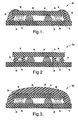
- FIG. 1 is a schematic cross section of an electronic package according to the invention having an overmolding that provides a seal between the perimeter of a surface mount electronic device and a substrate.
- FIG. 2 is a schematic cross section of an electronic package according to the invention having an underfill disposed between surface mount electronic device and a substrate.
- FIG. 3 is a schematic cross section of an electronic package according to the invention having an encapsulant that together with the substrate forms an enclosure around the surface mount electronic device.
- Referring to FIG. 1, an
electronic package 10 comprises asubstrate 12 having printed or otherwise disposed thereon electrically conductive pathways or traces that together with one or more electronic components mounted on the substrate define an electronic component package. A surface mountelectronic device 14 is connected to thecircuit board 12 by asolder joint 16. While the illustrated embodiment includes only a single surface mountelectronic device 14, it should be appreciated thatelectronic package 10 may include any number of surface mountelectronic devices 14 connected tosubstrate 12. -
Substrate 12 may include a printed circuit board having a dielectric substrate and electrically conductive circuitry, such as printed circuit traces as should be evident to those skilled in the art.Substrate 12 may include electrical circuitry fabricated on both the upper and lower surfaces thereof, as well as electrical circuitry located in intermediate layers of the substrate.Substrate 12 may include an organic-based material, such as an organic resin reinforced by fiber, or inorganic material, such as a ceramic substrate or low-temperature, co-fired ceramic LTCC. Examples of circuit board materials include FR4, alumina, metal plated plastic, flex on aluminium, porcelainized steel and other suitable materials. - Formed on an upper surface of
substrate 12 is amounting pad 18, which is electrically connected to the conductive circuitry, and which is used to mechanically and electrically connect aterminal 20 of surface mountelectronic device 14 via asolder joint 16. A solder resist layer (not shown) may be printed on an upper surface of each of themounting pads 18 to define a solder window boundary that contains a volume of reflowed solder. Alternatively, the pads could be laser defined. During a solder reflow process, a reflowed solder ball is reshaped on an upper surface of acorresponding mounting pad 18. - Surface mount
electronic device 14 is mechanically connected and electrically coupled tosubstrate 12. In the illustrated embodiment, surface mountelectronic device 14 includes a plurality ofsolder ball joints 16 attached on a bottom surface near a perimeter ofsurface mount device 14.Solder ball joints 16 may be preformed spherical balls attached tocontact terminals 20 of surface mountelectronic device 14.Solder ball joints 16 may be attached to contactterminals 20 as a solder paste prior to connection onsubstrate 12 or could be applied by solder jet. During assembly, eachsolder joint 16 is aligned and is brought into contact with an electricallyconductive mounting pad 18 on the top surface ofsubstrate 12. In the illustrated embodiment, surface mountelectronic device 14 is a chip, such as a flip chip, having an array ofsolder balls 16 mechanically and electrically coupled tocontact terminals 20 on the bottom side of surface mountelectronic device 14. - Surface mount
electronic device 14 can be any of a number of different types of electronic devices including semiconductor chips, such as flip chips, ball grid arrays, chip-scale packages, and other electronic devices, such as diodes, inductors, capacitors, resistors, varisters, as well as other electrical connecting devices that are mechanically mountable on a surface ofsubstrate 12. - In the illustrated embodiment, surface mount electronic device is a lead-less chip
device having terminals 20 for providing mechanical support connections and electrical signal connections to electrical circuitry on surface mountelectronic device 14.Contact terminals 20 may each include a separate layer of electrically conductive material or may include a conductive surface of the electronic component. Each ofcontact terminals 20 are mechanically and electrically coupled tosubstrate 12 bysolder joints 16. -
Electronic package 10 may include an underfill material 24 (FIG. 2) disposed between surface mountelectronic device 14 andsubstrate 12, an overmold material 26 (FIG. 1) which provides a seal betweensubstrate 12 and the perimeter of surface mountelectronic device 14, or an encapsulant material 28 (FIG. 3), which together with the substrate provides a protective enclosure for surface mountelectronic device 14.Underfill material 24 serves to stabilizesurface mount device 14 by at least partially filling the space betweensurface mount device 14 andsubstrate 12.Underfill material 24 may also serve to adhere surface mountelectronic device 14 tosubstrate 12 and/or serve as a solder flux to enhance wetting of the solder.Underfill 24, overmold 26 andencapsulant 28 also serve to protect surface mount electronic component from damage, such as during handling. -
Underfill material 24 may include a no-flow underfill such as Hysol FF2200, an adhesive such as Chipbonder 3621, a solder flux such as no-clean RMA flux, etc. Eitherunderfill 24, overmold 26, or encapsulant 28 may fill the entire volume between a surface mountelectronic device 14 andsubstrate 12, or only a portion of the volume between surface mountelectronic device 14 andsubstrate 12.Underfill material 24,overmolding material 26 andencapsulating material 28 may also generally comprise a variety of different polymeric materials, such as epoxy resin materials or thermoplastic materials, such as polycarbonate. -
Electronic package 10 includes a plurality ofpolymeric standoffs 30. The term "polymeric" is meant to encompass thermoplastic polymers, thermoset polymers, as well as composite materials having a thermoplastic or thermoset matrix, such as polymer materials containing a property modifying filler. In accordance with the preferred aspects of this invention,polymeric standoffs 30 are precisely positioned in a predetermined pattern using a high precision printing or deposition technique. A preferred technique utilizes microjet printing of a polymeric material, such as an epoxy resin, to form precisely defined structures on the underside of a surface mountelectronic device 14 and/or on the upper surface of asubstrate 12, which definepolymeric standoffs 30. Polymer microjet printing techniques are based on inkjet printing processes which utilize a print head that accurately dispenses picoliter volumes of polymeric formulations at high operating temperatures up to 300°C. Suitable techniques and equipment that may be utilized for precisely formingpolymeric standoffs 30 in accordance with this invention are known in the art and described in the literature. See for example "Microjet Printing of Solder and Polymers for Multi-Chip Modules and Chip-Scale Packages," by Donald J. Hayes, David B. Wallace and W. Royall Cox, MicroFab Technologies, Inc., IMAPS 1999. -
Standoffs 30 in the illustrated embodiments are deposited onsubstrate 12. However, as an equivalent alternative,standoffs 30 may be deposited ondevice 14, or on bothdevice 14 andsubstrate 12. - In addition to thermosets, a low-viscosity, cyclic thermoplastic precursor could be employed, such as those that are available from Cyclics.
- Use of
polymeric standoffs 30 in accordance with the principles of this invention provide structural support for surface mountelectronic devices 14 mounted onsubstrate 12 and prevent or reduce excessive strain or collapse ofdevice 14 during solder reflow and/or during overmolding, underfilling or encapsulation. Unlike no-flow and form-in-place pedestals, additional surface mount technology steps are not required when usingpolymeric standoffs 30 in accordance with this invention. Further, because of the small size and precisely defined structure ofpolymeric standoffs 30, UV curing or solidification of the polymeric standoffs by heating after deposition onsubstrate 12 and/orelectronic device 14 occurs rapidly, and should not adversely affect production time. - During assembly, surface mount
electronic device 14 is brought into contact withsubstrate 12, such thatsolder balls 16contact mounting pads 18. Oncesolder balls 16 have been properly registered with mountingpads 18, solder joints 16 are formed. The solder joints may be formed by applying an elevated temperature (heat) to theelectronic package 10 to cause the solder bumps to reflow on mountingpads 18. During the reflow process, thepolymeric standoffs 30 maintain a separation distance betweensurface mount device 14 andsubstrate 12. Theheated solder balls 16 are reflowed and change shape and are subsequently cooled to solidify and form an electrical and mechanical connection betweenterminals 20 and mountingpads 14. - It should be appreciated that, in addition to preventing collapse of surface mount
electronic device 14 during overmolding or encapsulation,polymeric standoffs 30 achieve a controlled height elevated standoff separation distance betweensurface mount device 14 andsubstrate 12. The controlled standoff height may result in a narrow width solder joint 16, which advantageously provides enhanced vibration properties, while preventing short circuiting with adjacent solder joints 16. - Solder joints 16 may be formed of any of a number of known solder materials. According to one exemplary embodiment, solder joints 16 may be comprised of a tin-lead eutectic solder or a tin-lead-copper solder having a reflow temperature of about 220°C or a Pb-free alloy (reflow temperature approximately 240 to 260°C).
-
Electronic package 10 may be completed by overmolding, encapsulating and/or underfilling operations, which are well-known in the art. Suitable underfilling techniques include underfilling by capillary action between the surface mount electronic device and the substrate, underfilling by compression flow, or "noflow" underfilling. - It will be understood by those who practice the invention and those skilled in the art, that various modifications and improvements may be made to the invention without departing from the spirit of the disclosed concept. The scope of protection afforded is to be determined by the claims and by the breadth of interpretation allowed by law.
Claims (16)
- An electronic package comprising:a substrate having electrically conductive pathways and at least one conductive mounting pad;a surface mount electronic device having at least one terminal;a plurality of polymeric standoffs on at least one of an underside of the surface mount electronic device or an upper surface of the substrate, the standoffs maintaining a desired gap between the underside of the surface mount electronic device and the upper surface of the substrate; andat least one solder joint connecting the terminal of the surface mount device to the mounting pad of the substrate.
- The electronic package of claim 1, further comprising a polymer overmolding that forms a seal between a perimeter of the surface mount electronic device and the substrate.
- The electronic package of claim 1, further comprising a polymer encapsulant that together with the substrate form an enclosure around the surface mount electronic device.
- The electronic package of claim 1, further comprising a polymer underfill disposed between the underside of the surface mount electronic device and the upper surface of the substrate.
- The electronic package of claim 1, wherein the polymeric standoffs are comprised of a thermoset resin.
- The electronic package of claim 1, wherein the polymeric standoffs are comprised of an epoxy resin.
- The electronic package of claim 1, wherein the polymeric standoffs are comprised of a thermoplastic resin.
- A process for making an electronic package comprising:providing a substrate having electrically conductive pathways and at least one conductive mounting pad;providing a surface mount electronic device having at least one terminal;depositing at a plurality of discrete locations on at least one of an underside of the surface mount electronic device or an upper surface of the substrate a solidifiable polymeric material;allowing the deposited material to solidify to form a plurality of polymeric standoffs adhered to at least one of the underside of the surface mount electronic device or the upper surface of the substrate;arranging the terminal of the surface mount electronic device in registry with the mounting pad of the substrate, with a solder ball disposed between the terminal and the mounting pad; andforming a solder joint to electrically and mechanically connect the terminal of the surface mount electronic device to the mounting pad on the substrate.
- The process of claim 8, further comprising overmolding the surface mount electronic device to form a seal between a perimeter of the surface mount electronic device and the substrate.
- The process of claim 8, further comprising encapsulating the surface mount electronic device to enclose the device between an encapsulating material and the substrate.
- The process of claim 8, further comprising underfilling a polymeric material by capillary action between the surface mount electronic device and the substrate.
- The process of claim 8, further comprising underfilling a polymeric material by compression flow or "noflow" underfill between the surface mount electronic device and the substrate.
- The process of claim 8, wherein the polymeric standoffs are comprised of a thermoset resin.
- The process of claim 8, wherein the polymeric standoffs are comprised of an epoxy resin.
- The process of claim 8, wherein the plurality of polymeric standoffs are formed by high temperature microjet printing.
- The process of claim 8, wherein the polymeric standoffs are comprised of a thermoplastic resin.
Applications Claiming Priority (1)
| Application Number | Priority Date | Filing Date | Title |
|---|---|---|---|
| US11/392,019 US20070235217A1 (en) | 2006-03-29 | 2006-03-29 | Devices with microjetted polymer standoffs |
Publications (1)
| Publication Number | Publication Date |
|---|---|
| EP1840952A1 true EP1840952A1 (en) | 2007-10-03 |
Family
ID=38283064
Family Applications (1)
| Application Number | Title | Priority Date | Filing Date |
|---|---|---|---|
| EP07075207A Withdrawn EP1840952A1 (en) | 2006-03-29 | 2007-03-19 | Devices with microjetted polymer standoffs |
Country Status (2)
| Country | Link |
|---|---|
| US (1) | US20070235217A1 (en) |
| EP (1) | EP1840952A1 (en) |
Cited By (2)
| Publication number | Priority date | Publication date | Assignee | Title |
|---|---|---|---|---|
| EP2235747A4 (en) * | 2007-12-26 | 2013-07-03 | Skyworks Solutions Inc | INTEGRATED CIRCUIT CAPACITY WITH IN-SITU-RESONATOR |
| EP4125120A3 (en) * | 2021-07-09 | 2023-06-07 | InnoLux Corporation | Electronic apparatus with an electronic component disposed on and electrically connected to a substrate with at least one spacer interposed therebetween |
Families Citing this family (35)
| Publication number | Priority date | Publication date | Assignee | Title |
|---|---|---|---|---|
| US8310060B1 (en) | 2006-04-28 | 2012-11-13 | Utac Thai Limited | Lead frame land grid array |
| US8461694B1 (en) | 2006-04-28 | 2013-06-11 | Utac Thai Limited | Lead frame ball grid array with traces under die having interlocking features |
| US8492906B2 (en) | 2006-04-28 | 2013-07-23 | Utac Thai Limited | Lead frame ball grid array with traces under die |
| US8460970B1 (en) | 2006-04-28 | 2013-06-11 | Utac Thai Limited | Lead frame ball grid array with traces under die having interlocking features |
| US8487451B2 (en) | 2006-04-28 | 2013-07-16 | Utac Thai Limited | Lead frame land grid array with routing connector trace under unit |
| US7687892B2 (en) * | 2006-08-08 | 2010-03-30 | Stats Chippac, Ltd. | Quad flat package |
| US8125077B2 (en) | 2006-09-26 | 2012-02-28 | Utac Thai Limited | Package with heat transfer |
| US8013437B1 (en) | 2006-09-26 | 2011-09-06 | Utac Thai Limited | Package with heat transfer |
| US9761435B1 (en) | 2006-12-14 | 2017-09-12 | Utac Thai Limited | Flip chip cavity package |
| US9082607B1 (en) | 2006-12-14 | 2015-07-14 | Utac Thai Limited | Molded leadframe substrate semiconductor package |
| US7790512B1 (en) | 2007-11-06 | 2010-09-07 | Utac Thai Limited | Molded leadframe substrate semiconductor package |
| US8063470B1 (en) | 2008-05-22 | 2011-11-22 | Utac Thai Limited | Method and apparatus for no lead semiconductor package |
| US9947605B2 (en) | 2008-09-04 | 2018-04-17 | UTAC Headquarters Pte. Ltd. | Flip chip cavity package |
| JP2010166025A (en) * | 2008-12-19 | 2010-07-29 | Panasonic Corp | Mounting structure |
| US8569877B2 (en) | 2009-03-12 | 2013-10-29 | Utac Thai Limited | Metallic solderability preservation coating on metal part of semiconductor package to prevent oxide |
| US9449900B2 (en) | 2009-07-23 | 2016-09-20 | UTAC Headquarters Pte. Ltd. | Leadframe feature to minimize flip-chip semiconductor die collapse during flip-chip reflow |
| US8368189B2 (en) | 2009-12-04 | 2013-02-05 | Utac Thai Limited | Auxiliary leadframe member for stabilizing the bond wire process |
| US9355940B1 (en) | 2009-12-04 | 2016-05-31 | Utac Thai Limited | Auxiliary leadframe member for stabilizing the bond wire process |
| US8575732B2 (en) | 2010-03-11 | 2013-11-05 | Utac Thai Limited | Leadframe based multi terminal IC package |
| US8871571B2 (en) | 2010-04-02 | 2014-10-28 | Utac Thai Limited | Apparatus for and methods of attaching heat slugs to package tops |
| DE102011000866A1 (en) | 2011-02-22 | 2012-08-23 | Friedrich-Alexander-Universität Erlangen-Nürnberg | Electrical component with an electrical connection arrangement and method for its production |
| US9646942B2 (en) | 2012-02-23 | 2017-05-09 | Taiwan Semiconductor Manufacturing Company, Ltd. | Mechanisms for controlling bump height variation |
| US9449905B2 (en) | 2012-05-10 | 2016-09-20 | Utac Thai Limited | Plated terminals with routing interconnections semiconductor device |
| US9029198B2 (en) | 2012-05-10 | 2015-05-12 | Utac Thai Limited | Methods of manufacturing semiconductor devices including terminals with internal routing interconnections |
| US9006034B1 (en) | 2012-06-11 | 2015-04-14 | Utac Thai Limited | Post-mold for semiconductor package having exposed traces |
| US9679868B2 (en) | 2013-06-19 | 2017-06-13 | Taiwan Semiconductor Manufacturing Company, Ltd. | Ball height control in bonding process |
| MY171261A (en) | 2014-02-19 | 2019-10-07 | Carsem M Sdn Bhd | Stacked electronic packages |
| US10242934B1 (en) | 2014-05-07 | 2019-03-26 | Utac Headquarters Pte Ltd. | Semiconductor package with full plating on contact side surfaces and methods thereof |
| US10269686B1 (en) | 2015-05-27 | 2019-04-23 | UTAC Headquarters PTE, LTD. | Method of improving adhesion between molding compounds and an apparatus thereof |
| US9922843B1 (en) | 2015-11-10 | 2018-03-20 | UTAC Headquarters Pte. Ltd. | Semiconductor package with multiple molding routing layers and a method of manufacturing the same |
| US10276477B1 (en) | 2016-05-20 | 2019-04-30 | UTAC Headquarters Pte. Ltd. | Semiconductor package with multiple stacked leadframes and a method of manufacturing the same |
| CN113972308B (en) * | 2020-07-24 | 2025-08-26 | 群创光电股份有限公司 | Electronic substrate and electronic device |
| US11830833B2 (en) | 2020-07-24 | 2023-11-28 | Innolux Corporation | Electronic substrate and electronic device |
| CN115604938A (en) * | 2021-07-09 | 2023-01-13 | 群创光电股份有限公司(Tw) | Electronic device with a detachable cover |
| CN115706100A (en) * | 2021-08-05 | 2023-02-17 | 群创光电股份有限公司 | Electronic device |
Citations (3)
| Publication number | Priority date | Publication date | Assignee | Title |
|---|---|---|---|---|
| US20020043721A1 (en) * | 1997-10-29 | 2002-04-18 | Weber Patrick O. | Chip package with molded underfill |
| WO2002080261A1 (en) * | 2001-03-28 | 2002-10-10 | International Rectifier Corporation | Wafer level insulation underfill for die attach |
| EP1283548A1 (en) * | 2000-12-21 | 2003-02-12 | Sony Corporation | Sealing resin for flip-flop mounting |
Family Cites Families (17)
| Publication number | Priority date | Publication date | Assignee | Title |
|---|---|---|---|---|
| US4641222A (en) * | 1984-05-29 | 1987-02-03 | Motorola, Inc. | Mounting system for stress relief in surface mounted components |
| US4731130A (en) * | 1987-05-27 | 1988-03-15 | Gte Government Systems Corporation | Soldering composition |
| US5315070A (en) * | 1991-12-02 | 1994-05-24 | Siemens Aktiengesellschaft | Printed wiring board to which solder has been applied |
| US5328521A (en) * | 1993-03-08 | 1994-07-12 | E. I. Du Pont De Nemours And Company | Kinetic solder paste composition |
| US5700715A (en) * | 1994-06-14 | 1997-12-23 | Lsi Logic Corporation | Process for mounting a semiconductor device to a circuit substrate |
| EP0854768A1 (en) * | 1995-10-06 | 1998-07-29 | Brown University Research Foundation | Soldering methods and compositions |
| US5977629A (en) * | 1996-01-24 | 1999-11-02 | Micron Technology, Inc. | Condensed memory matrix |
| US5681757A (en) * | 1996-04-29 | 1997-10-28 | Microfab Technologies, Inc. | Process for dispensing semiconductor die-bond adhesive using a printhead having a microjet array and the product produced by the process |
| US5931371A (en) * | 1997-01-16 | 1999-08-03 | Ford Motor Company | Standoff controlled interconnection |
| US5891753A (en) * | 1997-01-24 | 1999-04-06 | Micron Technology, Inc. | Method and apparatus for packaging flip chip bare die on printed circuit boards |
| US5926731A (en) * | 1997-07-02 | 1999-07-20 | Delco Electronics Corp. | Method for controlling solder bump shape and stand-off height |
| DE69809787T2 (en) * | 1997-10-02 | 2003-09-18 | Matsushita Electric Industrial Co., Ltd. | ASSEMBLY METHOD FOR SEMICONDUCTOR COMPONENTS ON A PCB |
| US6046910A (en) * | 1998-03-18 | 2000-04-04 | Motorola, Inc. | Microelectronic assembly having slidable contacts and method for manufacturing the assembly |
| US6631078B2 (en) * | 2002-01-10 | 2003-10-07 | International Business Machines Corporation | Electronic package with thermally conductive standoff |
| US6986454B2 (en) * | 2003-07-10 | 2006-01-17 | Delphi Technologies, Inc. | Electronic package having controlled height stand-off solder joint |
| US7390874B2 (en) * | 2003-12-29 | 2008-06-24 | Kuboyama Bio Ken, Inc. | Peptide, method of production thereof, and pharmaceutical composition containing the same |
| US7202571B2 (en) * | 2004-08-16 | 2007-04-10 | Delphi Technologies, Inc. | Electronic module with form in-place pedestal |
-
2006
- 2006-03-29 US US11/392,019 patent/US20070235217A1/en not_active Abandoned
-
2007
- 2007-03-19 EP EP07075207A patent/EP1840952A1/en not_active Withdrawn
Patent Citations (3)
| Publication number | Priority date | Publication date | Assignee | Title |
|---|---|---|---|---|
| US20020043721A1 (en) * | 1997-10-29 | 2002-04-18 | Weber Patrick O. | Chip package with molded underfill |
| EP1283548A1 (en) * | 2000-12-21 | 2003-02-12 | Sony Corporation | Sealing resin for flip-flop mounting |
| WO2002080261A1 (en) * | 2001-03-28 | 2002-10-10 | International Rectifier Corporation | Wafer level insulation underfill for die attach |
Non-Patent Citations (1)
| Title |
|---|
| D. J. HAYES, D. B. WALLACE, W.R. COX: "MicroJet Printing of Solder and Polymers for Multi-Chip Modules and Chip-Scale Packages", 1999 INTERNATIONAL CONFERENCE ON HIGH DENSITY PACKAGING AND MCMS, 1999, pages 242 - 247, XP009087488 * |
Cited By (4)
| Publication number | Priority date | Publication date | Assignee | Title |
|---|---|---|---|---|
| EP2235747A4 (en) * | 2007-12-26 | 2013-07-03 | Skyworks Solutions Inc | INTEGRATED CIRCUIT CAPACITY WITH IN-SITU-RESONATOR |
| US8900931B2 (en) | 2007-12-26 | 2014-12-02 | Skyworks Solutions, Inc. | In-situ cavity integrated circuit package |
| US9153551B2 (en) | 2007-12-26 | 2015-10-06 | Skyworks Solutions, Inc. | Integrated circuit package including in-situ formed cavity |
| EP4125120A3 (en) * | 2021-07-09 | 2023-06-07 | InnoLux Corporation | Electronic apparatus with an electronic component disposed on and electrically connected to a substrate with at least one spacer interposed therebetween |
Also Published As
| Publication number | Publication date |
|---|---|
| US20070235217A1 (en) | 2007-10-11 |
Similar Documents
| Publication | Publication Date | Title |
|---|---|---|
| US20070235217A1 (en) | Devices with microjetted polymer standoffs | |
| US6338985B1 (en) | Making chip size semiconductor packages | |
| US12278205B2 (en) | Semiconductor device package with improved die pad and solder mask design | |
| US8445322B2 (en) | Method of fabricating semiconductor package | |
| KR101837511B1 (en) | Semiconductor package and method of manufacturing the same | |
| US7807510B2 (en) | Method of manufacturing chip integrated substrate | |
| JP2002252303A (en) | Flip chip semiconductor device in molded chip scale package and assembling method | |
| US20150318228A1 (en) | Module and method for producing module | |
| US20020110956A1 (en) | Chip lead frames | |
| US7118940B1 (en) | Method of fabricating an electronic package having underfill standoff | |
| KR20120050755A (en) | Semiconductor package substrate and method for manufacturing the same | |
| US6657313B1 (en) | Dielectric interposer for chip to substrate soldering | |
| US20090017582A1 (en) | Method for manufacturing semiconductor device | |
| JP2907188B2 (en) | Semiconductor device, method of mounting semiconductor device, and method of manufacturing semiconductor device | |
| KR20070076084A (en) | Stacked package and its manufacturing method | |
| US5961032A (en) | Method of fabrication of a multi-component solder column by blocking a portion of a through hole in a mold | |
| JP4001778B2 (en) | Circuit module and manufacturing method thereof | |
| US20050196907A1 (en) | Underfill system for die-over-die arrangements | |
| KR20050033606A (en) | Negative volume expansion lead-free electrical connection | |
| US20060175702A1 (en) | Ball grid array package | |
| KR101255925B1 (en) | Semiconductor package and method for manufacturing the same | |
| KR100665288B1 (en) | Flip chip package manufacturing method | |
| CN114375494A (en) | Electronic component, method for manufacturing electronic component, mounted structure, and method for manufacturing mounted structure | |
| US12185470B2 (en) | Embedded printed circuit board | |
| JP2001007503A (en) | Electronic component mounting method |
Legal Events
| Date | Code | Title | Description |
|---|---|---|---|
| PUAI | Public reference made under article 153(3) epc to a published international application that has entered the european phase |
Free format text: ORIGINAL CODE: 0009012 |
|
| AK | Designated contracting states |
Kind code of ref document: A1 Designated state(s): AT BE BG CH CY CZ DE DK EE ES FI FR GB GR HU IE IS IT LI LT LU LV MC MT NL PL PT RO SE SI SK TR |
|
| AX | Request for extension of the european patent |
Extension state: AL BA HR MK YU |
|
| 17P | Request for examination filed |
Effective date: 20080403 |
|
| AKX | Designation fees paid |
Designated state(s): AT BE BG CH CY CZ DE DK EE ES FI FR GB GR HU IE IS IT LI LT LU LV MC MT NL PL PT RO SE SI SK TR |
|
| 17Q | First examination report despatched |
Effective date: 20080521 |
|
| STAA | Information on the status of an ep patent application or granted ep patent |
Free format text: STATUS: THE APPLICATION IS DEEMED TO BE WITHDRAWN |
|
| 18D | Application deemed to be withdrawn |
Effective date: 20101001 |