EP1840587A2 - Magnetic detection device having magnetic detection element in magnetic detection circuit and fabricating method thereof - Google Patents
Magnetic detection device having magnetic detection element in magnetic detection circuit and fabricating method thereof Download PDFInfo
- Publication number
- EP1840587A2 EP1840587A2 EP07006575A EP07006575A EP1840587A2 EP 1840587 A2 EP1840587 A2 EP 1840587A2 EP 07006575 A EP07006575 A EP 07006575A EP 07006575 A EP07006575 A EP 07006575A EP 1840587 A2 EP1840587 A2 EP 1840587A2
- Authority
- EP
- European Patent Office
- Prior art keywords
- magnetic detection
- layer
- detection element
- magnetic
- flat surface
- Prior art date
- Legal status (The legal status is an assumption and is not a legal conclusion. Google has not performed a legal analysis and makes no representation as to the accuracy of the status listed.)
- Withdrawn
Links
- 230000005291 magnetic effect Effects 0.000 title claims abstract description 253
- 238000001514 detection method Methods 0.000 title claims abstract description 219
- 238000000034 method Methods 0.000 title claims description 41
- 239000000758 substrate Substances 0.000 claims abstract description 35
- 230000000694 effects Effects 0.000 claims abstract description 23
- 238000004519 manufacturing process Methods 0.000 claims description 7
- 230000000149 penetrating effect Effects 0.000 abstract description 3
- 239000000463 material Substances 0.000 description 9
- VYPSYNLAJGMNEJ-UHFFFAOYSA-N Silicium dioxide Chemical compound O=[Si]=O VYPSYNLAJGMNEJ-UHFFFAOYSA-N 0.000 description 8
- 230000005290 antiferromagnetic effect Effects 0.000 description 7
- 239000010949 copper Substances 0.000 description 7
- 239000010408 film Substances 0.000 description 7
- 230000005415 magnetization Effects 0.000 description 7
- RYGMFSIKBFXOCR-UHFFFAOYSA-N Copper Chemical compound [Cu] RYGMFSIKBFXOCR-UHFFFAOYSA-N 0.000 description 6
- 238000013459 approach Methods 0.000 description 6
- 238000006243 chemical reaction Methods 0.000 description 6
- 229910052802 copper Inorganic materials 0.000 description 6
- 229910045601 alloy Inorganic materials 0.000 description 5
- 239000000956 alloy Substances 0.000 description 5
- 238000007747 plating Methods 0.000 description 5
- 238000004544 sputter deposition Methods 0.000 description 5
- VYZAMTAEIAYCRO-UHFFFAOYSA-N Chromium Chemical compound [Cr] VYZAMTAEIAYCRO-UHFFFAOYSA-N 0.000 description 4
- 229910000914 Mn alloy Inorganic materials 0.000 description 4
- 238000002161 passivation Methods 0.000 description 4
- 239000000377 silicon dioxide Substances 0.000 description 4
- 239000010409 thin film Substances 0.000 description 4
- 229910001030 Iron–nickel alloy Inorganic materials 0.000 description 3
- 229910003271 Ni-Fe Inorganic materials 0.000 description 3
- 230000001413 cellular effect Effects 0.000 description 3
- 238000010586 diagram Methods 0.000 description 3
- PCHJSUWPFVWCPO-UHFFFAOYSA-N gold Chemical compound [Au] PCHJSUWPFVWCPO-UHFFFAOYSA-N 0.000 description 3
- 229910052737 gold Inorganic materials 0.000 description 3
- 239000010931 gold Substances 0.000 description 3
- 238000000059 patterning Methods 0.000 description 3
- 229910052709 silver Inorganic materials 0.000 description 3
- 239000004332 silver Substances 0.000 description 3
- 238000000992 sputter etching Methods 0.000 description 3
- 229910020598 Co Fe Inorganic materials 0.000 description 2
- 229910002519 Co-Fe Inorganic materials 0.000 description 2
- 229910001313 Cobalt-iron alloy Inorganic materials 0.000 description 2
- 229910052581 Si3N4 Inorganic materials 0.000 description 2
- XAGFODPZIPBFFR-UHFFFAOYSA-N aluminium Chemical compound [Al] XAGFODPZIPBFFR-UHFFFAOYSA-N 0.000 description 2
- 229910052782 aluminium Inorganic materials 0.000 description 2
- PNEYBMLMFCGWSK-UHFFFAOYSA-N aluminium oxide Inorganic materials [O-2].[O-2].[O-2].[Al+3].[Al+3] PNEYBMLMFCGWSK-UHFFFAOYSA-N 0.000 description 2
- 230000015572 biosynthetic process Effects 0.000 description 2
- 230000007423 decrease Effects 0.000 description 2
- 238000010030 laminating Methods 0.000 description 2
- 239000000696 magnetic material Substances 0.000 description 2
- 235000012239 silicon dioxide Nutrition 0.000 description 2
- HQVNEWCFYHHQES-UHFFFAOYSA-N silicon nitride Chemical compound N12[Si]34N5[Si]62N3[Si]51N64 HQVNEWCFYHHQES-UHFFFAOYSA-N 0.000 description 2
- XUIMIQQOPSSXEZ-UHFFFAOYSA-N Silicon Chemical compound [Si] XUIMIQQOPSSXEZ-UHFFFAOYSA-N 0.000 description 1
- 229910052593 corundum Inorganic materials 0.000 description 1
- 230000008878 coupling Effects 0.000 description 1
- 238000010168 coupling process Methods 0.000 description 1
- 238000005859 coupling reaction Methods 0.000 description 1
- 230000002708 enhancing effect Effects 0.000 description 1
- 239000011810 insulating material Substances 0.000 description 1
- SHMWNGFNWYELHA-UHFFFAOYSA-N iridium manganese Chemical compound [Mn].[Ir] SHMWNGFNWYELHA-UHFFFAOYSA-N 0.000 description 1
- 239000004973 liquid crystal related substance Substances 0.000 description 1
- IGOJMROYPFZEOR-UHFFFAOYSA-N manganese platinum Chemical compound [Mn].[Pt] IGOJMROYPFZEOR-UHFFFAOYSA-N 0.000 description 1
- 230000001590 oxidative effect Effects 0.000 description 1
- 238000005498 polishing Methods 0.000 description 1
- 239000004065 semiconductor Substances 0.000 description 1
- 229910052710 silicon Inorganic materials 0.000 description 1
- 239000010703 silicon Substances 0.000 description 1
- 229910001845 yogo sapphire Inorganic materials 0.000 description 1
Images


Classifications
-
- G—PHYSICS
- G01—MEASURING; TESTING
- G01R—MEASURING ELECTRIC VARIABLES; MEASURING MAGNETIC VARIABLES
- G01R33/00—Arrangements or instruments for measuring magnetic variables
- G01R33/02—Measuring direction or magnitude of magnetic fields or magnetic flux
- G01R33/06—Measuring direction or magnitude of magnetic fields or magnetic flux using galvano-magnetic devices
- G01R33/09—Magnetoresistive devices
Definitions
- the present invention relates to a magnetic detection device and a fabrication method thereof.
- the magnetic detection device includes a magnetic detection element and a detection circuit that detects an electrical resistance of the magnetic detection element that detects an external magnetic field.
- the magnetic detection device is formed in a small-area package.
- the magnetic detection device works due to magneto-resistance effect, like anisotropic magneto-resistance effect (an AMR effect), a giant magneto-resistance effect (GMR effect) and tunnel magneto-resistance effect (TMR effect).
- AMR effect anisotropic magneto-resistance effect
- GMR effect giant magneto-resistance effect
- TMR effect tunnel magneto-resistance effect
- a magnetic detection device detecting an external magnetic field is used for a non-contact ON-OFF switch, a rotary encoder detecting a phase of rotation or the number of rotations, and the like.
- a known magnetic detection device mainly uses a hall element as a magnetic detection element.
- a magnetic detection device using a hall element has a disadvantage that a circuit configuration of a detection circuit is complex because a correction circuit is necessary for a detection output.
- a magnetic detection element using a magneto-resistance effect has an advantage that the circuit configuration of the detection circuit can be relatively simple and detect the external magnetic field with high precision.
- Patent Document 1 Japanese Unexamined Patent Application Publication No. 8-279326 .
- the present invention is contrived to solve the above-mentioned problems. It is an object of the present invention to provide a magnetic detection device capable of integrating a magnetic detection element and a detection circuit in a small area.
- a magnetic detection device including a magnetic detection element with a multi-layered film structure of which an electric resistance varies with an external magnetic field using a magneto-resistance effect and a detection circuit detecting a variation in electric resistance of the magnetic detection element.
- an active element and an interconnection layer constituting the detection circuit are formed on a substrate, at least a portion on the surface of an insulating layer covering the active element layer and the interconnection layer is planarized into a flat surface, the magnetic detection element is formed on the flat surface, and the interconnection layer on the substrate and the magnetic detection element on the insulating layer are electrically connected to each other.
- the magnetic detection element is disposed on the insulating layer covering the active element constituting a detection circuit, thereby forming an integrated device in a small area.
- a surface of the insulating layer is planarized, so the magnetic detection element of a structure of multi-layered film is formed on the flat surface, thereby easily forming the magnetic detection element. Therefore, a dimensional precision of the magnetic detection element can be achieved with high precision, thereby obtaining the magnetic detection element with high detection precision.
- the magnetic detection element is able to detect an external magnetic field by using a magneto-resistance effect,like anisotropic magneto-resistance effect (an AMR effect), a giant magneto-resistance effect (a GMR effect), or a tunnel magneto-resistance effect (TMR effect).
- a magneto-resistance effect like anisotropic magneto-resistance effect
- a GMR effect giant magneto-resistance effect
- TMR effect tunnel magneto-resistance effect
- a fixed resistance element is formed of the same film as the magnetic detection element and an electric resistance thereof does not vary with the external magnetic field, wherein the fixed resistance element and the magnetic detection element are connected to each other in series and formed on the flat surface, and a connection point between the magnetic detection element and the fixed resistance element is electrically connected to the interconnection layer.
- both the magnetic detection element and the fixed resistance element are formed on the flat surface of the insulating layer, both the magnetic detection element and the fixed resistance element can be formed with high precision.
- the magnetic detection element and the fixed resistance element can be disposed in the same condition, thereby enhancing an output precision of a central voltage of both elements.
- an electrode layer of the magnetic detection element or a lead layer extending from the electrode layer which is formed on the flat surface may be disposed just above the interconnection layer and the electrode layer and the interconnection layer or the lead layer and the interconnection layer which are disposed above and below each other may be electrically connected to each other.
- the device can be formed in a small area rather than expanding the interconnection and lead layers to be two-dimensionally disposed.
- a bridge circuit has the magnetic detection element, wherein a reference resistance element constituting the bridge circuit is formed on the substrate together with the active element.
- the magnetic detection device which includes a magnetic detection element with a multi-layered film structure of which an electric resistance varies with an external magnetic field using a magneto-resistance effect and a detection circuit detecting a variation in electric resistance of the magnetic detection element, and the method has steps as below.
- An active element and an interconnection layer constituting the detection circuit are formed on a substrate, at least a portion of the surface of an insulating layer covering the active element and the interconnection layer is planarized into a flat surface, the magnetic detection element is formed on the flat surface, and the interconnection layer on the substrate and the magnetic detection element electrically connect to each other on the insulating layer.
- the detection circuit is formed on the substrate and covered with an insulating layer. Additionally, a surface of the insulating layer is planarized and then the magnetic detection element is formed on the flat surface. Accordingly, a laminated body laminated sequentially from the substrate to the insulating layer is treated same as the substrate, whereby the magnetic detection element can be formed on the flat surface in terms of a thin film laminating process, thereby excellently producing in large quantities.
- a fixed resistance element which is formed of the same film as the magnetic detection element and of which electric resistance does not vary with the external magnetic field is formed so as to be electrically connected in series to the magnetic detection element on the flat surface, and a connection point between the magnetic detection element and the fixed resistance element can be electrically connected to the interconnection layer.
- an electrode layer of the magnetic detection element is formed on the flat surface, the electrode layer or a lead layer extending from the electrode layer is formed just above the interconnection layer, and the electrode layer and the interconnection layer or the lead layer and the interconnection layer which are disposed above and below each other may be electrically connected to each other.
- the magnetic detection device In the method of fabricating the magnetic detection device according to the invention, it is possible to form a bridge circuit having the magnetic detection element and to form a reference resistance element constituting the bridge circuit on the substrate together with the active element.
- a surface of the insulating layer is planarized after forming the insulating layer of the substrate and the detection circuit. Accordingly, a laminated body of the substrate, the detection circuit, and the insulating layer is treated same as the substrate, whereby the magnetic detection element or the fixed resistance element can be formed on the flat surface in terms of a thin film laminating process, thereby suitably producing in large quantities.
- Fig. 1 is a perspective view illustrating a magnetic detection device according to a first embodiment of the invention.
- Fig. 2 is a longitudinal sectional view illustrating the magnetic detection device shown in Fig. 1 taken along Line II-II.
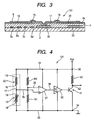
- Fig. 4 is a circuit configuration diagram illustrating the magnetic detection device.
- Fig. 5A is an enlarged sectional view illustrating a film formation of a magnetic detection element.
- Fig. 5B is an enlarged sectional view illustrating a film formation of a fixed resistance element.
- the magnetic detection device 1 shown in Fig. 1 is a unified IC package of a magnetic detection element 10, a fixed resistance element 20, and a detection circuit and is formed small and thinly.
- the magnetic detection device 1 can obtain an ON output of a pulse shape when a magnetic field generating member such as a magnet M approaches.
- the magnetic detection device 1 is built in a core portion on which key switches are arranged in a foldable cellular phone.
- the magnet M is mounted on a foldable portion having a display device such as a liquid crystal device. When the core portion and the foldable portion are folded to contact with each other, the magnet M approaches the magnetic detection device 1, and then the magnetic detection device 1 detects an external magnetic field generated by the magnet M, thereby obtaining the ON output from the magnetic detection device 1.
- An arrangement position of the magnetic detection device 1 is not limited to the foldable cellular phone and may be mounted on, for example, a car to be used in a position detecting portion of a sheet, a detachment detecting portion of a safety belt, or the like. Alternatively, it is possible to be used for checking the phase of a rotation or the number of rotations of a magnet by changing a circuit configuration.
- the device is constituted as shown in Fig. 4 so as to obtain the ON output by detecting the magnetic field generated from the magnet M or the like.
- a magnetic detection element 10 and a fixed resistance element 20 are mounted on the magnetic detection device 1.
- An electric resistance of the magnetic detection element 10 varies by using a magneto-resistance effect.
- the fixed resistance element 20 has basically the same electric resistance and temperature characteristic as the magnetic detection element 10. Additionally, the electric resistance practically does not vary with the magnitude of an external magnetic field to which the magnetic detection element 10 reacts.
- the magnetic detection element 10 detects the external magnetic field by using a giant magneto-resistance effect (a GMR effect). As shown in Fig. 5A, from the lower surface of the magnetic detection element 10, it is sequentially laminated in order of an antiferromagnetic layer 11 formed of an Ir-Mn alloy (an iridium-manganese alloy), a Pt-Mn alloy (a platinum-manganese alloy), or the like, and a fixed magnetic layer 12 formed of a soft magnetic material such as a Co-Fe alloy (a cobalt-iron alloy) or a Ni-Fe alloy (a nickel-iron alloy).
- a GMR effect giant magneto-resistance effect
- a non-magnetic intermediate layer 13 formed of such as Cu (a copper) and the Ni-Fe alloy (the nickel-iron alloy)
- a detection magnetic layer (a free magnetic layer) 14 formed of the soft magnetic material such as the Co-Fe alloy (the cobalt-iron alloy) or the Ni-Fe alloy (the nickel-iron alloy).
- a shape of a plane of the magnetic detection element 10 is formed in a meander pattern, so its basic electric resistance increases.
- a magnetization direction of the fixed magnetic layer 12 is fixed perpendicular to a Pin direction shown in Fig. 1, that is, a length direction of the magnetic detection element 10. Accordingly, as shown in Fig. 1, when an N pole of the magnet M approaches, a magnetization direction of a detection magnetic layer 14 becomes opposite to the Pin direction and an electric resistance of the magnetic detection element 10 is maximized.
- the magnet M withdraws farther and an external magnetization acting on the detecting magnetic layer 14 disappears the resistance of the magnetic detection element 10 is minimized.
- Fig. 5B it is sequentially laminated from the lower surface of the fixed resistance element 20 in order of the antiferromagnetic layer 11 and a fixed magnetic layer 12.
- the magnetization direction of the fixed magnetic layer 12 is fixed to a Pin direction same as the fixed magnetic layer 12 of the magnetic detection element 10.
- it is sequentially laminated in order of the detection magnetic layer 14 and the non-magnetic intermediate layer 13 on the fixed magnetic layer 12.
- a laminated order of the detection magnetic layer 14 and the non-magnetic intermediate layer 13 is opposite to the magnetic detection element 10.
- the electric resistance practically does not vary even when the external magnetic field to which the magnetic detection element 10 reacts, that is, the external magnetic field having the magnitude which varies the resistance of the magnetic detection element 10 acts.
- the fixed resistance element 20 constituted of the antiferromagnetic layer 11, the fixed magnetic layer 12, the detection magnetic layer 14, the non-magnetic intermediate layer 13 has the same material and thickness as each layer constituting the magnetic detection element 10. Additionally, as shown in Fig. 1, the fixed resistance element 20 is two-dimensionally formed in the meander pattern same as the magnetic detection element 10. Therefore, the fixed resistance element 20 has the same electric resistance as the magnetic detection element 10 and its temperature characteristic is same as well. In addition, the magnetic detection element 10 and the fixed resistance element 20 are disposed on the same surface, whereby both elements 10 and 20 are disposed in the same temperature condition.
- each resistance can be increased high, thereby reducing a current consumption.
- the external magnetic field acts, it is possible to obtain an adequate central potential.
- an electrode layer 15 formed of a low-resistance material is formed in one end of the magnetic detection element 10 and an electrode layer 18 formed of the low-resistance material is similarly formed in the other end thereof.
- An electrode layer 16 formed of the low-resistance material is formed in one end of the fixed resistance element 20 and an electrode layer 19 formed of the low-resistance material is similarly formed in the other end thereof.
- the electrode layer 15 of the magnetic detection element 10 and the electrode layer 16 of the fixed resistance element 20 are connected to a lead layer 17, and the magnetic detection element 10 and the fixed resistance element 20 are connected to each other in series.
- the electrode and lead layers are mainly formed of a low-resistance material such as a gold, a silver, a copper, and the like, for example, it is sequentially laminated in order of a chrome, a copper, and a chrome.
- reference resistance elements R1 and R2 are connected to each other in series.
- a bridge circuit is formed by connecting a series group of the magnetic detection element 10 and the fixed resistance element 20 to a series group of the reference resistance elements R1 and R2 in parallel. Then, as shown in Fig. 1, one end of both series groups of the bridge circuit is connected to a electrical power supply pad 32 exposed on the magnetic detection device 1 via a electrical power supply interconnection layer 31. The other end of both series groups is connected to a ground pad 34 exposed on the magnetic detection device 1 via a ground interconnection layer 33.
- the ground pad 34 is set to a ground potential.
- the lead layer 17 connecting the magnetic detection element 10 to the fixed resistance element 20 in series is connected to a central interconnection layer 35, and the central interconnection layer 35 is connected to a + input portion of a differential amplifier 37.
- a connection point of the reference resistances R1 and R2 is connected to a central interconnection layer 36 and the central interconnection layer 36 is connected to a - input portion of the differential amplifier 37.
- the detection circuit is formed of a circuit element other than the magnetic detection element 10 of the circuit configuration shown in Fig. 4.
- a plurality of the magnetic detection devices 1 are formed on a substrate 2 made of a silicon (Si) and then each magnetic detection device 1 is divided together with the substrate 2 by a dicing process.
- Si silicon
- An underlying layer made of a silicon dioxide (SiO 2 ) is formed on the substrate 2 with a predetermined thickness (not shown).
- the active element and the interconnection layer constituting the differential amplifier 37, the active element layer and the interconnection layer constituting the comparator 39, the active element constituting the output transistor 41, and the like are formed on the underlying layer by a thin film process.
- a forming of the active element layer and the interconnection layer is performed by such as a CVD process, a sputtering process, and a plating process.
- each active element together with the reference resistance elements R1 and R2 and the output resistance 43 are formed on a surface of the underlying layer.
- Each active element, resistance elements, and the like are two-dimensionally arranged on the surface of the underlying layer and are formed. Additionally, a portion of the active elements or the resistance elements may be laminated and is formed. As shown in Fig. 2, the active elements or the resistance elements are indicated as circuit elements 3a, 3b, 3c, and 3d.
- the interconnection layers 31, 33, 35, 36, and 38 are formed on the surface of the underlying layer by the sputtering or plating processes, respectively.
- the interconnection layers 31, 33, 35, 36, and 38 are formed of the low-resistance material, for example, an aluminum.
- the interconnection layers 31, 33, 35, 36, and 38 of the magnetic detection device 1 formed with a width of 1.0 ⁇ m or more and a thickness of 3 ⁇ m or less.
- an insulating layer 4 which is a passivation layer is formed above thereof.
- the insulating layer 4 is formed by a CVD process or the sputtering process.
- a surface of the insulating layer 4 is polished to be a flat surface 4a by a CMP method.
- the insulating layer 4 is made of, for example, a silicon nitride (Si 3 N 4 ) and the like.
- the flat surface 4a may be partially formed on an area disposing the magnetic detection element 10 and the fixed resistance element 20, the flat surface 4a is formed on a total area of the surface of the insulating layer 4 in the embodiment.
- Plural sets of the circuit elements 3a, 3b, 3c, and 3d and the interconnection layers 31, 33, 35, 36, and 38 to form a plurality of the magnetic detection devices 1 are formed on the large substrate 2, and then all of them are covered with the insulating layer 4.
- a plurality of the flat surfaces 4a of the magnetic detection device 1 are able to be formed at the same time by forming the flat surface 4a in terms of polishing the total area of the surface by a CMP method and the like.
- the laminated body thereof can be treated as one substrate. So, even when the laminated body is exposed to the atmosphere, it is possible to prevent the laminated body from oxidizing because the circuit elements 3a, 3b, 3c, and 3d and the interconnection layers 31, 33, 35, 36, and 38 are covered with the insulating layer 4.
- the magnetic detecting element 10 of the laminated body shown in Fig. 5A is formed on the flat surface 4a, that is, a surface of the laminated body by the CVD process, the sputtering process, or the plating process. In this process, it is subsequently laminated in order of the antiferromagnetic layer 11, the fixed magnetic layer 12, the non-magnetic intermediate layer 13, and the detection magnetic layer 14 on a total surface of the flat surface 4a. Then, a resist layer is formed on the surface thereof.
- each layer of a portion which is not covered with the resist layer is removed by an ion-milling process, whereby the magnetic detection element 10 of a meander pattern is formed on the flat surface 4a as shown in Fig. 1.
- the magnetic detection element 10 is covered with the resist layer. In the other portion, it is laminated from the bottom of the total surface of the flat surface 4a in order of the antiferromagnetic layer 11, the fixed magnetic layer 12, the detection magnetic layer 14, and the non-magnetic intermediate layer 13 as shown in Fig. 5B.
- the thickness of each of theses layers 11, 12, 14, and 13 is set to be equal to that of each of layers 11, 12, 13, and 14 of the magnetic detection element 10.
- the resist layer is formed on thereof.
- the patterning is performed on the resist layer, and then each layer of the portion which is not covered with the resist layer is removed by the ion-milling process, so that the fixed resistance element 20 of the meander pattern can be formed as shown in Fig. 1. Furthermore, the resist layer covering the magnetic detection element 10 and the fixed resistance element 20 is removed by a lift-off process.
- the magnetization direction of the fixed magnetic layer 12 of the magnetic detection element 10 is fixed to the Pin direction.
- the magnetization direction of the fixed magnetic layer 12 of the fixed resistance element 20 is together fixed.
- the electric resistance of the fixed resistance element 20 does not vary practically since it is sequentially laminated in order of the fixed magnetic layer 12, the detection magnetic layer 14, and the non-magnetic intermediate layer 13.
- the resist layer is formed on the surface of the flat surface 4a, and the patterning is performed on the resist layer.
- the electrode layers 15, 16, 18, and 19, the lead layer 17, and the pads 32, 34, and 42 mainly formed of the low-resistance material are formed by the plating process on a portion in which the resist layer is removed.
- Each of these layers is mainly formed of the low-resistance material such as the gold, the silver, and the copper, and, for example, the laminated body sequentially laminated in order of the chrome, the copper, and the chrome.
- the lead layer 17 connecting the magnetic detection element 10 to the fixed resistance element 20 in series is formed above the central interconnection layer 35 shown in Fig. 4. Additionally, as shown in Fig. 2, a bump 5 penetrating the insulating layer 4 is formed on the central interconnection layer 35 before forming the lead layer 17 on the flat surface 4a. The lead layer 17 and the central interconnection layer 35 are electrically connected to each other via the bump 5.
- the bump 5 is formed of such as the gold, the silver, the copper, and the aluminum.
- an electrode layer 18 formed on an end of the magnetic detection element 10 is formed just above the electrical power supply interconnection layer 31 formed on the surface of the substrate 2.
- the electrode layer 18 and the electrical power supply interconnection layer disposed above and below thereof are connected to each other via the bump.
- An electrode layer 19 formed on an end of the fixed resistance element 20 is formed just above the ground interconnection layer 33 formed on the substrate 2.
- the electrode and ground interconnection layers 19 and 33 disposed above and below thereof are connected to each other via the bump.
- the electrical power supply interconnection layer 31 is disposed below the electrical power supply pad 32
- the ground interconnection layer 33 is disposed below the ground pad 34
- the interconnection layer is disposed below the output pad 42.
- the electrical power supply pad 32, the ground pad 34, and the output pad 42 are connected to the interconnection layer disposed below thereof via the bump.
- the interconnection layer is formed below the electrode layers 15, 16, 18, and 19, the lead layer 17, and each of the pads 32, 34, and 42 on the substrate 2, so that the electrode layer and the interconnection layer, the lead layer and the interconnection layer, and the pad and the interconnection layer are electrically connected via the bump penetrating the upper and lower sides of the insulating layer 4, respectively. Consequently, it is possible to form the magnetic detection device 1 in a small area.
- the magnetic detection element 10, the fixed resistance element 20, the electrode layers 15, 16, 18, and 19, and the lead layer 17 are covered with the passivation layer 6.
- the passivation layer 6 is formed of an insulating material such as an alumina (Al 2 O 3 ) and a silicon dioxide (SiO 2 ) by the sputtering process.
- the electrical power supply pad 32, the ground pad 34, and the output pad 42 shown in Fig. 1 are not covered with the passivation layer 6, and theses pads are exposed.
- the substrate 2 is divided by a dicing process, so that each individual magnetic detection device 1 shown in Fig. 1 is obtained.
- the circuit elements 3a, 3b, 3c, and 3d and each of the interconnection layers 31, 33, 35, 36, and 38 are formed on the substrate 2, and then the insulating layer 4 is formed on thereof. Since the total area of the surface of the insulating layer 4 is the flat surface 4a, this laminated body is treated as the substrate, so that the magnetic detection element 10, the fixed resistance element 20, the electrode layers 15, 16, 18, and 19, the lead layer 17, and each of the pads 32, 34, and 42 can be formed on the flat surface 4a by the thin film process.
- Fig. 3 is a longitudinal sectional view illustrating a magnetic detection device 101 according to a second embodiment of the invention.
- the same portions of configuration elements of the magnetic detection device 101 as the magnetic detection device 1 according to the first embodiment will be marked with the same numeral as the magnetic detection device 1, and the description of the same portions will be omitted.
- the bump 5 is not formed, and a lead layer 17 and a central interconnection layer 35 disposed below the lead layer 17 are directly connected to each other.
- the insulating layer 4 is punched by an ion-milling process before and after a flat surface 4a is formed, and then a lead layer 17 is formed by the plating and the like, thereby directly connecting the lead layer 17 to the central interconnection layer 35.
- the connection of other electrode layers 18 and 19 to the interconnection layer, and each of pads 32, 34, and 42 to the interconnection layer are performed in the same way as above.
- the connection method using the bump 5 and the above-mentioned direct connection method can be used together.
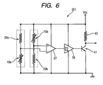
- a circuit configuration of a magnetic detection device 201 according to a third embodiment is described in Fig. 6.
- a pair of magnetic detection elements 10a and 10b having the same laminated structure as shown in Fig. 5A, and a pair of fixed resistance elements 20a and 20b having the same laminated structure as shown in Fig. 5B are used.
- the magnetic detection elements 10a and 10b and the fixed resistance elements 20a and 20b are formed on a flat surface 4a of an insulating layer 4.
- the magnetic detection elements 10a and 10b are disposed so that those of the Pin directions may have the same direction on the flat surface 4a.
- the magnetic detection element 10a and the fixed resistance element 20a are connected to each other in series.
- the magnetic detection element 10b and the fixed resistance element 20b are connected to each other in series. Again, a bridge circuit is formed.
- a central potential of the magnetic detection element 10a and the fixed resistance element 20a is applied to a - input portion of a differential amplifier 37, and a central potential of the magnetic detection element 10b and the fixed resistance element 20b is applied to a + input portion of the differential amplifier 37.
- Electrode layers of the magnetic detection elements 10a and 10b and the fixed resistance elements 20a and 20b or a lead layer which directly connects the electrode layers to each other are electrically connected to the interconnection layer disposed below the lead layer via the bump 5 as shown in Fig. 2 or directly electrically connected to the interconnection layer as shown in Fig. 3.
- a detection circuit is formed by a circuit element other than the magnetic detection elements 10a and 10b.
- the magnetic detection element 10 and the fixed resistance element 20 are formed on the same flat surface 4a.
- the magnetic detection elements 10a and 10b, and the fixed resistance elements 20a and 20b are formed on the same flat surface 4a. Consequently, in any of the embodiments, the magnetic detection elements and the fixed resistance elements are placed under the same temperature condition and the magnetic detection element and the fixed resistance element have the same temperature characteristic. Accordingly, even when the ambient temperature varies, a variation of the central potential decreases, thereby detecting a magnetic field with high precision all the time.
Landscapes
- Physics & Mathematics (AREA)
- Condensed Matter Physics & Semiconductors (AREA)
- General Physics & Mathematics (AREA)
- Hall/Mr Elements (AREA)
- Measuring Magnetic Variables (AREA)
Abstract
A magnetic detection device of which an output can be completely switched over with an external magnetic field is formed in a small size. A detection circuit is formed by forming circuit elements 3a, 3b, 3c, and 3d such as an active element layer and the interconnection layers 33 and 35 on a substrate 2. Then, an insulating layer 4 is formed on the detection circuit, and a flat surface 4a is formed on the resultant surface. Next, a magnetic detection element 10 which detects an external magnetic field by using a magneto-resistance effect and a fixed resistance element 20 which has the same electric resistance as the magnetic detection element 10 but does not react to the external magnetic field are formed on the flat surface 4a. Electrode layers 15 and 16, and a lead layer 17 are formed on the flat surface 4a, and then the lead layer 17 and the interconnection layer 35 are electrically connected to each other via a bump 5 penetrating the insulating layer 4. Consequently, the magnetic detection element 10 and the fixed resistance element 20 are formed on the flat surface 4a of the insulating layer 4, thereby forming a small magnetic detection device 1.
Description
- The present invention relates to a magnetic detection device and a fabrication method thereof. The magnetic detection device includes a magnetic detection element and a detection circuit that detects an electrical resistance of the magnetic detection element that detects an external magnetic field.
The magnetic detection device is formed in a small-area package.
The magnetic detection device works due to magneto-resistance effect, like anisotropic magneto-resistance effect (an AMR effect), a giant magneto-resistance effect (GMR effect) and tunnel magneto-resistance effect (TMR effect). - A magnetic detection device detecting an external magnetic field is used for a non-contact ON-OFF switch, a rotary encoder detecting a phase of rotation or the number of rotations, and the like. A known magnetic detection device mainly uses a hall element as a magnetic detection element. However, a magnetic detection device using a hall element has a disadvantage that a circuit configuration of a detection circuit is complex because a correction circuit is necessary for a detection output. A magnetic detection element using a magneto-resistance effect has an advantage that the circuit configuration of the detection circuit can be relatively simple and detect the external magnetic field with high precision.
- The invention related to a hybrid IC of which a magnetic conversion IC chip integrating the hall element, a magnetic conversion element, or the like and other circuit component disposed on a substrate is disclosed in a Patent Document 1 (
Japanese Unexamined Patent Application Publication No. 8-279326 - Although it is described in the above-mentioned Patent Document 1 that the hall element, the magneto-resistance element, or the like is integrated in the magnetic conversion IC chip, but its integrated structure is not clearly described. When the IC chip is fabricated by two-dimensionally arranging a circuit having a magnetic conversion element on a substrate, only the IC chip itself is relatively large. Additionally, since the hybrid IC described in the patent document 1 has the magnetic conversion IC chip and other circuit component two-dimensionally arranged on the same substrate, an area of an integrated circuit having the magnetic conversion element and a process circuit thereof becomes larger, whereby it is not proper to mount the integrated circuit on a small device. Also, even when it is mounted on other than the small device, a space for disposing other component or a mechanism is limited because a space for forming the integrated circuit is required to be large.
- The present invention is contrived to solve the above-mentioned problems. It is an object of the present invention to provide a magnetic detection device capable of integrating a magnetic detection element and a detection circuit in a small area.
- It is another object of the invention to provide a fabricating method capable of efficiently fabricating the magnetic detection device having the magnetic detection element and the detection circuit in a small size.
- According to an aspect of the invention there is provided a magnetic detection device including a magnetic detection element with a multi-layered film structure of which an electric resistance varies with an external magnetic field using a magneto-resistance effect and a detection circuit detecting a variation in electric resistance of the magnetic detection element.
- Then, an active element and an interconnection layer constituting the detection circuit are formed on a substrate, at least a portion on the surface of an insulating layer covering the active element layer and the interconnection layer is planarized into a flat surface, the magnetic detection element is formed on the flat surface, and the interconnection layer on the substrate and the magnetic detection element on the insulating layer are electrically connected to each other.
- In the magnetic detection device according to the invention, the magnetic detection element is disposed on the insulating layer covering the active element constituting a detection circuit, thereby forming an integrated device in a small area. Besides, a surface of the insulating layer is planarized, so the magnetic detection element of a structure of multi-layered film is formed on the flat surface, thereby easily forming the magnetic detection element. Therefore, a dimensional precision of the magnetic detection element can be achieved with high precision, thereby obtaining the magnetic detection element with high detection precision.
- The magnetic detection element is able to detect an external magnetic field by using a magneto-resistance effect,like anisotropic magneto-resistance effect (an AMR effect), a giant magneto-resistance effect (a GMR effect), or a tunnel magneto-resistance effect (TMR effect).
- In the magnetic detection device according to the invention, a fixed resistance element is formed of the same film as the magnetic detection element and an electric resistance thereof does not vary with the external magnetic field, wherein the fixed resistance element and the magnetic detection element are connected to each other in series and formed on the flat surface, and a connection point between the magnetic detection element and the fixed resistance element is electrically connected to the interconnection layer.
- Since the magnetic detection element and the fixed resistance element are formed on the flat surface of the insulating layer, both the magnetic detection element and the fixed resistance element can be formed with high precision. In addition, the magnetic detection element and the fixed resistance element can be disposed in the same condition, thereby enhancing an output precision of a central voltage of both elements.
- In the magnetic detection device according to the invention, an electrode layer of the magnetic detection element or a lead layer extending from the electrode layer which is formed on the flat surface may be disposed just above the interconnection layer and the electrode layer and the interconnection layer or the lead layer and the interconnection layer which are disposed above and below each other may be electrically connected to each other.
- Since the interconnection layer of the detection circuit and the lead layer on the surface of the interconnection layer overlap each other and electrically connect to each other above and below, the device can be formed in a small area rather than expanding the interconnection and lead layers to be two-dimensionally disposed.
- In the magnetic detection device according to the invention, a bridge circuit has the magnetic detection element, wherein a reference resistance element constituting the bridge circuit is formed on the substrate together with the active element.
- It is possible to decrease the number of fabricating processes by forming the active element together with the reference resistance element other than the magnetic detection element or the reference resistance element other than the magnetic detection element and the fixed resistance element on the substrate during a fabricating process of a semiconductor.
- According to another aspect of the invention, there is provided a method of fabricating the magnetic detection device, which includes a magnetic detection element with a multi-layered film structure of which an electric resistance varies with an external magnetic field using a magneto-resistance effect and a detection circuit detecting a variation in electric resistance of the magnetic detection element, and the method has steps as below.
- An active element and an interconnection layer constituting the detection circuit are formed on a substrate, at least a portion of the surface of an insulating layer covering the active element and the interconnection layer is planarized into a flat surface, the magnetic detection element is formed on the flat surface, and the interconnection layer on the substrate and the magnetic detection element electrically connect to each other on the insulating layer.
- In the method of fabricating the magnetic detection device according to the invention, the detection circuit is formed on the substrate and covered with an insulating layer. Additionally, a surface of the insulating layer is planarized and then the magnetic detection element is formed on the flat surface. Accordingly, a laminated body laminated sequentially from the substrate to the insulating layer is treated same as the substrate, whereby the magnetic detection element can be formed on the flat surface in terms of a thin film laminating process, thereby excellently producing in large quantities.
- In the method of fabricating the magnetic detection device according to the invention, a fixed resistance element which is formed of the same film as the magnetic detection element and of which electric resistance does not vary with the external magnetic field is formed so as to be electrically connected in series to the magnetic detection element on the flat surface, and a connection point between the magnetic detection element and the fixed resistance element can be electrically connected to the interconnection layer.
- In addition, an electrode layer of the magnetic detection element is formed on the flat surface, the electrode layer or a lead layer extending from the electrode layer is formed just above the interconnection layer, and the electrode layer and the interconnection layer or the lead layer and the interconnection layer which are disposed above and below each other may be electrically connected to each other.
- In the method of fabricating the magnetic detection device according to the invention, it is possible to form a bridge circuit having the magnetic detection element and to form a reference resistance element constituting the bridge circuit on the substrate together with the active element.
- According to the above-mentioned configuration, it is possible to apply the invention to a small device because a small-area integrated chip can be formed, and thus it is easy to dispose other component or a circuit around the magnetic detection device.
- In the method of fabricating the magnetic detection device according to the invention, a surface of the insulating layer is planarized after forming the insulating layer of the substrate and the detection circuit. Accordingly, a laminated body of the substrate, the detection circuit, and the insulating layer is treated same as the substrate, whereby the magnetic detection element or the fixed resistance element can be formed on the flat surface in terms of a thin film laminating process, thereby suitably producing in large quantities.
-
- Fig. 1 is a perspective view illustrating a magnetic detection device according to a first embodiment of the invention.
- Fig. 2 is a longitudinal sectional view illustrating the magnetic detection device according to the first embodiment of the invention taken along Line II -II shown in Fig. 1.
- Fig. 3 is a longitudinal sectional view illustrating a magnetic detection device according to a second embodiment of the invention.
- Fig. 4 is a diagram illustrating a circuit configuration of the magnetic detection device according to the first embodiment of the invention.
- Figs. 5A and 5B are enlarged sectional views illustrating a magnetic detection element and a fixed resistance element, respectively.
- Fig. 6 is a diagram illustrating a circuit configuration of a magnetic detection device according to a third embodiment of the invention.
- Fig. 1 is a perspective view illustrating a magnetic detection device according to a first embodiment of the invention. Fig. 2 is a longitudinal sectional view illustrating the magnetic detection device shown in Fig. 1 taken along Line II-II. Fig. 4 is a circuit configuration diagram illustrating the magnetic detection device. Fig. 5A is an enlarged sectional view illustrating a film formation of a magnetic detection element. Fig. 5B is an enlarged sectional view illustrating a film formation of a fixed resistance element.
- The magnetic detection device 1 shown in Fig. 1 is a unified IC package of a
magnetic detection element 10, a fixedresistance element 20, and a detection circuit and is formed small and thinly. The magnetic detection device 1 can obtain an ON output of a pulse shape when a magnetic field generating member such as a magnet M approaches. For example, the magnetic detection device 1 is built in a core portion on which key switches are arranged in a foldable cellular phone. The magnet M is mounted on a foldable portion having a display device such as a liquid crystal device. When the core portion and the foldable portion are folded to contact with each other, the magnet M approaches the magnetic detection device 1, and then the magnetic detection device 1 detects an external magnetic field generated by the magnet M, thereby obtaining the ON output from the magnetic detection device 1. - An arrangement position of the magnetic detection device 1 is not limited to the foldable cellular phone and may be mounted on, for example, a car to be used in a position detecting portion of a sheet, a detachment detecting portion of a safety belt, or the like. Alternatively, it is possible to be used for checking the phase of a rotation or the number of rotations of a magnet by changing a circuit configuration.
- According to the magnetic detection device 1 of the embodiment, the device is constituted as shown in Fig. 4 so as to obtain the ON output by detecting the magnetic field generated from the magnet M or the like.
- As shown in Fig. 4, a
magnetic detection element 10 and a fixedresistance element 20 are mounted on the magnetic detection device 1. An electric resistance of themagnetic detection element 10 varies by using a magneto-resistance effect. The fixedresistance element 20 has basically the same electric resistance and temperature characteristic as themagnetic detection element 10. Additionally, the electric resistance practically does not vary with the magnitude of an external magnetic field to which themagnetic detection element 10 reacts. - The
magnetic detection element 10 detects the external magnetic field by using a giant magneto-resistance effect (a GMR effect). As shown in Fig. 5A, from the lower surface of themagnetic detection element 10, it is sequentially laminated in order of anantiferromagnetic layer 11 formed of an Ir-Mn alloy (an iridium-manganese alloy), a Pt-Mn alloy (a platinum-manganese alloy), or the like, and a fixedmagnetic layer 12 formed of a soft magnetic material such as a Co-Fe alloy (a cobalt-iron alloy) or a Ni-Fe alloy (a nickel-iron alloy). On the fixedmagnetic layer 12, it is sequentially laminated in order of a non-magneticintermediate layer 13 formed of such as Cu (a copper) and the Ni-Fe alloy (the nickel-iron alloy), and a detection magnetic layer (a free magnetic layer) 14 formed of the soft magnetic material such as the Co-Fe alloy (the cobalt-iron alloy) or the Ni-Fe alloy (the nickel-iron alloy). - As shown in Fig. 1, a shape of a plane of the
magnetic detection element 10 is formed in a meander pattern, so its basic electric resistance increases. With an antiferromagnetic coupling of theantiferromagnetic layer 11 and the fixedmagnetic layer 12, a magnetization direction of the fixedmagnetic layer 12 is fixed perpendicular to a Pin direction shown in Fig. 1, that is, a length direction of themagnetic detection element 10. Accordingly, as shown in Fig. 1, when an N pole of the magnet M approaches, a magnetization direction of a detectionmagnetic layer 14 becomes opposite to the Pin direction and an electric resistance of themagnetic detection element 10 is maximized. In addition, when the magnet M withdraws farther and an external magnetization acting on the detectingmagnetic layer 14 disappears, the resistance of themagnetic detection element 10 is minimized. - Alternatively, when the Pin direction which is the fixed magnetization direction of the fixed
magnetic layer 12 is set opposite to the direction shown in Fig. 1 as the N pole of the magnet M approaches, the electric resistance of themagnetic detection element 10 is minimized, and when the magnet M withdraws farther and the electric resistance is maximized. - As shown in Fig. 5B, it is sequentially laminated from the lower surface of the fixed
resistance element 20 in order of theantiferromagnetic layer 11 and a fixedmagnetic layer 12. The magnetization direction of the fixedmagnetic layer 12 is fixed to a Pin direction same as the fixedmagnetic layer 12 of themagnetic detection element 10. However, it is sequentially laminated in order of the detectionmagnetic layer 14 and the non-magneticintermediate layer 13 on the fixedmagnetic layer 12. A laminated order of the detectionmagnetic layer 14 and the non-magneticintermediate layer 13 is opposite to themagnetic detection element 10. Since it is laminated from the bottom of the fixedresistance element 20 in order of the fixedmagnetic layer 12, the detectionmagnetic layer 14, and the non-magneticintermediate layer 13, so the electric resistance practically does not vary even when the external magnetic field to which themagnetic detection element 10 reacts, that is, the external magnetic field having the magnitude which varies the resistance of themagnetic detection element 10 acts. - However, the fixed
resistance element 20 constituted of theantiferromagnetic layer 11, the fixedmagnetic layer 12, the detectionmagnetic layer 14, the non-magneticintermediate layer 13 has the same material and thickness as each layer constituting themagnetic detection element 10. Additionally, as shown in Fig. 1, the fixedresistance element 20 is two-dimensionally formed in the meander pattern same as themagnetic detection element 10. Therefore, the fixedresistance element 20 has the same electric resistance as themagnetic detection element 10 and its temperature characteristic is same as well. In addition, themagnetic detection element 10 and the fixedresistance element 20 are disposed on the same surface, whereby bothelements - Since the
magnetic detection element 10 and the fixedresistance element 20 are formed in a meander type, each resistance can be increased high, thereby reducing a current consumption. In addition, when the external magnetic field acts, it is possible to obtain an adequate central potential. - As shown in Fig. 1, an
electrode layer 15 formed of a low-resistance material is formed in one end of themagnetic detection element 10 and anelectrode layer 18 formed of the low-resistance material is similarly formed in the other end thereof. Anelectrode layer 16 formed of the low-resistance material is formed in one end of the fixedresistance element 20 and anelectrode layer 19 formed of the low-resistance material is similarly formed in the other end thereof. Then, theelectrode layer 15 of themagnetic detection element 10 and theelectrode layer 16 of the fixedresistance element 20 are connected to alead layer 17, and themagnetic detection element 10 and the fixedresistance element 20 are connected to each other in series. The electrode and lead layers are mainly formed of a low-resistance material such as a gold, a silver, a copper, and the like, for example, it is sequentially laminated in order of a chrome, a copper, and a chrome. - In the circuit configuration shown in Fig. 4, reference resistance elements R1 and R2 are connected to each other in series. A bridge circuit is formed by connecting a series group of the
magnetic detection element 10 and the fixedresistance element 20 to a series group of the reference resistance elements R1 and R2 in parallel. Then, as shown in Fig. 1, one end of both series groups of the bridge circuit is connected to a electricalpower supply pad 32 exposed on the magnetic detection device 1 via a electrical powersupply interconnection layer 31. The other end of both series groups is connected to aground pad 34 exposed on the magnetic detection device 1 via aground interconnection layer 33. - In the magnetic detection device 1, since an electrical power supply voltage Vcc is applied to the electrical
power supply pad 32, theground pad 34 is set to a ground potential. - As shown in Fig. 4, the
lead layer 17 connecting themagnetic detection element 10 to the fixedresistance element 20 in series is connected to acentral interconnection layer 35, and thecentral interconnection layer 35 is connected to a + input portion of adifferential amplifier 37. A connection point of the reference resistances R1 and R2 is connected to acentral interconnection layer 36 and thecentral interconnection layer 36 is connected to a - input portion of thedifferential amplifier 37. As shown in Fig. 1, when the resistance of themagnetic detection element 10 increases as the N pole of the magnet M approaches the magnetic detection device 1, a central potential of thecentral interconnection layer 35 increases. When the central potential of thecentral interconnection layer 35 increases more than that of thecentral interconnection layer 36 which is a reference voltage, a potential of a differential output interconnection layer 38 connected to an output portion of thedifferential amplifier 37 increases. The output becomes a rectangular wave of which a noise is removed via acomparator 39 of a schmitt trigger type, and an output potential determined by anoutput transistor 41 and anoutput resistance 43 is applied to anoutput pad 42 shown in Fig. 1. - In the magnetic detection device 1, when the resistance of the
magnetic detection device 10 increases up to a certain degree as the N pole of the magnet M approaches, an ON output of a rectangular wave is obtained from the output pad.42. - According to the embodiment, the detection circuit is formed of a circuit element other than the
magnetic detection element 10 of the circuit configuration shown in Fig. 4. - In the next, a laminated structure and a fabricating method of the magnetic detection device 1 will be described with reference to Figs. 1 and 2.
- At the same time, a plurality of the magnetic detection devices 1 are formed on a
substrate 2 made of a silicon (Si) and then each magnetic detection device 1 is divided together with thesubstrate 2 by a dicing process. Hereinafter, a structure for only one magnetic detection device 1 will be described. - An underlying layer made of a silicon dioxide (SiO2) is formed on the
substrate 2 with a predetermined thickness (not shown). The active element and the interconnection layer constituting thedifferential amplifier 37, the active element layer and the interconnection layer constituting thecomparator 39, the active element constituting theoutput transistor 41, and the like are formed on the underlying layer by a thin film process. A forming of the active element layer and the interconnection layer is performed by such as a CVD process, a sputtering process, and a plating process. Additionally, each active element together with the reference resistance elements R1 and R2 and theoutput resistance 43 are formed on a surface of the underlying layer. Each active element, resistance elements, and the like are two-dimensionally arranged on the surface of the underlying layer and are formed. Additionally, a portion of the active elements or the resistance elements may be laminated and is formed. As shown in Fig. 2, the active elements or the resistance elements are indicated ascircuit elements - In addition, the interconnection layers 31, 33, 35, 36, and 38 are formed on the surface of the underlying layer by the sputtering or plating processes, respectively. The interconnection layers 31, 33, 35, 36, and 38 are formed of the low-resistance material, for example, an aluminum. As show in Fig. 2, the interconnection layers 31, 33, 35, 36, and 38 of the magnetic detection device 1 formed with a width of 1.0 µm or more and a thickness of 3 µm or less. By forming the interconnection layers with a wide width and a thick thickness, it is possible to cope with high current. Furthermore, since reliability such as a temperature characteristic is enhanced, it is possible to satisfy a standard condition even when the invention is used in not only a portable device such as a cellular phone but also an in-car product.
- After the underlying layer, the
circuit elements substrate 2, an insulatinglayer 4 which is a passivation layer is formed above thereof. The insulatinglayer 4 is formed by a CVD process or the sputtering process. After forming the insulatinglayer 4, a surface of the insulatinglayer 4 is polished to be aflat surface 4a by a CMP method. The insulatinglayer 4 is made of, for example, a silicon nitride (Si3N4) and the like. - Although the
flat surface 4a may be partially formed on an area disposing themagnetic detection element 10 and the fixedresistance element 20, theflat surface 4a is formed on a total area of the surface of the insulatinglayer 4 in the embodiment. Plural sets of thecircuit elements large substrate 2, and then all of them are covered with the insulatinglayer 4. Next, a plurality of theflat surfaces 4a of the magnetic detection device 1 are able to be formed at the same time by forming theflat surface 4a in terms of polishing the total area of the surface by a CMP method and the like. Besides, it is possible to form themagnetic detection element 10 and the fixedresistance element 20 of a meander pattern which relatively needs a wide disposal area. - When the
flat surface 4a is formed by forming the insulatinglayer 4, the laminated body thereof can be treated as one substrate. So, even when the laminated body is exposed to the atmosphere, it is possible to prevent the laminated body from oxidizing because thecircuit elements layer 4. - Next, the magnetic detecting
element 10 of the laminated body shown in Fig. 5A is formed on theflat surface 4a, that is, a surface of the laminated body by the CVD process, the sputtering process, or the plating process. In this process, it is subsequently laminated in order of theantiferromagnetic layer 11, the fixedmagnetic layer 12, the non-magneticintermediate layer 13, and the detectionmagnetic layer 14 on a total surface of theflat surface 4a. Then, a resist layer is formed on the surface thereof. After a patterning is performed on the resist layer by covering a necessary portion with the resist layer, each layer of a portion which is not covered with the resist layer is removed by an ion-milling process, whereby themagnetic detection element 10 of a meander pattern is formed on theflat surface 4a as shown in Fig. 1. - Then, the
magnetic detection element 10 is covered with the resist layer. In the other portion, it is laminated from the bottom of the total surface of theflat surface 4a in order of theantiferromagnetic layer 11, the fixedmagnetic layer 12, the detectionmagnetic layer 14, and the non-magneticintermediate layer 13 as shown in Fig. 5B. The thickness of each of theses layers 11, 12, 14, and 13 is set to be equal to that of each oflayers magnetic detection element 10. - After each of the
layers resistance element 20 of the meander pattern can be formed as shown in Fig. 1. Furthermore, the resist layer covering themagnetic detection element 10 and the fixedresistance element 20 is removed by a lift-off process. - When the magnetic field of the Pin direction as shown in Fig. 1 acts so as to anneal a laminated body which is formed by the above processes, the magnetization direction of the fixed
magnetic layer 12 of themagnetic detection element 10 is fixed to the Pin direction. At this time, the magnetization direction of the fixedmagnetic layer 12 of the fixedresistance element 20 is together fixed. However, as described above, even when the external magnetic field to which themagnetic detection element 10 reacts is applied, the electric resistance of the fixedresistance element 20 does not vary practically since it is sequentially laminated in order of the fixedmagnetic layer 12, the detectionmagnetic layer 14, and the non-magneticintermediate layer 13. - In the next, the resist layer is formed on the surface of the
flat surface 4a, and the patterning is performed on the resist layer. Then, the electrode layers 15, 16, 18, and 19, thelead layer 17, and thepads - As shown in Fig. 2, the
lead layer 17 connecting themagnetic detection element 10 to the fixedresistance element 20 in series is formed above thecentral interconnection layer 35 shown in Fig. 4. Additionally, as shown in Fig. 2, abump 5 penetrating the insulatinglayer 4 is formed on thecentral interconnection layer 35 before forming thelead layer 17 on theflat surface 4a. Thelead layer 17 and thecentral interconnection layer 35 are electrically connected to each other via thebump 5. Thebump 5 is formed of such as the gold, the silver, the copper, and the aluminum. - Likewise, an
electrode layer 18 formed on an end of themagnetic detection element 10 is formed just above the electrical powersupply interconnection layer 31 formed on the surface of thesubstrate 2. Theelectrode layer 18 and the electrical power supply interconnection layer disposed above and below thereof are connected to each other via the bump. Anelectrode layer 19 formed on an end of the fixedresistance element 20 is formed just above theground interconnection layer 33 formed on thesubstrate 2. The electrode and ground interconnection layers 19 and 33 disposed above and below thereof are connected to each other via the bump. Additionally, the electrical powersupply interconnection layer 31 is disposed below the electricalpower supply pad 32, theground interconnection layer 33 is disposed below theground pad 34, and the interconnection layer is disposed below theoutput pad 42. The electricalpower supply pad 32, theground pad 34, and theoutput pad 42 are connected to the interconnection layer disposed below thereof via the bump. - Likewise, the interconnection layer is formed below the electrode layers 15, 16, 18, and 19, the
lead layer 17, and each of thepads substrate 2, so that the electrode layer and the interconnection layer, the lead layer and the interconnection layer, and the pad and the interconnection layer are electrically connected via the bump penetrating the upper and lower sides of the insulatinglayer 4, respectively. Consequently, it is possible to form the magnetic detection device 1 in a small area. - Additionally, as shown in Fig. 2, the
magnetic detection element 10, the fixedresistance element 20, the electrode layers 15, 16, 18, and 19, and thelead layer 17 are covered with thepassivation layer 6. Thepassivation layer 6 is formed of an insulating material such as an alumina (Al2O3) and a silicon dioxide (SiO2) by the sputtering process. Also, the electricalpower supply pad 32, theground pad 34, and theoutput pad 42 shown in Fig. 1 are not covered with thepassivation layer 6, and theses pads are exposed. - After the above each layer is formed, the
substrate 2 is divided by a dicing process, so that each individual magnetic detection device 1 shown in Fig. 1 is obtained. - In the above-mentioned fabricating method, the
circuit elements substrate 2, and then the insulatinglayer 4 is formed on thereof. Since the total area of the surface of the insulatinglayer 4 is theflat surface 4a, this laminated body is treated as the substrate, so that themagnetic detection element 10, the fixedresistance element 20, the electrode layers 15, 16, 18, and 19, thelead layer 17, and each of thepads flat surface 4a by the thin film process. - Fig. 3 is a longitudinal sectional view illustrating a
magnetic detection device 101 according to a second embodiment of the invention. The same portions of configuration elements of themagnetic detection device 101 as the magnetic detection device 1 according to the first embodiment will be marked with the same numeral as the magnetic detection device 1, and the description of the same portions will be omitted. - In the
magnetic detection device 101 shown in Fig. 3, thebump 5 is not formed, and alead layer 17 and acentral interconnection layer 35 disposed below thelead layer 17 are directly connected to each other. In a fabricating process of themagnetic detection device 101, when an insulatinglayer 4 is formed, the insulatinglayer 4 is punched by an ion-milling process before and after aflat surface 4a is formed, and then alead layer 17 is formed by the plating and the like, thereby directly connecting thelead layer 17 to thecentral interconnection layer 35. In addition, the connection of other electrode layers 18 and 19 to the interconnection layer, and each ofpads bump 5 and the above-mentioned direct connection method can be used together. - A circuit configuration of a
magnetic detection device 201 according to a third embodiment is described in Fig. 6. In themagnetic detection device 201, a pair ofmagnetic detection elements 10a and 10b having the same laminated structure as shown in Fig. 5A, and a pair of fixedresistance elements magnetic detection elements 10a and 10b and the fixedresistance elements flat surface 4a of an insulatinglayer 4. Themagnetic detection elements 10a and 10b are disposed so that those of the Pin directions may have the same direction on theflat surface 4a. - The
magnetic detection element 10a and the fixedresistance element 20a are connected to each other in series. Likewise, the magnetic detection element 10b and the fixedresistance element 20b are connected to each other in series. Again, a bridge circuit is formed. A central potential of themagnetic detection element 10a and the fixedresistance element 20a is applied to a - input portion of adifferential amplifier 37, and a central potential of the magnetic detection element 10b and the fixedresistance element 20b is applied to a + input portion of thedifferential amplifier 37. - Accordingly, when the resistance of the
magnetic detection elements 10a and 10b varies, double output voltage is obtained from thedifferential amplifier 37 more than that of the first embodiment. - Electrode layers of the
magnetic detection elements 10a and 10b and the fixedresistance elements bump 5 as shown in Fig. 2 or directly electrically connected to the interconnection layer as shown in Fig. 3. - According to the third embodiment shown in Fig. 6, a detection circuit is formed by a circuit element other than the
magnetic detection elements 10a and 10b. - In the first embodiment shown in Figs. 1 and 2, the
magnetic detection element 10 and the fixedresistance element 20 are formed on the sameflat surface 4a. In the third embodiment shown in Fig. 6, themagnetic detection elements 10a and 10b, and the fixedresistance elements flat surface 4a. Consequently, in any of the embodiments, the magnetic detection elements and the fixed resistance elements are placed under the same temperature condition and the magnetic detection element and the fixed resistance element have the same temperature characteristic. Accordingly, even when the ambient temperature varies, a variation of the central potential decreases, thereby detecting a magnetic field with high precision all the time.
Claims (8)
- A magnetic detection device comprising:a magnetic detection element with a multi-layered film structure of which an electric resistance varies with an external magnetic field using a magneto-resistance effect; anda detection circuit detecting a variation in electric resistance of the magnetic detection element,wherein an active element and an interconnection layer constituting the detection circuit are formed on a substrate, at least a portion on the surface of an insulating layer covering the active element and the interconnection layer is planarized into a flat surface, and the magnetic detection element is formed on the flat surface, and
wherein the interconnection layer on the substrate and the magnetic detection element on the insulating layer are electrically connected to each other. - The magnetic detection device according to claim 1, further comprising a fixed resistance element which is formed of the same film as the magnetic detection element and of which an electric resistance does not vary with the external magnetic field,
wherein the fixed resistance element and the magnetic detection element are connected to each other in series and formed on the flat surface, and a connection point between the magnetic detection element and the fixed resistance element is electrically connected to the interconnection layer. - The magnetic detection device according to claim 1 or 2,
wherein an electrode layer of the magnetic detection element or a lead layer extending from the electrode layer which is formed on the flat surface is disposed just above the interconnection layer and the electrode layer and the interconnection layer or the lead layer and the interconnection layer which are disposed above and below each other are electrically connected to each other. - The magnetic detection device according to any of claims 1 to 3, further comprising a bridge circuit having the magnetic detection element,
wherein a reference resistance element constituting the bridge circuit is formed on the substrate together with the active element. - A method of fabricating a magnetic detection device, which includes a magnetic detection element with a multi-layered film structure of which an electric resistance varies with an external magnetic field using a magneto-resistance effect and a detection circuit detecting a variation in electric resistance of the magnetic detection element, the method comprising the steps of:forming an active element and an interconnection layer constituting the detection circuit on a substrate;planarizing at least a portion of the surface of an insulating layer covering the active element and the interconnection layer into a flat surface;forming the magnetic detection element on the flat surface; andelectrically connecting the interconnection layer on the substrate to the magnetic detection element on the insulating layer.
- The method according to claim 5, wherein a fixed resistance element which is formed of the same film as the magnetic detection element and of which electric resistance does not vary with the external magnetic field is formed so as to be electrically connected in series to the magnetic detection element on the flat surface, and a connection point between the magnetic detection element and the fixed resistance element is electrically connected to the interconnection layer.
- The method according to claim 5 or 6, wherein an electrode layer of the magnetic detection element is formed on the flat surface, the electrode layer or a lead layer extending from the electrode layer is formed just above the interconnection layer, and the electrode layer and the interconnection layer or the lead layer and the interconnection layer which are disposed above and below each other are electrically connected to each other.
- The method according to any of claims 5 to 7, wherein a bridge circuit having the magnetic detection element is formed and a reference resistance element constituting the bridge circuit is formed on the substrate together with the active element.
Applications Claiming Priority (1)
| Application Number | Priority Date | Filing Date | Title |
|---|---|---|---|
| JP2006094290A JP4689516B2 (en) | 2006-03-30 | 2006-03-30 | Magnetic detector |
Publications (1)
| Publication Number | Publication Date |
|---|---|
| EP1840587A2 true EP1840587A2 (en) | 2007-10-03 |
Family
ID=38290014
Family Applications (1)
| Application Number | Title | Priority Date | Filing Date |
|---|---|---|---|
| EP07006575A Withdrawn EP1840587A2 (en) | 2006-03-30 | 2007-03-29 | Magnetic detection device having magnetic detection element in magnetic detection circuit and fabricating method thereof |
Country Status (3)
| Country | Link |
|---|---|
| US (1) | US7414398B2 (en) |
| EP (1) | EP1840587A2 (en) |
| JP (1) | JP4689516B2 (en) |
Cited By (2)
| Publication number | Priority date | Publication date | Assignee | Title |
|---|---|---|---|---|
| CN103261905A (en) * | 2010-12-23 | 2013-08-21 | 意法半导体股份有限公司 | Integrated magnetoresistive sensor, in particular three-axes magnetoresistive sensor and manufacturing method thereof |
| CN107210359A (en) * | 2015-02-12 | 2017-09-26 | 旭化成微电子株式会社 | Sensor device and its manufacture method |
Families Citing this family (3)
| Publication number | Priority date | Publication date | Assignee | Title |
|---|---|---|---|---|
| JP4485499B2 (en) * | 2006-09-04 | 2010-06-23 | アルプス電気株式会社 | Magnetic detection device and manufacturing method thereof |
| CN104241519B (en) * | 2013-06-21 | 2017-05-31 | 上海矽睿科技有限公司 | Lift method, the preparation method of magnetic sensing device of magnetic material property |
| DE102016106675B3 (en) * | 2016-04-12 | 2017-08-24 | Innovative Sensor Technology Ist Ag | Thin-film sensor element for a resistance thermometer |
Family Cites Families (7)
| Publication number | Priority date | Publication date | Assignee | Title |
|---|---|---|---|---|
| JPH08279326A (en) | 1995-04-05 | 1996-10-22 | Fuji Electric Co Ltd | Hybrid integrated circuit device |
| JP4133758B2 (en) * | 1998-05-13 | 2008-08-13 | 三菱電機株式会社 | Magnetic detection element and magnetic detection device |
| JP2000180207A (en) * | 1998-12-16 | 2000-06-30 | Yazaki Corp | Magnetism sensor |
| JP2003179283A (en) * | 2001-12-12 | 2003-06-27 | Tokai Rika Co Ltd | Magnetic sensor |
| JP3626469B2 (en) * | 2002-04-19 | 2005-03-09 | 三菱電機株式会社 | Magnetoresistive sensor device |
| JP2004363157A (en) * | 2003-06-02 | 2004-12-24 | Res Inst Electric Magnetic Alloys | Thin film magnetic sensor and its manufacturing method |
| JP4424093B2 (en) * | 2004-06-28 | 2010-03-03 | ヤマハ株式会社 | Magnetic sensor |
-
2006
- 2006-03-30 JP JP2006094290A patent/JP4689516B2/en active Active
-
2007
- 2007-03-28 US US11/692,823 patent/US7414398B2/en active Active
- 2007-03-29 EP EP07006575A patent/EP1840587A2/en not_active Withdrawn
Cited By (2)
| Publication number | Priority date | Publication date | Assignee | Title |
|---|---|---|---|---|
| CN103261905A (en) * | 2010-12-23 | 2013-08-21 | 意法半导体股份有限公司 | Integrated magnetoresistive sensor, in particular three-axes magnetoresistive sensor and manufacturing method thereof |
| CN107210359A (en) * | 2015-02-12 | 2017-09-26 | 旭化成微电子株式会社 | Sensor device and its manufacture method |
Also Published As
| Publication number | Publication date |
|---|---|
| US7414398B2 (en) | 2008-08-19 |
| US20070229068A1 (en) | 2007-10-04 |
| JP4689516B2 (en) | 2011-05-25 |
| JP2007271322A (en) | 2007-10-18 |
Similar Documents
| Publication | Publication Date | Title |
|---|---|---|
| JP5157611B2 (en) | Magnetic sensor and manufacturing method thereof | |
| EP2003462B1 (en) | Magnetic sensor and production method thereof | |
| JP5497763B2 (en) | Method and apparatus for an integrated circuit having an integrated energy storage device | |
| US7687882B2 (en) | Methods and apparatus for integrated circuit having multiple dies with at least one on chip capacitor | |
| US20100033175A1 (en) | Magneto-resistive sensor | |
| US8093670B2 (en) | Methods and apparatus for integrated circuit having on chip capacitor with eddy current reductions | |
| US7573112B2 (en) | Methods and apparatus for sensor having capacitor on chip | |
| US9182458B2 (en) | Magnetoresistive sensing device | |
| US9739850B2 (en) | Push-pull flipped-die half-bridge magnetoresistive switch | |
| US20110089941A1 (en) | Magnetic sensor and magnetic sensor module | |
| TW201527726A (en) | Strain sensing element, pressure sensor, microphone, blood pressure sensor and touch panel | |
| US7414398B2 (en) | Magnetic detection device having magnetic detection element in magnetic detection circuit and fabricating method thereof | |
| EP2159588A1 (en) | Magnetic detecting device, method for manufacturing magnetic detecting device, and angle detecting device, position detecting device and magnetic switch using the magnetic detecting device | |
| EP2071349B1 (en) | Magnetism detector and its manufacturing method | |
| JP2008096358A (en) | Magnetic detector, and manufacturing method therefor | |
| JP4485499B2 (en) | Magnetic detection device and manufacturing method thereof | |
| EP2098879B1 (en) | Magnetic detecting device, and its manufacturing method |
Legal Events
| Date | Code | Title | Description |
|---|---|---|---|
| PUAI | Public reference made under article 153(3) epc to a published international application that has entered the european phase |
Free format text: ORIGINAL CODE: 0009012 |
|
| AK | Designated contracting states |
Kind code of ref document: A2 Designated state(s): AT BE BG CH CY CZ DE DK EE ES FI FR GB GR HU IE IS IT LI LT LU LV MC MT NL PL PT RO SE SI SK TR |
|
| AX | Request for extension of the european patent |
Extension state: AL BA HR MK YU |
|
| STAA | Information on the status of an ep patent application or granted ep patent |
Free format text: STATUS: THE APPLICATION HAS BEEN WITHDRAWN |
|
| 18W | Application withdrawn |
Effective date: 20090820 |