EP1837711A1 - Charging device, photoconductive drum unit, and image forming device - Google Patents
Charging device, photoconductive drum unit, and image forming device Download PDFInfo
- Publication number
- EP1837711A1 EP1837711A1 EP20070103027 EP07103027A EP1837711A1 EP 1837711 A1 EP1837711 A1 EP 1837711A1 EP 20070103027 EP20070103027 EP 20070103027 EP 07103027 A EP07103027 A EP 07103027A EP 1837711 A1 EP1837711 A1 EP 1837711A1
- Authority
- EP
- European Patent Office
- Prior art keywords
- mounting members
- photoconductive drum
- shield casing
- grid
- unit
- Prior art date
- Legal status (The legal status is an assumption and is not a legal conclusion. Google has not performed a legal analysis and makes no representation as to the accuracy of the status listed.)
- Withdrawn
Links
- 238000007599 discharging Methods 0.000 claims abstract description 32
- 238000006073 displacement reaction Methods 0.000 claims abstract description 8
- 229910052751 metal Inorganic materials 0.000 claims description 6
- 239000002184 metal Substances 0.000 claims description 6
- 238000000034 method Methods 0.000 description 12
- 230000008569 process Effects 0.000 description 11
- 239000011347 resin Substances 0.000 description 4
- 229920005989 resin Polymers 0.000 description 4
- 239000004033 plastic Substances 0.000 description 3
- 230000004044 response Effects 0.000 description 3
- 230000007246 mechanism Effects 0.000 description 2
- 230000002093 peripheral effect Effects 0.000 description 2
- 239000007787 solid Substances 0.000 description 2
- 230000032258 transport Effects 0.000 description 2
- 238000011144 upstream manufacturing Methods 0.000 description 2
- 239000004809 Teflon Substances 0.000 description 1
- 229920006362 Teflon® Polymers 0.000 description 1
- 229910052782 aluminium Inorganic materials 0.000 description 1
- XAGFODPZIPBFFR-UHFFFAOYSA-N aluminium Chemical compound [Al] XAGFODPZIPBFFR-UHFFFAOYSA-N 0.000 description 1
- 230000008859 change Effects 0.000 description 1
- 230000006866 deterioration Effects 0.000 description 1
- 239000002783 friction material Substances 0.000 description 1
- 230000004048 modification Effects 0.000 description 1
- 238000012986 modification Methods 0.000 description 1
- 230000003287 optical effect Effects 0.000 description 1
- 239000002985 plastic film Substances 0.000 description 1
- 229920006255 plastic film Polymers 0.000 description 1
Images


Classifications
-
- G—PHYSICS
- G03—PHOTOGRAPHY; CINEMATOGRAPHY; ANALOGOUS TECHNIQUES USING WAVES OTHER THAN OPTICAL WAVES; ELECTROGRAPHY; HOLOGRAPHY
- G03G—ELECTROGRAPHY; ELECTROPHOTOGRAPHY; MAGNETOGRAPHY
- G03G15/00—Apparatus for electrographic processes using a charge pattern
- G03G15/02—Apparatus for electrographic processes using a charge pattern for laying down a uniform charge, e.g. for sensitising; Corona discharge devices
- G03G15/0291—Apparatus for electrographic processes using a charge pattern for laying down a uniform charge, e.g. for sensitising; Corona discharge devices corona discharge devices, e.g. wires, pointed electrodes, means for cleaning the corona discharge device
-
- G—PHYSICS
- G03—PHOTOGRAPHY; CINEMATOGRAPHY; ANALOGOUS TECHNIQUES USING WAVES OTHER THAN OPTICAL WAVES; ELECTROGRAPHY; HOLOGRAPHY
- G03G—ELECTROGRAPHY; ELECTROPHOTOGRAPHY; MAGNETOGRAPHY
- G03G15/00—Apparatus for electrographic processes using a charge pattern
- G03G15/02—Apparatus for electrographic processes using a charge pattern for laying down a uniform charge, e.g. for sensitising; Corona discharge devices
-
- G—PHYSICS
- G03—PHOTOGRAPHY; CINEMATOGRAPHY; ANALOGOUS TECHNIQUES USING WAVES OTHER THAN OPTICAL WAVES; ELECTROGRAPHY; HOLOGRAPHY
- G03G—ELECTROGRAPHY; ELECTROPHOTOGRAPHY; MAGNETOGRAPHY
- G03G2215/00—Apparatus for electrophotographic processes
- G03G2215/02—Arrangements for laying down a uniform charge
- G03G2215/026—Arrangements for laying down a uniform charge by coronas
-
- G—PHYSICS
- G03—PHOTOGRAPHY; CINEMATOGRAPHY; ANALOGOUS TECHNIQUES USING WAVES OTHER THAN OPTICAL WAVES; ELECTROGRAPHY; HOLOGRAPHY
- G03G—ELECTROGRAPHY; ELECTROPHOTOGRAPHY; MAGNETOGRAPHY
- G03G2215/00—Apparatus for electrophotographic processes
- G03G2215/02—Arrangements for laying down a uniform charge
- G03G2215/026—Arrangements for laying down a uniform charge by coronas
- G03G2215/028—Arrangements for laying down a uniform charge by coronas using pointed electrodes
Definitions
- the present invention relates to a photoconductive drum unit which constitutes an electrophotographic image forming device.
- the image forming device may be incorporated in a facsimile machine, a copier, or a printer or the like (including a Multi Function Peripheral (MFP) of the facsimile machine, the copier, and/or the printer). More specifically, the present invention relates to a photoconductive drum unit including a scorotron charging unit.
- MFP Multi Function Peripheral
- a photoconductive drum is rotatably supported on a unit frame.
- a scorotron charging unit is mounted and fixed on the unit frame in a manner that the scorotron charging unit is arranged facing a surface of the photoconductive drum and along a longitudinal direction of the photoconductive drum.
- the unitized photoconductive drum unit is widely adopted. In such a scorotron charging method, when a distance between the surface of the photoconductive drum and a grid is not maintained at an equal distance at any position in the longitudinal direction of the photoconductive drum, charge unevenness generates in the longitudinal direction of the photoconductive drum and influences an image quality.
- a shield casing, a discharge wire (filament) and a grid are integrally assembled as one unit.
- the charging unit is fixed on a unit frame by tightening screws at both ends of the unit frame in its longitudinal direction. Further, the unit frame supports a photoconductive drum. Since the unit frame is made of resin or plastic, the unit frame may be twisted or distorted in its longitudinal direction. Meanwhile, since the charging unit is formed as a solid singular body as a whole, when the charging unit is fixed onto the unit frame by tightening the screws, it is difficult for the charging unit to respond to the distortion of the unit frame. Thus, there has been a problem that a distance between the grid and the surface of the photoconductive drum is not constant in the longitudinal direction.
- a scorotron charging unit includes a holding member that holds a grid plate on a shaft of a photoconductor.
- a positioning member is provided for maintaining a prescribed distance between the surface of the photoconductor and the grid plate by making contact with the surface of the photoconductor.
- the positioning member applies tension to the grid plate in its longitudinal direction.
- a grid electrode is provided separately from a main body of a charging device. The grid electrode is supported via a positioning member and a position adjusting device with respect to a photoconductor supporting body (unit frame), which rotatably supports a photoconductive drum.
- the charging unit is supported between holders that are fixedly mounted on the unit frame. Accordingly, since the holding members of the grid plate are positioned by the positioning member making contact with the surface of the photoconductor, a prescribed interval can be maintained between the grid plate and the photoconductor.
- the positioning member is required to be coated with a low-friction material such as Teflon (registered trademark), an increase in costs was inevitable.
- the holders fixedly mounted on the unit frame are integrally formed with the charging unit, the charging unit and the unit frame are formed as one solid body as a whole. Therefore, even when the unit frame is distorted, it is difficult for the charging unit to respond to such distortion. As a result, it is also difficult to reliably mount and fix the charging unit in such a situation.
- a grid electrode is provided separately from a charging device main body, and is mounted on a unit frame of a photoconductive drum. According to this structure, since a positioning member and a position adjusting device are required, a number of components increases causing an increase in costs. Furthermore, since the grid electrode is mounted on the unit frame, when the charging device and the photoconductive drum are formed as a drum unit, it becomes necessary to adjust the position of the charging device main body and the grid electrode.
- a charging unit responds to distortion or the like of a unit frame to enable a prescribed positional relationship to be maintained between the charging unit and a photoconductive drum under a simple structure.
- a photoconductive drum unit includes a unit frame, a photoconductive drum, and a scorotron charging unit.
- the photoconductive drum is supported rotatably on the unit frame.
- the scorotron charging unit is arranged facing a surface of the photoconductive drum, and fixedly mounted on both end portions of the unit frame along its longitudinal direction.
- the charging unit includes a pair of mounting members, a discharging electrode filament, a shield casing, a grid, and a combining member.
- the pair of the mounting members is fixedly mounted on both end portions of the unit frame.
- the discharging electrode filament is laid across in a tensioned state between the mounting members.
- the shield casing is supported between the mounting members by being combined with the mounting members, and covers the discharging electrode filament.
- the grid is laid across in a tensioned state between the mounting members, and is arranged in an opening in the shield casing at the photoconductive drum side.
- the pair of the mounting members and the shield casing are combined via the combining members so as to permit a slight displacement of the mounting members and the shield casing with respect to one another.
- the combining member includes a catching pin and a catching hole formed on the mounting members and the shield casing.
- the catching pin and the catching hole are formed such that when the catching pin is inserted in the catching hole, the catching pin is loosely fit in the catching hole.
- the grid is preferably laid across in a tensioned state in its longitudinal direction between the mounting members via a spring member.
- the mounting members arranged at both end portions of the charging unit and the shield casing, which constitute the charging unit are combined via the combining member that permits a slight displacement of the mounting members and the shield casing. Therefore, when mounting the mounting members to the unit frame, even when the unit frame is distorted by being twisted in the longitudinal direction, each of the mounting members respond to the distortion. As a result, the mounting members can be mounted and fixed reliably. Moreover, since the grid is laid across in a tensioned state between the mounting members and is arranged in the opening of the shield casing at the photoconductive drum side, the distance between the grid and the surface of the photoconductive drum is maintained at a prescribed distance along the longitudinal direction. As a result, charge unevenness is not generated.
- the discharging electrode filament is also laid across in a tensioned state between the mounting members, the discharging electrode filament and the grid are maintained under a prescribed relative positional relationship.
- the reliability of mounting the charging unit on the unit frame, and the response of the grid with respect to the unit frame are accomplished by the mounting members and the shield casing being combined via the combining member that permits a slight displacement between the mounting members and the shield casing.
- the combining member includes the catching pin and the catching hole formed on the mounting members and the shield.
- the catching pin and the catching hole are formed such that when the catching pin is inserted in the catching hole, the catching pin is loosely fit in the catching hole.
- the grid is laid across in a tensioned state in its longitudinal direction via the spring member with respect to the mounting members. Therefore, the grid is always maintained under a tensioned state.
- the mounting members can be mounted reliably in response to the unit frame, a prescribed distance can be reliably maintained between the grid and the surface of the photoconductive drum.
- Fig. 1 is a longitudinal cross-sectional view of an example of an image forming device including a photoconductive drum unit according to a preferred embodiment of the present invention.
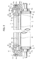
- Fig. 2 is a cross-sectional view of the photoconductive drum unit.
- Fig. 3 is a partial exploded perspective view illustrating a relationship of mounting members and a shield casing in a charging unit arranged in the photoconductive drum unit.
- An image forming device (A) illustrated in Fig. 1 is a printer including an electrophotographic printing unit as an example.
- the image forming device (A) is not limited to the illustrated example, and may be a copier, a facsimile machine, or an MFP including a copier function and/or a facsimile function including an image scanning device.
- a device main body 1 of the image forming device (A) includes a paper feeding unit 2 of printing papers (papers), an electrophotographic image printing unit 3, and a discharge unit 4 where printed papers are discharged.
- the paper feeding unit 2, the image printing unit 3, and the discharge unit 4 are vertically stacked in this order.
- the paper feeding unit 2 includes a paper feed cassette 2a, a paper separating and feeding roller 2b, and a separating pad 2c.
- the paper feed cassette 2a accommodates a plurality of stacked printing papers, and can be inserted and drawn out with respect to the device main body 1.
- the separating roller (pickup roller) 2b is arranged at a front end portion of the paper feed cassette 2a.
- the separating pad 2c elastically makes contact with a peripheral surface of the paper separating and feeding roller 2b.
- the paper feeding unit 2 is not limited to one cassette system as illustrated in Fig. 1 as an example, and may include a plurality of cassettes or adopt an interchangeable cassette system.
- the image printing unit 3 includes a process portion and a fusing unit 11 arranged downstream of the process portion.
- a charging unit 6, an exposing unit 7 such as a Light Emitting Diode (LED), a developing device 8, a transfer roller 9, and a remaining toner removing device 10 are arranged in this order around a photoconductive drum 5.
- the process portion is provided as a process unit including a photoconductive drum unit 50 and a developing device unit 80.
- the photoconductive drum unit 50 collectively includes the photoconductive drum 5, the charging unit 6, and the remaining toner removing device 10.
- the developing device unit 80 collectively includes a toner container, an agitator, and a developing roller or the like.
- the photoconductive drum unit 50 and the developing device unit 80 are removably inserted in the device main body 1 from its front surface side. Further, the photoconductive drum unit 50 and the developing device unit 80 may be inserted separately, or inserted in a state in which the photoconductive drum unit 50 and the developing device unit 80 are combined by a combining member. Alternatively, the entire process portion excluding the exposing unit 7 and the transfer roller 9 may be collectively provided as a process unit. Further, the front surface side of the device main body 1 refers to a front side in the page of Fig. 1, and an inner side of the page of Fig. 1 will be referred to as a rear surface side.
- a switching gate 4a, a discharge roller pair 4b, and a discharge tray 4c are arranged downstream of the fusing unit 11.
- the switching gate 4a, the discharge roller pair 4b, and the discharge tray 4c constitute the discharge unit 4.
- a resist roller pair 12 is arranged near an upstream side of the process portion.
- Printing papers (papers) accommodated in the paper feed cassette 2a are separated and picked up one sheet at a time by the paper separating and feeding roller 2b and the separating pad 2c, and resisted by the resist roller pair 12.
- the printing paper is introduced into a contact portion between the photoconductive drum 5 and the transfer roller 9.
- the photoconductive drum 5 rotates in a direction of an arrow illustrated in Fig. 1, and the surface of the photoconductive drum 5 is uniformly charged by the charging unit 6.
- An optical image based on image information is irradiated on the surface of the photoconductive drum 5 by the exposing unit 7. Accordingly, an electrostatic latent image is formed on the surface of the photoconductive drum 5. Further, the electrostatic latent image is formed according to characteristics of a photoconductor on the surface of the photoconductive drum 5, i.e., an electric potential of the irradiated portion changes while an electric potential of other portions is maintained.
- the electrostatic latent image is sequentially developed by the biased developing device 8, and reaches the contact portion between the photoconductive drum 5 and the transfer roller 9 as a toner image.
- a developing process according to a potential difference between the developing device 8 and the surface of the photoconductive drum 5, toner is adhered to the photoconductive drum 5 to form a black portion on a portion of the photoconductive drum 5 where the electric potential has changed by the irradiated light, and toner is not adhered to the remaining portion of the photoconductive drum 5 where a white portion is formed. Therefore, a black and white toner image according to image information is formed as a whole.
- the resist roller pair 12 is controlled to be rotatively driven such that printing paper is introduced into the contact portion between the photoconductive drum 5 and the transfer roller 9 in synchronism with the toner image formed on the surface of the photoconductive drum 5.
- a bias voltage is applied to the transfer roller 9.
- the transfer roller 9 is in contact with the photoconductive drum 5, and nips and transports printing paper while being rotatively driven in a direction illustrated by an arrow in Fig. 1 (in a with direction with the photoconductive drum 5).
- the toner image on the surface of the photoconductive drum 5 is transferred onto the printing paper.
- the toner remaining on the surface of the photoconductive drum 5 is removed by the remaining toner removing device 10 and collected.
- the printing paper on which the toner image has been transferred is introduced into the fusing unit 11. After the toner image is fixed as a permanent image, the printing paper pushes up the switching gate 4a, and is discharged onto the discharge tray 4c via the discharge roller pair 4b.
- the series of the paper feeding process is carried out along a main feeding path P.
- the main feeding path P rises substantially vertically (perpendicularly) immediately after the paper feed cassette 2a, and makes a U-turn at the discharge roller pair 4b in a direction substantially 180 degrees opposite from a direction in which printing paper is picked up from the paper feed cassette 2a.
- Such a layout structure downsizes the size of the image forming device (A) as a whole.
- the image forming device (A) includes a duplex printing function.
- a reversal feeding path P1 is bypassed and connects a position where the switching gate 4a is mounted and an upstream side of the resist roller pair 12 in the main feeding path P.
- the discharge roller pair 4b can rotate in both directions.
- Transportation roller pairs 13 and 14 are arranged in the reversal feeding path 21.
- the discharge roller pair 4b rotates backward, and the printing paper is transported through the reversal feeding path P1 by the transportation roller pairs 13 and 14 from its trailing edge.
- the printing paper eventually joins the main feeding path P and reaches the resist roller pair 12.
- the printing paper is resisted by the resist roller pair 12, and is introduced into the contact portion between the photoconductive drum 5 and the transfer roller 9 again.
- a printing operation is performed on a reverse side of the printing paper. After both sides of the printing paper are printed, the printing paper is transported along the main feeding path P and discharged onto the discharge tray 4c as described above.
- the image forming device (A) further includes a manual feeding function.
- a manual feeding tray 15 is arranged on a side of the device main body 1 in a manner that the manual feeding tray 15 can be opened and closed vertically. When not using the manual feeding tray 15, the manual feeding tray 15 is shut as illustrated by double-dashed lines in Fig. 1.
- the manual feeding tray 15 can be opened and closed by a gripper 15a.
- a paper separating and feeding roller 15b and a separating pad 15c are arranged contacting against one another at a front end portion of the manual feeding tray 15.
- a manual feeding path P2 is arranged downstream of such a contact portion, and joins with the main feeding path P.
- the gripper 15a When carrying out an image printing operation using the manual feeding tray 15, the gripper 15a is operated to open the manual feeding tray 15. Printing papers are set on the manual feeding tray 15, and after a start operation is performed, the manual feeding roller 15b starts operating. The printing papers stacked on the manual feeding tray 15 are separated and picked up one sheet at a time by the paper separating and feeding roller 15b and the separating pad 15c. The printing paper is transported along the manual feeding path P2, and joins the main feeding path P. Then, the printing paper is resisted by the resist roller pair 12, and introduced into the contact portion between the photoconductive drum 5 and the transfer roller 9 where a printing operation is performed.
- the discharge roller pair 4b rotates backward to transport the printing paper to the reversal feeding path P1, and the printing operation is performed on the reverse side of the printing paper as described above. After the printing operation is completed, the printing paper is discharged onto the discharge tray 4c by the discharge roller pair 4b.
- the photoconductive drum 5 includes an aluminum conductive cylindrical body. A photoconductor is coated on the surface of the cylindrical body. Flange members 5a and 5b are fixed on an opening at both ends of the cylindrical body. Further, the flange members 5a and 5b are insulating resin or plastic. The flange members 5a and 5b at both ends are supported on a unit frame 51 via bearings 51a and 51b, respectively. Further, the unit frame 51 is made of resin or plastic. The photoconductive drum 5 is supported rotatably on the unit frame 51 by the bearings 51a and 51b via the flange members 5a and 5b.
- the flange members 5a and 5b are respectively supported rotatably on drum shafts 1a and 1b fixed on a frame of the device main body 1.
- the drum shafts 1a and 1b also function as a positioning pin.
- Gears 5c and 5d are respectively formed concentrically on the surface of the flange members 5a and 5b.
- the gear 5c is engaged with a drive transmitting system (not illustrated) in the device main body 1.
- the photoconductive drum 5 rotates with the drum shafts 1a and 1b as a rotational axis by a driving force from the transmitting system.
- the gear 5d at an opposite side engages with a driven force transmitting gear of a mechanism portion (not illustrated) of the transfer roller 9 or the like. Accordingly, a rotational driving force is transmitted to the mechanism portion.
- the charging unit 6 is a scorotron charging unit.
- the charging unit 6 includes a pair of mounting members 61 and 62, a discharging electrode filament 63, a shield casing 64, and a grid 65.
- the mounting members 61 and 62, the discharging electrode filament 63, the shield casing 64, and the grid 65 are unitized to form the charging unit 6.
- the pair of the mounting members 61 and 62 are mounted and fixed on both end portions of the unit frame 51.
- the discharging electrode filament 63 is laid across under a tensioned state between the mounting members 61 and 62.
- the shield casing 64 is substantially U-shaped in its cross-section. The shield casing 64 is supported between the mounting members 61 and 62, and combined with the mounting members 61 and 62.
- the shield casing 64 covers the discharging electrode filament 63.
- the grid 65 is laid across under a tensioned state between the mounting members 61 and 62, and arranged in an opening 64a of the shield casing 64 at the photoconductive drum 5 side.
- the mounting members 61 and 62 are respectively fixed on the unit frame 51 by tightening screws 61b and 62b in screw holes 61a and 62a respectively formed on the mounting members 61 and 62.
- the discharging electrode filament 63 is a corona discharge electrode, and is formed of a thin band-like metal plate having a plurality of needle-like electrodes 63a as illustrated in Fig. 2.
- the discharging electrode filament 63 may be a metal wire.
- One end portion 63b of the discharging electrode filament 63 is caught in the mounting member 61.
- Another end portion 63c is caught in the other mounting member 62 via a tension spring 63d.
- the discharging electrode filament 63 is laid across under a tensioned state between the mounting members 61 and 62.
- the grid 65 is a thin metal plate on which a plurality of slits are formed.
- One end 65a of the grid 65 is caught in the mounting member 61.
- Another end 65b is caught in the mounting member 62 via a swinging portion 65c and a tension spring (spring member) 65d.
- the swinging portion 65c is arranged to penetrate through the mounting member 62 from the photoconductive drum 5 side to its opposite side. At the same time, the swinging portion 65c is supported capable of swinging around a supporting pin 65ca. The other end 65b of the grid 65 is caught on a protruding end portion of the swinging portion 65c at the photoconductive drum 5 side. The tension spring 65d is caught in another protruding end portion of the swinging portion 65c at the opposite side.
- the shield casing 64 having a substantially U-shape in its cross-section is arranged such that its opening 64a faces towards the photoconductive drum 5 side.
- the grid 65 is located in the opening 64a of the shield casing 64.
- the grid 65 is tensioned by a pulling force of the tension spring 65d via the swinging portion 65c, and is laid across under a tensioned state between the mounting members 61 and 62.
- the discharging electrode filament 63 and the grid 65 make contact with a power electrode (not illustrated) in the device main body 1.
- a prescribed voltage can be applied to each of the discharging electrode filament 63 and the grid 65.
- Fig. 3 is an exploded perspective view illustrating a relationship of how the mounting members 61 and 62 are combined with the shield casing 64. Further, the discharging electrode filament 63 and the grid 65 are not illustrated in Fig. 3.
- a plurality of catching pins 60a protrude from side surfaces of the mounting members 61 and 62 and from a surface of the mounting members 61 and 62 located opposite from the photoconductive drum 5 side. Meanwhile, a plurality of catching holes 60b are formed on the shield casing 64 at positions corresponding to the catching pins 60a.
- a diameter of the catching holes 60b is slightly larger than a diameter of the catching pins 60a, or the catching holes 60b are oval.
- the combining members 60 are formed by the catching pins 60a being caught in the catching holes 60b.
- the catching pins 60a and the catching holes 60b are formed such that when the catching pins 60a are caught in the catching holes 60b, the catching pins 60a are loosely fit in the catching holes 60b.
- the mounting members 61 and 62 and the shield casing 64 are combined by inserting and catching the catching pins 60a in the catching holes 60b. Since the catching holes 60a have a larger diameter than the catching pins 60b or are oval, the catching pins 60a are loosely caught in the catching holes 60b. As a result, the mounting members 61 and 62 and the shield casing 64 combined by the combining members 60 permit a slight displacement. Under such combined state of the mounting members 61 and 62 and the shield casing 64, as described above, the discharging electrode filament 63 and the grid 65 are respectively laid across under a tensioned state between the mounting members 61 and 62 by being tensioned by the tension springs 63d and 65d, respectively.
- the mounting members 61 and 62 are fixed on the unit frame 51 by tightening the screws 61b and 62b, when assembling the charging unit 6 in the photoconductive drum unit 50, for example, even if the unit frame 51 is distorted, a restriction of the shield casing 64 is small and the mounting members 61 and 62 can respond to the unit frame 51. Therefore, the mounting members 61 and 62 can be fixed reliably. Since the discharging electrode filament 63 and the grid 65 are laid across under a tensioned state between the mounting members 61 and 62, an initial relative positional relationship of the discharging electrode filament 63 and the grid 65 does not change. Furthermore, a relative distance between the grid 65 and the surface of the photoconductive drum 5 in its longitudinal direction is maintained substantially constant.
- the mounting members 61 and 62 respond to the distortion of the unit frame 51.
- the grid 65 is always maintained under a tensioned state, and the relative distance between the grid 65 and the surface of the photoconductive drum 5 can be reliably kept constant.
- the distortion or the like of the unit frame 51 can be responded by a simple structure, i.e., the combining members 60 including the catching holes 60b and the catching pins 60a, and the grid 65, which is provided under a tensioned state.
- a constant distance can be maintained between the grid 65 and the surface of the photoconductive drum 5.
- charge unevenness can be prevented in the longitudinal direction of the photoconductive drum 5, and deterioration in an image quality can be prevented.
- the shape of the shield casing 64 of the charging unit 6, the overall shape of the mounting members 61 and 62 are not limited to the illustrated examples.
- a resin or plastic film may be adhered like a skirt on a side portion of the shield casing.
- the shape of the catching pins 60a and the catching holes 60b of the combining member 60 is also not limited to a cylindrical pin or a circular hole as illustrated in the drawings.
- the catching pins 60a and the catching holes 60b may be a prism pin and a rectangular hole, or formed in any other shape.
- the catching pins 60a may be formed on the shield casing 64, and the catching holes 60b may be formed on the mounting members 61 and 62.
Landscapes
- Physics & Mathematics (AREA)
- Engineering & Computer Science (AREA)
- Plasma & Fusion (AREA)
- General Physics & Mathematics (AREA)
- Electrostatic Charge, Transfer And Separation In Electrography (AREA)
Abstract
Description
- The present invention relates to a photoconductive drum unit which constitutes an electrophotographic image forming device. The image forming device may be incorporated in a facsimile machine, a copier, or a printer or the like (including a Multi Function Peripheral (MFP) of the facsimile machine, the copier, and/or the printer). More specifically, the present invention relates to a photoconductive drum unit including a scorotron charging unit.
- In the electrophotographic image forming device, a photoconductive drum is rotatably supported on a unit frame. A scorotron charging unit is mounted and fixed on the unit frame in a manner that the scorotron charging unit is arranged facing a surface of the photoconductive drum and along a longitudinal direction of the photoconductive drum. The unitized photoconductive drum unit is widely adopted. In such a scorotron charging method, when a distance between the surface of the photoconductive drum and a grid is not maintained at an equal distance at any position in the longitudinal direction of the photoconductive drum, charge unevenness generates in the longitudinal direction of the photoconductive drum and influences an image quality.
- In a conventional charging unit, a shield casing, a discharge wire (filament) and a grid are integrally assembled as one unit. The charging unit is fixed on a unit frame by tightening screws at both ends of the unit frame in its longitudinal direction. Further, the unit frame supports a photoconductive drum. Since the unit frame is made of resin or plastic, the unit frame may be twisted or distorted in its longitudinal direction. Meanwhile, since the charging unit is formed as a solid singular body as a whole, when the charging unit is fixed onto the unit frame by tightening the screws, it is difficult for the charging unit to respond to the distortion of the unit frame. Thus, there has been a problem that a distance between the grid and the surface of the photoconductive drum is not constant in the longitudinal direction.
- According to one conventional art, a scorotron charging unit includes a holding member that holds a grid plate on a shaft of a photoconductor. In such a charging unit, there has been a problem that a distance between the surface of the photoconductor and the grid plate changes according to a degree of eccentricity of the shaft. Therefore, according to a conventionally proposed scorotron charging unit, a positioning member is provided for maintaining a prescribed distance between the surface of the photoconductor and the grid plate by making contact with the surface of the photoconductor. The positioning member applies tension to the grid plate in its longitudinal direction. According to another conventional art, a grid electrode is provided separately from a main body of a charging device. The grid electrode is supported via a positioning member and a position adjusting device with respect to a photoconductor supporting body (unit frame), which rotatably supports a photoconductive drum.
- In the conventionally proposed scorotron charging unit, the charging unit is supported between holders that are fixedly mounted on the unit frame. Accordingly, since the holding members of the grid plate are positioned by the positioning member making contact with the surface of the photoconductor, a prescribed interval can be maintained between the grid plate and the photoconductor. However, since the positioning member is required to be coated with a low-friction material such as Teflon (registered trademark), an increase in costs was inevitable. Moreover, since the holders fixedly mounted on the unit frame are integrally formed with the charging unit, the charging unit and the unit frame are formed as one solid body as a whole. Therefore, even when the unit frame is distorted, it is difficult for the charging unit to respond to such distortion. As a result, it is also difficult to reliably mount and fix the charging unit in such a situation.
- According to another proposed charging device, a grid electrode is provided separately from a charging device main body, and is mounted on a unit frame of a photoconductive drum. According to this structure, since a positioning member and a position adjusting device are required, a number of components increases causing an increase in costs. Furthermore, since the grid electrode is mounted on the unit frame, when the charging device and the photoconductive drum are formed as a drum unit, it becomes necessary to adjust the position of the charging device main body and the grid electrode.
- In order to overcome the problems described above, according to preferred embodiments of the present invention, a charging unit responds to distortion or the like of a unit frame to enable a prescribed positional relationship to be maintained between the charging unit and a photoconductive drum under a simple structure.
- According to a preferred aspect of the present invention, a photoconductive drum unit includes a unit frame, a photoconductive drum, and a scorotron charging unit. The photoconductive drum is supported rotatably on the unit frame. The scorotron charging unit is arranged facing a surface of the photoconductive drum, and fixedly mounted on both end portions of the unit frame along its longitudinal direction. The charging unit includes a pair of mounting members, a discharging electrode filament, a shield casing, a grid, and a combining member. The pair of the mounting members is fixedly mounted on both end portions of the unit frame. The discharging electrode filament is laid across in a tensioned state between the mounting members. The shield casing is supported between the mounting members by being combined with the mounting members, and covers the discharging electrode filament. The grid is laid across in a tensioned state between the mounting members, and is arranged in an opening in the shield casing at the photoconductive drum side. The pair of the mounting members and the shield casing are combined via the combining members so as to permit a slight displacement of the mounting members and the shield casing with respect to one another.
- According to another preferred aspect of the invention, the combining member includes a catching pin and a catching hole formed on the mounting members and the shield casing. The catching pin and the catching hole are formed such that when the catching pin is inserted in the catching hole, the catching pin is loosely fit in the catching hole. The grid is preferably laid across in a tensioned state in its longitudinal direction between the mounting members via a spring member.
- According to a further preferred aspect of the invention, the mounting members arranged at both end portions of the charging unit and the shield casing, which constitute the charging unit, are combined via the combining member that permits a slight displacement of the mounting members and the shield casing. Therefore, when mounting the mounting members to the unit frame, even when the unit frame is distorted by being twisted in the longitudinal direction, each of the mounting members respond to the distortion. As a result, the mounting members can be mounted and fixed reliably. Moreover, since the grid is laid across in a tensioned state between the mounting members and is arranged in the opening of the shield casing at the photoconductive drum side, the distance between the grid and the surface of the photoconductive drum is maintained at a prescribed distance along the longitudinal direction. As a result, charge unevenness is not generated. Furthermore, since the discharging electrode filament is also laid across in a tensioned state between the mounting members, the discharging electrode filament and the grid are maintained under a prescribed relative positional relationship. The reliability of mounting the charging unit on the unit frame, and the response of the grid with respect to the unit frame are accomplished by the mounting members and the shield casing being combined via the combining member that permits a slight displacement between the mounting members and the shield casing. As a result, just a simple structure can be required, and an increase in a number of components and an increase in costs can be prevented.
- According to one of the above-described preferred aspects of the present invention, the combining member includes the catching pin and the catching hole formed on the mounting members and the shield. The catching pin and the catching hole are formed such that when the catching pin is inserted in the catching hole, the catching pin is loosely fit in the catching hole. As a result, reliability of mounting and the response of the grid with respect to the unit frame can be accomplished extremely easily. According to yet another preferred aspect of the invention, the grid is laid across in a tensioned state in its longitudinal direction via the spring member with respect to the mounting members. Therefore, the grid is always maintained under a tensioned state. In addition, since the mounting members can be mounted reliably in response to the unit frame, a prescribed distance can be reliably maintained between the grid and the surface of the photoconductive drum.
- Other features, elements, processes, steps, characteristics and advantages of the present invention will become more apparent from the following detailed description of preferred embodiments of the present invention with reference to the attached drawings.
- Fig. 1 is a longitudinal cross-sectional view of an example of an image forming device including a photoconductive drum unit according to a preferred embodiment of the present invention.
- Fig. 2 is a cross-sectional view of the photoconductive drum unit.
- Fig. 3 is a partial exploded perspective view illustrating a relationship of mounting members and a shield casing in a charging unit arranged in the photoconductive drum unit.
- Preferred embodiments of the present invention will be described with reference to the accompanying drawings.
- An image forming device (A) illustrated in Fig. 1 is a printer including an electrophotographic printing unit as an example. The image forming device (A) is not limited to the illustrated example, and may be a copier, a facsimile machine, or an MFP including a copier function and/or a facsimile function including an image scanning device. In Fig. 1, a device
main body 1 of the image forming device (A) includes apaper feeding unit 2 of printing papers (papers), an electrophotographic image printing unit 3, and adischarge unit 4 where printed papers are discharged. Thepaper feeding unit 2, the image printing unit 3, and thedischarge unit 4 are vertically stacked in this order. Thepaper feeding unit 2 includes apaper feed cassette 2a, a paper separating and feedingroller 2b, and aseparating pad 2c. Thepaper feed cassette 2a accommodates a plurality of stacked printing papers, and can be inserted and drawn out with respect to the devicemain body 1. The separating roller (pickup roller) 2b is arranged at a front end portion of thepaper feed cassette 2a. Theseparating pad 2c elastically makes contact with a peripheral surface of the paper separating and feedingroller 2b. Thepaper feeding unit 2 is not limited to one cassette system as illustrated in Fig. 1 as an example, and may include a plurality of cassettes or adopt an interchangeable cassette system. - The image printing unit 3 includes a process portion and a
fusing unit 11 arranged downstream of the process portion. In the process portion, a chargingunit 6, an exposing unit 7 such as a Light Emitting Diode (LED), a developingdevice 8, a transfer roller 9, and a remainingtoner removing device 10 are arranged in this order around a photoconductive drum 5. Excluding the exposing unit 7 and the transfer roller 9, the process portion is provided as a process unit including aphotoconductive drum unit 50 and a developingdevice unit 80. Further, thephotoconductive drum unit 50 collectively includes the photoconductive drum 5, the chargingunit 6, and the remainingtoner removing device 10. The developingdevice unit 80 collectively includes a toner container, an agitator, and a developing roller or the like. Thephotoconductive drum unit 50 and the developingdevice unit 80 are removably inserted in the devicemain body 1 from its front surface side. Further, thephotoconductive drum unit 50 and the developingdevice unit 80 may be inserted separately, or inserted in a state in which thephotoconductive drum unit 50 and the developingdevice unit 80 are combined by a combining member. Alternatively, the entire process portion excluding the exposing unit 7 and the transfer roller 9 may be collectively provided as a process unit. Further, the front surface side of the devicemain body 1 refers to a front side in the page of Fig. 1, and an inner side of the page of Fig. 1 will be referred to as a rear surface side. - A switching
gate 4a, adischarge roller pair 4b, and a discharge tray 4c are arranged downstream of the fusingunit 11. The switchinggate 4a, thedischarge roller pair 4b, and the discharge tray 4c constitute thedischarge unit 4. A resistroller pair 12 is arranged near an upstream side of the process portion. Printing papers (papers) accommodated in thepaper feed cassette 2a are separated and picked up one sheet at a time by the paper separating and feedingroller 2b and theseparating pad 2c, and resisted by the resistroller pair 12. The printing paper is introduced into a contact portion between the photoconductive drum 5 and the transfer roller 9. The photoconductive drum 5 rotates in a direction of an arrow illustrated in Fig. 1, and the surface of the photoconductive drum 5 is uniformly charged by the chargingunit 6. An optical image based on image information is irradiated on the surface of the photoconductive drum 5 by the exposing unit 7. Accordingly, an electrostatic latent image is formed on the surface of the photoconductive drum 5. Further, the electrostatic latent image is formed according to characteristics of a photoconductor on the surface of the photoconductive drum 5, i.e., an electric potential of the irradiated portion changes while an electric potential of other portions is maintained. - The electrostatic latent image is sequentially developed by the biased developing
device 8, and reaches the contact portion between the photoconductive drum 5 and the transfer roller 9 as a toner image. During a developing process, according to a potential difference between the developingdevice 8 and the surface of the photoconductive drum 5, toner is adhered to the photoconductive drum 5 to form a black portion on a portion of the photoconductive drum 5 where the electric potential has changed by the irradiated light, and toner is not adhered to the remaining portion of the photoconductive drum 5 where a white portion is formed. Therefore, a black and white toner image according to image information is formed as a whole. The resistroller pair 12 is controlled to be rotatively driven such that printing paper is introduced into the contact portion between the photoconductive drum 5 and the transfer roller 9 in synchronism with the toner image formed on the surface of the photoconductive drum 5. - A bias voltage is applied to the transfer roller 9. The transfer roller 9 is in contact with the photoconductive drum 5, and nips and transports printing paper while being rotatively driven in a direction illustrated by an arrow in Fig. 1 (in a with direction with the photoconductive drum 5). At this time, the toner image on the surface of the photoconductive drum 5 is transferred onto the printing paper. The toner remaining on the surface of the photoconductive drum 5 is removed by the remaining
toner removing device 10 and collected. The printing paper on which the toner image has been transferred is introduced into the fusingunit 11. After the toner image is fixed as a permanent image, the printing paper pushes up the switchinggate 4a, and is discharged onto the discharge tray 4c via thedischarge roller pair 4b. The series of the paper feeding process is carried out along a main feeding path P. The main feeding path P rises substantially vertically (perpendicularly) immediately after thepaper feed cassette 2a, and makes a U-turn at thedischarge roller pair 4b in a direction substantially 180 degrees opposite from a direction in which printing paper is picked up from thepaper feed cassette 2a. Such a layout structure downsizes the size of the image forming device (A) as a whole. - The image forming device (A) includes a duplex printing function. A reversal feeding path P1 is bypassed and connects a position where the switching
gate 4a is mounted and an upstream side of the resistroller pair 12 in the main feeding path P. Thedischarge roller pair 4b can rotate in both directions. Transportation roller pairs 13 and 14 are arranged in the reversal feeding path 21. When carrying out a duplex printing operation, after one side of the printing paper is printed as described above, the printing paper is transported along the main feeding path P, and when a trailing edge of the printing paper reaches thedischarge roller pair 4b, thedischarge roller pair 4b stops once to temporarily nip the trailing edge of the printing paper. Next, thedischarge roller pair 4b rotates backward, and the printing paper is transported through the reversal feeding path P1 by the transportation roller pairs 13 and 14 from its trailing edge. The printing paper eventually joins the main feeding path P and reaches the resistroller pair 12. The printing paper is resisted by the resistroller pair 12, and is introduced into the contact portion between the photoconductive drum 5 and the transfer roller 9 again. A printing operation is performed on a reverse side of the printing paper. After both sides of the printing paper are printed, the printing paper is transported along the main feeding path P and discharged onto the discharge tray 4c as described above. - The image forming device (A) further includes a manual feeding function. A
manual feeding tray 15 is arranged on a side of the devicemain body 1 in a manner that themanual feeding tray 15 can be opened and closed vertically. When not using themanual feeding tray 15, themanual feeding tray 15 is shut as illustrated by double-dashed lines in Fig. 1. Themanual feeding tray 15 can be opened and closed by agripper 15a. A paper separating and feedingroller 15b and aseparating pad 15c are arranged contacting against one another at a front end portion of themanual feeding tray 15. A manual feeding path P2 is arranged downstream of such a contact portion, and joins with the main feeding path P. - When carrying out an image printing operation using the
manual feeding tray 15, thegripper 15a is operated to open themanual feeding tray 15. Printing papers are set on themanual feeding tray 15, and after a start operation is performed, themanual feeding roller 15b starts operating. The printing papers stacked on themanual feeding tray 15 are separated and picked up one sheet at a time by the paper separating and feedingroller 15b and theseparating pad 15c. The printing paper is transported along the manual feeding path P2, and joins the main feeding path P. Then, the printing paper is resisted by the resistroller pair 12, and introduced into the contact portion between the photoconductive drum 5 and the transfer roller 9 where a printing operation is performed. When carrying out a duplex printing operation on the manually fed paper, thedischarge roller pair 4b rotates backward to transport the printing paper to the reversal feeding path P1, and the printing operation is performed on the reverse side of the printing paper as described above. After the printing operation is completed, the printing paper is discharged onto the discharge tray 4c by thedischarge roller pair 4b. - Next, with reference to Fig. 2 and Fig. 3, a detailed description will be made of the
photoconductive drum unit 50. The photoconductive drum 5 includes an aluminum conductive cylindrical body. A photoconductor is coated on the surface of the cylindrical body.Flange members flange members flange members unit frame 51 viabearings unit frame 51 is made of resin or plastic. The photoconductive drum 5 is supported rotatably on theunit frame 51 by thebearings flange members flange members drum shafts main body 1. Thedrum shafts Gears 5c and 5d are respectively formed concentrically on the surface of theflange members gear 5c is engaged with a drive transmitting system (not illustrated) in the devicemain body 1. The photoconductive drum 5 rotates with thedrum shafts - The charging
unit 6 is a scorotron charging unit. The chargingunit 6 includes a pair of mountingmembers electrode filament 63, ashield casing 64, and agrid 65. The mountingmembers electrode filament 63, theshield casing 64, and thegrid 65 are unitized to form thecharging unit 6. The pair of the mountingmembers unit frame 51. The dischargingelectrode filament 63 is laid across under a tensioned state between the mountingmembers shield casing 64 is substantially U-shaped in its cross-section. Theshield casing 64 is supported between the mountingmembers members shield casing 64 covers the dischargingelectrode filament 63. Thegrid 65 is laid across under a tensioned state between the mountingmembers opening 64a of theshield casing 64 at the photoconductive drum 5 side. The mountingmembers unit frame 51 by tighteningscrews screw holes members - The discharging
electrode filament 63 is a corona discharge electrode, and is formed of a thin band-like metal plate having a plurality of needle-like electrodes 63a as illustrated in Fig. 2. The dischargingelectrode filament 63 may be a metal wire. Oneend portion 63b of the dischargingelectrode filament 63 is caught in the mountingmember 61. Anotherend portion 63c is caught in the other mountingmember 62 via atension spring 63d. As described above, the dischargingelectrode filament 63 is laid across under a tensioned state between the mountingmembers grid 65 is a thin metal plate on which a plurality of slits are formed. Oneend 65a of thegrid 65 is caught in the mountingmember 61. Anotherend 65b is caught in the mountingmember 62 via a swingingportion 65c and a tension spring (spring member) 65d. - The swinging
portion 65c is arranged to penetrate through the mountingmember 62 from the photoconductive drum 5 side to its opposite side. At the same time, the swingingportion 65c is supported capable of swinging around a supporting pin 65ca. Theother end 65b of thegrid 65 is caught on a protruding end portion of the swingingportion 65c at the photoconductive drum 5 side. Thetension spring 65d is caught in another protruding end portion of the swingingportion 65c at the opposite side. Theshield casing 64 having a substantially U-shape in its cross-section is arranged such that itsopening 64a faces towards the photoconductive drum 5 side. Thegrid 65 is located in theopening 64a of theshield casing 64. Thegrid 65 is tensioned by a pulling force of thetension spring 65d via the swingingportion 65c, and is laid across under a tensioned state between the mountingmembers photoconductive drum unit 50 is inserted in a prescribed portion in the image forming device (A), the dischargingelectrode filament 63 and thegrid 65 make contact with a power electrode (not illustrated) in the devicemain body 1. A prescribed voltage can be applied to each of the dischargingelectrode filament 63 and thegrid 65. - The mounting
members shield casing 64 are combined via combiningmembers 60. A further description will be made with reference to Fig. 3. Fig. 3 is an exploded perspective view illustrating a relationship of how the mountingmembers shield casing 64. Further, the dischargingelectrode filament 63 and thegrid 65 are not illustrated in Fig. 3. A plurality of catchingpins 60a protrude from side surfaces of the mountingmembers members holes 60b are formed on theshield casing 64 at positions corresponding to the catchingpins 60a. Further, a diameter of the catchingholes 60b is slightly larger than a diameter of the catchingpins 60a, or the catchingholes 60b are oval. The combiningmembers 60 are formed by the catchingpins 60a being caught in the catchingholes 60b. The catching pins 60a and the catchingholes 60b are formed such that when the catchingpins 60a are caught in the catchingholes 60b, the catchingpins 60a are loosely fit in the catchingholes 60b. - The mounting
members shield casing 64 are combined by inserting and catching the catchingpins 60a in the catchingholes 60b. Since the catchingholes 60a have a larger diameter than the catchingpins 60b or are oval, the catchingpins 60a are loosely caught in the catchingholes 60b. As a result, the mountingmembers shield casing 64 combined by the combiningmembers 60 permit a slight displacement. Under such combined state of the mountingmembers shield casing 64, as described above, the dischargingelectrode filament 63 and thegrid 65 are respectively laid across under a tensioned state between the mountingmembers - Since the mounting
members unit frame 51 by tightening thescrews unit 6 in thephotoconductive drum unit 50, for example, even if theunit frame 51 is distorted, a restriction of theshield casing 64 is small and the mountingmembers unit frame 51. Therefore, the mountingmembers electrode filament 63 and thegrid 65 are laid across under a tensioned state between the mountingmembers electrode filament 63 and thegrid 65 does not change. Furthermore, a relative distance between thegrid 65 and the surface of the photoconductive drum 5 in its longitudinal direction is maintained substantially constant. In addition, since the dischargingelectrode filament 63 and thegrid 65 are laid across under a tensioned state by the tension springs 63d and 65d, the mountingmembers unit frame 51. As a result, even when thegrid 65 is relatively displaced with respect to theshield casing 64, thegrid 65 is always maintained under a tensioned state, and the relative distance between thegrid 65 and the surface of the photoconductive drum 5 can be reliably kept constant. - As described above, the distortion or the like of the
unit frame 51 can be responded by a simple structure, i.e., the combiningmembers 60 including the catchingholes 60b and the catchingpins 60a, and thegrid 65, which is provided under a tensioned state. In addition, a constant distance can be maintained between thegrid 65 and the surface of the photoconductive drum 5. As a result, charge unevenness can be prevented in the longitudinal direction of the photoconductive drum 5, and deterioration in an image quality can be prevented. - Further, the shape of the
shield casing 64 of the chargingunit 6, the overall shape of the mountingmembers pins 60a and the catchingholes 60b of the combiningmember 60 is also not limited to a cylindrical pin or a circular hole as illustrated in the drawings. For example, the catchingpins 60a and the catchingholes 60b may be a prism pin and a rectangular hole, or formed in any other shape. The catchingpins 60a may be formed on theshield casing 64, and the catchingholes 60b may be formed on the mountingmembers - While the present invention has been described with respect to preferred embodiments thereof, it will be apparent to those skilled in the art that the disclosed invention may be modified in numerous ways and may assume many embodiments other than those specifically set out and described above. Accordingly, the appended claims are intended to cover all modifications of the present invention that fall within the true scope of the present invention.
Claims (12)
- A scorotron charging device (6) mounted on a frame (51), the charging device (6) comprising a pair of mounting members (61, 62) mounted and fixed on both end portions of the frame (51), a discharging electrode filament (63) laid across under a tensioned state between the mounting members (61, 62), a shield casing (64) arranged to cover the discharging electrode filament (63) by being supported between the mounting members (61, 62) and combined with the mounting members (61, 62), and a grid (65) laid across under a tensioned state between the mounting members (61, 62) and arranged in an opening of the shield casing (64),
the charging device (6) including a combining means (60) for combining the pair of mounting members (61, 62) and the shield casing (64) in a state in which a slight displacement between the mounting members (61, 62) and the shield casing (64) is permitted. - A charging device (6) according to claim 1, wherein the combining means (60) includes a catching pin (60a) and a catching hole (60b), which are formed on the mounting members (61, 62) and the shield casing (64) and loosely caught with one another.
- A charging device (6) according to claim 1 or 2, including a spring (65d) which places the grid (65) in a state in which the grid (65) is tensioned in its longitudinal direction with respect to the mounting members (61, 62).
- A charging device according to any preceding claim, wherein the discharging electrode filament (63) is a thin band-shaped metal plate including a plurality of needle-like electrodes (63a).
- A photoconductive drum unit (50) comprising a frame (51), a photoconductive drum (5) rotatably supported on the frame (51), and a scorotron charging unit (6) which is arranged facing a surface of the photoconductive drum (5) and mounted and fixed at both end portions of the frame (51) to be provided along a longitudinal direction of the photoconductive drum (5),
wherein the charging unit (6) includes a pair of mounting members (61, 62) mounted and fixed on the end portions of the frame (51), a discharging electrode filament (63) laid across under a tensioned state between the mounting members (61, 62), a shield casing (64) arranged to cover the discharging electrode filament (63) by being supported between the mounting members (61, 62) and combined with the mounting members (61, 62), and a grid (65) laid across in a tensioned state between the mounting members (61, 62) and arranged in an opening of the shield casing (64),
the photoconductive drum unit (50) including a combining means (60) for combining the pair of mounting members (61, 62) and the shield casing (64) in a state in which a slight displacement between the mounting members (61, 62) and the shield casing (64) is permitted. - A photoconductive drum unit (50) according to claim 5, wherein the combining means (60) includes a catching pin (60a) and a catching hole (60b), which are formed on the mounting members (61, 62) and the shield casing (64) and loosely caught with one another.
- A photoconductive drum unit (50) according to claim 5 or 6, including a spring (65d) which places the grid (65) in a state in which the grid (65) is tensioned in its longitudinal direction with respect to the mounting members (61, 62).
- A photoconductive drum unit (50) according to any of claims 5 to 7, wherein the discharging electrode filament (63) is a thin band-shaped metal plate including a plurality of needle-like electrodes (63a).
- An image forming device (A) comprising a photoconductive drum unit (5) including a photoconductive drum (5) and a charging unit (6), and a developing device unit (80) which includes a toner container and a developing roller,
wherein the photoconductive drum unit (50) includes a frame (51), the photoconductive drum (5) is rotatably supported on the frame (51), and a scorotron charging unit (6) which is arranged facing a surface of the photoconductive drum (5) and mounted and fixed at both end portions of the frame (51) to be provided along a longitudinal direction of the photoconductive drum (5),
wherein the charging unit (6) includes a pair of mounting members (61, 62) mounted and fixed on the end portions of the frame (51), a discharging electrode filament (63) laid across in a tensioned state between the mounting members (61, 62), a shield casing (64) arranged to cover the discharging electrode filament (63) by being supported between the mounting members (61, 62) and combined with the mounting members(61, 62), and a grid (65) laid across in a tensioned state between the mounting members (61, 62) and arranged in an opening of the shield casing (64),
the image forming device (A) including a combing means (60) for combining the pair of mounting members (61, 62) and the shield casing (64) in a state in which a slight displacement between the mounting members (61, 62) and the shield casing (64) is permitted. - An image forming device (A) according to claim 9, wherein that the combining means (60) includes a catching pin (60a) and a catching hole (60b), which are formed on the mounting members (61, 62) and the shield casing (64) and loosely caught with one another.
- An image forming device (A) according to claim 9 or 10, including a spring (65d) which places the grid (65) in a state in which the grid (65) is tensioned in its longitudinal direction with respect to the mounting members (61, 62).
- An image forming device (A) according to any of claims 9 to 11, wherein the discharging electrode filament (63) is a thin band-shaped metal plate including a plurality of needle-like electrodes (63a).
Applications Claiming Priority (1)
| Application Number | Priority Date | Filing Date | Title |
|---|---|---|---|
| JP2006080854A JP4682891B2 (en) | 2006-03-23 | 2006-03-23 | Photosensitive drum unit |
Publications (1)
| Publication Number | Publication Date |
|---|---|
| EP1837711A1 true EP1837711A1 (en) | 2007-09-26 |
Family
ID=38198251
Family Applications (1)
| Application Number | Title | Priority Date | Filing Date |
|---|---|---|---|
| EP20070103027 Withdrawn EP1837711A1 (en) | 2006-03-23 | 2007-02-26 | Charging device, photoconductive drum unit, and image forming device |
Country Status (5)
| Country | Link |
|---|---|
| US (1) | US7570902B2 (en) |
| EP (1) | EP1837711A1 (en) |
| JP (1) | JP4682891B2 (en) |
| KR (1) | KR100984759B1 (en) |
| CN (1) | CN101042551B (en) |
Families Citing this family (6)
| Publication number | Priority date | Publication date | Assignee | Title |
|---|---|---|---|---|
| US8126367B2 (en) * | 2008-09-30 | 2012-02-28 | Xerox Corporation | Scorotron apparatus for charging a photoconductor |
| JP2011123419A (en) * | 2009-12-14 | 2011-06-23 | Konica Minolta Business Technologies Inc | Charger and image forming apparatus with the same |
| JP4802290B1 (en) * | 2010-06-02 | 2011-10-26 | シャープ株式会社 | Charging device and image forming apparatus |
| JP5315321B2 (en) * | 2010-11-11 | 2013-10-16 | 京セラドキュメントソリューションズ株式会社 | Charging device and image forming apparatus having the same |
| JP5849404B2 (en) * | 2011-02-16 | 2016-01-27 | 富士ゼロックス株式会社 | Image forming apparatus |
| JP6699625B2 (en) * | 2017-05-31 | 2020-05-27 | 京セラドキュメントソリューションズ株式会社 | Joint mechanism and image forming apparatus including the same |
Citations (4)
| Publication number | Priority date | Publication date | Assignee | Title |
|---|---|---|---|---|
| US3908127A (en) * | 1973-12-21 | 1975-09-23 | Xerox Corp | Corona generating devices |
| JPH01113249U (en) * | 1988-01-25 | 1989-07-31 | ||
| JPH03223773A (en) * | 1990-01-30 | 1991-10-02 | Ricoh Co Ltd | Corona discharger |
| US5909608A (en) * | 1998-01-07 | 1999-06-01 | Xerox Corporation | Tension support mounting for a corona generating device |
Family Cites Families (10)
| Publication number | Priority date | Publication date | Assignee | Title |
|---|---|---|---|---|
| JPS58159545U (en) * | 1982-04-20 | 1983-10-24 | オリンパス光学工業株式会社 | corona charger |
| JPS62143961U (en) * | 1986-03-04 | 1987-09-10 | ||
| JP2732657B2 (en) * | 1989-04-10 | 1998-03-30 | 株式会社リコー | Corona charging device |
| US5216465A (en) * | 1990-03-19 | 1993-06-01 | Fuji Xerox Co., Ltd. | Print cartridge insertable into an image forming apparatus |
| JP2861252B2 (en) * | 1990-05-11 | 1999-02-24 | 富士ゼロックス株式会社 | Scorotron charger grid plate positioning device |
| JPH0529481Y2 (en) | 1990-10-11 | 1993-07-28 | ||
| JPH04133258U (en) | 1991-05-29 | 1992-12-11 | ミノルタカメラ株式会社 | Scorotron type charger |
| JPH0635296A (en) | 1992-07-17 | 1994-02-10 | Fuji Xerox Co Ltd | Electrostatic charging device for image forming device |
| JP3304209B2 (en) * | 1994-09-14 | 2002-07-22 | シャープ株式会社 | Charging device |
| JPH0980998A (en) * | 1995-09-13 | 1997-03-28 | Tec Corp | Image forming device |
-
2006
- 2006-03-23 JP JP2006080854A patent/JP4682891B2/en not_active Expired - Fee Related
-
2007
- 2007-02-09 KR KR1020070013722A patent/KR100984759B1/en not_active Expired - Fee Related
- 2007-02-25 CN CN2007100058500A patent/CN101042551B/en not_active Expired - Fee Related
- 2007-02-26 EP EP20070103027 patent/EP1837711A1/en not_active Withdrawn
- 2007-03-05 US US11/681,904 patent/US7570902B2/en not_active Expired - Fee Related
Patent Citations (4)
| Publication number | Priority date | Publication date | Assignee | Title |
|---|---|---|---|---|
| US3908127A (en) * | 1973-12-21 | 1975-09-23 | Xerox Corp | Corona generating devices |
| JPH01113249U (en) * | 1988-01-25 | 1989-07-31 | ||
| JPH03223773A (en) * | 1990-01-30 | 1991-10-02 | Ricoh Co Ltd | Corona discharger |
| US5909608A (en) * | 1998-01-07 | 1999-06-01 | Xerox Corporation | Tension support mounting for a corona generating device |
Also Published As
| Publication number | Publication date |
|---|---|
| KR100984759B1 (en) | 2010-10-01 |
| US20070223961A1 (en) | 2007-09-27 |
| JP2007256629A (en) | 2007-10-04 |
| KR20070096794A (en) | 2007-10-02 |
| CN101042551B (en) | 2011-03-23 |
| CN101042551A (en) | 2007-09-26 |
| US7570902B2 (en) | 2009-08-04 |
| JP4682891B2 (en) | 2011-05-11 |
Similar Documents
| Publication | Publication Date | Title |
|---|---|---|
| US6163666A (en) | Process cartridge and an image forming apparatus using the same process cartridge and a method of manufacturing the same process cartridge | |
| US9690246B2 (en) | Image forming apparatus including contact members disposed side by side at positions opposing a guide unit | |
| US7570902B2 (en) | Charging device, photoconductive drum unit, and image forming device | |
| JP4581913B2 (en) | Image forming apparatus | |
| US8107866B2 (en) | Fixing apparatus with pressure member and urging mechanism and related image forming apparatus | |
| JP2004206070A (en) | Electrophotographic equipment | |
| US7603060B2 (en) | Image forming device and power transmission mechanism | |
| US7085519B2 (en) | Drive train for an image forming apparatus | |
| JP5212505B2 (en) | Image forming apparatus | |
| US7532853B2 (en) | Image forming device | |
| US7400846B2 (en) | Image forming apparatus having guide supporting brackets including paper transportation guides | |
| JP3691266B2 (en) | Image forming apparatus | |
| US7178664B2 (en) | Belt device, image forming apparatus and endless belt | |
| JP3093521B2 (en) | Sheet transport device | |
| HK1108943A (en) | Charging device, photoconductive drum unit, and image forming device | |
| EP1936444A1 (en) | Image forming apparatus with a cleaning unit for a corona discharging device | |
| US7695384B2 (en) | Belt device and image forming apparatus | |
| JP4947347B2 (en) | Image forming apparatus and process unit | |
| JPH05303240A (en) | Electrophotographic device | |
| JP4516383B2 (en) | Transfer apparatus and electrostatic recording apparatus using the same | |
| JP2937502B2 (en) | Developing device for electrophotographic equipment | |
| JP4992413B2 (en) | Image forming apparatus | |
| HK1109220A (en) | Image forming device and power transmission mechanism | |
| JPH061483A (en) | Automatic paper feeding device and image forming device | |
| JPH06316132A (en) | Sheet feed device |
Legal Events
| Date | Code | Title | Description |
|---|---|---|---|
| PUAI | Public reference made under article 153(3) epc to a published international application that has entered the european phase |
Free format text: ORIGINAL CODE: 0009012 |
|
| AK | Designated contracting states |
Kind code of ref document: A1 Designated state(s): AT BE BG CH CY CZ DE DK EE ES FI FR GB GR HU IE IS IT LI LT LU LV MC NL PL PT RO SE SI SK TR |
|
| AX | Request for extension of the european patent |
Extension state: AL BA HR MK YU |
|
| 17P | Request for examination filed |
Effective date: 20070928 |
|
| AKX | Designation fees paid |
Designated state(s): DE FR GB |
|
| 17Q | First examination report despatched |
Effective date: 20150512 |
|
| STAA | Information on the status of an ep patent application or granted ep patent |
Free format text: STATUS: THE APPLICATION HAS BEEN WITHDRAWN |
|
| 18W | Application withdrawn |
Effective date: 20150828 |