EP1835507A1 - Level shifter for semiconductor memory device implemented with low-voltage transistors - Google Patents
Level shifter for semiconductor memory device implemented with low-voltage transistors Download PDFInfo
- Publication number
- EP1835507A1 EP1835507A1 EP06111337A EP06111337A EP1835507A1 EP 1835507 A1 EP1835507 A1 EP 1835507A1 EP 06111337 A EP06111337 A EP 06111337A EP 06111337 A EP06111337 A EP 06111337A EP 1835507 A1 EP1835507 A1 EP 1835507A1
- Authority
- EP
- European Patent Office
- Prior art keywords
- voltage
- terminal
- branch
- output
- level shifter
- Prior art date
- Legal status (The legal status is an assumption and is not a legal conclusion. Google has not performed a legal analysis and makes no representation as to the accuracy of the status listed.)
- Granted
Links
Images



Classifications
-
- G—PHYSICS
- G11—INFORMATION STORAGE
- G11C—STATIC STORES
- G11C5/00—Details of stores covered by group G11C11/00
- G11C5/14—Power supply arrangements, e.g. power down, chip selection or deselection, layout of wirings or power grids, or multiple supply levels
- G11C5/145—Applications of charge pumps; Boosted voltage circuits; Clamp circuits therefor
-
- G—PHYSICS
- G11—INFORMATION STORAGE
- G11C—STATIC STORES
- G11C16/00—Erasable programmable read-only memories
- G11C16/02—Erasable programmable read-only memories electrically programmable
- G11C16/06—Auxiliary circuits, e.g. for writing into memory
- G11C16/08—Address circuits; Decoders; Word-line control circuits
-
- G—PHYSICS
- G11—INFORMATION STORAGE
- G11C—STATIC STORES
- G11C16/00—Erasable programmable read-only memories
- G11C16/02—Erasable programmable read-only memories electrically programmable
- G11C16/06—Auxiliary circuits, e.g. for writing into memory
- G11C16/10—Programming or data input circuits
- G11C16/12—Programming voltage switching circuits
-
- G—PHYSICS
- G11—INFORMATION STORAGE
- G11C—STATIC STORES
- G11C7/00—Arrangements for writing information into, or reading information out from, a digital store
- G11C7/10—Input/output [I/O] data interface arrangements, e.g. I/O data control circuits, I/O data buffers
- G11C7/1051—Data output circuits, e.g. read-out amplifiers, data output buffers, data output registers, data output level conversion circuits
- G11C7/1057—Data output buffers, e.g. comprising level conversion circuits, circuits for adapting load
-
- G—PHYSICS
- G11—INFORMATION STORAGE
- G11C—STATIC STORES
- G11C7/00—Arrangements for writing information into, or reading information out from, a digital store
- G11C7/10—Input/output [I/O] data interface arrangements, e.g. I/O data control circuits, I/O data buffers
- G11C7/1078—Data input circuits, e.g. write amplifiers, data input buffers, data input registers, data input level conversion circuits
- G11C7/1084—Data input buffers, e.g. comprising level conversion circuits, circuits for adapting load
-
- G—PHYSICS
- G11—INFORMATION STORAGE
- G11C—STATIC STORES
- G11C8/00—Arrangements for selecting an address in a digital store
- G11C8/08—Word line control circuits, e.g. drivers, boosters, pull-up circuits, pull-down circuits, precharging circuits, for word lines
-
- H—ELECTRICITY
- H03—ELECTRONIC CIRCUITRY
- H03K—PULSE TECHNIQUE
- H03K3/00—Circuits for generating electric pulses; Monostable, bistable or multistable circuits
- H03K3/02—Generators characterised by the type of circuit or by the means used for producing pulses
- H03K3/353—Generators characterised by the type of circuit or by the means used for producing pulses by the use, as active elements, of field-effect transistors with internal or external positive feedback
- H03K3/356—Bistable circuits
- H03K3/356104—Bistable circuits using complementary field-effect transistors
- H03K3/356113—Bistable circuits using complementary field-effect transistors using additional transistors in the input circuit
-
- G—PHYSICS
- G11—INFORMATION STORAGE
- G11C—STATIC STORES
- G11C7/00—Arrangements for writing information into, or reading information out from, a digital store
- G11C7/10—Input/output [I/O] data interface arrangements, e.g. I/O data control circuits, I/O data buffers
- G11C7/1051—Data output circuits, e.g. read-out amplifiers, data output buffers, data output registers, data output level conversion circuits
-
- G—PHYSICS
- G11—INFORMATION STORAGE
- G11C—STATIC STORES
- G11C7/00—Arrangements for writing information into, or reading information out from, a digital store
- G11C7/10—Input/output [I/O] data interface arrangements, e.g. I/O data control circuits, I/O data buffers
- G11C7/1078—Data input circuits, e.g. write amplifiers, data input buffers, data input registers, data input level conversion circuits
Definitions
- the present invention relates to the semiconductor memory device field. More specifically, the present invention relates to level shifters.
- the memory device includes a matrix of memory cells that are arranged in a plurality of rows (connected to corresponding word lines) and in a plurality of columns (connected to corresponding bit lines).
- flash memory devices are a particular type of non-volatile memory device, in which each memory cell is formed by a floating gate MOSFET transistor. Each memory cell has a threshold voltage (which depends on the electric charge stored in the corresponding floating gate), which can be programmed to different levels representing corresponding logical values. Particularly, in a multilevel flash memory device each memory cell can take more than two levels (and then store a plurality of bits).
- the flash memory device includes a decoding system that is adapted to decode an addressing code identifying a group of memory cells.
- the decoding system includes a row selector for selecting a corresponding word line and a column selector for selecting a corresponding set of bit lines.
- These selectors operate with logical signals at low voltages, of the order of a supply voltage of the flash memory device (such as 3V); for example, the logical signals can take two values equal to a reference voltage (0) or to the supply voltage (1).
- the decoding system must be able to apply operative voltages of high value to the selected memory cells (during program and erase operations). These voltages (for example, ranging from -9V to 9V) are higher than the supply voltage (in absolute value).
- the high voltages are generated inside the flash memory device from the supply voltage, by means of suitable circuits (such as, charge pumps).
- the decoding system includes level shifters, which are adapted to convert the logical signals from the selectors into the high voltages necessary during the program and erase operations; for example, during a program operation the level shifters must shift the supply voltage used for selecting the desired word line to a program voltage to be applied thereto (such as, 9V).
- the selectors can be implemented with low voltage components that are designed in such a way to be able to sustain (between their terminals) voltage differences that are up-limited (in absolute value) by the supply voltage.
- the low voltages that are experienced by those components allow their correct functioning, without causing breaking thereof.
- those components are low voltage MOSFET transistors, which are designed in such a way to avoid the occurrence of gate oxide breaking or undesired junctions breakdown when low voltage differences are applied to their terminals (for example, between the gate and source terminals).
- the level shifters must include high voltage components that are designed in such a way to be able to sustain (between their terminals) voltage differences that are higher than the supply voltage (up to 9V in the case at issue).
- those components are high voltage MOSFET transistors, which are designed in such a way to avoid the occurrence of gate oxide breaking or undesired junctions breakdown even when high voltages are applied to their terminals.
- the high voltage transistors must have a gate oxide layer thicker than that used for the low voltage transistors. Indeed, the thicker the gate oxide layer is the higher the voltage sustained at their terminals without undesired breaking is. Since the high voltage transistors occupy more silicon area compared to the low voltage transistors, the level shifters waste a significant area of a chip wherein the flash memory device is integrated.
- the use of both low and high voltage transistors increases the number of processing steps and masks (for example, for differentiating the oxide thickness of the high and low voltage transistors); this has a detrimental impact on the manufacturing process of the flash memory device.
- the present invention is based on the idea of using components working at reduced voltage.
- the present invention provides a solution as set out in the independent claims.
- an aspect of the present invention proposes a level shifter.
- the level shifter includes a stage having a first branch and a second branch.
- Each branch includes a selection terminal for receiving a selection signal; the selection signal received by the first branch and the second branch is alternatively at a first voltage and at a second voltage (higher than the first voltage in absolute value).
- the branch also includes a service terminal for receiving a third voltage (higher than the second voltage in absolute value).
- An input circuit is used for coupling an intermediate node to the selection terminal when at the second voltage, or for insulating the intermediate node from the selection terminal otherwise.
- the branch further includes an interface circuit for coupling an output terminal to the intermediate node when coupled or for insulating the output terminal from the intermediate node otherwise.
- an output circuit is used for insulating the service terminal from the output terminal when coupled, or for coupling the service terminal to the output terminal otherwise.
- the output terminals of the first branch and the second branch provide an output signal, which is alternatively at the second voltage or at the third voltage according to the selection signal.
- the input circuit of each branch includes an input transistor between the intermediate node and the selection terminal.
- the interface circuit includes an interface transistor between the intermediate node and the output terminal.
- the interface transistor is biased for its turning on.
- the output circuit of each branch includes an output transistor between the output terminal and the service terminal.
- the level shifter has two or more stages that are cascade connected.
- the level shifter is implemented by means of low voltage transistors.
- the proposed solution is implemented through input and output transistors of a first type of conductivity (such as p-channel MOSFET transistors) and through interface transistors of the opposite type of conductivity (such as n-channel MOSFET transistors).
- a first type of conductivity such as p-channel MOSFET transistors
- interface transistors of the opposite type of conductivity such as n-channel MOSFET transistors
- the proposed solution is preferably applied to a non-volatile memory device.
- Another aspect of the present invention provides a corresponding method.
- the memory device 100 includes one or more sectors 105 (only one shown in the Figure).
- the sector 105 includes a plurality of memory cells MC, each one consisting of a floating gate MOSFET transistor.
- the memory device 100 is of the flash type, wherein the memory cells MC of each sector 105 must be erased at the same time.
- each memory cell MC has a low threshold voltage (to which a logical level "1" is typically associated).
- the memory cell MC is programmed by injecting electrons into its floating-gate; in this condition the memory cell MC has a high threshold voltage (to which a logical level "0" is typically associated).
- each sector 105 the memory cells MC are arranged in rows and columns.
- the memory cells MC of each column have the drain terminals connected to a respective bit line BL, while the memory cells MC of each row have the gate terminals connected to a respective word line WL.
- the source terminal of each memory cell MC receives a reference voltage GND (or ground).
- the memory device 100 further includes a PMU (acronym for Power Management Unit) 110.
- the PMU 110 provides the biasing voltages that are used for performing the conventional operations (such as read, program, erase and verify) on the memory device 100.
- the PMU 110 receives a supply voltage Vdd (such as 3V) from the outside and outputs different operative voltages Vhv; the operative voltages Vhv are generally higher in absolute value than the supply voltage Vdd, for example, ranging from -9V to 9V.
- the PMU 110 includes a circuitry (e.g., charge pumps) adapted to generate the operative voltages Vhv from the supply voltage Vdd.
- those charge pumps are implemented by means of low voltage transistors only, as described in Patent Application No. EP05111284.5 filed on 25 November 2005 (the entire disclosure of which is herein incorporated by reference).
- the memory device 100 receives an addressing code ADD for accessing the memory cells MC.
- the addressing code ADD consists of a logical signal formed by a set of bits (such as 8-32); each bit can be at the supply voltage Vdd (for example, logical level "1") or at the ground voltage GND (for example, logical level "0").
- Vdd for example, logical level "1”
- GND ground voltage
- a portion of the addressing code ADD is supplied to a column decoder 120, which selects a set of desired bit lines BL (such as 8).
- Another portion of the addressing code ADD is supplied to a row decoder 125, which selects one desired word line WL.
- the column decoder 120 couples the selected bit lines BL to a read-write circuit 130.
- the read/write circuit 130 includes all the components (e.g ., sense amplifiers, comparators, reference current/voltage generators, pulse generators, program load circuits and the like), which are normally required for writing the desired logical values into the selected memory cells MC and for reading the logical values currently stored therein.
- the read/write circuit 130 is coupled to externally-accessible terminals of the memory device 100 (not shown in figure) for receiving/delivering data.
- the row decoder 125 includes a selector 130, which receives the corresponding portion of the addressing code ADD and provides a (logical) selection signal Vp for each word line WL; for example, the selection signal Vp of the selected word line WL is asserted (at the logical value 1) whereas the other selection signals Vp are deasserted (at the logical value 0).
- Each selection signal Vp is provided to a corresponding level shifter 135.
- the level shifter 135 converts the logical value of the selection signal Vp (GND-Vdd) to one of the operative voltages Vhv (from -9V to 9V, according to the operations to be performed on the memory device 100).
- the level shifter 135 includes an inverter 203, for example of CMOS type, and a shifter circuit 205.
- the inverter 203 is supplied between the voltages Vdd and GND.
- the inverter 203 receives the selection signal Vp from the selector (not shown in the figure) and provides a corresponding complemented selection signal Vp# to the shifter circuit 205.
- the shifter circuit 205 has a latch structure that includes two p-channel MOSFET transistors P1 and P2 and two n-channel MOSFET transistors N1 and N2.
- the transistors N1 and N2 have the corresponding drain terminals that are connected to the drain terminals of the transistors P1 and P2, respectively.
- the gate terminal of the transistor P1 is connected to the drain terminal of the transistor P2, which provides an output signal OUT to the corresponding word line (not shown in the figure); the gate terminal of the transistor P2 is connected to the drain terminal of the transistor P1.
- the transistors N1 and N2 have the source terminals that receive the reference voltage GND.
- the gate terminal of the transistor N2 directly receives the selection signal Vp.
- the transistor N1 has the gate terminal that receives the complemented selection signal Vp# from the inverter 203.
- the selection signal Vp When the selection signal Vp is asserted (at the supply voltage Vdd) the complemented selection signal Vp# is deasserted (at the reference voltage GND). In this biasing condition, the transistor N2 is on. Therefore, the output signal OUT is brought to the reference voltage GND.
- the transistor N1 is off.
- the transistor P1 is on (because its gate terminal receives the reference voltage GND by means of the transistor N2).
- the transistor P1 is connected in series to the transistor N1, thus both the transistors N1 and P1 cannot conduct any current because the transistor N1 is off.
- the transistor P1 has the drain terminal that is brought to the program voltage POSV. In this biasing condition, the transistor P2 is also off, so as not to interfere with the output signal OUT.
- the transistor N1 is on and the transistor N2 is off.
- the transistor P2 is turned on and the transistor P1 is turned off, so as to bring the output signal OUT to the program voltage POSV.
- the driving voltage of the transistors N1, N2, P1 and P2 is higher than the supply voltage Vdd.
- the transistors P1, P2, N1 and N2 must then be designed in such a way to guarantee the capability of sustaining, between their gate terminal and any other terminal thereof, voltage differences up to the program voltage POSV.
- the transistors P1, P2, N1 and N2 have a thick gate oxide layer.
- the transistors P1, P2, N1 and N2 must be high voltage transistors (with the drawbacks discussed in the foregoing).
- FIG. 3 a level shifter according to an embodiment of the present invention is schematically shown (this implementation is differentiated by adding an apex to its reference, i.e., 135').
- the level shifter 135' includes an input circuit 305 that is coupled to an interface circuit 310.
- the interface circuit 310 is in turn coupled to an output circuit 315.
- the input circuit 305 includes two p-channel MOSFET transistors M1 and M2 and an inverter 320, which is supplied between the voltages Vdd and GND.
- the inverter 320 receives the selection signal Vp and provides the complemented selection signal Vp#.
- the gate terminal of the transistor M2 receives the selection signal Vp and the gate terminal of the transistor M1 receives the complemented selection signal Vp# (through the inverter 320).
- the drain terminal of the transistor M2 is connected to the gate terminal of the transistor M1, and the gate terminal of the transistor M2 is connected to the drain terminal of the transistor M1.
- the source terminals of the transistors M1 and M2 are connected to the interface circuit 310.
- the interface circuit 310 includes two n-channel MOSFET transistors M3 and M4.
- the transistors M3 and M4 have the source terminals connected to the intermediate nodes IN1 and IN2, respectively, and the drain terminals that are connected to the output circuit 315 (denoted as output nodes OUT1 and OUT2, respectively).
- the gate terminals of the transistors M3 and M4 are connected together and receive a predetermined gate voltage VG1.
- the gate voltage VG1 is provided by means of a voltage regulator which is included in the PMU of the memory device.
- the output circuit 315 has a latch structure as in Figure 2, which is implemented by two p-channel MOSFET transistors M5 and M6 (with the node OUT2 that provides a different output signal OUT').
- the level shifter 135' has a first and a second circuital branches, wherein the first branch includes the transistors M1, M3, M5 (connected in series) and the second branch includes the transistors M2, M4 and M6 (connected in series).
- the level shifter 135' when the selection signal Vp is asserted (at the supply voltage Vdd), the complemented selection signal Vp# is deasserted (at the reference voltage GND). In this biasing condition, the transistor M1 is on. Thus, the transistor M1 brings the intermediate node IN1 to the supply voltage Vdd. The transistor M3 is turned on as well. In this way, the voltage of the output node OUT1 reaches the supply voltage Vdd. As a result, the transistor M6 is turned on and the output node OUT2 is brought to the operative voltage POSV1.
- the transistor M5 is off (because its driving voltage is equal to zero), so that the output node OUT1 remains at the supply voltage Vdd. Since the transistor M2 is off, the transistor M4 cannot conduct any current as well.
- the transistors M2, M4 and M5 are turned on and the transistors M1, M3 and M6 are turned off, so as to bring the output node OUT2 to the supply voltage Vdd (with the output node OUT1 that is at the operative voltage POSV1).
- each transistor M1 - M6 sustains (between its gate terminal and any other terminal thereof) voltage differences at most equal to the supply voltage Vdd.
- the interface circuit 310 when the transistors M5 and M6 are on they are driven by the supply voltage Vdd (and not by the reference voltage GND as in the preceding case); therefore, their driving voltage remains equal to POSV1-Vdd and then at most equal to Vdd (being POSV1 ⁇ 2Vdd). Likewise, when the transistors M1 and M2 are off they receive the supply voltage Vdd at the drain terminals through the transistors M3 and M4, respectively (instead of the operative voltage POSV1).
- the level shifter 135' can be implemented with low voltage transistors only.
- the transistors M5 and M6 would experience driving voltages higher than the supply voltage Vdd (so that they could not be implemented with low voltage transistors).
- the level shifter 135" includes the level shifter 135' described above and a further (simplified) level shifter (which is differentiated by adding the index 's' to its references).
- the simplified level shifter 135's has a circuital structure as the one of level shifter 135' except for the lack of the inverter 320.
- the level shifter 135' and the level shifter 135's are cascade connected. More in particular, the gate terminal of the transistor M1s is coupled to the output node OUT1 and the gate terminal of the transistor M2s is coupled to the output node OUT2.
- the transistors M1s - M6s are increased by the supply voltage Vdd.
- the transistors M1s and M2s are now driven alternatively by the supply voltage Vdd or the operative voltage POSV1 (provided by the level shifter 135').
- the output node OUT2s provides a higher output signal OUT" to the corresponding word line (not shown in the figure).
- the output node OUT1 is at the supply voltage Vdd whereas the output node OUT2 is at the operative voltage POSV1.
- the operation of the level shifter 135s' is exactly the same of the level shifter 135', with the only difference that its voltages are shifted by the supply voltage Vdd.
- the transistor M1s is on, so bringing the intermediate node IN1s to the operative voltage POSV1.
- the transistor M3s is turned on as well. In this way, the voltage of the output node OUT1s reaches the operative voltage POSV1.
- the transistor M6s is turned on and the output node OUT2s is brought to the operative voltage POSV2.
- the transistor M5s is off (because its driving voltage is equal to zero), so that the output node OUT1s remains at the operative voltage POSV1. Since the transistor M2s is off, the transistor M4s cannot conduct any current as well.
- the transistors M2s, M4s and M5s are turned on and the transistors M1s, M3s and M6s are turned off, so as to bring the output node OUT2s (and thus the output signal OUT") to the operative voltage POSV1 (with the output node OUT1s that is at the operative voltage POSV2).
- each transistor M1s - M6s sustains (between its gate terminal and any other terminal thereof) voltage differences at most equal to the supply voltage Vdd.
- the transistors M1s and M2s are off they receive the supply voltage Vdd at their gate terminals and the operative voltage POSV1 at their drain terminals (which difference is again at most equal to Vdd).
- the input circuit, interface circuit and/or output circuit my have alternative schemes; for example, it is possible to implement the interface circuit with two o more transistors connected in series.
- MOSFET transistor having a type of conductivity opposed to that of the transistors shown in the preceding description is contemplated (so as to work with negative voltages).
Landscapes
- Engineering & Computer Science (AREA)
- Power Engineering (AREA)
- Microelectronics & Electronic Packaging (AREA)
- Read Only Memory (AREA)
- Logic Circuits (AREA)
Abstract
Description
- The present invention relates to the semiconductor memory device field. More specifically, the present invention relates to level shifters.
- Semiconductor memory devices are commonly used to store information (either temporarily or permanently) in a number of applications; particularly, in a non-volatile memory device the information is preserved even when a power supply is off. Typically, the memory device includes a matrix of memory cells that are arranged in a plurality of rows (connected to corresponding word lines) and in a plurality of columns (connected to corresponding bit lines).
- For example, flash memory devices are a particular type of non-volatile memory device, in which each memory cell is formed by a floating gate MOSFET transistor. Each memory cell has a threshold voltage (which depends on the electric charge stored in the corresponding floating gate), which can be programmed to different levels representing corresponding logical values. Particularly, in a multilevel flash memory device each memory cell can take more than two levels (and then store a plurality of bits).
- In order to retrieve and/or store information, the flash memory device includes a decoding system that is adapted to decode an addressing code identifying a group of memory cells. In particular, the decoding system includes a row selector for selecting a corresponding word line and a column selector for selecting a corresponding set of bit lines. These selectors operate with logical signals at low voltages, of the order of a supply voltage of the flash memory device (such as 3V); for example, the logical signals can take two values equal to a reference voltage (0) or to the supply voltage (1).
- However, the decoding system must be able to apply operative voltages of high value to the selected memory cells (during program and erase operations). These voltages (for example, ranging from -9V to 9V) are higher than the supply voltage (in absolute value). For example, in single supply voltage memory devices, the high voltages are generated inside the flash memory device from the supply voltage, by means of suitable circuits (such as, charge pumps).
- For this purpose, the decoding system includes level shifters, which are adapted to convert the logical signals from the selectors into the high voltages necessary during the program and erase operations; for example, during a program operation the level shifters must shift the supply voltage used for selecting the desired word line to a program voltage to be applied thereto (such as, 9V).
- Therefore, the selectors can be implemented with low voltage components that are designed in such a way to be able to sustain (between their terminals) voltage differences that are up-limited (in absolute value) by the supply voltage. Indeed, the low voltages that are experienced by those components allow their correct functioning, without causing breaking thereof. For example, those components are low voltage MOSFET transistors, which are designed in such a way to avoid the occurrence of gate oxide breaking or undesired junctions breakdown when low voltage differences are applied to their terminals (for example, between the gate and source terminals).
- Conversely, the level shifters must include high voltage components that are designed in such a way to be able to sustain (between their terminals) voltage differences that are higher than the supply voltage (up to 9V in the case at issue). For example, those components are high voltage MOSFET transistors, which are designed in such a way to avoid the occurrence of gate oxide breaking or undesired junctions breakdown even when high voltages are applied to their terminals.
- The high voltage transistors must have a gate oxide layer thicker than that used for the low voltage transistors. Indeed, the thicker the gate oxide layer is the higher the voltage sustained at their terminals without undesired breaking is. Since the high voltage transistors occupy more silicon area compared to the low voltage transistors, the level shifters waste a significant area of a chip wherein the flash memory device is integrated.
- The problem is more evident with the increment of the number of word lines included in the flash memory device.
- Moreover, the use of both low and high voltage transistors increases the number of processing steps and masks (for example, for differentiating the oxide thickness of the high and low voltage transistors); this has a detrimental impact on the manufacturing process of the flash memory device.
- In its general terms, the present invention is based on the idea of using components working at reduced voltage.
- Particularly, the present invention provides a solution as set out in the independent claims.
- Advantageous embodiments of the invention are provided in the dependent claims.
- In detail, an aspect of the present invention proposes a level shifter. The level shifter includes a stage having a first branch and a second branch. Each branch includes a selection terminal for receiving a selection signal; the selection signal received by the first branch and the second branch is alternatively at a first voltage and at a second voltage (higher than the first voltage in absolute value). The branch also includes a service terminal for receiving a third voltage (higher than the second voltage in absolute value). An input circuit is used for coupling an intermediate node to the selection terminal when at the second voltage, or for insulating the intermediate node from the selection terminal otherwise. The branch further includes an interface circuit for coupling an output terminal to the intermediate node when coupled or for insulating the output terminal from the intermediate node otherwise. At the end, an output circuit is used for insulating the service terminal from the output terminal when coupled, or for coupling the service terminal to the output terminal otherwise. The output terminals of the first branch and the second branch provide an output signal, which is alternatively at the second voltage or at the third voltage according to the selection signal.
- In a preferred embodiment of the invention, the input circuit of each branch includes an input transistor between the intermediate node and the selection terminal.
- In a further embodiment of the invention, the interface circuit includes an interface transistor between the intermediate node and the output terminal.
- Advantageously, the interface transistor is biased for its turning on.
- In a further embodiment of the invention, the output circuit of each branch includes an output transistor between the output terminal and the service terminal.
- Preferably, the level shifter has two or more stages that are cascade connected.
- Typically, the level shifter is implemented by means of low voltage transistors.
- In a preferred embodiment of the invention, the proposed solution is implemented through input and output transistors of a first type of conductivity (such as p-channel MOSFET transistors) and through interface transistors of the opposite type of conductivity (such as n-channel MOSFET transistors).
- The proposed solution is preferably applied to a non-volatile memory device.
- Another aspect of the present invention provides a corresponding method.
- The characterizing features of the present invention are set forth in the appended claims. The invention itself, however, as well as further features and the advantages thereof will be best understood by reference to the following detailed description, given purely by way of a non-restrictive indication, to be read in conjunction with the accompanying drawings.
-
- Figure 1 is a schematic block diagram of a memory device in which the solution according to an embodiment of the invention can be used;
- Figure 2 is an exemplary implementation of a level shifter known in the art;
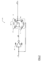
- Figure 3 shows a level shifter according to an embodiment of the invention; and
- Figure 4 shows a level shifter according to a further embodiment of the invention.
- Referring to Figure 1, a
flash memory device 100 is schematically represented. Thememory device 100 includes one or more sectors 105 (only one shown in the Figure). Thesector 105 includes a plurality of memory cells MC, each one consisting of a floating gate MOSFET transistor. In particular, thememory device 100 is of the flash type, wherein the memory cells MC of eachsector 105 must be erased at the same time. - In an erased condition each memory cell MC has a low threshold voltage (to which a logical level "1" is typically associated). The memory cell MC is programmed by injecting electrons into its floating-gate; in this condition the memory cell MC has a high threshold voltage (to which a logical level "0" is typically associated).
- In each
sector 105, the memory cells MC are arranged in rows and columns. The memory cells MC of each column have the drain terminals connected to a respective bit line BL, while the memory cells MC of each row have the gate terminals connected to a respective word line WL. The source terminal of each memory cell MC receives a reference voltage GND (or ground). - The
memory device 100 further includes a PMU (acronym for Power Management Unit) 110. ThePMU 110 provides the biasing voltages that are used for performing the conventional operations (such as read, program, erase and verify) on thememory device 100. ThePMU 110 receives a supply voltage Vdd (such as 3V) from the outside and outputs different operative voltages Vhv; the operative voltages Vhv are generally higher in absolute value than the supply voltage Vdd, for example, ranging from -9V to 9V. For this purpose, thePMU 110 includes a circuitry (e.g., charge pumps) adapted to generate the operative voltages Vhv from the supply voltage Vdd. Preferably, those charge pumps are implemented by means of low voltage transistors only, as described in Patent Application No.EP05111284.5 filed on 25 November 2005 - Moreover, the
memory device 100 receives an addressing code ADD for accessing the memory cells MC. The addressing code ADD consists of a logical signal formed by a set of bits (such as 8-32); each bit can be at the supply voltage Vdd (for example, logical level "1") or at the ground voltage GND (for example, logical level "0"). A portion of the addressing code ADD is supplied to acolumn decoder 120, which selects a set of desired bit lines BL (such as 8). Another portion of the addressing code ADD is supplied to arow decoder 125, which selects one desired word line WL. - The
column decoder 120 couples the selected bit lines BL to a read-write circuit 130. The read/write circuit 130 includes all the components (e.g., sense amplifiers, comparators, reference current/voltage generators, pulse generators, program load circuits and the like), which are normally required for writing the desired logical values into the selected memory cells MC and for reading the logical values currently stored therein. The read/write circuit 130 is coupled to externally-accessible terminals of the memory device 100 (not shown in figure) for receiving/delivering data. - The
row decoder 125 includes aselector 130, which receives the corresponding portion of the addressing code ADD and provides a (logical) selection signal Vp for each word line WL; for example, the selection signal Vp of the selected word line WL is asserted (at the logical value 1) whereas the other selection signals Vp are deasserted (at the logical value 0). Each selection signal Vp is provided to a correspondinglevel shifter 135. Thelevel shifter 135 converts the logical value of the selection signal Vp (GND-Vdd) to one of the operative voltages Vhv (from -9V to 9V, according to the operations to be performed on the memory device 100). - Referring to Figure 2, a schematic representation of a
generic level shifter 135 known in the art is shown. Thelevel shifter 135 includes aninverter 203, for example of CMOS type, and a shifter circuit 205. Theinverter 203 is supplied between the voltages Vdd and GND. Theinverter 203 receives the selection signal Vp from the selector (not shown in the figure) and provides a corresponding complemented selection signal Vp# to the shifter circuit 205. The shifter circuit 205 has a latch structure that includes two p-channel MOSFET transistors P1 and P2 and two n-channel MOSFET transistors N1 and N2. The transistors P1 and P2 have the source terminals that receive one of the operative voltages Vhv, such as a program voltage POSV (for example, POSV = 9V). The transistors N1 and N2 have the corresponding drain terminals that are connected to the drain terminals of the transistors P1 and P2, respectively. The gate terminal of the transistor P1 is connected to the drain terminal of the transistor P2, which provides an output signal OUT to the corresponding word line (not shown in the figure); the gate terminal of the transistor P2 is connected to the drain terminal of the transistor P1. - The transistors N1 and N2 have the source terminals that receive the reference voltage GND. The gate terminal of the transistor N2 directly receives the selection signal Vp. The transistor N1 has the gate terminal that receives the complemented selection signal Vp# from the
inverter 203. - When the selection signal Vp is asserted (at the supply voltage Vdd) the complemented selection signal Vp# is deasserted (at the reference voltage GND). In this biasing condition, the transistor N2 is on. Therefore, the output signal OUT is brought to the reference voltage GND.
- At the same time, the transistor N1 is off. As a result, the transistor P1 is on (because its gate terminal receives the reference voltage GND by means of the transistor N2). However, the transistor P1 is connected in series to the transistor N1, thus both the transistors N1 and P1 cannot conduct any current because the transistor N1 is off. The transistor P1 has the drain terminal that is brought to the program voltage POSV. In this biasing condition, the transistor P2 is also off, so as not to interfere with the output signal OUT.
- On the contrary, when the selection signal Vp is deasserted and the complemented selection signal Vp# is asserted, the transistor N1 is on and the transistor N2 is off. In this way, the transistor P2 is turned on and the transistor P1 is turned off, so as to bring the output signal OUT to the program voltage POSV.
- In the
level shifter 135 the driving voltage of the transistors N1 and N2 (between the gate and source/drain terminals) may reach the program voltage POSV = 9V, when are driven (at the gate terminals) by the reference voltage GND and receive the program voltage POSV at the drain terminals (through the transistors P2 and P1, respectively). Likewise, the driving voltage of the transistors P1 and P2 may reach the program voltage POSV = 9V, when they are driven by the reference voltage GND (through the transistors N1 and N2, respectively). Thus, the driving voltage of the transistors N1, N2, P1 and P2 is higher than the supply voltage Vdd. The transistors P1, P2, N1 and N2 must then be designed in such a way to guarantee the capability of sustaining, between their gate terminal and any other terminal thereof, voltage differences up to the program voltage POSV. - For this purpose, the transistors P1, P2, N1 and N2 have a thick gate oxide layer. In other words, the transistors P1, P2, N1 and N2 must be high voltage transistors (with the drawbacks discussed in the foregoing).
- Referring now to Figure 3, a level shifter according to an embodiment of the present invention is schematically shown (this implementation is differentiated by adding an apex to its reference, i.e., 135').
- In particular, the level shifter 135' includes an
input circuit 305 that is coupled to aninterface circuit 310. Theinterface circuit 310 is in turn coupled to anoutput circuit 315. - More in detail, the
input circuit 305 includes two p-channel MOSFET transistors M1 and M2 and aninverter 320, which is supplied between the voltages Vdd and GND. As above, theinverter 320 receives the selection signal Vp and provides the complemented selection signal Vp#. - The gate terminal of the transistor M2 receives the selection signal Vp and the gate terminal of the transistor M1 receives the complemented selection signal Vp# (through the inverter 320). The drain terminal of the transistor M2 is connected to the gate terminal of the transistor M1, and the gate terminal of the transistor M2 is connected to the drain terminal of the transistor M1.
- The source terminals of the transistors M1 and M2 (denoted as intermediate nodes IN1 and IN2, respectively) are connected to the
interface circuit 310. In particular, theinterface circuit 310 includes two n-channel MOSFET transistors M3 and M4. The transistors M3 and M4 have the source terminals connected to the intermediate nodes IN1 and IN2, respectively, and the drain terminals that are connected to the output circuit 315 (denoted as output nodes OUT1 and OUT2, respectively). Moreover, the gate terminals of the transistors M3 and M4 are connected together and receive a predetermined gate voltage VG1. The gate voltage VG1 is higher than the supply voltage Vdd; more specifically, the gate voltage VG1 is equal at least to the supply voltage Vdd plus a typical threshold voltage of the transistors M3 and M4, such as VG1 = 3V + 1V = 4V. For example, the gate voltage VG1 is provided by means of a voltage regulator which is included in the PMU of the memory device. - The
output circuit 315 has a latch structure as in Figure 2, which is implemented by two p-channel MOSFET transistors M5 and M6 (with the node OUT2 that provides a different output signal OUT'). In this case, the source terminals of the transistors M5 and M6 receive one of the operative voltages Vhv (denoted with POSV1), which is equal at most to twice the supply voltage Vdd (for example, POSV1 = 6V). - In other words, the level shifter 135' has a first and a second circuital branches, wherein the first branch includes the transistors M1, M3, M5 (connected in series) and the second branch includes the transistors M2, M4 and M6 (connected in series).
- During operation of the level shifter 135', when the selection signal Vp is asserted (at the supply voltage Vdd), the complemented selection signal Vp# is deasserted (at the reference voltage GND). In this biasing condition, the transistor M1 is on. Thus, the transistor M1 brings the intermediate node IN1 to the supply voltage Vdd. The transistor M3 is turned on as well. In this way, the voltage of the output node OUT1 reaches the supply voltage Vdd. As a result, the transistor M6 is turned on and the output node OUT2 is brought to the operative voltage POSV1.
- In this biasing condition, the transistor M5 is off (because its driving voltage is equal to zero), so that the output node OUT1 remains at the supply voltage Vdd. Since the transistor M2 is off, the transistor M4 cannot conduct any current as well.
- On the contrary, when the selection signal Vp is deasserted (at the reference voltage GND), the transistors M2, M4 and M5 are turned on and the transistors M1, M3 and M6 are turned off, so as to bring the output node OUT2 to the supply voltage Vdd (with the output node OUT1 that is at the operative voltage POSV1).
- As can be noted, during the operation of the level shifter 135', each transistor M1 - M6 sustains (between its gate terminal and any other terminal thereof) voltage differences at most equal to the supply voltage Vdd.
- Particularly, thanks to the
interface circuit 310, when the transistors M5 and M6 are on they are driven by the supply voltage Vdd (and not by the reference voltage GND as in the preceding case); therefore, their driving voltage remains equal to POSV1-Vdd and then at most equal to Vdd (being POSV1 ≤ 2Vdd). Likewise, when the transistors M1 and M2 are off they receive the supply voltage Vdd at the drain terminals through the transistors M3 and M4, respectively (instead of the operative voltage POSV1). - In such a way, the level shifter 135' can be implemented with low voltage transistors only.
- Therefore, it is possible to avoid the use of high voltage transistors having thick oxide layers (capable to sustain voltages higher than the supply voltage Vdd). This reduces the area occupied by the memory device in a chip of semiconductor material where it is integrated.
- Moreover, the number of processing steps and masks are reduced significantly: this has a beneficial impact on the whole manufacturing process of the memory device.
- However, in the level shifter 135', if the operative voltages were higher than 2Vdd, the transistors M5 and M6 would experience driving voltages higher than the supply voltage Vdd (so that they could not be implemented with low voltage transistors).
- In order to overcome this limitation, a level shifter according to a further embodiment of the present invention is proposed in Figure 4 (this implementation is differentiated by adding a double apex to its reference, i.e., 135").
- In particular, the
level shifter 135" includes the level shifter 135' described above and a further (simplified) level shifter (which is differentiated by adding the index 's' to its references). Thesimplified level shifter 135's has a circuital structure as the one of level shifter 135' except for the lack of theinverter 320. The level shifter 135' and thelevel shifter 135's are cascade connected. More in particular, the gate terminal of the transistor M1s is coupled to the output node OUT1 and the gate terminal of the transistor M2s is coupled to the output node OUT2. - Moreover, all the voltages applied to the transistors M1s - M6s are increased by the supply voltage Vdd. In detail, the transistors M1s and M2s are now driven alternatively by the supply voltage Vdd or the operative voltage POSV1 (provided by the level shifter 135'). Moreover, the transistors M3s and M4s receive a gate voltage VG2 that is equal to the operative voltage POSV1 plus their threshold voltage, such as VG2 = 6V + 1V = 7V. Likewise, the source terminals of the transistors M5s and M6s receive one of the operative voltages Vhv (denoted with POSV2), which is equal at most to three times the supply voltage Vdd (for example, POSV2 = 9V).
- In this case, the output node OUT2s provides a higher output signal OUT" to the corresponding word line (not shown in the figure).
- As described above, when the selection signal Vp is asserted (at the supply voltage Vdd), the output node OUT1 is at the supply voltage Vdd whereas the output node OUT2 is at the operative voltage POSV1. The operation of the level shifter 135s' is exactly the same of the level shifter 135', with the only difference that its voltages are shifted by the supply voltage Vdd. Particularly, in this biasing condition the transistor M1s is on, so bringing the intermediate node IN1s to the operative voltage POSV1. The transistor M3s is turned on as well. In this way, the voltage of the output node OUT1s reaches the operative voltage POSV1. As a result, the transistor M6s is turned on and the output node OUT2s is brought to the operative voltage POSV2.
- In this biasing condition, the transistor M5s is off (because its driving voltage is equal to zero), so that the output node OUT1s remains at the operative voltage POSV1. Since the transistor M2s is off, the transistor M4s cannot conduct any current as well.
- On the contrary, when the selection signal Vp is deasserted (at the reference voltage GND), the transistors M2s, M4s and M5s are turned on and the transistors M1s, M3s and M6s are turned off, so as to bring the output node OUT2s (and thus the output signal OUT") to the operative voltage POSV1 (with the output node OUT1s that is at the operative voltage POSV2).
- As can be noted, during the operation of the
level shifter 135", each transistor M1s - M6s sustains (between its gate terminal and any other terminal thereof) voltage differences at most equal to the supply voltage Vdd. - Particularly, when the transistors M5s and M6s are on they are driven by the operative voltage POSV1; therefore, their driving voltage remains equal to POSV2-POSV1 and then at most equal to Vdd (being POSV1 = 2Vdd and POSV2 = 3Vdd). Likewise, when the transistors M1s and M2s are off they receive the supply voltage Vdd at their gate terminals and the operative voltage POSV1 at their drain terminals (which difference is again at most equal to Vdd).
- Therefore, it is now possible to shift the selection signal Vp (GND-Vdd) to a higher output signal OUT" (POSV1 - POSV2) again using low voltage transistors only. The same structure proposed above can be replicated by adding further stages, so as to work with operative voltages up to 4Vdd with 3 stages, 5Vdd with 4 stages, and so on.
- Naturally, in order to satisfy local and specific requirements, a person skilled in the art may apply to the solution described above many modifications and alterations. Particularly, although the present invention has been described with a certain degree of particularity with reference to preferred embodiments thereof, it should be understood that various omissions, substitutions and changes in the form and details as well as other embodiments are possible; moreover, it is expressly intended that specific elements and/or method steps described in connection with any disclosed embodiment of the invention may be incorporated in any other embodiment as a general matter of design choice.
- For example, similar considerations apply if the level shifter has a similar structure even implemented with equivalent components. Moreover, it should be apparent that the numerical examples of the different voltages described above are merely illustrative and must not to be interpreted in a limitative manner.
- Likewise, the input circuit, interface circuit and/or output circuit my have alternative schemes; for example, it is possible to implement the interface circuit with two o more transistors connected in series.
- In any case, the use of other types of transistors (for example, bipolar junction transistors) is within the scope of the invention.
- Moreover, the use of MOSFET transistor having a type of conductivity opposed to that of the transistors shown in the preceding description is contemplated (so as to work with negative voltages).
- Similar considerations apply if the memory device has a different structure or includes equivalent components.
- Likewise, it is possible to use the proposed solution for biasing the selected word lines during further operations performed on the memory device.
- It should be noted that although in the preceding description large reference has been made to the row decoder, this is not to be intended as a limitation; indeed, the same techniques can also be used for implementing a column decoder adapted for biasing the selected bit lines.
Claims (10)
- A level shifter (135') including a stage having a first branch (M1, M3, M5) and a second branch (M2, M4, M6), each branch including:- a selection terminal for receiving a selection signal (Vp), the selection signal received by the first branch and the second branch being alternatively at a first voltage (GND) and at a second voltage (Vdd) higher than the first voltage in absolute value,- a service terminal for receiving a third voltage (POSV1) higher than the second voltage in absolute value,- an input circuit (305) for coupling an intermediate node (IN1, IN2) to the selection terminal when at the second voltage or for insulating the intermediate node from the selection terminal otherwise,- an interface circuit (310) for coupling an output terminal (OUT1, OUT2) to the intermediate node when coupled or for insulating the output terminal from the intermediate node otherwise, and- an output circuit (315) for insulating the service terminal from the output terminal when coupled or for coupling the service terminal to the output terminal otherwise, the output terminals of the first branch and the second branch providing an output signal being alternatively at the second voltage or at the third voltage according to the selection signal.
- The level shifter (135') according to claim 1, wherein in each branch (M1, M3, M5; M2, M4, M6) the input circuit (305) includes an input transistor (M1, M2) having a first conduction terminal coupled to the intermediate node (IN1, IN2) of the branch, a second conduction terminal coupled to the selection terminal of the branch, and a control terminal coupled to the selection terminal of the other branch.
- The level shifter (135') according to claim 1 or 2, wherein in each branch (M1, M3, M5; M2, M4, M6) the interface circuit (310) includes an interface transistor (M3, M4) having a first conduction terminal coupled to the intermediate node (IN1, IN2), a second conduction terminal coupled to the output terminal (OUT1, OUT2), and a control terminal for receiving a biasing voltage comprised between the second voltage and the third voltage.
- The level shifter (135') according to claim 3, wherein the interface transistor (M3, M4) has a predefined threshold voltage, the biasing voltage being at least equal to the second voltage plus the threshold voltage.
- The level shifter (135') according to any claim from 1 to 4, wherein in each branch (M1, M3, M5; M2, M4, M6) the output circuit (315) includes an output transistor (M5, M6) having a first conduction terminal coupled to the service terminal of the branch, a second conduction terminal coupled to the output terminal (OUT1, OUT2) of the branch, and a control terminal coupled to the output terminal of the other branch.
- The level shifter (135") according to any one of the preceding claim, wherein the level shifter includes at least one further stage (135's), all the stages (135', 135's) being cascade connected in a sequence, and wherein for each next stage different from a first stage in the sequence each selection terminal is coupled to the corresponding output terminal of a preceding stage in the sequence.
- The level shifter (135') according to any claim from 1 to 6, wherein for each stage the difference between the second voltage and the first voltage and the difference between the third voltage and the second voltage is at most equal to a power supply voltage, each transistor (M1 - M6) being a low-voltage transistor adapted to sustain at most the power supply voltage between each pair of terminals thereof.
- The level shifter (135') according to claim 7, wherein each transistor (M1 - M6) is a MOSFET transistor, the input transistors (M1, M2) and the output transistors (M5, M6) having a first type of conductivity and the interface transistors (M3, M4) having a second type of conductivity, the second type of conductivity being opposite to the first type of conductivity.
- A memory device (100) including a plurality of memory cells (MC) arranged in at least one plurality of alignments, for each plurality of alignments the memory device including means (130) for providing a selection signal (Vp) for each alignment in response to an address code (ADD), and the level shifter (135') according to any claim from 1 to 8 for each alignment for receiving the corresponding selection signal and for applying the output signal to the corresponding alignment.
- A level shifting method implemented by a level shifter (135') including a stage having a first branch (M1, M3, M5) and a second branch (M2, M4, M6), the method including the steps of:- receiving a selection signal (Vp) at a selection terminal, the selection signal received by the first branch and the second branch being alternatively at a first voltage (GND) and at a second voltage (Vdd) higher than the first voltage in absolute value,- receiving a third voltage (POSV1) at a service terminal higher than the second voltage in absolute value,- coupling an intermediate node (IN1, IN2) to the selection terminal when at the second voltage or insulating the intermediate node from the selection terminal otherwise,- coupling an output terminal (OUT1, OUT2) to the intermediate node when coupled or insulating the output terminal from the intermediate node otherwise, and- insulating the service terminal from the output terminal when coupled or coupling the service terminal to the output terminal otherwise, the output terminals of the first branch and the second branch providing an output signal being alternatively at the second voltage or at the third voltage according to the selection signal.
Priority Applications (6)
| Application Number | Priority Date | Filing Date | Title |
|---|---|---|---|
| EP06111337A EP1835507B1 (en) | 2006-03-17 | 2006-03-17 | Level shifter for semiconductor memory device implemented with low-voltage transistors |
| DE602006016230T DE602006016230D1 (en) | 2006-03-17 | 2006-03-17 | A level shifter implemented for low voltage transistors for a semiconductor memory device |
| US11/605,209 US7499345B2 (en) | 2005-11-25 | 2006-11-27 | Non-volatile memory implemented with low-voltages transistors and related system and method |
| US11/605,193 US20070170979A1 (en) | 2005-11-25 | 2006-11-27 | Charge pump systems and methods |
| CN200710088621XA CN101038790B (en) | 2006-03-17 | 2007-03-16 | Level shifter for semiconductor memory device implemented with low-voltage transistors |
| US11/725,988 US7592849B2 (en) | 2006-03-17 | 2007-03-19 | Level shifter for semiconductor memory device implemented with low-voltage transistors |
Applications Claiming Priority (1)
| Application Number | Priority Date | Filing Date | Title |
|---|---|---|---|
| EP06111337A EP1835507B1 (en) | 2006-03-17 | 2006-03-17 | Level shifter for semiconductor memory device implemented with low-voltage transistors |
Publications (2)
| Publication Number | Publication Date |
|---|---|
| EP1835507A1 true EP1835507A1 (en) | 2007-09-19 |
| EP1835507B1 EP1835507B1 (en) | 2010-08-18 |
Family
ID=36794958
Family Applications (1)
| Application Number | Title | Priority Date | Filing Date |
|---|---|---|---|
| EP06111337A Expired - Lifetime EP1835507B1 (en) | 2005-11-25 | 2006-03-17 | Level shifter for semiconductor memory device implemented with low-voltage transistors |
Country Status (4)
| Country | Link |
|---|---|
| US (1) | US7592849B2 (en) |
| EP (1) | EP1835507B1 (en) |
| CN (1) | CN101038790B (en) |
| DE (1) | DE602006016230D1 (en) |
Cited By (2)
| Publication number | Priority date | Publication date | Assignee | Title |
|---|---|---|---|---|
| US7592849B2 (en) | 2006-03-17 | 2009-09-22 | Stmicroelectronics, S.R.L. | Level shifter for semiconductor memory device implemented with low-voltage transistors |
| WO2019173272A1 (en) * | 2018-03-05 | 2019-09-12 | Texas Instruments Incorporated | Level shifter circuit |
Families Citing this family (14)
| Publication number | Priority date | Publication date | Assignee | Title |
|---|---|---|---|---|
| US7772912B2 (en) * | 2007-11-13 | 2010-08-10 | Himax Technologies Limited | Level shift circuit and method thereof |
| US7859919B2 (en) * | 2008-08-27 | 2010-12-28 | Freescale Semiconductor, Inc. | Memory device and method thereof |
| US7804350B1 (en) | 2009-04-22 | 2010-09-28 | Semiconductor Components Industries, Llc | Level shifting using cross-coupled cascode transistors |
| JP5870368B2 (en) * | 2010-02-12 | 2016-03-01 | スペロ・デバイシーズ・インコーポレーテッド | Components that process wideband analog radio frequencies |
| TWI410048B (en) * | 2010-06-03 | 2013-09-21 | Orise Technology Co Ltd | Level shifter |
| JP6030334B2 (en) * | 2011-05-20 | 2016-11-24 | 株式会社半導体エネルギー研究所 | Storage device |
| CN104318957B (en) * | 2014-10-24 | 2017-07-18 | 中国人民解放军国防科学技术大学 | A kind of level translator |
| US9553584B2 (en) * | 2014-12-23 | 2017-01-24 | International Business Machines Corporation | Level-shifting latch |
| CN105761743B (en) * | 2016-01-29 | 2018-05-25 | 上海华虹宏力半导体制造有限公司 | Line decoder and memory |
| CN105741867B (en) * | 2016-01-29 | 2018-05-08 | 上海华虹宏力半导体制造有限公司 | Line decoder and memory |
| TWI681628B (en) * | 2018-06-11 | 2020-01-01 | 瑞昱半導體股份有限公司 | Voltage level shifter circuit |
| TWI707541B (en) * | 2020-04-17 | 2020-10-11 | 瑞昱半導體股份有限公司 | Voltage level conversion circuit |
| KR102789800B1 (en) * | 2020-09-16 | 2025-04-01 | 삼성전자주식회사 | Negative level shifter and nonvolatile memory device including the same |
| US20260045950A1 (en) * | 2024-08-12 | 2026-02-12 | Stmicroelectronics International N.V. | Level shifting circuit |
Citations (7)
| Publication number | Priority date | Publication date | Assignee | Title |
|---|---|---|---|---|
| US4318015A (en) * | 1979-06-29 | 1982-03-02 | Rca Corporation | Level shift circuit |
| EP0608489A2 (en) * | 1993-01-28 | 1994-08-03 | United Memories, Inc. | Low-to-high voltage translator with latch-up immunity |
| US6111425A (en) * | 1998-10-15 | 2000-08-29 | International Business Machines Corporation | Very low power logic circuit family with enhanced noise immunity |
| US6351173B1 (en) * | 2000-08-25 | 2002-02-26 | Texas Instruments Incorporated | Circuit and method for an integrated level shifting latch |
| US20020030204A1 (en) * | 2000-06-09 | 2002-03-14 | Yasuaki Hirano | Voltage level shifter circuit and nonvolatile semiconductor storage device using the circuit |
| US20030011418A1 (en) * | 2001-07-16 | 2003-01-16 | Matsushita Electric Industrial Co., Ltd. | Level shifting circuit |
| EP1791245A1 (en) | 2005-11-25 | 2007-05-30 | STMicroelectronics S.r.l. | Charge pump circuit |
Family Cites Families (43)
| Publication number | Priority date | Publication date | Assignee | Title |
|---|---|---|---|---|
| JPS5654693A (en) * | 1979-10-05 | 1981-05-14 | Hitachi Ltd | Programable rom |
| FR2607338A1 (en) * | 1986-11-21 | 1988-05-27 | Eurotechnique Sa | VOLTAGE SWITCHING CIRCUIT IN MOS TECHNOLOGY |
| US5223451A (en) * | 1989-10-06 | 1993-06-29 | Kabushiki Kaisha Toshiba | Semiconductor device wherein n-channel MOSFET, p-channel MOSFET and nonvolatile memory cell are formed in one chip and method of making it |
| US5287536A (en) * | 1990-04-23 | 1994-02-15 | Texas Instruments Incorporated | Nonvolatile memory array wordline driver circuit with voltage translator circuit |
| DE69229995T2 (en) | 1992-06-30 | 2000-03-16 | Stmicroelectronics S.R.L. | Voltage regulator for storage devices |
| JPH06324753A (en) * | 1993-05-13 | 1994-11-25 | Fujitsu Ltd | Constant voltage generating circuit and semiconductor memory |
| US5475335A (en) * | 1994-04-01 | 1995-12-12 | National Semiconductor Corporation | High voltage cascaded charge pump |
| US6475846B1 (en) * | 1995-05-18 | 2002-11-05 | Texas Instruments Incorporated | Method of making floating-gate memory-cell array with digital logic transistors |
| US5631606A (en) | 1995-08-01 | 1997-05-20 | Information Storage Devices, Inc. | Fully differential output CMOS power amplifier |
| US5748025A (en) * | 1996-03-29 | 1998-05-05 | Intel Corporation | Method and apparatus for providing high voltage with a low voltage CMOS integrated circuit |
| US5736869A (en) * | 1996-05-16 | 1998-04-07 | Lsi Logic Corporation | Output driver with level shifting and voltage protection |
| US6487687B1 (en) * | 1997-01-02 | 2002-11-26 | Texas Instruments Incorporated | Voltage level shifter with testable cascode devices |
| US5796656A (en) * | 1997-02-22 | 1998-08-18 | Programmable Microelectronics Corporation | Row decoder circuit for PMOS non-volatile memory cell which uses electron tunneling for programming and erasing |
| US6023085A (en) * | 1997-12-18 | 2000-02-08 | Advanced Micro Devices, Inc. | Core cell structure and corresponding process for NAND-type high performance flash memory device |
| US6002290A (en) * | 1997-12-23 | 1999-12-14 | Sarnoff Corporation | Crisscross voltage level shifter |
| JP3389856B2 (en) * | 1998-03-24 | 2003-03-24 | 日本電気株式会社 | Semiconductor device |
| EP1005079B1 (en) * | 1998-11-26 | 2012-12-26 | STMicroelectronics Srl | Process for integrating in a same chip a non-volatile memory and a high-performance logic circuitry |
| IT1313227B1 (en) * | 1999-07-02 | 2002-06-17 | St Microelectronics Srl | VOLTAGE TRANSLATOR, IN PARTICULAR CMOS TYPE. |
| US6407579B1 (en) * | 2000-01-20 | 2002-06-18 | Koninklijke Philips Electronics N.V. | Fast high voltage level shifter with gate oxide protection |
| JP4057756B2 (en) * | 2000-03-01 | 2008-03-05 | 松下電器産業株式会社 | Semiconductor integrated circuit |
| IT1316872B1 (en) * | 2000-03-31 | 2003-05-12 | St Microelectronics Srl | PARTICULAR VOLTAGE TRANSLATOR OF CMOS TYPE |
| US6370071B1 (en) * | 2000-09-13 | 2002-04-09 | Lattice Semiconductor Corporation | High voltage CMOS switch |
| JP2002118177A (en) * | 2000-10-11 | 2002-04-19 | Toshiba Corp | Semiconductor device and manufacturing method thereof |
| FR2816751A1 (en) * | 2000-11-15 | 2002-05-17 | St Microelectronics Sa | Flash memory erasable by page and method for data storaage, comprising array with counter and sectors, and circuits for reading page address and incrementing counter |
| FR2817413B1 (en) * | 2000-11-29 | 2003-02-28 | St Microelectronics Sa | HIGH VOLTAGE SWITCHING DEVICE AND APPLICATION TO A NON-VOLATILE MEMORY |
| FR2822309B1 (en) * | 2001-03-19 | 2003-06-13 | St Microelectronics Sa | SWITCHING SIGNAL TRANSLATION CIRCUIT |
| KR100407573B1 (en) * | 2001-08-09 | 2003-11-28 | 삼성전자주식회사 | Method of forming non volatile memory having floating trap type device |
| JP3851791B2 (en) * | 2001-09-04 | 2006-11-29 | 株式会社東芝 | Semiconductor integrated circuit |
| JP3906177B2 (en) * | 2002-05-10 | 2007-04-18 | 株式会社東芝 | Nonvolatile semiconductor memory device |
| US6741115B2 (en) * | 2002-06-18 | 2004-05-25 | Ip-First, Llc | Digital level shifter for maintaining gate oxide integrity of scaled driver devices |
| JP2004349377A (en) * | 2003-05-21 | 2004-12-09 | Sharp Corp | Semiconductor device and its manufacturing method |
| US7053657B1 (en) * | 2003-06-26 | 2006-05-30 | Cypress Semiconductor Corporation | Dynamically biased wide swing level shifting circuit for high speed voltage protection input/outputs |
| US7053658B1 (en) * | 2003-11-26 | 2006-05-30 | National Semiconductor Corporation | Apparatus for circuit with keeper |
| US7075140B2 (en) * | 2003-11-26 | 2006-07-11 | Gregorio Spadea | Low voltage EEPROM memory arrays |
| KR100521385B1 (en) * | 2003-12-15 | 2005-10-12 | 삼성전자주식회사 | High voltage generator circuit and semiconductor memory device including the same |
| DE102004004271A1 (en) * | 2004-01-28 | 2005-08-18 | Texas Instruments Deutschland Gmbh | High speed level shifter with AC feedforward |
| US7151391B2 (en) * | 2004-05-24 | 2006-12-19 | Taiwan Semiconductor Manufacturing Company, Ltd. | Integrated circuit for level-shifting voltage levels |
| US7215146B2 (en) * | 2004-10-29 | 2007-05-08 | Intel Corporation | High speed buffered level-up shifters |
| US7183817B2 (en) * | 2005-06-29 | 2007-02-27 | Freescale Semiconductor, Inc. | High speed output buffer with AC-coupled level shift and DC level detection and correction |
| EP1892600B1 (en) | 2006-08-24 | 2016-07-27 | Micron Technology, Inc. | Voltage regulator for non-volatile memories implemented with low-voltage transistors |
| EP1837993B1 (en) | 2006-03-21 | 2010-01-27 | STMicroelectronics S.r.l. | Improvements to the design of voltage switches |
| EP1835507B1 (en) | 2006-03-17 | 2010-08-18 | STMicroelectronics Srl | Level shifter for semiconductor memory device implemented with low-voltage transistors |
| JP5065594B2 (en) * | 2005-12-23 | 2012-11-07 | 株式会社東芝 | Semiconductor memory device |
-
2006
- 2006-03-17 EP EP06111337A patent/EP1835507B1/en not_active Expired - Lifetime
- 2006-03-17 DE DE602006016230T patent/DE602006016230D1/en not_active Expired - Lifetime
-
2007
- 2007-03-16 CN CN200710088621XA patent/CN101038790B/en active Active
- 2007-03-19 US US11/725,988 patent/US7592849B2/en active Active
Patent Citations (7)
| Publication number | Priority date | Publication date | Assignee | Title |
|---|---|---|---|---|
| US4318015A (en) * | 1979-06-29 | 1982-03-02 | Rca Corporation | Level shift circuit |
| EP0608489A2 (en) * | 1993-01-28 | 1994-08-03 | United Memories, Inc. | Low-to-high voltage translator with latch-up immunity |
| US6111425A (en) * | 1998-10-15 | 2000-08-29 | International Business Machines Corporation | Very low power logic circuit family with enhanced noise immunity |
| US20020030204A1 (en) * | 2000-06-09 | 2002-03-14 | Yasuaki Hirano | Voltage level shifter circuit and nonvolatile semiconductor storage device using the circuit |
| US6351173B1 (en) * | 2000-08-25 | 2002-02-26 | Texas Instruments Incorporated | Circuit and method for an integrated level shifting latch |
| US20030011418A1 (en) * | 2001-07-16 | 2003-01-16 | Matsushita Electric Industrial Co., Ltd. | Level shifting circuit |
| EP1791245A1 (en) | 2005-11-25 | 2007-05-30 | STMicroelectronics S.r.l. | Charge pump circuit |
Cited By (3)
| Publication number | Priority date | Publication date | Assignee | Title |
|---|---|---|---|---|
| US7592849B2 (en) | 2006-03-17 | 2009-09-22 | Stmicroelectronics, S.R.L. | Level shifter for semiconductor memory device implemented with low-voltage transistors |
| WO2019173272A1 (en) * | 2018-03-05 | 2019-09-12 | Texas Instruments Incorporated | Level shifter circuit |
| US10498315B2 (en) | 2018-03-05 | 2019-12-03 | Texas Instruments Incorporated | Level shifter circuit |
Also Published As
| Publication number | Publication date |
|---|---|
| CN101038790B (en) | 2011-11-09 |
| DE602006016230D1 (en) | 2010-09-30 |
| CN101038790A (en) | 2007-09-19 |
| EP1835507B1 (en) | 2010-08-18 |
| US7592849B2 (en) | 2009-09-22 |
| US20070241804A1 (en) | 2007-10-18 |
Similar Documents
| Publication | Publication Date | Title |
|---|---|---|
| US7592849B2 (en) | Level shifter for semiconductor memory device implemented with low-voltage transistors | |
| US6603702B2 (en) | Semiconductor integrated circuit | |
| EP0606650B1 (en) | Nonvolatile semiconductor memory device | |
| US20090180333A1 (en) | Semiconductor memory column decoder device and method | |
| JP4703162B2 (en) | Nonvolatile semiconductor memory device and writing method thereof | |
| JP2002197876A (en) | Writing method for nonvolatile storage device | |
| JP2007317247A (en) | Nonvolatile semiconductor memory device and operating method of nonvolatile semiconductor memory device | |
| US6927999B2 (en) | Integrated circuit memory devices and methods of programming the same in which the current drawn during a programming operation is independent of the data to be programmed | |
| US8270222B2 (en) | Local word line driver of a memory | |
| US8189392B2 (en) | Page buffer circuit | |
| US8638618B2 (en) | Decoder for NAND memory | |
| US7023738B2 (en) | Full-swing wordline driving circuit | |
| US20070230252A1 (en) | Row selector for a semiconductor memory device | |
| US7499345B2 (en) | Non-volatile memory implemented with low-voltages transistors and related system and method | |
| US8300460B2 (en) | Nonvolatile memory device | |
| US7965561B2 (en) | Row selector occupying a reduced device area for semiconductor memory devices | |
| US8873312B2 (en) | Decoder circuit of semiconductor storage device | |
| US20160099033A1 (en) | Column decoder circuitry for a non-volatile memory | |
| US20070285989A1 (en) | Column decoding system for semiconductor memory devices implemented with low voltage transistors | |
| CN104123963B (en) | A kind of level translator realized with low voltage transistor | |
| US6646468B2 (en) | Switching device with high-voltage translator | |
| JP2003016792A (en) | Nonvolatile semiconductor memory device | |
| US20080089125A1 (en) | Memory device | |
| US20120230117A1 (en) | Nonvolatile semicondcutor memory device | |
| US20070007561A1 (en) | Discharge circuit for a word-erasable flash memory device |
Legal Events
| Date | Code | Title | Description |
|---|---|---|---|
| PUAI | Public reference made under article 153(3) epc to a published international application that has entered the european phase |
Free format text: ORIGINAL CODE: 0009012 |
|
| AK | Designated contracting states |
Kind code of ref document: A1 Designated state(s): AT BE BG CH CY CZ DE DK EE ES FI FR GB GR HU IE IS IT LI LT LU LV MC NL PL PT RO SE SI SK TR |
|
| AX | Request for extension of the european patent |
Extension state: AL BA HR MK YU |
|
| 17P | Request for examination filed |
Effective date: 20080318 |
|
| 17Q | First examination report despatched |
Effective date: 20080422 |
|
| AKX | Designation fees paid |
Designated state(s): DE FR GB IT |
|
| R17C | First examination report despatched (corrected) |
Effective date: 20080418 |
|
| GRAP | Despatch of communication of intention to grant a patent |
Free format text: ORIGINAL CODE: EPIDOSNIGR1 |
|
| RAP1 | Party data changed (applicant data changed or rights of an application transferred) |
Owner name: STMICROELECTRONICS SRL |
|
| GRAS | Grant fee paid |
Free format text: ORIGINAL CODE: EPIDOSNIGR3 |
|
| GRAA | (expected) grant |
Free format text: ORIGINAL CODE: 0009210 |
|
| AK | Designated contracting states |
Kind code of ref document: B1 Designated state(s): DE FR GB IT |
|
| REG | Reference to a national code |
Ref country code: GB Ref legal event code: FG4D |
|
| REF | Corresponds to: |
Ref document number: 602006016230 Country of ref document: DE Date of ref document: 20100930 Kind code of ref document: P |
|
| PG25 | Lapsed in a contracting state [announced via postgrant information from national office to epo] |
Ref country code: IT Free format text: LAPSE BECAUSE OF FAILURE TO SUBMIT A TRANSLATION OF THE DESCRIPTION OR TO PAY THE FEE WITHIN THE PRESCRIBED TIME-LIMIT Effective date: 20100818 |
|
| PLBE | No opposition filed within time limit |
Free format text: ORIGINAL CODE: 0009261 |
|
| STAA | Information on the status of an ep patent application or granted ep patent |
Free format text: STATUS: NO OPPOSITION FILED WITHIN TIME LIMIT |
|
| 26N | No opposition filed |
Effective date: 20110519 |
|
| PGFP | Annual fee paid to national office [announced via postgrant information from national office to epo] |
Ref country code: GB Payment date: 20110224 Year of fee payment: 6 |
|
| REG | Reference to a national code |
Ref country code: DE Ref legal event code: R097 Ref document number: 602006016230 Country of ref document: DE Effective date: 20110519 |
|
| REG | Reference to a national code |
Ref country code: FR Ref legal event code: ST Effective date: 20111130 |
|
| PG25 | Lapsed in a contracting state [announced via postgrant information from national office to epo] |
Ref country code: FR Free format text: LAPSE BECAUSE OF NON-PAYMENT OF DUE FEES Effective date: 20110331 |
|
| GBPC | Gb: european patent ceased through non-payment of renewal fee |
Effective date: 20120317 |
|
| PG25 | Lapsed in a contracting state [announced via postgrant information from national office to epo] |
Ref country code: GB Free format text: LAPSE BECAUSE OF NON-PAYMENT OF DUE FEES Effective date: 20120317 |
|
| PGFP | Annual fee paid to national office [announced via postgrant information from national office to epo] |
Ref country code: DE Payment date: 20250218 Year of fee payment: 20 |
|
| REG | Reference to a national code |
Ref country code: DE Ref legal event code: R071 Ref document number: 602006016230 Country of ref document: DE |