JP5870368B2 - Components that process wideband analog radio frequencies - Google Patents
Components that process wideband analog radio frequencies Download PDFInfo
- Publication number
- JP5870368B2 JP5870368B2 JP2012553037A JP2012553037A JP5870368B2 JP 5870368 B2 JP5870368 B2 JP 5870368B2 JP 2012553037 A JP2012553037 A JP 2012553037A JP 2012553037 A JP2012553037 A JP 2012553037A JP 5870368 B2 JP5870368 B2 JP 5870368B2
- Authority
- JP
- Japan
- Prior art keywords
- integrator
- channel
- transistor
- gate
- circuit
- Prior art date
- Legal status (The legal status is an assumption and is not a legal conclusion. Google has not performed a legal analysis and makes no representation as to the accuracy of the status listed.)
- Expired - Fee Related
Links
Images


Classifications
-
- H—ELECTRICITY
- H03—ELECTRONIC CIRCUITRY
- H03F—AMPLIFIERS
- H03F3/00—Amplifiers with only discharge tubes or only semiconductor devices as amplifying elements
- H03F3/45—Differential amplifiers
-
- H—ELECTRICITY
- H03—ELECTRONIC CIRCUITRY
- H03F—AMPLIFIERS
- H03F3/00—Amplifiers with only discharge tubes or only semiconductor devices as amplifying elements
- H03F3/45—Differential amplifiers
- H03F3/45071—Differential amplifiers with semiconductor devices only
- H03F3/45076—Differential amplifiers with semiconductor devices only characterised by the way of implementation of the active amplifying circuit in the differential amplifier
- H03F3/45179—Differential amplifiers with semiconductor devices only characterised by the way of implementation of the active amplifying circuit in the differential amplifier using MOSFET transistors as the active amplifying circuit
- H03F3/45183—Long tailed pairs
-
- H—ELECTRICITY
- H03—ELECTRONIC CIRCUITRY
- H03F—AMPLIFIERS
- H03F1/00—Details of amplifiers with only discharge tubes, only semiconductor devices or only unspecified devices as amplifying elements
- H03F1/08—Modifications of amplifiers to reduce detrimental influences of internal impedances of amplifying elements
- H03F1/22—Modifications of amplifiers to reduce detrimental influences of internal impedances of amplifying elements by use of cascode coupling, i.e. earthed cathode or emitter stage followed by earthed grid or base stage respectively
- H03F1/223—Modifications of amplifiers to reduce detrimental influences of internal impedances of amplifying elements by use of cascode coupling, i.e. earthed cathode or emitter stage followed by earthed grid or base stage respectively with MOSFET's
-
- H—ELECTRICITY
- H03—ELECTRONIC CIRCUITRY
- H03F—AMPLIFIERS
- H03F3/00—Amplifiers with only discharge tubes or only semiconductor devices as amplifying elements
- H03F3/189—High frequency amplifiers, e.g. radio frequency amplifiers
- H03F3/19—High frequency amplifiers, e.g. radio frequency amplifiers with semiconductor devices only
-
- H—ELECTRICITY
- H03—ELECTRONIC CIRCUITRY
- H03F—AMPLIFIERS
- H03F3/00—Amplifiers with only discharge tubes or only semiconductor devices as amplifying elements
- H03F3/45—Differential amplifiers
- H03F3/45071—Differential amplifiers with semiconductor devices only
- H03F3/45076—Differential amplifiers with semiconductor devices only characterised by the way of implementation of the active amplifying circuit in the differential amplifier
- H03F3/45179—Differential amplifiers with semiconductor devices only characterised by the way of implementation of the active amplifying circuit in the differential amplifier using MOSFET transistors as the active amplifying circuit
- H03F3/45183—Long tailed pairs
- H03F3/45188—Non-folded cascode stages
-
- H—ELECTRICITY
- H03—ELECTRONIC CIRCUITRY
- H03F—AMPLIFIERS
- H03F3/00—Amplifiers with only discharge tubes or only semiconductor devices as amplifying elements
- H03F3/45—Differential amplifiers
- H03F3/45071—Differential amplifiers with semiconductor devices only
- H03F3/45076—Differential amplifiers with semiconductor devices only characterised by the way of implementation of the active amplifying circuit in the differential amplifier
- H03F3/45179—Differential amplifiers with semiconductor devices only characterised by the way of implementation of the active amplifying circuit in the differential amplifier using MOSFET transistors as the active amplifying circuit
- H03F3/45197—Pl types
- H03F3/45201—Non-folded cascode stages
-
- H—ELECTRICITY
- H03—ELECTRONIC CIRCUITRY
- H03H—IMPEDANCE NETWORKS, e.g. RESONANT CIRCUITS; RESONATORS
- H03H11/00—Networks using active elements
- H03H11/02—Multiple-port networks
- H03H11/04—Frequency selective two-port networks
-
- H—ELECTRICITY
- H03—ELECTRONIC CIRCUITRY
- H03H—IMPEDANCE NETWORKS, e.g. RESONANT CIRCUITS; RESONATORS
- H03H11/00—Networks using active elements
- H03H11/02—Multiple-port networks
- H03H11/04—Frequency selective two-port networks
- H03H11/12—Frequency selective two-port networks using amplifiers with feedback
- H03H11/1217—Frequency selective two-port networks using amplifiers with feedback using a plurality of operational amplifiers
- H03H11/1252—Two integrator-loop-filters
- H03H11/1256—Tow-Thomas biquad
-
- H—ELECTRICITY
- H03—ELECTRONIC CIRCUITRY
- H03H—IMPEDANCE NETWORKS, e.g. RESONANT CIRCUITS; RESONATORS
- H03H11/00—Networks using active elements
- H03H11/02—Multiple-port networks
- H03H11/24—Frequency-independent attenuators
-
- H—ELECTRICITY
- H03—ELECTRONIC CIRCUITRY
- H03H—IMPEDANCE NETWORKS, e.g. RESONANT CIRCUITS; RESONATORS
- H03H11/00—Networks using active elements
- H03H11/46—One-port networks
- H03H11/53—One-port networks simulating resistances; simulating resistance multipliers
-
- H—ELECTRICITY
- H03—ELECTRONIC CIRCUITRY
- H03H—IMPEDANCE NETWORKS, e.g. RESONANT CIRCUITS; RESONATORS
- H03H7/00—Multiple-port networks comprising only passive electrical elements as network components
- H03H7/48—Networks for connecting several sources or loads, working on the same frequency or frequency band, to a common load or source
- H03H7/482—Networks for connecting several sources or loads, working on the same frequency or frequency band, to a common load or source particularly adapted for use in common antenna systems
-
- H—ELECTRICITY
- H03—ELECTRONIC CIRCUITRY
- H03H—IMPEDANCE NETWORKS, e.g. RESONANT CIRCUITS; RESONATORS
- H03H7/00—Multiple-port networks comprising only passive electrical elements as network components
- H03H7/48—Networks for connecting several sources or loads, working on the same frequency or frequency band, to a common load or source
- H03H7/487—Networks for connecting several sources or loads, working on the same frequency or frequency band, to a common load or source particularly adapted as coupling circuit between transmitters and antennas
-
- H—ELECTRICITY
- H04—ELECTRIC COMMUNICATION TECHNIQUE
- H04L—TRANSMISSION OF DIGITAL INFORMATION, e.g. TELEGRAPHIC COMMUNICATION
- H04L25/00—Baseband systems
- H04L25/02—Details ; arrangements for supplying electrical power along data transmission lines
- H04L25/03—Shaping networks in transmitter or receiver, e.g. adaptive shaping networks
-
- H—ELECTRICITY
- H03—ELECTRONIC CIRCUITRY
- H03F—AMPLIFIERS
- H03F2200/00—Indexing scheme relating to amplifiers
- H03F2200/264—An operational amplifier based integrator or transistor based integrator being used in an amplifying circuit
-
- H—ELECTRICITY
- H03—ELECTRONIC CIRCUITRY
- H03F—AMPLIFIERS
- H03F2200/00—Indexing scheme relating to amplifiers
- H03F2200/36—Indexing scheme relating to amplifiers the amplifier comprising means for increasing the bandwidth
-
- H—ELECTRICITY
- H03—ELECTRONIC CIRCUITRY
- H03F—AMPLIFIERS
- H03F2203/00—Indexing scheme relating to amplifiers with only discharge tubes or only semiconductor devices as amplifying elements covered by H03F3/00
- H03F2203/45—Indexing scheme relating to differential amplifiers
- H03F2203/45318—Indexing scheme relating to differential amplifiers the AAC comprising a cross coupling circuit, e.g. two extra transistors cross coupled
-
- H—ELECTRICITY
- H03—ELECTRONIC CIRCUITRY
- H03F—AMPLIFIERS
- H03F2203/00—Indexing scheme relating to amplifiers with only discharge tubes or only semiconductor devices as amplifying elements covered by H03F3/00
- H03F2203/45—Indexing scheme relating to differential amplifiers
- H03F2203/45374—Indexing scheme relating to differential amplifiers the AAC comprising one or more discrete resistors
-
- H—ELECTRICITY
- H03—ELECTRONIC CIRCUITRY
- H03F—AMPLIFIERS
- H03F2203/00—Indexing scheme relating to amplifiers with only discharge tubes or only semiconductor devices as amplifying elements covered by H03F3/00
- H03F2203/45—Indexing scheme relating to differential amplifiers
- H03F2203/45644—Indexing scheme relating to differential amplifiers the LC comprising a cross coupling circuit, e.g. comprising two cross-coupled transistors
-
- H—ELECTRICITY
- H03—ELECTRONIC CIRCUITRY
- H03F—AMPLIFIERS
- H03F2203/00—Indexing scheme relating to amplifiers with only discharge tubes or only semiconductor devices as amplifying elements covered by H03F3/00
- H03F2203/45—Indexing scheme relating to differential amplifiers
- H03F2203/45686—Indexing scheme relating to differential amplifiers the LC comprising one or more potentiometers, which are not shunting potentiometers
-
- H—ELECTRICITY
- H03—ELECTRONIC CIRCUITRY
- H03F—AMPLIFIERS
- H03F2203/00—Indexing scheme relating to amplifiers with only discharge tubes or only semiconductor devices as amplifying elements covered by H03F3/00
- H03F2203/45—Indexing scheme relating to differential amplifiers
- H03F2203/45702—Indexing scheme relating to differential amplifiers the LC comprising two resistors
-
- H—ELECTRICITY
- H03—ELECTRONIC CIRCUITRY
- H03H—IMPEDANCE NETWORKS, e.g. RESONANT CIRCUITS; RESONATORS
- H03H2210/00—Indexing scheme relating to details of tunable filters
- H03H2210/01—Tuned parameter of filter characteristics
- H03H2210/017—Amplitude, gain or attenuation
-
- H—ELECTRICITY
- H03—ELECTRONIC CIRCUITRY
- H03H—IMPEDANCE NETWORKS, e.g. RESONANT CIRCUITS; RESONATORS
- H03H2210/00—Indexing scheme relating to details of tunable filters
- H03H2210/02—Variable filter component
- H03H2210/021—Amplifier, e.g. transconductance amplifier
-
- H—ELECTRICITY
- H03—ELECTRONIC CIRCUITRY
- H03H—IMPEDANCE NETWORKS, e.g. RESONANT CIRCUITS; RESONATORS
- H03H2210/00—Indexing scheme relating to details of tunable filters
- H03H2210/02—Variable filter component
- H03H2210/028—Resistor
-
- H—ELECTRICITY
- H03—ELECTRONIC CIRCUITRY
- H03H—IMPEDANCE NETWORKS, e.g. RESONANT CIRCUITS; RESONATORS
- H03H2210/00—Indexing scheme relating to details of tunable filters
- H03H2210/03—Type of tuning
- H03H2210/036—Stepwise
-
- H—ELECTRICITY
- H03—ELECTRONIC CIRCUITRY
- H03H—IMPEDANCE NETWORKS, e.g. RESONANT CIRCUITS; RESONATORS
- H03H2210/00—Indexing scheme relating to details of tunable filters
- H03H2210/04—Filter calibration method
-
- H—ELECTRICITY
- H03—ELECTRONIC CIRCUITRY
- H03H—IMPEDANCE NETWORKS, e.g. RESONANT CIRCUITS; RESONATORS
- H03H7/00—Multiple-port networks comprising only passive electrical elements as network components
- H03H7/24—Frequency- independent attenuators
-
- H—ELECTRICITY
- H03—ELECTRONIC CIRCUITRY
- H03H—IMPEDANCE NETWORKS, e.g. RESONANT CIRCUITS; RESONATORS
- H03H7/00—Multiple-port networks comprising only passive electrical elements as network components
- H03H7/24—Frequency- independent attenuators
- H03H7/25—Frequency- independent attenuators comprising an element controlled by an electric or magnetic variable
Description
本願は、2010年6月28日付出願の米国仮特許出願第61/359,108号の利益、および2010年2月12日付出願の米国仮特許出願第61/304,064号の利益を主張する。これら米国仮特許出願の全教示内容は、参照をもって本明細書に取り入れたものとする。 This application claims the benefit of US Provisional Patent Application No. 61 / 359,108, filed June 28, 2010, and the benefit of US Provisional Patent Application No. 61 / 304,064, filed February 12, 2010. The entire teachings of these US provisional patent applications are incorporated herein by reference.
本発明の一部または全体は、米国陸軍の契約第W911NF-08-C-0085号による支援を受けて完成した。したがって、本発明の権利の一部は米国政府に帰する。 Part or all of the present invention was completed with support from US Army Contract No. W911NF-08-C-0085. Accordingly, some of the rights of the present invention are attributed to the US government.
信号帯域幅の増大およびデータレートの増加は、広帯域信号に伴う課題を解決するための新たな信号処理技術の開発に拍車を掛けた。信号帯域幅の増大により、異機種環境での超広帯域(UWB)技術ベースのアクティブ型無線周波数RF識別(RFID)も含め、新しい様々なアプリケーションが可能になった。また、信号帯域幅の増大は測距精度の向上につながるので、広帯域技術は、レーダ、画像処理およびその他の用途にとって特に魅力的な技術である。 The increase in signal bandwidth and data rate has spurred the development of new signal processing techniques to solve the problems associated with wideband signals. The increase in signal bandwidth has enabled a variety of new applications, including ultra-wideband (UWB) technology-based active radio frequency RF identification (RFID) in heterogeneous environments. Also, wideband technology is a particularly attractive technology for radar, image processing, and other applications because increasing signal bandwidth leads to improved ranging accuracy.
しかし、残念なことに、クロック速度、スイッチングおよび熱損失の根本的なスケーリング限界、ならびに障害回復の困難性から、デジタル論理は広帯域信号処理に向いていない。例えば、今日のDSP(デジタル信号処理)技術では、高精細度TV、ソフトウェア無線、コグニティブ無線、4G携帯サービス、ホワイトスペース、UWBベースのサービス、リアルタイムのGHz/THzの医用画像処理などの最先端のアプリケーションに必要な広帯域信号を処理できない。また、速度の向上および帯域幅処理能力の向上が所望されている以外にも、電力消費を抑えることが、数多くの信号処理アプリケーションにおいて多大な魅力および有用性を有する。例えば、モバイル機器では、その電力消費を抑えることが極めて重要視されている。これは、高速DSPは、携帯電話およびPDA(携帯情報端末)の電池寿命を大きく短縮するからである。 Unfortunately, however, digital logic is not suitable for wideband signal processing because of the fundamental scaling limitations of clock speed, switching and heat loss, and the difficulty of fault recovery. For example, today's DSP (digital signal processing) technology is state-of-the-art such as high-definition TV, software defined radio, cognitive radio, 4G mobile service, white space, UWB-based service, real-time GHz / THZ medical image processing, etc. Inability to process wideband signals required for applications. In addition to the desire for increased speed and increased bandwidth processing capability, reducing power consumption has great appeal and utility in many signal processing applications. For example, it is extremely important to reduce power consumption in mobile devices. This is because the high-speed DSP greatly shortens the battery life of mobile phones and PDAs (personal digital assistants).
広帯域アプリケーションでは、ナイキストレートが数G(ギガ)sps範囲なので、比較的単純な信号処理しか実施できず、多くの場合、複雑なパイプライン処理やパラレル処理のアーキテクチャが必要となる。CMOSベースのデジタル信号処理構造の限界がもはやムーアの法則に従って伸びていないことを踏まえると、将来的にはDSP技術は、広帯域アプリケーションで要求される能力に恐らく到達しないであろう。事実、ディープサブミクロンCMOSのゲート幅は分子単位であり、これはトランジスタのサイズ(およびスイッチング速度)が根本的な限界に近付いていることを示唆している。換言すれば、トランジスタのサイズに反比例するトランジスタのスイッチング速度の現時点以上の高速化は不可能と考えられるため、DSP技術の帯域幅処理能力に向上の余地がない。 In wideband applications, the Nyquist rate is in the range of several G (giga) sps, so only relatively simple signal processing can be performed, and in many cases complex pipeline processing and parallel processing architectures are required. Given that the limitations of CMOS-based digital signal processing structures no longer extend according to Moore's Law, in the future, DSP technology will probably not reach the capabilities required in wideband applications. In fact, the gate width of deep submicron CMOS is in molecular units, suggesting that transistor size (and switching speed) is approaching fundamental limits. In other words, since it is considered impossible to increase the switching speed of the transistor, which is in inverse proportion to the transistor size, beyond the present time, there is no room for improvement in the bandwidth processing capability of the DSP technology.
一方、アナログ論理にも限界がある。アナログ回路を構成する各ブロックは、互いに完全に独立していないため、アナログ論理のブロックを1つでも変更したい場合、同じ回路内のその他のブロックを全て変更しなければならないこともある。また、プロセス技術の極めて高速な進歩により、あるアプリケーションに特化したデザインは、製造に移行する前に既に時代遅れとなる場合もある。さらに、アナログ回路は、完全に再構成できるものでも、また完全にプログラマブルではない。 On the other hand, analog logic has its limits. Since the blocks constituting the analog circuit are not completely independent from each other, if one analog logic block is to be changed, all other blocks in the same circuit may have to be changed. Also, due to the extremely fast advances in process technology, designs specific to an application may already be out of date before moving to manufacturing. Furthermore, analog circuits are completely reconfigurable and are not fully programmable.
フィルタ積分器の出力に結合した可変ゲインブロックによって中心周波数を調節(チューニング)することのできる状態変数フィルタを用いることにより、広帯域アナログ信号処理に必要な構成単位(構成ブロック要素)を構築することができる。例えば、信号に対して複数の一次および二次の状態変数フィルタを並列で適用し、これらの出力を組み合わせてフィルタ処理済み出力を生成してもよい。このようなゲイン調節可能の状態変数フィルタを複数カスケード接続し、および/または並列に組み合わせることにより、アジャイルなフィルタリング(agile filtering)、スペクトル解析、干渉検出・除去、等化、中間周波数の直接伝達、および単側帯波変調・復調も含め、様々なアプリケーションに活用することができる。なお、活用対象のアプリケーションは、必ずしも上記のアプリケーションに限定されない。 By using a state variable filter whose center frequency can be adjusted (tuned) by a variable gain block coupled to the output of the filter integrator, the building blocks (building block elements) necessary for wideband analog signal processing can be constructed. it can. For example, a plurality of primary and secondary state variable filters may be applied to the signal in parallel and these outputs may be combined to produce a filtered output. Multiple such tunable state variable filters can be cascaded and / or combined in parallel to provide agile filtering, spectral analysis, interference detection / removal, equalization, direct transmission of intermediate frequencies, It can be used for various applications including single sideband modulation and demodulation. Note that the application to be utilized is not necessarily limited to the above application.
本発明の実施形態は、積分器、減衰器、スケーラブルな加算器などの広帯域デバイスに関する。これらの広帯域デバイスを用いて、プログラマブルアナログ信号処理のための、ゲイン調節可能な状態変数フィルタを構築できる。例示的な積分器は、第1の電圧供給端子と第2の電圧供給端子との間に直列接続された、一対のpチャネルトランジスタ、一対の可変抵抗手段、および一対のnチャネルトランジスタを備える。前記pチャネルトランジスタのドレインが前記可変抵抗手段のドレインに電流を供給し、前記一対の可変抵抗手段のソースが前記一対のnチャネルトランジスタのドレインに電流を供給する。なお、前記pチャネルトランジスタのゲートは、前記一対の可変抵抗手段において反対側のトランジスタのドレインに対し、フィードフォワード形態で接続されてもよい。前記一対のnチャネルトランジスタのゲートに印加された相補的な入力信号によって駆動された積分器は、前記pチャネルトランジスタと前記可変抵抗手段との間のノードに相補的な出力を生成する。 Embodiments of the present invention relate to broadband devices such as integrators, attenuators, and scalable adders. These broadband devices can be used to build a gain-tunable state variable filter for programmable analog signal processing. An exemplary integrator includes a pair of p-channel transistors, a pair of variable resistance means, and a pair of n-channel transistors connected in series between a first voltage supply terminal and a second voltage supply terminal. The drain of the p-channel transistor supplies current to the drain of the variable resistance means, and the source of the pair of variable resistance means supplies current to the drain of the pair of n-channel transistors. The gate of the p-channel transistor may be connected in a feed forward manner to the drain of the opposite transistor in the pair of variable resistance means. An integrator driven by a complementary input signal applied to the gates of the pair of n-channel transistors produces a complementary output at a node between the p-channel transistor and the variable resistance means.
本発明の他の実施形態は、広帯域アナログ無線周波数の減衰器に関する。例示的な減衰器は、複数(M個)の減衰器ブロックを備える。各ブロックは、信号レールと出力ノードとの間に接続された第1のスイッチと、オフセットレールと前記出力ノードとの間に接続された第2のスイッチとを含む。各ブロックは、さらに、前記出力ノードと前記第1及び第2のスイッチとの間に直列接続された抵抗要素を含む。この減衰器はNビットの精度(N<M)を有する。さらなる他の実施形態では、前記ブロックのうちの少なくとも1つにおける抵抗要素の抵抗値が、前記ブロックのうちの他の1つのブロックにおける抵抗値に対する素数に相当するものであってもよい。 Another embodiment of the invention relates to a broadband analog radio frequency attenuator. An exemplary attenuator comprises multiple (M) attenuator blocks. Each block includes a first switch connected between the signal rail and the output node, and a second switch connected between the offset rail and the output node. Each block further includes a resistance element connected in series between the output node and the first and second switches. This attenuator has an accuracy of N bits (N <M). In still another embodiment, the resistance value of the resistance element in at least one of the blocks may correspond to a prime number with respect to the resistance value in the other one of the blocks.
本発明のさらなる他の実施形態は、広帯域アナログ無線周波数のスケーラブルな加算器に関する。例示的なスケーラブルな加算器は、出力ノードと接地レールとの間に並列接続された複数(N個)のスイッチと、電源レールと前記出力ノードとの間に直列接続された抵抗要素とを備える。前記スイッチの各スイッチは、それぞれ対応する電圧入力によって制御されるものであってもよい。 Yet another embodiment of the present invention relates to a broadband analog radio frequency scalable adder. An exemplary scalable adder comprises a plurality (N) of switches connected in parallel between an output node and a ground rail, and a resistance element connected in series between a power rail and the output node. . Each switch of the switch may be controlled by a corresponding voltage input.
本明細書で開示するデバイスは、従来のデバイスに比べて製造及び動作が簡単である。さらに、本明細書で開示するデバイスは、従来のデバイスよりも遥かに大きい帯域幅で動作することができる。詳細には、本発明の革新的なデバイスは、低周波数設計の利点と、状態変数技術によってもたらされたプログラマブル性とを組み合わせたものである。 The devices disclosed herein are simpler to manufacture and operate than conventional devices. Furthermore, the devices disclosed herein can operate with much greater bandwidth than conventional devices. In particular, the innovative device of the present invention combines the advantages of low frequency design with the programmability provided by state variable technology.
前述の内容は、添付の図面に示す本発明の例示的な実施形態についての以下の詳細な説明から明らかになる。なお、異なる図をとおして、同一の符号は同一の構成/構成要素を指すものとする。図面は必ずしも縮尺どおりではなく、本発明の例示的な実施形態を示すことに重点を置いている。 The foregoing will become apparent from the following detailed description of exemplary embodiments of the invention as illustrated in the accompanying drawings. Note that the same reference numerals denote the same components / components throughout the different drawings. The drawings are not necessarily to scale, emphasis instead being placed upon illustrating exemplary embodiments of the invention.
以下では、本発明の例示的な実施形態について説明する。 In the following, exemplary embodiments of the invention will be described.
広帯域信号処理(WiSP)はアナログ信号処理技術であり、すなわち、50MHz〜20GHz以上の帯域幅においてプログラマブルで実行可能なアナログ演算を実現する。WiSPの基礎となるのは状態変数理論である。この理論とディープサブミクロンCMOS(相補型金属酸化膜半導体)技術とを組み合わせることにより、低周波数信号処理技術を、ミクロン(μm)長ないしミリメートル(mm)長の波長にまで拡張することが可能になる。WiSPは、相補型金属酸化膜半導体(CMOS)技術、シリコンゲルマニウム(SiGe)技術、および絶縁体上シリコン(SOI)技術で実現できる。 Wideband signal processing (WiSP) is an analog signal processing technique, that is, it implements programmable and executable analog operations in a bandwidth of 50 MHz to 20 GHz or more. The basis of WiSP is state variable theory. By combining this theory with deep sub-micron CMOS (complementary metal oxide semiconductor) technology, low-frequency signal processing technology can be extended to wavelengths of micron (μm) to millimeter (mm) length Become. WiSP can be realized with complementary metal oxide semiconductor (CMOS) technology, silicon germanium (SiGe) technology, and silicon-on-insulator (SOI) technology.
WiSPは、状態変数マシンのパラメータを10ビットの精度で設定できることから、極めて高精度である。また、WiSPは、ゲイン(利得)などの状態変数パラメータを適宜変化させることによって全ての周波数帯に拡大できるので、周波数アジャイルである。例えば、ゲインパラメータを変化させるだけで、中心周波数が約1GHzである状態変数マシンを10GHzの周波数にシフトさせることができる。WiSP技術は、線形時不変信号処理および線形時変信号処理のいずれにも適している。状態変数系は、単入力/単出力の構成および多入力/多出力(MIMO)の構成のいずれにも適用可能であり、例えば、MIMOワイヤレスアンテナシステムの模倣に用いられることもできる。 Since WiSP can set the parameters of the state variable machine with an accuracy of 10 bits, it is extremely highly accurate. WiSP is frequency agile because it can be expanded to all frequency bands by appropriately changing state variable parameters such as gain. For example, a state variable machine having a center frequency of about 1 GHz can be shifted to a frequency of 10 GHz simply by changing the gain parameter. WiSP technology is suitable for both linear time-invariant signal processing and linear time-varying signal processing. The state variable system can be applied to both a single input / single output configuration and a multiple input / multiple output (MIMO) configuration, and can be used, for example, to imitate a MIMO wireless antenna system.
一般的に、低周波数アナログ設計は比較的簡単かつ忠実な科学(理論通り)である。その理由は、キャパシタ、抵抗器などの部品、およびそれらを印刷回路基板(PCB)上で接続する配線が、処理される信号の波長に対して極めて小さいからである。分散効果もないため、部品をそれぞれ一まとまりの要素として取り扱うことができる。また、典型的に、低周波数アナログ部品の帯域幅は信号の帯域幅よりも大きい(例えば、少なくとも10倍大きい)。このように帯域幅が比較的大きいため、フィードバックを利用することができ、デザインの簡略化、系の安定化、系の性能の向上、系の精度の向上などを達成することができる。また、フィードバックを活用することにより、プログラマブルハードウェアを実現できる。例えば、プログラマブル抵抗を備えたオプアンプを用いて、プログラマブルゲインデバイスを構築することができる。つまり、このようなプログラマブル性により、プログラマブル手法を用いて複雑な系を構築することができる。 In general, low frequency analog design is a relatively simple and faithful science (as theory). The reason is that components such as capacitors, resistors, and wiring connecting them on a printed circuit board (PCB) are very small relative to the wavelength of the signal being processed. Since there is no dispersion effect, each part can be handled as a single element. Also, the bandwidth of low frequency analog components is typically greater (eg, at least 10 times greater) than the signal bandwidth. Since the bandwidth is relatively large in this way, feedback can be used, and simplification of the design, stabilization of the system, improvement of system performance, improvement of system accuracy, and the like can be achieved. In addition, programmable hardware can be realized by utilizing feedback. For example, a programmable gain device can be constructed using an op-amp provided with a programmable resistor. That is, with such a programmable property, a complicated system can be constructed using a programmable method.
一方、従来の高周波数設計は低周波数アナログ設計のような利点を享受することができない。その理由は、高周波数信号の波長と回路要素のサイズとがほぼ同じだからである。また、PCB上の要素間を接続する配線のサイズも、高周波数信号の波長とほぼ同じである。従来の高周波数設計では、配線を伝達ラインとして取り扱う。そのため、配線のレベル及び寸法は、PCB上での反射等を生じないように設計される。一般的に、このような設計は多くの電力を必要とし、かつ、帯域幅もPCBの材料によって制限される。また、印刷配線の精度の限界により、分散した要素間で相互作用できない可能性もある。さらに、従来の高周波数設計では、フィードバックを利用することができないので、高精度なデザインを実現できない。 On the other hand, conventional high frequency designs cannot enjoy the advantages of low frequency analog designs. This is because the wavelength of the high-frequency signal and the size of the circuit element are almost the same. Also, the size of the wiring connecting the elements on the PCB is almost the same as the wavelength of the high frequency signal. In conventional high frequency design, the wiring is handled as a transmission line. Therefore, the wiring level and dimensions are designed so as not to cause reflection on the PCB. In general, such a design requires a lot of power and the bandwidth is also limited by the material of the PCB. In addition, there is a possibility that the distributed elements cannot interact due to the limit of printed wiring accuracy. Furthermore, since the conventional high frequency design cannot use feedback, a highly accurate design cannot be realized.
しかし、広帯域アナログデバイスをPCBではなくCMOS基板に形成することにより、低周波数設計が利用可能となる。その理由は、高周波数波長に対するCMOS配線サイズの比が、低周波数波長に対するPCB配線サイズの比とほぼ同じだからである。事実、ディープサブミクロンCMOS技術を用いた微細な配線サイズはナノメートル単位であり、ナノメートルの世界では、何もかもをそれぞれ1つの要素として取り扱うことができる。これにより、回路の分散的性質を無視できる。つまり、CMOS基板での高周波数設計は、部品の帯域幅が小さ過ぎてフィードバックを活用できない点を除けば、PCBでの低周波数設計と同じである。 However, by forming wideband analog devices on a CMOS substrate instead of a PCB, a low frequency design can be used. This is because the ratio of the CMOS wiring size to the high frequency wavelength is almost the same as the ratio of the PCB wiring size to the low frequency wavelength. In fact, the fine wiring size using deep submicron CMOS technology is in nanometer units, and in the world of nanometers, everything can be handled as one element. As a result, the distributed nature of the circuit can be ignored. That is, the high frequency design on the CMOS substrate is the same as the low frequency design on the PCB, except that the bandwidth of the component is too small to utilize the feedback.
しかし、本明細書で開示する実施形態は、高ゲインだけでなく極めて大きい帯域幅を提供できるので、フィードバック付きの高周波数CMOSデザインを実現できる。その根底となる基本の構成要素は、極めて高いゲイン(例えば、80dB超から最大で100dBまたは120dB)および200GHz範囲の大きい帯域幅を有するトランスコンダクタである。このようなトランスコンダクタを用いて、最下位ビット(LSB)まで正確な減衰器を構築することができる。そのような減衰器は、10ビットの精度で(すなわち、約1,000分の1まで正確に)デジタル的にプログラム可能である。このような高精度のおかげで、プログラマブルアナログハードウェアの構築が可能となる。 However, the embodiments disclosed herein can provide very high bandwidth as well as high gain, thus enabling high frequency CMOS designs with feedback. The underlying basic components are transconductors with very high gain (eg, greater than 80 dB up to 100 dB or 120 dB) and large bandwidth in the 200 GHz range. Using such a transconductor, an attenuator accurate to the least significant bit (LSB) can be constructed. Such an attenuator is digitally programmable with 10-bit accuracy (ie, accurate to about 1,000 times). Thanks to such high precision, programmable analog hardware can be constructed.
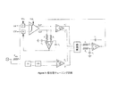
トランスコンダクタ及び減衰器に対して広帯域スケーリング情報を組み合せることにより、広帯域アナログプロセッサを構築するための基本となる構成単位または構成ブロックであるバイカッドを形成することができる。詳細には、本明細書で開示する、トランスコンダクタ、減衰器、およびスケーラブルな加算器を用いることにより、周波数アジャイルおよび/または時変である、プログラマブルバイカッド構造を形成することができる。このようなバイカッドを複数カスケード接続することにより、Guptaらの2009年3月10日が出願日である国際出願PCT/US2009/001512(国際公開WO2009/114123)に記載されているような、プログラマブル伝達関数シンセサイザを形成することができる。なお、この国際出願の全教示内容は、参照をもって本明細書に取り入れたものとする。バイカッドベースの回路により、アジャイルなフィルタ(agile filter)、等化器、遅延ラインなどを形成することができ、これらの最終用途としては、レーダ、コグニティブ無線、無線周波数識別(RFID)などが挙げられる。 By combining wideband scaling information for the transconductor and attenuator, a biquad that is the basic building block or building block for building a wideband analog processor can be formed. In particular, by using the transconductor, attenuator, and scalable adder disclosed herein, a programmable biquad structure that is frequency agile and / or time-varying can be formed. By cascading a plurality of such biquads, programmable transmission as described in International Application PCT / US2009 / 001512 (International Publication WO2009 / 114123) filed March 10, 2009 by Gupta et al. A function synthesizer can be formed. The entire teaching content of this international application is incorporated herein by reference. Biquad-based circuits can form agile filters, equalizers, delay lines, etc. These end uses include radar, cognitive radio, and radio frequency identification (RFID). It is done.
図1は、本発明の実施形態を適用可能なバイカッド回路100を示すブロック図である。バイカッド回路100は、その構成要素として、1つ以上の積分器110、1つ以上の減衰器120、および1つ以上の加算器130を備える。バイカッドの出力y(t)の特性は、バイカッド100の伝達関数T(s)を変更することによって変化できる。これは、a0,a1,b0,b1,b2で構成される減衰器120の数値を変更することによって達成される。積分器110のゲインGを変化させることにより、伝達関数の中心周波数を掃引できる。減衰器120の前記数値および積分器110の前記ゲインは、12ビットの精度を有するシリアルペリフェラルインターフェース(SPI)によってデジタル制御されてもよい。
FIG. 1 is a block diagram showing a
図2に、図1のバイカッド回路100に適用可能な積分器回路200を示す。積分器200は、フィードフォワード調節のトポロジを用いた、広帯域で自己チューニング型の積分器である。積分器200は、帯域幅が大きく、線形性が優れており、かつ、相互変調歪みが小さいので、マイクロ波周波数での用途に特に適している。
FIG. 2 shows an
小信号解析により、この回路の伝達関数は以下のように表される: By small signal analysis, the transfer function of this circuit is expressed as:

式中、 Where
通常、抵抗Rは、1/gm1,1/gm3,1/gds1,1/gds3に比べて小さくなるように選択される。ディープサブミクロンCMOS技術(例えば、130nm以下)の場合には、通常、Cgsが全寄生容量の大半を占める。これらを踏まえると、以下を導き出すことができる: Usually, the resistance R is selected to be smaller than 1 / g m1 , 1 / g m3 , 1 / g ds1 , 1 / g ds3 . For deep sub-micron CMOS technology (eg, 130 nm or less), C gs usually accounts for the majority of the total parasitic capacitance. Given these, the following can be derived:
fTはユニティゲイン周波数(単位利得周波数)であり、通常、その数値は大きい。小さい数値を有するRに比べて、通常、z2およびpは極めて大きい。これらを踏まえると、上記の伝達関数は、以下のように近似することができる: f T is a unity gain frequency (unit gain frequency), and its numerical value is usually large. Compared to R, which has a small numerical value, z 2 and p are usually very large. Given these, the above transfer function can be approximated as follows:
Rを、 R
と選択すると、a0=0となる。 If selected, a 0 = 0.
これにより、上記の伝達関数は、 Thus, the above transfer function becomes
とさらに簡略化することができる。 And can be further simplified.
上記の式は、理想的な積分器による応答を表す。通常、トランジスタは、gm1>gm3となるように選択される。したがって、 The above equation represents the response by an ideal integrator. Typically, the transistors are selected such that g m1 > g m3 . Therefore,
となる。 It becomes.
これは、積分器200のユニティゲイン周波数が、ディープサブミクロンCMOS技術のユニティゲイン周波数とほぼ同じであることを示している。
This indicates that the unity gain frequency of
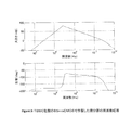
図3に、TMSC社製の65nmCMOSに適用された積分器200の周波数応答を示す。ユニティ周波数は約60GHzである。約10MHz〜60GHzにおいて20dB/decのゲインロールオフを示し、50MHz〜10GHzにおいて約−90°(±10°以内の変動あり)の位相を有する。
FIG. 3 shows the frequency response of the
図2に示す積分器回路200の実施形態には、様々な変更を施すことができる。図2の中間抵抗Rは、図4の積分器回路400のように、ゲートを電源に接続したトランジスタを用いて実現してもよい。この場合、その抵抗値(上記の伝達関数におけるa0の数値)の変更は、電圧を変化させるだけで行うことができる。つまり、ユーザは、フィードバック制御回路を用いることにより、積分器をチューニング(調節)することができる。この点については、後で説明する。
Various modifications can be made to the embodiment of the
図5に、積分器回路500の他の実施形態を示す。この実施形態では、図4のM2(およびM5)の抵抗が電圧VcRによって制御される。通常、M2(およびM5)の抵抗は、VcRが増加するにつれて減少する。VcRが過大にならないように、固定抵抗を、M2(およびM5)と並列に追加してもよい。
FIG. 5 shows another embodiment of
図6(a)〜(c)に、積分器回路601,602,603のさらなる他の実施形態を示す。図6(a)の積分器回路601のように、線形性をさらに向上させるために、上方に2つのソースディジェネレーション抵抗(ソース減衰抵抗)を追加してもよい。少し異なる手法として、図6(b)の積分器回路602のように、電流源を2つの同等な電流源に分割し、これら2つの電流源枝路間に単一のソースディジェネレーション抵抗を追加してもよい。図6(c)の積分器回路603は、上方及び下方の両方に、ソースディジェネレーション抵抗を有する。 6A to 6C show still other embodiments of the integrator circuits 601, 602, and 603. FIG. As in the integrator circuit 601 in FIG. 6A, two source degeneration resistors (source attenuation resistors) may be added above in order to further improve the linearity. A slightly different approach is to divide the current source into two equivalent current sources and add a single source degeneration resistor between these two current source branches, as in the integrator circuit 602 of FIG. 6 (b). May be. The integrator circuit 603 of FIG. 6C has source degeneration resistors both above and below.
図7に、積分器回路701(例えば、図2及び図4〜6を参照しながら説明した積分器回路)にチューニング回路702を組み合わせてなる、積分器チューニング回路700を示す。前述したように、電圧VcRの選択は、理想的な積分器を達成するために正確に行われる必要がある。このような選択は、チューニング回路702を介して行われる。このチューニング回路は、全体として、DC較正回路とゲイン制御回路の2つの部分を含む。当該DC較正回路の良好な動作のために、積分器の前段に、2つの同一のバッファ(例えば、ソースフォロワなど)が挿入される。一方のバッファは一定電圧Vfixでバイアスされており、他方のバッファはフィードバックループを介して制御される。なお、このフィードバックループは、前記積分器の差動出力を入力とする単なる積分回路である。このようなDC較正回路により、前記積分器の各差動出力のバイアス電圧は、確実に互いにほぼ同じとなる。この結果として、前記積分器は、チューニング(調節)後も高いコモンモード除去(同相分除去)を示す。
FIG. 7 shows an
電圧VcRが変化する際、低い周波数域ではDC較正後の積分器の位相が大きく変化する場合があり、また、当該位相は、電圧VcRに伴って単調に変化する。そのため、前記ゲイン制御回路は本質的には位相検出器であり、前記DC較正後の積分器が所与の低周波数において所望の位相応答を示すように当該DC較正後の積分器を駆動する。図7に示すように、発信器が200kHz信号を生成し、これが前記積分器に供給され、その出力が増幅される。同じ200kHz信号が移相器(PS)及びシングルトゥ差動変換器(単一差動変換器)(S2D)にも供給され、(前記積分器側の増幅器と同等な増幅器によって)増幅される。前記積分器側の増幅信号ならびに前記PS及びS2D側の増幅信号の双方が同じ乗算器に供給される。この乗算器のDC成分はこれら2つの増幅信号の位相差を示す。詳細には、前記2つの増幅信号の位相が合致している場合に前記乗算器のDC値は最大となり、前記2つの増幅信号の位相が互いに90°ずれている場合に前記乗算器のDC値がゼロとなる。前記移相器の位相値を適切に選択することにより、当該乗算器の後段に位置した別の積分回路が、200kHzにおいて前記積分器が所望の位相応答を示すように当該積分器を駆動する。つまり、その積分回路が電圧VcRの所望の数値を生成する。 When the voltage VcR changes, the phase of the integrator after DC calibration may change greatly in a low frequency range, and the phase changes monotonously with the voltage VcR. Thus, the gain control circuit is essentially a phase detector that drives the DC calibrated integrator so that the DC calibrated integrator exhibits a desired phase response at a given low frequency. As shown in FIG. 7, the oscillator generates a 200 kHz signal which is fed to the integrator and its output is amplified. The same 200 kHz signal is also fed to a phase shifter (PS) and a single-to-differential converter (single differential converter) (S2D) and amplified (by an amplifier equivalent to the amplifier on the integrator side). Both the amplified signal on the integrator side and the amplified signals on the PS and S2D side are supplied to the same multiplier. The DC component of this multiplier indicates the phase difference between these two amplified signals. Specifically, the DC value of the multiplier is maximized when the phases of the two amplified signals are matched, and the DC value of the multiplier is when the phases of the two amplified signals are 90 ° apart from each other. Becomes zero. By appropriately selecting the phase value of the phase shifter, another integrator circuit located after the multiplier drives the integrator so that the integrator exhibits a desired phase response at 200 kHz. That is, the integration circuit generates a desired numerical value of the voltage VcR.
図8に、減衰器回路800とその入力信号及び出力信号とを示す。減衰器は、プロセッサまたはDSPによって指定された所与のバイナリ数(二値数)に比例して信号を減衰する。減衰器には、「電圧線形的」および「dB線形的」の2種類がある。減衰器800は、「電圧線形的」な減衰器とされる。なお、「dB線形的」な減衰器は、dB単位で減衰される点を除けば「電圧線形的」な減衰器と同じである。
FIG. 8 shows the
減衰器の用途には、セルラーネットワークの信号処理要素、ケーブルモデムの信号処理要素、デジタル加入者回線の信号処理要素、撮像システムの信号処理要素、各種アプリケーションにおける適応フィルタの信号処理要素、および各種アプリケーションにおける等化器の信号処理要素が含まれる。マイクロ波部品市場では、数千万もの種類の減衰器が販売されており、さらにその何倍もの個数がVLSI(超大規模集積回路)設計に組み込まれている。 Applications of attenuators include cellular network signal processing elements, cable modem signal processing elements, digital subscriber line signal processing elements, imaging system signal processing elements, adaptive filter signal processing elements in various applications, and various applications Includes an equalizer signal processing element. In the microwave component market, tens of millions of types of attenuators are sold, and many times as many are incorporated into VLSI (Very Large Scale Integrated Circuit) designs.
図9に、R/2Rラダーを用いた典型的な減衰器900を示す。典型的な減衰器のデザインは、減衰器機能を実現するために多段式の抵抗ラダーを使用する。その段数は、減衰を制御するバイナリビット列(二値ビット列)に含まれるビット数と同じである。より高い精度を所望するほど、段数が増加し、公差が悪化する。そうなると、実現可能なダイナミックレンジも制限される。CMOS設計の場合、有用な抵抗ラダー構造は6〜8ビットに制限され、かつ、ダイナミックレンジも64〜256に制限される。レーザトリミングを用いれば高精度を実現可能であるが、コストが増加する。さらに、各段ごとに固有の帯域幅があるので、カスケード接続する段数が増加するほど、帯域幅が減少する。つまり、10ビット以上の精度を有する広帯域減衰器を低コストで実現したいのであれば、上記のような多段式の抵抗ラダーによるアーキテクチャは有用でない。
FIG. 9 shows a
図10に、本発明の一実施形態の減衰器回路1000を示す。この減衰器回路1000は、確率的設計手法を用いることにより、上述したような制限を克服している。この単一段の減衰器1000は、複数の抵抗Rからなる抵抗群で構成されている。抵抗Rは、(電源と出力の間の)直列アームと、(前記出力と接地の間の)負荷アームとの間で切り替えられる。各抵抗は、直列アームおよび負荷アームのいずれか一方に設定されている。
FIG. 10 illustrates an
前記複数の抵抗を、R,2R,4R,…,(2N)Rという比で構成することにより、Nビットの減衰器が得られることは言うまでもない。FETをオン状態かオフ状態のいずれかにしているスイッチは、一般に静電容量を有するため、大型の抵抗では帯域幅の問題が生じることを容易に予測できる。また、前記複数の抵抗のなかで最も小型の抵抗でさえも、そのインピーダンスがスイッチのインピーダンスよりも遥かに大きくなるように構成しなければならない。そのため、N>9にもなると、前記複数の抵抗のなかで最も大型の抵抗のサイズは極めて大きくなる。これは、広帯域性能に対する深刻な問題である。また、大型の抵抗のサイズが極めて大きくなると、それに伴って多くのシリコン領域が消費されてしまう。さらに、幅広い範囲の抵抗値に対応するには、1種類のモデルの抵抗器では十分な抵抗の範囲をカバーできないので、複数の異なるファミリーの抵抗器を使用する必要が生じる。異なるモデルの抵抗器は互いに異なる温度係数を有するため、特に温度変化等により、精度が低下してしまう。 It goes without saying that an N-bit attenuator can be obtained by configuring the plurality of resistors at a ratio of R, 2R, 4R,..., (2N) R. Since a switch that has an FET in either an on state or an off state generally has a capacitance, it can be easily predicted that a bandwidth problem will occur in a large resistor. Further, even the smallest resistor among the plurality of resistors must be configured so that its impedance is much larger than the impedance of the switch. Therefore, when N> 9, the size of the largest resistor among the plurality of resistors becomes extremely large. This is a serious problem for wideband performance. Further, when the size of the large resistor becomes extremely large, a large amount of silicon region is consumed accordingly. Furthermore, to accommodate a wide range of resistance values, one type of resistor cannot cover a sufficient resistance range, necessitating the use of a plurality of different families of resistors. Since the resistors of different models have different temperature coefficients, the accuracy is deteriorated particularly due to a temperature change or the like.
帯域幅の問題は、FETスイッチのサイズを抵抗器のサイズに対して反比例するように選択し、各アームのRC時定数を互いに同じとすることにより、軽減することができる。理論的には、これによって帯域幅が無限大になるはずである。しかし、最も小型のFETに対して最も大型のFETの比が極めて大きくなり、今度はレイアウト及びシリコンサイズの問題が生じる。その理由は、最も小型の抵抗に対するミスマッチ関連の変動(variation)を抑えるために、最も小型のFETを十分に大きく形成しなければならないからである。 Bandwidth problems can be mitigated by selecting the FET switch size inversely proportional to the resistor size and making the RC time constants of each arm the same. Theoretically, this should make the bandwidth infinite. However, the ratio of the largest FET to the smallest FET becomes very large, which in turn causes layout and silicon size issues. The reason is that the smallest FET must be made large enough to suppress mismatch related variations to the smallest resistor.
減衰器1000は、N個の抵抗を用いて2N種類(2N個)の減衰値(減衰量)を提供する。このような減衰器は、N種類の数値設定が可能なので、N個の自由度を有する。理想的な減衰器であれば、数直線0〜1の間で2N個の等間隔の減衰点を有するはずである。つまり、減衰値は、0〜1までの区間で一様に分布するはずである(1/2N個のビン化が可能になるはずである)。理想的でない状況では、多くのビンが空で、別の多くのビンに複数の数値が含まれる。レーザトリミングを用いれば、前記分布を変化させて全てのビンに数値が含まれるように減衰値を移動させることも可能である。しかし、これは困難かつ高コストである。
The
図11に、減衰器回路1100の他の実施形態を示す。一部の実施形態では、M個の自由度(M個の抵抗)がある。ただし、M>Nである。この場合、0〜1までの区間において、2M個の点を生成することができる。M個の抵抗を適切に選択することにより、2N個のビンの各ビンに複数の点が含まれるように分布を形成することができる。さらに、この後、抵抗/FETの公差を含めてモンテカルロシミュレーションを行い、それらの公差を加味したうえでも各ビンに少なくとも1つの点が含まれる分布が高確率で得られるようにしてもよい。さらに、このようにして得られた結果を2M個の点の全ての点について確認することによって較正し、2N個の所望値に対応するM個の制御ビットの組合せを決定してもよい。このM個の制御ビットの組合せのテーブルは、Mビットの長さを有するワードを2N個収容可能なサイズのメモリに記憶してもよい。所望の減衰値に応じてN個のアドレスラインが形成されたメモリは、対応するM個のビットからなる数値を減衰器に向けて(データバス上に)送出し、当該減衰器に所望の減衰を行わせる。N*ビットの精度を所望し(N<N*<M)、かつ、ミッシングコード(例えば、0近傍の数値または1近傍の数値)が幾つか存在しても構わない場合、Mビットの長さを有するワードを2N*個収容できるサイズのメモリに、プログラムを組み込んでもよい。このような実施形態を、図11の減衰器回路1100で示す。 FIG. 11 illustrates another embodiment of an attenuator circuit 1100. In some embodiments, there are M degrees of freedom (M resistors). However, M> N. In this case, 2M points can be generated in the interval from 0 to 1. By appropriately selecting M resistors, a distribution can be formed such that a plurality of points are included in each bin of 2 N bins. Further, after this, Monte Carlo simulation including resistance / FET tolerance may be performed, and distribution including at least one point in each bin may be obtained with high probability even considering the tolerance. Further, the result thus obtained may be calibrated by checking for all of the 2M points to determine a combination of M control bits corresponding to 2N desired values. . The table of combinations of M control bits may be stored in a memory having a size that can accommodate 2N words having a length of M bits. A memory in which N address lines are formed according to a desired attenuation value sends a numerical value consisting of the corresponding M bits to the attenuator (on the data bus), and the desired attenuation is transmitted to the attenuator. To do. Length of M bits if N * bit accuracy is desired (N <N * <M) and there are some missing codes (for example, numerical values near 0 or numerical values near 1) The program may be incorporated in a memory of a size that can accommodate 2N * words having the word "." Such an embodiment is illustrated by the attenuator circuit 1100 of FIG.
図12(a)に、Nビットの精度を有する減衰器回路によって達成される減衰の分布の一例を示す。この減衰器回路は、抵抗R,2R,…,(2N)Rを有するM個の自由度のネットワークを具備する。図12(b)に、図12(a)の各抵抗の数値を1−x/100から1+x/100までの範囲内で一様に分布したランダム変数(x%の誤差)によってディザリング(変更)した場合の制御ビットパターンの典型的な一例を示す。図12(b)の減衰の分布は、図12(a)の数値の周りに分散している。この方法を用いると、数値が集中した幾つかのビン(特に、そのような複数のビンのうちの中央のビン)の近傍に位置する空のビンにも、数値を埋めることができる。このような手法は、「分布の円滑化」と称される。 FIG. 12A shows an example of an attenuation distribution achieved by an attenuator circuit having N-bit accuracy. The attenuator circuit comprises a network of M degrees of freedom having resistors R, 2R,..., (2N) R. 12B is dithered (changed) by the random variable (x% error) in which the numerical values of the resistors in FIG. 12A are uniformly distributed within the range from 1-x / 100 to 1 + x / 100. ) Shows a typical example of the control bit pattern. The attenuation distribution in FIG. 12B is distributed around the numerical values in FIG. By using this method, it is possible to fill a numerical value even in an empty bin located in the vicinity of several bins in which numerical values are concentrated (particularly, a central bin among such a plurality of bins). Such a technique is referred to as “smooth distribution”.
図13に、Nビット(この例ではN=12)の精度を有する、Mビット減衰器1300(この例ではM=24)を示す。抵抗間(すなわち、FETスイッチ間)の最大の比は約64とする。まず抵抗R,2R,4R,8R,16R,32R,64Rから始め、次に数2,4,8,16,32に対する素数59,53,47,43,41,37,31に相当する抵抗59R,53R,47R,43R,41R,37R,31Rを追加する。このようにして得られる分布にx=5%のディザリングを施し、2N個のビンの最も良好な分布(最大範囲の埋まり)を求める。次に、M個の抵抗が揃うまで、抵抗値Rを追加する(この例では、10種類の抵抗値Rを追加する)。
FIG. 13 shows an M-bit attenuator 1300 (M = 24 in this example) having an accuracy of N bits (N = 12 in this example). The maximum ratio between resistors (ie, between FET switches) is about 64. First, resistors R, 2R, 4R, 8R, 16R, 32R, and 64R, and then resistors 59R corresponding to primes 59, 53, 47, 43, 41, 37, and 31 for the
図14に、N=10、N=12およびN=14で得られる分布を示す。モンテカルロシミュレーションによると、65nmCMOS技術において最小抵抗器のサイズがR=100Ωで最小FETのサイズが0.12μmである場合のミスマッチに起因するFET及び抵抗の変動は約1.5%と算出される。x=2%で長時間シミュレーションを実行すると、500組のデザインのうちの全てにおいて、N=12の場合に212のビンのうちの最小ビン0および最大ビン1023を除く全てのビンが0〜1までの範囲内の要素を少なくとも1つ有するという要件が満たされた。
FIG. 14 shows the distribution obtained with N = 10, N = 12, and N = 14. According to the Monte Carlo simulation, in the 65 nm CMOS technology, when the size of the minimum resistor is R = 100Ω and the size of the minimum FET is 0.12 μm, the variation in FET and resistance due to mismatch is calculated to be about 1.5%. When you run a long simulation x = 2%, all of the 500 sets of design, in the case of N = 12 for all bins except the
図15に、特定の損失パターンを有する減衰器1300の周波数領域性能を示す。概して言えば、この減衰器は、帯域幅の上限が10GHzを超えると減衰値に変化が生じる。 FIG. 15 shows the frequency domain performance of an attenuator 1300 having a specific loss pattern. Generally speaking, the attenuation value of the attenuator changes when the upper limit of the bandwidth exceeds 10 GHz.
特定の減衰器を較正する場合、まず名目上のデザインから始める。複数のビンからなるテーブルを生成し、各ビンにわたって分布した制御ビットの組合せを最大10組生成する。当然ながら、制御ビットの組合せが10に満たないビンでは、前記最大10個の組合せにおいて、その全ての要素がリストアップされる。 When calibrating a specific attenuator, start with a nominal design. A table composed of a plurality of bins is generated, and a maximum of 10 combinations of control bits distributed over each bin are generated. Of course, in a bin where the number of combinations of control bits is less than 10, all the elements are listed in the maximum of 10 combinations.
減衰器を較正する際、まずビンi(1≦i≦2N)から始め、そのビンにおける名目上の制御ビットパターンに注目する。達成される実際の減衰を測定し、誤差を算出する。この誤差に2Nを乗算し、当該誤差を補正するのにシフトしなければならないビンの数を決定する。このシフト方向は、前記誤差の正負によって決まる。実際の減衰の測定値が高過ぎると、ビン番号の小さい方向にシフトさせ、当該測定値が低過ぎると、ビン番号の大きい方向にシフトさせる。新たな制御ビットパターンを決定した後は(選択したビンにおいて一部の制御パターンが他の制御パターンよりも優れた数値を複数生成するような場合、そのなかで最も優れた制御パターンを保持する)、所望の精度が得られるまで、上記過程をさらに繰り返す。実際的には、2〜3回のステップで所望の精度を得ることができる。 When calibrating the attenuator, start with bin i (1 ≦ i ≦ 2N) and focus on the nominal control bit pattern in that bin. Measure the actual attenuation achieved and calculate the error. This error is multiplied by 2N to determine the number of bins that must be shifted to correct the error. This shift direction is determined by the sign of the error. If the actual measured value of attenuation is too high, it is shifted in the direction of decreasing bin number, and if the measured value is too low, it is shifted in the direction of increasing bin number. After determining a new control bit pattern (if some of the control patterns in the selected bin generate multiple values that are better than others, retain the best control pattern among them) The above process is further repeated until the desired accuracy is obtained. In practice, the desired accuracy can be obtained in two to three steps.
上記過程の全体を、2N個のビンの数値からなる完全なテーブルおよび対応する制御ビットパターンが得られるまで、全てのビンについて繰り返す。 The entire process is repeated for all bins until a complete table of 2 N bin values and the corresponding control bit pattern is obtained.
上述した方法により、高精度かつ低コストで、大きい帯域幅および優れた歩留まりを有するCMOS減衰器を提供することができる。Nビットの精度を所望する場合、まず、M個の抵抗およびM個のスイッチから始める(M>N)。Mの数値をNの数値よりも十分大きく選択することにより、部品公差を加味したうえでもNビットの精度を満たす減衰器が高確率で得られることを統計学的に「保証」することができるので、十分な高精度を実現できる。また、その製造プロセスにレーザトリミングは不要である。 The above-described method can provide a CMOS attenuator having high bandwidth and excellent yield with high accuracy and low cost. If N-bit accuracy is desired, start with M resistors and M switches (M> N). By selecting the value of M sufficiently larger than the value of N, it is possible to statistically “guarantee” that an attenuator satisfying the accuracy of N bits can be obtained with high probability even considering the component tolerance. Therefore, sufficient high accuracy can be realized. Further, laser trimming is not necessary in the manufacturing process.
以上のように、最適な分布を得るための抵抗の選択方法を開示した。また、特定の構成の減衰器を得るための減衰器の較正方法を開示した。なお、前述の例示的な実施形態では「電圧線形的」な減衰器を形成したが、当業者であれば、同じ方法を用いて「dB線形的」な減衰器を形成することができる。 As described above, a method for selecting a resistor for obtaining an optimum distribution has been disclosed. Also disclosed is an attenuator calibration method for obtaining an attenuator of a specific configuration. Note that although the “voltage linear” attenuator is formed in the exemplary embodiment described above, those skilled in the art can form a “dB linear” attenuator using the same method.
図16に、図1を参照しながら説明したバイカッド回路100に適用可能な加算回路1600を示す。加算回路1600は、単一の抵抗RとN個のトランジスタとを有する。加算器1600は、広帯域アナログ信号処理を必要とする回路トポロジに使用できる。トランジスタの数であるNは、加算される入力信号の数によって決まる。
FIG. 16 shows an adder circuit 1600 applicable to the
この加算器は、入力信号V1,V2,…,VNを受け取り、出力信号Voutを生成する。これら入力信号V1,V2,…,VNおよび出力信号Voutは、いずれもDC項とAC項の両方を含む。抵抗Rにより、加算回路網を通るDC電流が設定される。つまり、抵抗Rは、加算ブロックの総合ゲインに寄与する。重ね合わせの原理を用いて、1度に1個のトランジスタを考慮すると、単一のソース接地(CS)増幅器についての分析だけで済む。出力におけるDCバイアス項を無視してAC項のみに注目すると、前記CS増幅器の出力は以下のように表される: This adder receives input signals V 1 , V 2 ,..., V N and generates an output signal V out . These input signals V 1 , V 2 ,..., V N and the output signal V out all include both a DC term and an AC term. Resistor R sets the DC current through the summing network. That is, the resistor R contributes to the total gain of the addition block. Using the superposition principle and considering one transistor at a time, only analysis on a single source grounded (CS) amplifier is required. If we ignore the DC bias term in the output and focus only on the AC term, the output of the CS amplifier is expressed as:
![]()
![]()
式1において、gmはトランジスタのゲイン(すなわち、トランスコンダクタンス)であり、roはトランジスタの出力抵抗である。ro>>Rと仮定すると、図16の回路の総出力は以下のように表される:
In
![]()
![]()
式2において、対応する入力信号vに付随する各gm項は、加算係数と見なすことができる。抵抗Rは一定なので、トランジスタのゲインgmを変化させることにより、前記加算係数を調整することができる。トランジスタのゲインgmは、トランジスタの幅Wを用いて以下のように表すことができる:
In
式3によると、トランジスタのゲインはトランジスタの幅に正比例する。したがって、トランジスタの幅を変化させることにより、加算係数を調整することができる。 According to Equation 3, the gain of the transistor is directly proportional to the width of the transistor. Therefore, the addition coefficient can be adjusted by changing the width of the transistor.
加算回路1600の帯域幅は、前記CS増幅器の帯域幅によって決まる。図17に、CS増幅器の高周波数挙動の分析に一般的に利用される、等価的な小信号回路モデル1700を示す。抵抗RTはR‖ro(RT=Rro/(R+ro))で与えられ、容量CTはトランジスタの出力ノードと接地との間の容量の総計(すなわち、負荷容量とトランジスタ内部の寄生容量と後続段の入力容量との合計)である。 The bandwidth of the adding circuit 1600 is determined by the bandwidth of the CS amplifier. FIG. 17 shows an equivalent small signal circuit model 1700 that is commonly used to analyze the high frequency behavior of a CS amplifier. The resistance R T is given by R‖r o (R T = Rr o / (R + r o )), and the capacitance C T is the sum of the capacitance between the output node of the transistor and ground (ie, the load capacitance The sum of the parasitic capacitance and the input capacitance of the subsequent stage).
Rsが比較的大きく、かつ、CTが比較的小さい場合、前記CS増幅器の帯域幅は以下のように表される: When R s is relatively large and CT is relatively small, the bandwidth of the CS amplifier is expressed as:
![]()
![]()
Rsが比較的小さい場合、前記CS増幅器の帯域幅は以下のように表される: If R s is relatively small, the bandwidth of the CS amplifier is expressed as:
![]()
![]()
上記の式から、(RTはR‖roで与えられるので、)Rが小さい場合、帯域幅が大きくなることが分かる。通常これは損失につながる。当該損失の軽減、つまりゲインの向上を達成するには、Rを増加させる必要があるが、通常これは帯域幅の減少という妥協を伴う。 From the above equations, (because it is given by R T is R‖r o,) if R is small, it can be seen that the bandwidth is increased. This usually leads to loss. To achieve this loss mitigation, ie gain improvement, R needs to be increased, but this usually involves a compromise of bandwidth reduction.
TSMC社の65nmプロセスを用いてCadence社によって作製された3入力加算回路を用意した。図18に、電源抵抗Rsを10Ωとした場合のこの回路の周波数応答を示す。図中の実線は、R=26Ωの場合に相当する。この場合の回路では、損失は5.4dBとなる一方で、3dB帯域幅は約200GHzとなる。図中の破線は、R=60Ωの場合に相当する。この場合の回路では、損失はほぼ0dBである一方で、3dB帯域幅は90GHzに減少する。 A three-input adder circuit made by Cadence using a TSMC 65 nm process was prepared. FIG. 18 shows the frequency response of this circuit when the power supply resistance Rs is 10Ω. The solid line in the figure corresponds to the case of R = 26Ω. In the circuit in this case, the loss is 5.4 dB, while the 3 dB bandwidth is about 200 GHz. The broken line in the figure corresponds to the case of R = 60Ω. In the circuit in this case, the loss is approximately 0 dB, while the 3 dB bandwidth is reduced to 90 GHz.
図19に、前述した積分器、減衰器および加算器の実施形態を適用可能な、直列接続した複数のバイカッド回路1900を示す。このバイカッド構造は二次の状態変数構造である。N個のバイカッドをカスケード接続することにより、2N次の伝達関数T(s)’が得られる。 FIG. 19 illustrates a plurality of biquad circuits 1900 connected in series to which the integrator, attenuator, and adder embodiments described above can be applied. This biquad structure is a secondary state variable structure. By cascading N biquads, a 2Nth order transfer function T (s) 'is obtained.
図19に示す伝達関数は、単入力単出力(SISO)のフィールドプログラマブルアナログアレイ(FPAA)を記述しているとも見なせる。減衰器の数値および積分器のゲインを変化させることにより、様々な適応フィルタ特性および遅延ライン特性を実現できる。アナログ領域において動作可能なため、エンジニアにとって広帯域信号を処理するための強力なツールとなる。 The transfer function shown in FIG. 19 can also be regarded as describing a single input single output (SISO) field programmable analog array (FPAA). Various adaptive filter characteristics and delay line characteristics can be realized by changing the numerical value of the attenuator and the gain of the integrator. Being able to operate in the analog domain makes it a powerful tool for engineers to process wideband signals.
以上のとおり、本発明を好ましい実施形態に基づいて具体的に図示し詳細に説明した。しかし、当業者であれば、添付の特許請求の範囲に包含される本発明の範囲を逸脱することなく形態および細部に対して様々な変更が可能であることを理解するであろう。
なお、以下に、本発明の必須の構成要素を含まない態様について説明する。
〔態様1〕
広帯域アナログ無線周波数の減衰器であって、
M個からなる複数の減衰器ブロックを備え、これらブロックは、それぞれ、
信号レールと出力ノードとの間に接続された第1のスイッチと、
オフセットレールと前記出力ノードとの間に接続された第2のスイッチと、
前記出力ノードと前記第1及び第2のスイッチとの間に直列接続された抵抗要素とを含み、
当該減衰器ブロックが、Nビットの精度であって、NがMよりも小さい、精度をもたらす、広帯域アナログ無線周波数の減衰器。
〔態様2〕
態様1に記載の減衰器において、前記ブロックのうちの少なくとも1つにおける抵抗要素の抵抗値が、前記ブロックのうちの他の1つのブロックにおける抵抗値に対する素数に相当する、広帯域アナログ無線周波数の減衰器。
〔態様3〕
態様1に記載の減衰器において、前記ブロックのそれぞれの前記抵抗要素の数値が、一様に分布したランダム変数によってディザリングされたものである、広帯域アナログ無線周波数の減衰器。
〔態様4〕
態様1に記載の減衰器において、前記出力ノードで計測された誤差に基づいて前記第1及び第2のスイッチを制御するプログラム入力を設定することによって、較正が行われる、広帯域アナログ無線周波数の減衰器。
〔態様5〕
態様1に記載の減衰器において、相補型金属酸化膜半導体技術、または絶縁体上シリコン技術を用いて作製された、広帯域アナログ無線周波数の減衰器。
〔態様6〕
広帯域アナログ無線周波数のスケーラブルな加算器であって、
出力ノードと接地レールとの間に並列接続された、N個からなる複数のスイッチと、
電源レールと前記出力ノードとの間に直列接続された抵抗要素とを備え、
前記スイッチのそれぞれが、それぞれ対応する電圧入力によって制御される、広帯域アナログ無線周波数のスケーラブルな加算器。
〔態様7〕
態様6に記載の加算器において、前記Nが、加算すべき入力信号の数に基づいて決定される、広帯域アナログ無線周波数のスケーラブルな加算器。
〔態様8〕
態様6に記載の加算器において、相補型金属酸化膜半導体技術、または絶縁体上シリコン技術を用いて作製された、広帯域アナログ無線周波数のスケーラブルな加算器。
As described above, the present invention has been specifically illustrated and described in detail based on the preferred embodiments. However, one of ordinary skill in the art appreciates that various changes can be made in form and detail without departing from the scope of the invention as encompassed by the appended claims.
In addition, the aspect which does not contain the essential component of this invention below is demonstrated.
[Aspect 1]
A broadband analog radio frequency attenuator comprising:
A plurality of M attenuator blocks, each of which is
A first switch connected between the signal rail and the output node;
A second switch connected between an offset rail and the output node;
A resistive element connected in series between the output node and the first and second switches;
A wideband analog radio frequency attenuator, wherein the attenuator block provides N bits of precision, N being less than M.
[Aspect 2]
The attenuator according to
[Aspect 3]
The attenuator according to
[Aspect 4]
Attenuator of
[Aspect 5]
The attenuator according to
[Aspect 6]
A wideband analog radio frequency scalable adder,
A plurality of N switches connected in parallel between the output node and the ground rail;
A resistance element connected in series between a power supply rail and the output node;
A broadband analog radio frequency scalable adder, wherein each of the switches is controlled by a corresponding voltage input.
[Aspect 7]
The adder according to
[Aspect 8]
The adder according to
Claims (8)
第1及び第2のpチャネルトランジスタであって、それぞれ、第1の電圧供給端子に並列に接続されたソース、およびドレインを有し、当該第1のpチャネルトランジスタの前記ドレインと、当該第2のpチャネルトランジスタの前記ドレインとが、互いに相補的な出力信号を提供する、第1及び第2のpチャネルトランジスタと、
第1及び第2の可変抵抗手段であって、
第1の可変抵抗手段は前記第1のpチャネルトランジスタのドレインに接続された第1端子および第2端子を有し、
第2の可変抵抗手段は前記第2のpチャネルトランジスタのドレインに接続された第1端子および第2端子を有する、第1及び第2の可変抵抗手段と、
第1及び第2のnチャネルトランジスタであって、
第1のnチャネルトランジスタは前記第1の可変抵抗手段の前記第2端子に接続されたドレイン、ゲート、および第2の電圧供給端子に電気的に導通したソースを有し、
第2のnチャネルトランジスタは前記第2の可変抵抗手段の前記第2端子に接続されたドレイン、ゲート、および第2の電圧供給端子に電気的に導通したソースを有し、
当該第1のnチャネルトランジスタの前記ゲートと、当該第2のnチャネルトランジスタの前記ゲートとが、互いに相補的な入力信号を受け取る、第1及び第2のnチャネルトランジスタと、
当該積分器の出力の位相を調整するチューニング回路とを備えた、広帯域アナログ無線周波数の積分器。 A broadband analog radio frequency integrator,
First and second p-channel transistors each having a source and a drain connected in parallel to a first voltage supply terminal, the drain of the first p-channel transistor, and the second First and second p-channel transistors, wherein the drains of the p-channel transistors provide complementary output signals;
First and second variable resistance means,
The first variable resistance means having a first terminal and a second terminal connected to the drain of said first p-channel transistor,
The second variable resistance means having a first terminal and a second terminal connected to the drain of said second p-channel transistor, and the first and second variable resistance means,
First and second n-channel transistors,
A first n-channel transistor having a drain connected to the second terminal of the first variable resistance means, a gate, and a source electrically connected to a second voltage supply terminal;
A second n-channel transistor having a drain connected to the second terminal of the second variable resistance means, a gate, and a source electrically connected to a second voltage supply terminal;
First and second n-channel transistors, wherein the gate of the first n-channel transistor and the gate of the second n-channel transistor receive complementary input signals ;
A broadband analog radio frequency integrator comprising a tuning circuit for adjusting a phase of an output of the integrator.
前記第2の電圧供給端子と前記第1及び第2のnチャネルトランジスタのソースとの間に直列接続されたバイアス抵抗を備えた、広帯域アナログ無線周波数の積分器。 The integrator of claim 1, further comprising:
A wideband analog radio frequency integrator comprising a bias resistor connected in series between the second voltage supply terminal and the sources of the first and second n-channel transistors.
前記第1および第2の可変抵抗手段がそれぞれ第3及び第4のpチャネルトランジスタからなり、
さらに、
前記第3及び第4のpチャネルトランジスタのゲートに電気的に導通して当該第1及び第2の可変抵抗手段の抵抗を制御する第3の電圧供給端子を備えた、広帯域アナログ無線周波数の積分器。 The integrator of claim 1,
The first and second variable resistance means comprise third and fourth p-channel transistors, respectively;
further,
Wideband analog radio frequency integration comprising a third voltage supply terminal electrically connected to the gates of the third and fourth p- channel transistors to control the resistance of the first and second variable resistance means. vessel.
前記第1の可変抵抗手段が第3のpチャネルトランジスタからなり、
前記第2の可変抵抗手段が第4のpチャネルトランジスタからなり、
前記第3のpチャネルトランジスタは、前記第1のnチャネルトランジスタのドレインに接続されたドレイン、前記第2のnチャネルトランジスタのゲートに接続されたソース、およびゲートを有し、
前記第4のpチャネルトランジスタは、前記第2のnチャネルトランジスタのドレインに接続されたドレイン、前記第1のnチャネルトランジスタのゲートに接続されたソース、およびゲートを有し、
前記第3のpチャネルトランジスタのゲートと前記第4のpチャネルトランジスタのゲートとが互いに接続されている、広帯域アナログ無線周波数の積分器。 The integrator of claim 1,
It said first variable resistor means comprises a third p-channel transistor,
The second variable resistance means comprises a fourth p-channel transistor,
The third p-channel transistor, the first n-channel drain connected to the drain of the transistor, the second n-channel source connected to the gate of the transistor, and a gate,
The fourth p-channel transistor, said second n-channel drain connected to the drain of the transistor, the first n-channel source connected to the gate of the transistor, and a gate,
A broadband analog radio frequency integrator, wherein a gate of the third p- channel transistor and a gate of the fourth p- channel transistor are connected to each other.
前記第3の電圧供給端子から供給される電圧が、前記チューニング回路から選択される、広帯域アナログ無線周波数の積分器。 A broadband analog radio frequency integrator, wherein a voltage supplied from the third voltage supply terminal is selected from the tuning circuit.
Applications Claiming Priority (5)
| Application Number | Priority Date | Filing Date | Title |
|---|---|---|---|
| US30406410P | 2010-02-12 | 2010-02-12 | |
| US61/304,064 | 2010-02-12 | ||
| US35910810P | 2010-06-28 | 2010-06-28 | |
| US61/359,108 | 2010-06-28 | ||
| PCT/US2011/024542 WO2011152896A1 (en) | 2010-02-12 | 2011-02-11 | Broadband analog radio-frequency components |
Publications (3)
| Publication Number | Publication Date |
|---|---|
| JP2013520101A JP2013520101A (en) | 2013-05-30 |
| JP2013520101A5 JP2013520101A5 (en) | 2015-07-02 |
| JP5870368B2 true JP5870368B2 (en) | 2016-03-01 |
Family
ID=45067016
Family Applications (1)
| Application Number | Title | Priority Date | Filing Date |
|---|---|---|---|
| JP2012553037A Expired - Fee Related JP5870368B2 (en) | 2010-02-12 | 2011-02-11 | Components that process wideband analog radio frequencies |
Country Status (6)
| Country | Link |
|---|---|
| US (1) | US8866531B2 (en) |
| EP (1) | EP2522073A4 (en) |
| JP (1) | JP5870368B2 (en) |
| KR (1) | KR101310418B1 (en) |
| CN (1) | CN102835027B (en) |
| WO (1) | WO2011152896A1 (en) |
Families Citing this family (14)
| Publication number | Priority date | Publication date | Assignee | Title |
|---|---|---|---|---|
| EP2253066B1 (en) | 2008-03-10 | 2016-05-11 | Spero Devices, Inc. | Method, system, and apparatus for wideband signal processeing |
| JP5870368B2 (en) | 2010-02-12 | 2016-03-01 | スペロ・デバイシーズ・インコーポレーテッド | Components that process wideband analog radio frequencies |
| US9007128B2 (en) | 2010-11-01 | 2015-04-14 | Newlans, Inc. | Method and apparatus for power amplifier linearization |
| WO2012064551A2 (en) | 2010-11-08 | 2012-05-18 | Newlans, Inc. | Field programmable analog array |
| CN103959726A (en) | 2011-11-01 | 2014-07-30 | 纽兰斯公司 | Wideband signal processing |
| WO2013138457A1 (en) | 2012-03-15 | 2013-09-19 | Newlans, Inc. | Software-defined radio with broadband amplifiers and antenna matching |
| KR20150053784A (en) * | 2012-09-05 | 2015-05-18 | 뉴랜스, 인코포레이티드. | Bi-quad calibration |
| CN104348445A (en) * | 2013-07-26 | 2015-02-11 | 中兴通讯股份有限公司 | Attenuation device, system and attenuation method |
| US9130547B1 (en) * | 2014-07-17 | 2015-09-08 | Realtek Semiconductor Corp. | Rail-to-rail comparator circuit and method thereof |
| US10267896B1 (en) * | 2014-08-21 | 2019-04-23 | National Technology & Engineering Solutions Of Sandia, Llc | Variable bandwidth filter |
| CN104378104B (en) * | 2014-09-28 | 2017-04-26 | 宁波大学 | CMOS addition unit |
| US9832048B2 (en) * | 2015-08-24 | 2017-11-28 | Xilinx, Inc. | Transmitter circuit for and methods of generating a modulated signal in a transmitter |
| US11017184B2 (en) * | 2018-10-26 | 2021-05-25 | Sendyne Corporation | Runtime-calibratable analog computing system and methods of use |
| CN115642971B (en) * | 2022-12-22 | 2023-05-09 | 成都华兴汇明科技有限公司 | Simulation file generation method and automatic extraction system for nonlinear parameters of microwave module |
Family Cites Families (64)
| Publication number | Priority date | Publication date | Assignee | Title |
|---|---|---|---|---|
| US3434060A (en) | 1964-10-14 | 1969-03-18 | Lockheed Aircraft Corp | Damped shock spectrum filter |
| US4086539A (en) | 1972-08-11 | 1978-04-25 | Massachusetts Institute Of Technology | First-order phase-lock loop |
| US3978416A (en) | 1975-04-30 | 1976-08-31 | Rca Corporation | Filter which tracks changing frequency of input signal |
| US4179665A (en) | 1978-09-08 | 1979-12-18 | American Microsystems, Inc. | Switched capacitor elliptic filter |
| DE3204430A1 (en) * | 1982-02-09 | 1983-08-18 | Siemens AG, 1000 Berlin und 8000 München | INTEGRABLE DIFFERENTIAL AMPLIFIER |
| US4507791A (en) | 1982-05-05 | 1985-03-26 | Dolby Laboratories Licensing Corporation | Analog and digital signal apparatus |
| JPH07118617B2 (en) | 1990-07-19 | 1995-12-18 | 沖電気工業株式会社 | Power amplifier and transmitter |
| US5229664A (en) * | 1991-07-03 | 1993-07-20 | Exar Corporation | Programmable differentiator delay |
| US5325204A (en) | 1992-05-14 | 1994-06-28 | Hitachi America, Ltd. | Narrowband interference cancellation through the use of digital recursive notch filters |
| EP0579875B1 (en) | 1992-07-24 | 1997-09-10 | Alcatel | Quality factor tuning system |
| WO1995005027A1 (en) * | 1993-08-10 | 1995-02-16 | Fujitsu Limited | Low-current amplifier |
| US5959871A (en) | 1993-12-23 | 1999-09-28 | Analogix/Portland State University | Programmable analog array circuit |
| US20010055320A1 (en) | 1994-12-15 | 2001-12-27 | Pierzga Wayne Francis | Multiplex communication |
| GB2340003B (en) * | 1994-12-15 | 2000-03-22 | Inmarsat Ltd | Multiplex communication |
| AU4400096A (en) * | 1995-01-12 | 1996-07-31 | Takeshi Ikeda | Tuning circuit |
| US5574678A (en) | 1995-03-01 | 1996-11-12 | Lattice Semiconductor Corp. | Continuous time programmable analog block architecture |
| GB2317537B (en) | 1996-09-19 | 2000-05-17 | Matra Marconi Space | Digital signal processing apparatus for frequency demultiplexing or multiplexing |
| US5912583A (en) * | 1997-01-02 | 1999-06-15 | Texas Instruments Incorporated | Continuous time filter with programmable bandwidth and tuning loop |
| US5880637A (en) * | 1997-05-05 | 1999-03-09 | Motorola, Inc. | Low-power operational amplifier having fast setting time and high voltage gain suitable for use in sampled data systems |
| JP4086371B2 (en) * | 1998-08-18 | 2008-05-14 | 富士通株式会社 | Semiconductor amplifier circuit |
| US6307427B1 (en) * | 1998-08-06 | 2001-10-23 | Fujitsu Limited | Filter characteristic regulating apparatus and regulating method therefor |
| JP3776680B2 (en) * | 1999-06-18 | 2006-05-17 | 株式会社東芝 | Voltage controlled oscillator and signal processing circuit |
| US6359507B1 (en) * | 1999-08-18 | 2002-03-19 | Lucent Technologies Inc. | Method and apparatus for an automatic predistortion system |
| WO2001047762A1 (en) | 1999-12-29 | 2001-07-05 | Delphi Technologies, Inc. | Method and system for improving motor vehicle stability incorporating an electric power steering system |
| US6424209B1 (en) | 2000-02-18 | 2002-07-23 | Lattice Semiconductor Corporation | Integrated programmable continuous time filter with programmable capacitor arrays |
| JP2001251163A (en) * | 2000-03-07 | 2001-09-14 | Sony Corp | Differential input-output integrator for low frequency, differential input-output integrator for high frequency and current drive differential input-output integrator |
| US7123177B2 (en) | 2000-11-17 | 2006-10-17 | Broadcom Corporation | System and method for stabilizing high order sigma delta modulators |
| IL158717A0 (en) | 2001-05-04 | 2004-05-12 | Lockheed Corp | System and method for wideband pre-detection signal processing for passive coherent location applications |
| US7158591B2 (en) | 2001-05-09 | 2007-01-02 | Signum Concept, Inc. | Recursive resampling digital filter structure for demodulating 3G wireless signals |
| US7061944B2 (en) * | 2001-05-25 | 2006-06-13 | International Business Machines Corporation | Apparatus and method for wavelength-locked loops for systems and applications employing electromagnetic signals |
| JP2002374179A (en) | 2001-06-12 | 2002-12-26 | Hitachi Kokusai Electric Inc | Interference signal removal device |
| US6765377B1 (en) * | 2002-01-09 | 2004-07-20 | Xilinx, Inc. | Q-emphasized amplifier with inductor-based bandwidth booster |
| US6617856B1 (en) | 2002-02-15 | 2003-09-09 | Radiodetection Limited | Electronic marker locator system and method |
| US6646501B1 (en) | 2002-06-25 | 2003-11-11 | Nortel Networks Limited | Power amplifier configuration |
| US6744392B2 (en) | 2002-08-02 | 2004-06-01 | Cirrus Logic, Inc. | Noise shapers with shared and independent filters and multiple quantizers and data converters and methods using the same |
| US6677876B1 (en) | 2002-08-27 | 2004-01-13 | Motorola, Inc. | Differential sigma-delta DAC with dynamic spectral shaping |
| JP2004343277A (en) * | 2003-05-14 | 2004-12-02 | Mitsubishi Electric Corp | Input buffer circuit |
| DE10341063B4 (en) | 2003-09-05 | 2009-07-16 | Infineon Technologies Ag | Feedforward filter circuit |
| KR100518456B1 (en) | 2003-10-10 | 2005-09-30 | 학교법인 포항공과대학교 | Digital feedback linearizer for linearizing power amplifier and method therefor |
| US7116951B2 (en) * | 2003-12-16 | 2006-10-03 | Motorola, Inc. | Transmitter circuit and method for modulation distortion compensation |
| US7271650B2 (en) | 2004-03-26 | 2007-09-18 | Asp Technologies | PWM digital amplifier with high-order loop filter |
| US20050266805A1 (en) | 2004-05-28 | 2005-12-01 | Jensen Henrik T | Digital delta sigma modulator and applications thereof |
| US7129874B2 (en) | 2004-06-10 | 2006-10-31 | Nordic Semiconductor Asa | Method and apparatus for operating a pipelined ADC circuit |
| US7348908B2 (en) | 2004-11-04 | 2008-03-25 | Tektronix, Inc. | Linearity corrector using filter products |
| KR100660848B1 (en) | 2004-12-28 | 2006-12-26 | 삼성전자주식회사 | An Equalizer using Gm-C filter for programmable boosting |
| US7583179B2 (en) | 2005-02-22 | 2009-09-01 | Broadcom Corporation | Multi-protocol radio frequency identification transceiver |
| US7439764B2 (en) | 2005-05-16 | 2008-10-21 | Georgia Tech Research Corporation | Systems and methods for programming large-scale field-programmable analog arrays |
| WO2006131565A1 (en) | 2005-06-10 | 2006-12-14 | Thomson Licensing | Light-emitting organic diode comprising not more than two layers of different organic materials |
| US7312663B2 (en) | 2005-06-16 | 2007-12-25 | Lsi Corporation | Phase-locked loop having a bandwidth related to its input frequency |
| JP4577154B2 (en) | 2005-08-24 | 2010-11-10 | セイコーエプソン株式会社 | Verification simulator and verification simulation method |
| JP2007088699A (en) * | 2005-09-21 | 2007-04-05 | Sanyo Electric Co Ltd | Voltage-current conversion circuit and analog filter circuit |
| US7801504B2 (en) | 2005-12-08 | 2010-09-21 | Qualcomm Incorporated | Common-gate common-source transconductance stage for RF downconversion mixer |
| JP2007240664A (en) | 2006-03-06 | 2007-09-20 | Fujifilm Corp | Black and white heat developable photosensitive material |
| DE602006016230D1 (en) * | 2006-03-17 | 2010-09-30 | St Microelectronics Srl | A level shifter implemented for low voltage transistors for a semiconductor memory device |
| US20070286264A1 (en) | 2006-06-07 | 2007-12-13 | Nokia Corporation | Interference reduction in spread spectrum receivers |
| GB2439116A (en) | 2006-06-13 | 2007-12-19 | Chi Ming John Lam | Single stage balanced valve amplifier |
| JP4412507B2 (en) * | 2007-10-03 | 2010-02-10 | Necエレクトロニクス株式会社 | Semiconductor circuit |
| TWI418140B (en) | 2008-01-21 | 2013-12-01 | Univ Nat Taiwan | Negative-feedback type ultra-wideband signal amplification circuit |
| EP2253066B1 (en) | 2008-03-10 | 2016-05-11 | Spero Devices, Inc. | Method, system, and apparatus for wideband signal processeing |
| JP5870368B2 (en) | 2010-02-12 | 2016-03-01 | スペロ・デバイシーズ・インコーポレーテッド | Components that process wideband analog radio frequencies |
| US8483626B2 (en) * | 2010-07-01 | 2013-07-09 | Newlans, Inc. | Software-defined radio |
| US9007128B2 (en) | 2010-11-01 | 2015-04-14 | Newlans, Inc. | Method and apparatus for power amplifier linearization |
| WO2012064551A2 (en) | 2010-11-08 | 2012-05-18 | Newlans, Inc. | Field programmable analog array |
| CN103959726A (en) | 2011-11-01 | 2014-07-30 | 纽兰斯公司 | Wideband signal processing |
-
2011
- 2011-02-11 JP JP2012553037A patent/JP5870368B2/en not_active Expired - Fee Related
- 2011-02-11 EP EP11790125.6A patent/EP2522073A4/en not_active Withdrawn
- 2011-02-11 WO PCT/US2011/024542 patent/WO2011152896A1/en active Application Filing
- 2011-02-11 KR KR1020127023161A patent/KR101310418B1/en not_active IP Right Cessation
- 2011-02-11 CN CN201180009401.8A patent/CN102835027B/en not_active Expired - Fee Related
- 2011-02-11 US US13/576,635 patent/US8866531B2/en not_active Expired - Fee Related
Also Published As
| Publication number | Publication date |
|---|---|
| EP2522073A1 (en) | 2012-11-14 |
| WO2011152896A1 (en) | 2011-12-08 |
| US20120293233A1 (en) | 2012-11-22 |
| CN102835027A (en) | 2012-12-19 |
| US8866531B2 (en) | 2014-10-21 |
| JP2013520101A (en) | 2013-05-30 |
| KR20130001231A (en) | 2013-01-03 |
| EP2522073A4 (en) | 2014-06-11 |
| KR101310418B1 (en) | 2013-09-24 |
| CN102835027B (en) | 2016-05-25 |
Similar Documents
| Publication | Publication Date | Title |
|---|---|---|
| JP5870368B2 (en) | Components that process wideband analog radio frequencies | |
| JP2015502688A (en) | Wideband signal processing | |
| Mondal et al. | A 2-GHz Bandwidth, 0.25–1.7 ns True-Time-Delay Element Using a Variable-Order All-Pass Filter Architecture in 0.13$\mu $ m CMOS | |
| Garakoui et al. | Compact cascadable gm-C all-pass true time delay cell with reduced delay variation over frequency | |
| US9521023B2 (en) | Systems for analog phase shifting | |
| US7498883B2 (en) | Distributed amplifier with built-in filtering functions | |
| EP1764919A1 (en) | Circuit device for filtering or impedance matching | |
| US20080030279A1 (en) | Circuit with Q-enhancement cell having feedback loop | |
| Selvakumar et al. | Current-recycling complex filter for bluetooth-low-energy applications | |
| Alzaher et al. | Optimal low power complex filters | |
| Elamien et al. | A wideband delay-tunable fully differential allpass filter in 65-nm CMOS technology | |
| JP2019041155A (en) | OTA circuit and filter | |
| Elamien et al. | Single-transistor second-order allpass filters | |
| Elamien et al. | An ultra-low power wide-band single-transistor second-order allpass filter in 65nm CMOS | |
| Idris et al. | A low voltage VGA for RFID receivers | |
| Manjula et al. | A 1GHz current reuse low noise amplifier with active inductor load | |
| Crombez et al. | A 100kHz–20MHz reconfigurable nauta g m-C biquad low-pass filter in 0.13 µm CMOS | |
| Wang et al. | Chebyshev Bandpass Filter Using Resonator of Tunable Active Capacitor and Inductor. | |
| Koksal et al. | A versatile signal flow graph realization of a general current transfer function | |
| JP2011188343A (en) | Semiconductor integrated circuit device | |
| Chen et al. | Process variation aware wide tuning band pass filter for steep roll-off high rejection | |
| Murakawa et al. | Evolvable Analog LSI: a yield enhancement method with area and power dissipation reductions | |
| Alzaher | A new CMOS channel select filter for dual mode bluetooth/WLAN direct-conversion receiver | |
| El Feki et al. | Optimization of a rail to rail low voltage current conveyor and high frequency current-mode filter applications | |
| CN113918116A (en) | Flow direction switch type vector adder circuit |
Legal Events
| Date | Code | Title | Description |
|---|---|---|---|
| A521 | Written amendment |
Free format text: JAPANESE INTERMEDIATE CODE: A523 Effective date: 20140122 |
|
| A621 | Written request for application examination |
Free format text: JAPANESE INTERMEDIATE CODE: A621 Effective date: 20140122 |
|
| A977 | Report on retrieval |
Free format text: JAPANESE INTERMEDIATE CODE: A971007 Effective date: 20141226 |
|
| A131 | Notification of reasons for refusal |
Free format text: JAPANESE INTERMEDIATE CODE: A131 Effective date: 20150203 |
|
| A521 | Written amendment |
Free format text: JAPANESE INTERMEDIATE CODE: A523 Effective date: 20150507 |
|
| A524 | Written submission of copy of amendment under section 19 (pct) |
Free format text: JAPANESE INTERMEDIATE CODE: A524 Effective date: 20150507 |
|
| TRDD | Decision of grant or rejection written | ||
| A01 | Written decision to grant a patent or to grant a registration (utility model) |
Free format text: JAPANESE INTERMEDIATE CODE: A01 Effective date: 20151020 |
|
| A601 | Written request for extension of time |
Free format text: JAPANESE INTERMEDIATE CODE: A601 Effective date: 20151117 |
|
| A711 | Notification of change in applicant |
Free format text: JAPANESE INTERMEDIATE CODE: A711 Effective date: 20151215 |
|
| A61 | First payment of annual fees (during grant procedure) |
Free format text: JAPANESE INTERMEDIATE CODE: A61 Effective date: 20151216 |
|
| A521 | Written amendment |
Free format text: JAPANESE INTERMEDIATE CODE: A821 Effective date: 20151215 |
|
| R150 | Certificate of patent or registration of utility model |
Ref document number: 5870368 Country of ref document: JP Free format text: JAPANESE INTERMEDIATE CODE: R150 |
|
| LAPS | Cancellation because of no payment of annual fees |