EP1833162A1 - Low noise amplifiers for low-power impulse radio ultra-wideband receivers - Google Patents
Low noise amplifiers for low-power impulse radio ultra-wideband receivers Download PDFInfo
- Publication number
- EP1833162A1 EP1833162A1 EP06115534A EP06115534A EP1833162A1 EP 1833162 A1 EP1833162 A1 EP 1833162A1 EP 06115534 A EP06115534 A EP 06115534A EP 06115534 A EP06115534 A EP 06115534A EP 1833162 A1 EP1833162 A1 EP 1833162A1
- Authority
- EP
- European Patent Office
- Prior art keywords
- transistor
- low noise
- common
- noise amplifier
- gate
- Prior art date
- Legal status (The legal status is an assumption and is not a legal conclusion. Google has not performed a legal analysis and makes no representation as to the accuracy of the status listed.)
- Withdrawn
Links
Images


Classifications
-
- H—ELECTRICITY
- H03—ELECTRONIC CIRCUITRY
- H03F—AMPLIFIERS
- H03F3/00—Amplifiers with only discharge tubes or only semiconductor devices as amplifying elements
- H03F3/45—Differential amplifiers
- H03F3/45071—Differential amplifiers with semiconductor devices only
- H03F3/45076—Differential amplifiers with semiconductor devices only characterised by the way of implementation of the active amplifying circuit in the differential amplifier
- H03F3/45179—Differential amplifiers with semiconductor devices only characterised by the way of implementation of the active amplifying circuit in the differential amplifier using MOSFET transistors as the active amplifying circuit
-
- H—ELECTRICITY
- H03—ELECTRONIC CIRCUITRY
- H03F—AMPLIFIERS
- H03F3/00—Amplifiers with only discharge tubes or only semiconductor devices as amplifying elements
- H03F3/189—High frequency amplifiers, e.g. radio frequency amplifiers
-
- H—ELECTRICITY
- H03—ELECTRONIC CIRCUITRY
- H03F—AMPLIFIERS
- H03F3/00—Amplifiers with only discharge tubes or only semiconductor devices as amplifying elements
- H03F3/189—High frequency amplifiers, e.g. radio frequency amplifiers
- H03F3/19—High frequency amplifiers, e.g. radio frequency amplifiers with semiconductor devices only
- H03F3/193—High frequency amplifiers, e.g. radio frequency amplifiers with semiconductor devices only with field-effect devices
-
- H—ELECTRICITY
- H03—ELECTRONIC CIRCUITRY
- H03F—AMPLIFIERS
- H03F3/00—Amplifiers with only discharge tubes or only semiconductor devices as amplifying elements
- H03F3/45—Differential amplifiers
- H03F3/45071—Differential amplifiers with semiconductor devices only
- H03F3/45076—Differential amplifiers with semiconductor devices only characterised by the way of implementation of the active amplifying circuit in the differential amplifier
- H03F3/45179—Differential amplifiers with semiconductor devices only characterised by the way of implementation of the active amplifying circuit in the differential amplifier using MOSFET transistors as the active amplifying circuit
- H03F3/45183—Long tailed pairs
- H03F3/45188—Non-folded cascode stages
-
- H—ELECTRICITY
- H03—ELECTRONIC CIRCUITRY
- H03F—AMPLIFIERS
- H03F3/00—Amplifiers with only discharge tubes or only semiconductor devices as amplifying elements
- H03F3/72—Gated amplifiers, i.e. amplifiers which are rendered operative or inoperative by means of a control signal
-
- H—ELECTRICITY
- H04—ELECTRIC COMMUNICATION TECHNIQUE
- H04B—TRANSMISSION
- H04B1/00—Details of transmission systems, not covered by a single one of groups H04B3/00 - H04B13/00; Details of transmission systems not characterised by the medium used for transmission
- H04B1/005—Details of transmission systems, not covered by a single one of groups H04B3/00 - H04B13/00; Details of transmission systems not characterised by the medium used for transmission adapting radio receivers, transmitters andtransceivers for operation on two or more bands, i.e. frequency ranges
- H04B1/0067—Details of transmission systems, not covered by a single one of groups H04B3/00 - H04B13/00; Details of transmission systems not characterised by the medium used for transmission adapting radio receivers, transmitters andtransceivers for operation on two or more bands, i.e. frequency ranges with one or more circuit blocks in common for different bands
- H04B1/0082—Details of transmission systems, not covered by a single one of groups H04B3/00 - H04B13/00; Details of transmission systems not characterised by the medium used for transmission adapting radio receivers, transmitters andtransceivers for operation on two or more bands, i.e. frequency ranges with one or more circuit blocks in common for different bands with a common local oscillator for more than one band
- H04B1/0089—Details of transmission systems, not covered by a single one of groups H04B3/00 - H04B13/00; Details of transmission systems not characterised by the medium used for transmission adapting radio receivers, transmitters andtransceivers for operation on two or more bands, i.e. frequency ranges with one or more circuit blocks in common for different bands with a common local oscillator for more than one band using a first intermediate frequency higher that the highest of any band received
- H04B1/0092—Details of transmission systems, not covered by a single one of groups H04B3/00 - H04B13/00; Details of transmission systems not characterised by the medium used for transmission adapting radio receivers, transmitters andtransceivers for operation on two or more bands, i.e. frequency ranges with one or more circuit blocks in common for different bands with a common local oscillator for more than one band using a first intermediate frequency higher that the highest of any band received using a wideband front end
-
- H—ELECTRICITY
- H03—ELECTRONIC CIRCUITRY
- H03F—AMPLIFIERS
- H03F2200/00—Indexing scheme relating to amplifiers
- H03F2200/168—Two amplifying stages are coupled by means of a filter circuit
-
- H—ELECTRICITY
- H03—ELECTRONIC CIRCUITRY
- H03F—AMPLIFIERS
- H03F2200/00—Indexing scheme relating to amplifiers
- H03F2200/294—Indexing scheme relating to amplifiers the amplifier being a low noise amplifier [LNA]
-
- H—ELECTRICITY
- H03—ELECTRONIC CIRCUITRY
- H03F—AMPLIFIERS
- H03F2200/00—Indexing scheme relating to amplifiers
- H03F2200/372—Noise reduction and elimination in amplifier
-
- H—ELECTRICITY
- H03—ELECTRONIC CIRCUITRY
- H03F—AMPLIFIERS
- H03F2200/00—Indexing scheme relating to amplifiers
- H03F2200/451—Indexing scheme relating to amplifiers the amplifier being a radio frequency amplifier
-
- H—ELECTRICITY
- H03—ELECTRONIC CIRCUITRY
- H03F—AMPLIFIERS
- H03F2203/00—Indexing scheme relating to amplifiers with only discharge tubes or only semiconductor devices as amplifying elements covered by H03F3/00
- H03F2203/45—Indexing scheme relating to differential amplifiers
- H03F2203/45296—Indexing scheme relating to differential amplifiers the AAC comprising one or more discrete capacitive elements, e.g. a transistor coupled as capacitor
-
- H—ELECTRICITY
- H03—ELECTRONIC CIRCUITRY
- H03F—AMPLIFIERS
- H03F2203/00—Indexing scheme relating to amplifiers with only discharge tubes or only semiconductor devices as amplifying elements covered by H03F3/00
- H03F2203/45—Indexing scheme relating to differential amplifiers
- H03F2203/45306—Indexing scheme relating to differential amplifiers the common gate stage implemented as dif amp eventually for cascode dif amp
-
- H—ELECTRICITY
- H03—ELECTRONIC CIRCUITRY
- H03F—AMPLIFIERS
- H03F2203/00—Indexing scheme relating to amplifiers with only discharge tubes or only semiconductor devices as amplifying elements covered by H03F3/00
- H03F2203/45—Indexing scheme relating to differential amplifiers
- H03F2203/45316—Indexing scheme relating to differential amplifiers the AAC comprising one or more discrete inductive elements or coils
-
- H—ELECTRICITY
- H03—ELECTRONIC CIRCUITRY
- H03F—AMPLIFIERS
- H03F2203/00—Indexing scheme relating to amplifiers with only discharge tubes or only semiconductor devices as amplifying elements covered by H03F3/00
- H03F2203/45—Indexing scheme relating to differential amplifiers
- H03F2203/45318—Indexing scheme relating to differential amplifiers the AAC comprising a cross coupling circuit, e.g. two extra transistors cross coupled
-
- H—ELECTRICITY
- H03—ELECTRONIC CIRCUITRY
- H03F—AMPLIFIERS
- H03F2203/00—Indexing scheme relating to amplifiers with only discharge tubes or only semiconductor devices as amplifying elements covered by H03F3/00
- H03F2203/45—Indexing scheme relating to differential amplifiers
- H03F2203/45352—Indexing scheme relating to differential amplifiers the AAC comprising a combination of a plurality of transistors, e.g. Darlington coupled transistors
-
- H—ELECTRICITY
- H03—ELECTRONIC CIRCUITRY
- H03F—AMPLIFIERS
- H03F2203/00—Indexing scheme relating to amplifiers with only discharge tubes or only semiconductor devices as amplifying elements covered by H03F3/00
- H03F2203/45—Indexing scheme relating to differential amplifiers
- H03F2203/45481—Indexing scheme relating to differential amplifiers the CSC comprising only a direct connection to the supply voltage, no other components being present
-
- H—ELECTRICITY
- H03—ELECTRONIC CIRCUITRY
- H03F—AMPLIFIERS
- H03F2203/00—Indexing scheme relating to amplifiers with only discharge tubes or only semiconductor devices as amplifying elements covered by H03F3/00
- H03F2203/45—Indexing scheme relating to differential amplifiers
- H03F2203/45638—Indexing scheme relating to differential amplifiers the LC comprising one or more coils
Definitions
- the present invention is related to low power low noise amplifiers (LNA) including on/off switching capability, which are preferably used in impulse radio (IR) ultra-wideband (UWB) receivers.
- LNA low power low noise amplifiers
- IR impulse radio
- UWB ultra-wideband
- This first LNA provides an optimum gain for large ON times, so that the best effectiveness of this topology is obtained when the pulse length is long enough (in the range of several ns).
- the invention provides also a second LNA for shorter received pulse widths, with the aim of implementing a fast enough ON/OFF switching.
- the second LNA When the LNAs are operated continuously (i.e., infinite ON time) the second LNA has a lower gain for the same power consumption than the first one. However, if the ON/OFF switching technique is applied, the second topology achieves higher gain for shorter ON times, which implies that it is best suited for higher data rates.
- the invention is also related to a method of amplifying a radio frequency signal using a plurality of active and passive devices with a configuration that provides low noise amplification.
- Ultra-Wideband (UWB) communication techniques have received increasing attention for short-range, high-data rate wireless communication applications.
- Impulse Radio (IR) implementation of such UWB systems has become a very interesting candidate due to its low complexity, low power consumption, low cost, high data rate and the ability of coexistence with other radio systems.
- an IR-UWB transmitter consists on a pulse generator that is triggered regularly by a timing circuitry, that is the IR-UWB is based on the transmission and reception of very short pulses at a certain periodicity.
- the output of the pulse generator is connected directly to the antenna. No Power Amplifier is needed since the UWB transmitted power is very low.
- Data is transmitted by modifying some parameter of the pulse (for example, its sign in BPSK modulation or its position in PPM modulation).
- the transmitted output waveform has a very small duty cycle since the sub-nanosecond pulses are sent every frame, which for usual data rates has a duration of several nanosecond.
- Time Hoping (TH) technique is commonly used to allow multiple users access and to avoid peaks in the spectrum of the UWB signal.
- a pseudorandom code locates each successive pulse in a different position along its frame.
- the IR-UWB receiver can be implemented in several ways, but the present invention is focused on a very low-power implementation for short distances (less than 1 meter for Body Area Network, BAN, applications).
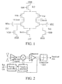
- a possible architecture for such IR-UWB receiver is shown in Figure 2.
- This architecture corresponds to a coherent receiver that decides the output data symbol after integrating the result of the multiplication of the received signal with a locally generated template waveform.
- a Low Noise Amplifier (LNA) is needed at the input, in order to adapt the antenna impedance to the input and to minimize the noise of the receiver chain by providing enough gain.
- the LNA has to add low noise by itself to the received signal.
- the received waveform has a very small duty cycle
- blocks such as the LNA, the multiplier or the integrator do not need to operate continuously, just when the pulse is received.
- the receiver chain is built fully differential in order to minimize the influence of the substrate noise coupled from the digital section of the receiver (to be integrated in the same die) as well as to reduce the undesired effects due to the coupling of the ON/OFF switching signal itself.
- IR-UWB receiver front-ends can ideally work only when a pulse is expected to arrive.
- Switching ON and OFF the LNA is a known technique that allows an important power saving. For example, assuming a received pulse of duration 1 ns, and a data rate of 100 Mps, an ideal power reduction of 90 % can be achieved if the front-end blocks are turned ON only during the pulse time. In practice the power saving will not be so high, as the LNA must be switched ON some time in advance to the reception of the pulse in order to be completely stabilized when the pulse arrives.
- FIG. 1 represents an analog circuit of a LNA with power switch described on said paper, in which the power consumption is reduced by switching the bias current, which is the advantage of the discontinuous feature of the pulse based UWB.
- the LNA of figure 1 uses a technique of switching OFF and ON one of the active devices of each branch by acting over the gate of said devices, to interrupt the flow of current between VDD and GND. This is done typically using NMOS cascode/cascade transistors because their gate can be DC powered to VDD in the ON state. Shorting it to ground in the OFF state effectively powers down the amplifier. More in detail, in the LNA of figure 1 the circuit is powered down by means of transistors (Tr1),(Tr2) connecting to ground the gates of the transistors which receive a RF input signal (RFin).
- transistors (Tr1),(Tr2) connecting to ground the gates of the transistors which receive a RF input signal (RFin).
- Transistor (Tr1),(Tr2) used to perform the on/off switching interfere with the input signal path and the input matching network and consequently negatively affect the LNA gain and linearity.
- Transistor (Tr3) is used to disconnect the whole amplifier from the power supply.
- CCC Capacitive Cross-Coupling
- the present invention provides a Low Noise Amplifier LNA for UWB systems and more preferably for coherent IR-UWB receivers.
- LNA Low Noise Amplifier
- a low-power operation achieved by the simple structure of the LNA in addition to its differential output makes it a good candidate to enable low-cost, low-power and moderate data-rate single chip IR-UWB transceivers for instance for smart tags, sensor networks or body area network (BAN) communication applications.
- BAN body area network
- a first aspect of the invention refers to a low noise amplifier LNA which comprises at least first and second amplifying elements coupled to cooperate in amplifying an input signal, so that the first amplifying element has an input node to receive said input signal, and wherein switching means are coupled to the second amplifying element to switch on and off the whole LNA by switching on and off said second amplifying element together with the rest of LNA configuring elements. Therefore, the LNA is switched on and off only by switching on and off the amplifying element that does not receive the input signal.
- An output terminal of the first amplifying stage or element is coupled to an input terminal of the second amplifying element, so that a signal amplified by the first amplifying element is subsequently amplified by the second amplifying element.
- An output node of the amplifier is coupled to the second amplifying element.
- the on/off switching is applied only to the second amplifying stage, so that the switching means do not interfere with the input matching network of the first amplifying stage.
- Another aspect of the invention refers to a method of amplifying a radio frequency signal using active and passive devices with a configuration that provides low noise amplification.
- the method comprises the reception of a radio frequency signal pulse frame and inputting the received signal to an amplification element, and switching ON the amplifier only during a time window substantially similar to the duration of said pulse frame, characterised in that the signal pulse frame is applied to a first amplifying element, and the amplifier is switched on and off by acting on a second amplifying element coupled to said first amplifying element.
- an output signal from the first amplifying element is applied as input signal to the second amplifying element, so that both amplifying elements cooperate in amplifying said signal-
- the first amplifying element preferably is a common gate transistor and the second amplifying element is a common source transistor, and the signal at the drain of the common gate transistor is applied to the gate of the common source transistor.
- the common source transistor is switched on and off by acting on the bias applied to its gate terminal.
- the first amplifying element is a common source transistor and the second amplifying element is a common gate transistor coupled in a cascode configuration.
- the amplifier is switched on and off by acting on the bias applied to the gate terminal of the common gate transistor.
- narrowband interferences can be the most limiting factor in IR-UWB systems.
- An architectural solution commonly adopted is to filter the interferences in reception as much as possible (for example, interferences due to wireless systems operating in the 2.4 and 5 GHz ISM bands). Such filtering implies losing some of the energy of the pulse around the interferences frequencies.
- a central frequency of 8 GHz has been adopted for the amplifier, and a limited -3 dB bandwidth of 1 GHz, avoiding the crowded 2.4 GHz and 5 GHz bands.
- two LNAs have been designed in the present invention having a resonant behaviour. Although it could seem surprising in a UWB application, the resulting pass band obtained is wide enough to receive correctly a pulse whose energy is centered around 8 GHz.
- the most important characteristics typically required for a LNA are low noise, high gain and acceptable linearity.
- the required power consumption strongly depends on the application.
- power consumption together with gain and the mentioned central frequency, are the most important design constraints, whereas an acceptable noise figure (not the lowest possible) is enough.
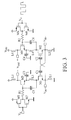
- This first LNA is composed by two symmetrical circuit branches to implement a differential amplifier, and comprises a differential Common Gate (CG) input stage composed of a first transistor (M1) and a second transistor (M2) (biasing resistors in its gates are omitted for simplicity), with first inductor (L1) and second inductor (L2) connected respectively between the source of the first and second common gate transistors (M1,M2) and ground, to choke the signal path to ground.
- CG Common Gate
- Such a CG input allows the use of the Capacitive Cross Coupling (CCC) technique by means of first capacitor (C1) and second capacitor (C2), which basically improves the CG stage gain.
- CCC Capacitive Cross Coupling
- a first coupling capacitor (C1) is connected between the gate of the first common gate transistor (M1) and the source of the second common gate transistor (M2), and a second coupling capacitor (C2) is connected between the gate of (M2) and the source of (M1).
- a Cross Coupling scheme can be implemented without the use of coupling capacitors, in which case the gate of transistor (M1) is connected directly to the source of transistor (M2), and the gate of transistor (M2) is connected directly to the source of transistor (M1).
- a common source (CS) stage is provided for the first and second differential branches of the circuit.
- This CS stage is composed by a third transistor arranged as a first common source transistor (M3) for a first circuit branch, and a fourth transistor arranged as a second common source transistor (M4) for a second circuit branch.
- M3 first common source transistor
- M4 second common source transistor
- the drains of the common gate transistors (M1,M2) are respectively coupled to the gates of the common source transistors (M3, M4), through a first impedance, the value of said first impedance being selected at least in part to couple a signal at the drain of the common gate transistors (M1,M2) to the gates of the common source transistors (M3,M4).
- Said impedances are preferably a fifth coupling capacitor (C5) for transistors (M1,M3) and a sixth coupling capacitor (C6) for transistors (M2,M4), as shown in figure 3.
- a second impedance is connected between the sources of the common source transistors (M3,M4) and the drains of the common gate transistor (M1,M2), the value of said second impedance being selected at least in part to prevent a signal at the drain of the common gate transistor (M1,M2) from entering into the common source transistor (M3,M4).
- Said second impedance consist preferably in a third choke inductor (L3) for transistors (Ml,M3) and a fourth choke inductor (L4) for transistors (M2,M4).
- Bypass third and fourth capacitors (C3) and (C4) are respectively connected between the source of the transistors (M3,M4) and ground. Choke inductors (L3,L4) and capacitors (C3,C4) prevent said AC signal from entering into the CS stage through the sources.
- the switching means are coupled to the gate of the common source transistors (M3,M4) through an impedance, preferably through resistors (R1,R2) which value is selected to at least in part to prevent a signal at the gate of the common source transistors (M3,M4), from entering into the switching means.
- the drain of the common source transistors (M3,M4) are coupled to the DC power supply through an impedance, preferably though a through a fifth choke inductor (L5) and a sixth choke inductor (L6) respectively.
- Input nodes (Vin+) and (Vin-) are respectively coupled to the source terminal of the first and second common gate transistors (M1,M2), and output nodes (Vout+) and (Vout-) are respectively coupled to the drain terminals of the first and second common source transistors (M3,M4),
- the LNA of figure 3 can be implemented without a CCC scheme, in which case the input nodes (Vin+) and (Vin-) are connected to the gate terminals of the first and second transistors (M1,M2), in which case these transistors will be arranged as common source transistors.
- the LNA of figure 3 can alternatively be implemented with a single circuit branch comprising only the transistors (M2) and (M4), or only the transistors (M1) and (M3), and the associated impedances as previously described and shown in the left (first) and right (second) circuit branches of figure 3, in which case obviously the cross-coupling scheme could not be used.
- the design is optimized for power consumption and gain, not for noise neither for linearity.
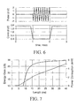
- the power gain ( S21 ) of the LNA of figure 3 is shown, where it can be observed that a gain of about 18 dB is obtained at 8 GHz, together with a -3 dB bandwidth of about 1 GHz.
- the attenuation provided at 2.4 GHz is 73 dB with respect to the central frequency, and 36.7 dB at 5 GHz.
- the distortion that the LNA causes into the pulse shape due to its limited bandwidth has been proved not to affect the overall system performance.
- the noise figure is also plotted. A value around 4 dB is obtained in the band of interest. As it can be seen, good input matching is also achieved.
- the DC power consumption obtained for continuous operation of this example is 4.87 mW
- the second LNA topology designed in the present invention is shown. It is a differential common source cascoded LNA, with choke seventh and eighth inductors (L7) and (L8) as loads.
- a ninth transistor is arranged as a third common source transistor (M9), and an eleventh transistor is arranged as third common gate transistor (M11).
- the source of the common gate transistor (M11) is connected to the drain of common source transistor (M9) so that both transistors are coupled in a cascode configuration to cooperate in a known manner in amplifying an input signal.
- a tenth transistor is arranged as a fourth common source transistor (M10), and a twelfth transistor is arranged as fourth common gate transistor (M12).
- the source of the common gate transistor (M12) is connected to the drain of common source transistor (M10) so that both transistors are coupled in a cascade configuration.
- Biasing resistors of transistors (M9 - M12) are omitted for simplicity.
- the switching means are connected directly to the gate terminal of the common source transistors (M11, M12).
- Input ports (Vin+) and (Vin-) are respectively coupled to the gate of the common source transistors (M9,MIO), and output ports (Vout+) and (Vout-) are respectively coupled to the drains terminals of the common gate transistors (M12,M11) .
- the input ports (Vin+) and (Vin-) are preferably coupled to the gate of the common source transistors (M9,M10), respectively through ninth and tenth inductive impedances (L9,L10), which are selected at least in part to match the input impedance (no source degeneration is used in order to maximize gain).
- the drains of the common gate transistor (M11, M12) are coupled to the DC power supply, respectively through choke inductors (L7,L8).
- the LNA of figure 3 can alternatively be implemented with a single circuit branch comprising only transistors (M9) and (M11) or only transistors (M10) and (M12), and the associated impedances as previously described and shown in the left and right symmetric circuit branches of figure 4.
- the gate of the cascoded transistors (M11) and (M12) can be switched ON/OFF very fast, as they do not belong to the signal path (that is, no choke resistor is needed), and no special voltage must be used at the gate: when the gate is connected to ground it powers down the LNA and when it is connected to VDD it powers it up.
- Figure 9 shows the power consumption and gain curves for this second LNA when the ON/OFF technique is used, for the same input signal and range of ON times used in the previous section.
- a similar behaviour in terms of power saving is observed, but it achieves a much better performance in terms of gain when an aggressive duty cycle is applied to the LNA: for example, only 1 dB of gain is lost with respect to the maximum gain when a ON time of only 2 ns is used, what allows a power consumption cut down to only 0.4 mW.
- the usual way of switching OFF and ON an analog block is by acting over the gate of one of the active devices, that is the amplifying elements or transistors, of each circuit differential branch, to interrupt the flow of current between VDD and GND.
- This is done typically in NMOS cascode/cascade transistors because their gate can be DC powered to VDD in the ON state. Shorting it to ground in the OFF state effectively powers down the amplifier.
- the LNA shown in figure 3 is powered down by switching off transistors (M3) and (M4), that is, the transistors which do not receive the input signal.
- the switching means comprises a pair of complementary transistors arranged to operate as a switch. More in particular, the switching means comprise a pMOS fifth and sixth transistors (M5,M6), and nMOS seventh and eighth transistors (M7,M8). The drains of said transistors are coupled together, and the gates of said transistors are connected together to a control node (Vc). The sources of the pMOS transistors (M5, M6) are connected to the DC power supply, and the sources of the nMOS transistors (M7,M8) are connected to ground.
- M5,M6 pMOS fifth and sixth transistors
- M7,M8 nMOS seventh and eighth transistors
- the drains of transistors (M6,M8) are coupled to the gate of transistor (M4) through a second resistor (R2), and the drains of transistors (M5,M7) are coupled to the gate of transistor (M3) through a first resistor (R1).
- drains of pairs of transistors (M6,M8), (M5,M7) are respectively connected directly to the gate of transistors (M12) and (M11),
- the switching means are operable by a square signal generated in a known manner, which is applied to the control node (Vc).
- Vc control node
- the transistors (M5) and (M6) are turned off and the transistors (M7) and (M8) are activated, and consequently the gates of transistors (M3) and (M4) are connected to ground so that transistors (M3), (M4) are switched off.
- transistors (M5) and (M6) are activated and transistors (M7),(M8) are turned off, for that the gates of transistors (M3) and (M4) are coupled to the power supply VDD and are thereby switched on.
- the switching means provide a double function, which are to activate or switch off the transistors (M3), (M4) for the LNA of figure 3.
- the switching means applied to the LNA of figure 4 operate in the same manner.
- the power consumption in continuous operation is 5.1 mW (it is slightly larger than 4.87 mW due to the power overhead of the switching circuitry).
- the power consumption curve of figure 7 clearly shows the power reduction obtained by applying the switching technique. For example, power consumption is reduced to 0.2 mW for a window length (ON time) of 5 ns. Nevertheless, due to the choke resistors (R1), (R2) needed after the buffers which control the switching of the CS transistors, the switching is slow, and the ON time must be much larger than the pulse duration in order to have some gain.
- the gain curve of figure 7 indicates that in order to avoid a gain reduction from the maximum less than -3dB, the ON time must be larger than 15 ns, what implies that the power consumption is reduced only in 3 mW, less than expected.
- the LNA of figure 4 improve the effectiveness of the switching technique in terms of power saving for high data rates.
- F ⁇ O ⁇ M Energy Gain Dissipated Power , where both parameters, Energy Gain (defined as equation (1)) and Dissipater Power, are in linear scale. In figure 11 this normalized FOM is plotted for different input pulse and window length.
- the CS cascoded LNA is suitable for short pulses (around few ns) and the CG-CCC cascaded LNA for longer pulses (more than 10 ns).
- the CS cascoded LNA behaves better than the CG-CCC cascaded LNA, due to its greater power consumption saving, achieved through the ON/OFF switching technique.
- Such flat zone means that, considering our figure of merit, the performance of the LNA is almost constant below 15 ns, that is, by using a shorter ON window we save power, at the price of losing gain.
- the performance of the LNA is almost constant below 15 ns, that is, by using a shorter ON window we save power, at the price of losing gain.
- the normalized figure of merit of the CG CCC cascaded LNA we can see that in the case of a longer pulse such LNA obtains a higher performance for windows lengths greater than 10 ns, and it keeps increasing as the receiving window widens until about 32 ns (when it starts to decrease). This is due to the slowness of this LNA to respond to the switching, which needs about 15 ns more than the length of the pulse to respond perfectly to it.
- the CS cascoded LNA of figure 4 which uses efficiently a fast ON/OFF switching, can be compared with the only LNA that also use this technique, obtaining that our implementation consumes less: although in Table I a consumption of 0.22 mW@25 Mpps is given since this is the data directly obtained from the plotted curves, is possible to directly extrapolate this figure to 0.44m W@50 Mpps, a 34 % less than Reference [8].
- Table I Comparison of Different Implementations: Ref Technology Topology BW (GHz) Gain (dB) S11 (dB) NF (dB) Pdiss 4 (mW) Pdiss (mW) ON/OFF (7) 0 18 ⁇ m CMOS CS.
- the first LNA presented (figure 3), which uses a common gate capacitive-cross-coupling (CG-CCC) cascaded structure, has better performances for the same DC power consumption (basically in terms of gain) than the second LNA (figure 4), which uses a typical common source (CS) cascoded structure.
- CG-CCC common gate capacitive-cross-coupling
- CS common source
- the CG CCC LNA fails to keep a fast switching (that is, for high data-rates), while the CS cascoded LNA behaves much better in such situation.
- the first LNA has good performances when the received pulses duration is in the order of 10 ns length, while the second one has its best performances when the pulse is in the order of few ns of length.
- the CS cascoded LNA can be used to efficiently trade-off gain per dissipated power when the received pulse is long,
- the CG CCC Cascaded LNA of the invention behaves very well, having the highest Gain/Power ratio. If it is ON/OFF switched, it can improve its consumption, although particularly for moderate data rates.
- the CS Cascoded LNA of the invention compared to the only LNA that is ON/OFF switched, behaves a 34 % better, achieving 0.44 mW@50 Mpps.
- the invention also refers to an impulse-radio receiver coupled to an antenna for receiving radio signals, having the previously described low noise amplifier for amplifying signals received by said antenna.
- the antenna can be for example a differential antenna.
- the invention also refers to an integrated circuit having the previously described low noise amplifier, in its semiconductor die.
- the invention also refers to a wireless communication device including the previously described low noise amplifier.
Abstract

Description
- The present invention is related to low power low noise amplifiers (LNA) including on/off switching capability, which are preferably used in impulse radio (IR) ultra-wideband (UWB) receivers.
- In the invention a very low power and high-gain common gate amplifier is proposed. This first LNA provides an optimum gain for large ON times, so that the best effectiveness of this topology is obtained when the pulse length is long enough (in the range of several ns).
- The invention provides also a second LNA for shorter received pulse widths, with the aim of implementing a fast enough ON/OFF switching.
- When the LNAs are operated continuously (i.e., infinite ON time) the second LNA has a lower gain for the same power consumption than the first one. However, if the ON/OFF switching technique is applied, the second topology achieves higher gain for shorter ON times, which implies that it is best suited for higher data rates.
- The invention is also related to a method of amplifying a radio frequency signal using a plurality of active and passive devices with a configuration that provides low noise amplification.
- Since the publication of the paper: FFC, "First Report and Order: Revision of , by the United States Federal Communications Commission (FCC), Ultra-Wideband (UWB) communication techniques have received increasing attention for short-range, high-data rate wireless communication applications. Impulse Radio (IR) implementation of such UWB systems has become a very interesting candidate due to its low complexity, low power consumption, low cost, high data rate and the ability of coexistence with other radio systems.
- In its usual realization, an IR-UWB transmitter consists on a pulse generator that is triggered regularly by a timing circuitry, that is the IR-UWB is based on the transmission and reception of very short pulses at a certain periodicity. The output of the pulse generator is connected directly to the antenna. No Power Amplifier is needed since the UWB transmitted power is very low. Data is transmitted by modifying some parameter of the pulse (for example, its sign in BPSK modulation or its position in PPM modulation). The transmitted output waveform has a very small duty cycle since the sub-nanosecond pulses are sent every frame, which for usual data rates has a duration of several nanosecond.
- Time Hoping (TH) technique is commonly used to allow multiple users access and to avoid peaks in the spectrum of the UWB signal. A pseudorandom code locates each successive pulse in a different position along its frame. The IR-UWB receiver can be implemented in several ways, but the present invention is focused on a very low-power implementation for short distances (less than 1 meter for Body Area Network, BAN, applications). A possible architecture for such IR-UWB receiver is shown in Figure 2.
- This architecture corresponds to a coherent receiver that decides the output data symbol after integrating the result of the multiplication of the received signal with a locally generated template waveform. A Low Noise Amplifier (LNA) is needed at the input, in order to adapt the antenna impedance to the input and to minimize the noise of the receiver chain by providing enough gain. The LNA has to add low noise by itself to the received signal.
- As the received waveform has a very small duty cycle, blocks such as the LNA, the multiplier or the integrator do not need to operate continuously, just when the pulse is received. By applying a clever ON/OFF switching on these blocks an important saving of power consumption can be obtained. Additionally, the receiver chain is built fully differential in order to minimize the influence of the substrate noise coupled from the digital section of the receiver (to be integrated in the same die) as well as to reduce the undesired effects due to the coupling of the ON/OFF switching signal itself.
- As in other systems that work in burst mode, IR-UWB receiver front-ends can ideally work only when a pulse is expected to arrive. Switching ON and OFF the LNA is a known technique that allows an important power saving. For example, assuming a received pulse of
duration 1 ns, and a data rate of 100 Mps, an ideal power reduction of 90 % can be achieved if the front-end blocks are turned ON only during the pulse time. In practice the power saving will not be so high, as the LNA must be switched ON some time in advance to the reception of the pulse in order to be completely stabilized when the pulse arrives. - A LNA with power switch is described in the technical paper entitled " Transceivers circuits for pulse-based ultra-wideband" in the IEEE Journal 0-7803-8251-X/2004 IEEE. Figure 1 represents an analog circuit of a LNA with power switch described on said paper, in which the power consumption is reduced by switching the bias current, which is the advantage of the discontinuous feature of the pulse based UWB.
- The LNA of figure 1 uses a technique of switching OFF and ON one of the active devices of each branch by acting over the gate of said devices, to interrupt the flow of current between VDD and GND. This is done typically using NMOS cascode/cascade transistors because their gate can be DC powered to VDD in the ON state. Shorting it to ground in the OFF state effectively powers down the amplifier. More in detail, in the LNA of figure 1 the circuit is powered down by means of transistors (Tr1),(Tr2) connecting to ground the gates of the transistors which receive a RF input signal (RFin). In that switching scheme, the transistors (Tr1),(Tr2) used to perform the on/off switching, interfere with the input signal path and the input matching network and consequently negatively affect the LNA gain and linearity. Transistor (Tr3) is used to disconnect the whole amplifier from the power supply.
- On the other hand, a Capacitive Cross-Coupling (CCC) technique is known to improve the performance of a differential amplifying stage. More details of this CCC technique can be found on the papers: "Wei Zhou, Sherif Embabi, José Pineda de Gyvez and Edgar Sánchez Sinencio, "Using Capacitive Cross-Coupling Technique in RF Low Noise Amplifiers and Down-Conversion Mixer Design", in the Proceedings of the European solid-State Circuits Conference (ESSCIRC), 19-21 Sept. 2000 Page(s):77-80", and "David J. Allstot, Xiaoyong Li, and Sudip Shekhar, "Design Considerations for CMOS Low-Noise Amplifiers", in IEEE Radio Frequency Integrated Circuits Symposium (RFIC), 2004, pp. 97-100 ".
- The present invention provides a Low Noise Amplifier LNA for UWB systems and more preferably for coherent IR-UWB receivers. A low-power operation achieved by the simple structure of the LNA in addition to its differential output makes it a good candidate to enable low-cost, low-power and moderate data-rate single chip IR-UWB transceivers for instance for smart tags, sensor networks or body area network (BAN) communication applications.
- A first aspect of the invention refers to a low noise amplifier LNA which comprises at least first and second amplifying elements coupled to cooperate in amplifying an input signal, so that the first amplifying element has an input node to receive said input signal, and wherein switching means are coupled to the second amplifying element to switch on and off the whole LNA by switching on and off said second amplifying element together with the rest of LNA configuring elements. Therefore, the LNA is switched on and off only by switching on and off the amplifying element that does not receive the input signal.
- An output terminal of the first amplifying stage or element is coupled to an input terminal of the second amplifying element, so that a signal amplified by the first amplifying element is subsequently amplified by the second amplifying element. An output node of the amplifier is coupled to the second amplifying element.
- In the present invention, while the input signal to be amplified is applied to the first amplifying stage, the on/off switching is applied only to the second amplifying stage, so that the switching means do not interfere with the input matching network of the first amplifying stage.
- Another aspect of the invention refers to a method of amplifying a radio frequency signal using active and passive devices with a configuration that provides low noise amplification. The method comprises the reception of a radio frequency signal pulse frame and inputting the received signal to an amplification element, and switching ON the amplifier only during a time window substantially similar to the duration of said pulse frame, characterised in that the signal pulse frame is applied to a first amplifying element, and the amplifier is switched on and off by acting on a second amplifying element coupled to said first amplifying element.
- In the method of the invention, an output signal from the first amplifying element is applied as input signal to the second amplifying element, so that both amplifying elements cooperate in amplifying said signal- The first amplifying element preferably is a common gate transistor and the second amplifying element is a common source transistor, and the signal at the drain of the common gate transistor is applied to the gate of the common source transistor. The common source transistor is switched on and off by acting on the bias applied to its gate terminal.
- Alternatively, the first amplifying element is a common source transistor and the second amplifying element is a common gate transistor coupled in a cascode configuration. The amplifier is switched on and off by acting on the bias applied to the gate terminal of the common gate transistor.
- The features of the invention will be better understood by reference to the accompanying drawings, which illustrate preferred embodiments of the invention.
- Figure 1.- shows a prior-art LNA topology including on-off switching capability.
- Figure 2.- shows a block diagram of an architecture for an impulse-radio receiver.
- Figure 3.- shows a preferred embodiment of a Common Gate Capacitive Cross Coupling Cascaded LNA.
- Figure 4,- shows a preferred embodiment of a Common Source Cascoded LNA.
- Figure 5.- shows a diagram of the power gain S21 (solid line, left axis) and Noise Figure NF (doted line, left axis) and reflection coefficient S11 (dashed line, right axis) of the CG-CCC LNA of figure 3.
- Figure 6.- shows a diagram of an example of a sinusoidal pulse frame used as input (top) and a diagram of the control voltage Vc (bottom).
- Figure 7.- shows a diagram of the energy gain (solid line, left axis) and dissipated power (dashed line, right axis) versus window/pulse length, for the CG CCC cascaded LNA of figure 3.
- Figure 8.- shows a diagram of the power gain S21 (solid line, left axis) and NF (doted line, left axis) and reflection coefficient S11 (dashed line, right axis) of the CS cascoded LNA, of figure 4.
- Figure 9.- shows a diagram of the energy gain (solid line, left axis) and dissipated power (dashed line, right axis) versus window/pulse length, for the CS cascoded LNA of figure 4.
- Figure 10. - shows a diagram of the energy Gain versus window/pulse length, for the CG CCC cascaded LNA (solid line) of figure 3 and for the CS cascoded LNA (dashed line) of figure 4.
- Figure 11.- shows a diagram of the Normalized Fig. of Merit for the CG CCC cascaded LNA (solid line) and for the CS cascoded LNA (dashed line).
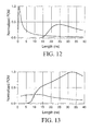
- Figure 12.- shows a diagram of the Normalized Fig. of Merit for the CG CCC cascaded LNA (solid line) and for the CS cascoded LNA (dashed line), when a pulse of a fixed length of 750 ps is received, for different receiving windows lengths.
- Figure 13.- shows a diagram of the Normalized Fig. of Merit for the CG CCC cascaded LNA (solid line) and for the CS cascaded LNA (dashed line), when a pulse of a fixed length of 15 ns is received, for different receiving windows lengths.
- It is well known that narrowband interferences can be the most limiting factor in IR-UWB systems. An architectural solution commonly adopted is to filter the interferences in reception as much as possible (for example, interferences due to wireless systems operating in the 2.4 and 5 GHz ISM bands). Such filtering implies losing some of the energy of the pulse around the interferences frequencies.
- In a preferred embodiment of the invention, a central frequency of 8 GHz has been adopted for the amplifier, and a limited -3 dB bandwidth of 1 GHz, avoiding the crowded 2.4 GHz and 5 GHz bands. To attenuate the effect of the above mentioned interferences, two LNAs have been designed in the present invention having a resonant behaviour. Although it could seem surprising in a UWB application, the resulting pass band obtained is wide enough to receive correctly a pulse whose energy is centered around 8 GHz.
- The most important characteristics typically required for a LNA are low noise, high gain and acceptable linearity. The required power consumption strongly depends on the application. In the present invention where the communication systems are preferably integrated in sensor networks or BAN devices with energy harvesting techniques, power consumption, together with gain and the mentioned central frequency, are the most important design constraints, whereas an acceptable noise figure (not the lowest possible) is enough.
- Having all these issues in mind, a first preferred design of a LNA according to the invention has been represented in figure 3. This first LNA is composed by two symmetrical circuit branches to implement a differential amplifier, and comprises a differential Common Gate (CG) input stage composed of a first transistor (M1) and a second transistor (M2) (biasing resistors in its gates are omitted for simplicity), with first inductor (L1) and second inductor (L2) connected respectively between the source of the first and second common gate transistors (M1,M2) and ground, to choke the signal path to ground.
- Such a CG input allows the use of the Capacitive Cross Coupling (CCC) technique by means of first capacitor (C1) and second capacitor (C2), which basically improves the CG stage gain.
- More in detail, a first coupling capacitor (C1) is connected between the gate of the first common gate transistor (M1) and the source of the second common gate transistor (M2), and a second coupling capacitor (C2) is connected between the gate of (M2) and the source of (M1). Alternatively, a Cross Coupling scheme can be implemented without the use of coupling capacitors, in which case the gate of transistor (M1) is connected directly to the source of transistor (M2), and the gate of transistor (M2) is connected directly to the source of transistor (M1).
- On top of the CG stage, a common source (CS) stage is provided for the first and second differential branches of the circuit. This CS stage is composed by a third transistor arranged as a first common source transistor (M3) for a first circuit branch, and a fourth transistor arranged as a second common source transistor (M4) for a second circuit branch. The CS stage reuses the same DC current of the CG input stage as an efficient power consumption saving technique.
- The drains of the common gate transistors (M1,M2) are respectively coupled to the gates of the common source transistors (M3, M4), through a first impedance, the value of said first impedance being selected at least in part to couple a signal at the drain of the common gate transistors (M1,M2) to the gates of the common source transistors (M3,M4). In this arrangement an AC signal is applied from the CG stage to the CS stage, so that both transistors are cooperating in amplifying an input signal in a cascaded configuration. Said impedances are preferably a fifth coupling capacitor (C5) for transistors (M1,M3) and a sixth coupling capacitor (C6) for transistors (M2,M4), as shown in figure 3.
- Furthermore, a second impedance is connected between the sources of the common source transistors (M3,M4) and the drains of the common gate transistor (M1,M2), the value of said second impedance being selected at least in part to prevent a signal at the drain of the common gate transistor (M1,M2) from entering into the common source transistor (M3,M4). Said second impedance consist preferably in a third choke inductor (L3) for transistors (Ml,M3) and a fourth choke inductor (L4) for transistors (M2,M4).
- Bypass third and fourth capacitors (C3) and (C4) are respectively connected between the source of the transistors (M3,M4) and ground. Choke inductors (L3,L4) and capacitors (C3,C4) prevent said AC signal from entering into the CS stage through the sources.
- The switching means are coupled to the gate of the common source transistors (M3,M4) through an impedance, preferably through resistors (R1,R2) which value is selected to at least in part to prevent a signal at the gate of the common source transistors (M3,M4), from entering into the switching means.
- As it can be seen in figure 3, the drain of the common source transistors (M3,M4) are coupled to the DC power supply through an impedance, preferably though a through a fifth choke inductor (L5) and a sixth choke inductor (L6) respectively.
- Input nodes (Vin+) and (Vin-) are respectively coupled to the source terminal of the first and second common gate transistors (M1,M2), and output nodes (Vout+) and (Vout-) are respectively coupled to the drain terminals of the first and second common source transistors (M3,M4),
- Alternatively the LNA of figure 3, can be implemented without a CCC scheme, in which case the input nodes (Vin+) and (Vin-) are connected to the gate terminals of the first and second transistors (M1,M2), in which case these transistors will be arranged as common source transistors.
- Also, in another preferred embodiment of the invention, the LNA of figure 3, can alternatively be implemented with a single circuit branch comprising only the transistors (M2) and (M4), or only the transistors (M1) and (M3), and the associated impedances as previously described and shown in the left (first) and right (second) circuit branches of figure 3, in which case obviously the cross-coupling scheme could not be used.
- The design is optimized for power consumption and gain, not for noise neither for linearity. In figure 5 the power gain (S21) of the LNA of figure 3 is shown, where it can be observed that a gain of about 18 dB is obtained at 8 GHz, together with a -3 dB bandwidth of about 1 GHz. The attenuation provided at 2.4 GHz is 73 dB with respect to the central frequency, and 36.7 dB at 5 GHz. The distortion that the LNA causes into the pulse shape due to its limited bandwidth has been proved not to affect the overall system performance. In the same figure 5 the noise figure is also plotted. A value around 4 dB is obtained in the band of interest. As it can be seen, good input matching is also achieved. Finally, the DC power consumption obtained for continuous operation of this example is 4.87 mW,
- In figure 4 the second LNA topology designed in the present invention is shown. It is a differential common source cascoded LNA, with choke seventh and eighth inductors (L7) and (L8) as loads.
- In the left branch of the circuit of figure 4, a ninth transistor is arranged as a third common source transistor (M9), and an eleventh transistor is arranged as third common gate transistor (M11). The source of the common gate transistor (M11) is connected to the drain of common source transistor (M9) so that both transistors are coupled in a cascode configuration to cooperate in a known manner in amplifying an input signal.
- Similarly in the right branch of this circuit, a tenth transistor is arranged as a fourth common source transistor (M10), and a twelfth transistor is arranged as fourth common gate transistor (M12). The source of the common gate transistor (M12) is connected to the drain of common source transistor (M10) so that both transistors are coupled in a cascade configuration. Biasing resistors of transistors (M9 - M12) are omitted for simplicity.
In this embodiment, the switching means are connected directly to the gate terminal of the common source transistors (M11, M12). - Input ports (Vin+) and (Vin-) are respectively coupled to the gate of the common source transistors (M9,MIO), and output ports (Vout+) and (Vout-) are respectively coupled to the drains terminals of the common gate transistors (M12,M11) .
- The input ports (Vin+) and (Vin-) are preferably coupled to the gate of the common source transistors (M9,M10), respectively through ninth and tenth inductive impedances (L9,L10), which are selected at least in part to match the input impedance (no source degeneration is used in order to maximize gain).
- The drains of the common gate transistor (M11, M12) are coupled to the DC power supply, respectively through choke inductors (L7,L8).
- In another preferred embodiment of the invention, the LNA of figure 3, can alternatively be implemented with a single circuit branch comprising only transistors (M9) and (M11) or only transistors (M10) and (M12), and the associated impedances as previously described and shown in the left and right symmetric circuit branches of figure 4.
- With this structure, the gate of the cascoded transistors (M11) and (M12) can be switched ON/OFF very fast, as they do not belong to the signal path (that is, no choke resistor is needed), and no special voltage must be used at the gate: when the gate is connected to ground it powers down the LNA and when it is connected to VDD it powers it up.
- In figure 8 the power gain (S21 parameter), noise figure, and reflection coefficient (S11 parameter) are shown. In order to make fair comparisons, this second LNA has been designed to consume the same continuous-operation DC power than the previous one (4.87 mW). We observe that the gain is 8 dB lower than in the previous LNA, noise figure is about 0.5 dB higher, and the input matching is, although acceptable, slightly worse. The attenuation (relative to the peak gain) provided at 2.4 GHz is 42.3 dB, and 24.7 dB at 5 GHz. That is, for the same power consumption, performances are lower than in the first LNA of figure 3.
- The advantage of this alternative topology is its capability for using a fast ON/OFF switching technique with great performances. Figure 9 shows the power consumption and gain curves for this second LNA when the ON/OFF technique is used, for the same input signal and range of ON times used in the previous section. A similar behaviour in terms of power saving is observed, but it achieves a much better performance in terms of gain when an aggressive duty cycle is applied to the LNA: for example, only 1 dB of gain is lost with respect to the maximum gain when a ON time of only 2 ns is used, what allows a power consumption cut down to only 0.4 mW.
- The usual way of switching OFF and ON an analog block is by acting over the gate of one of the active devices, that is the amplifying elements or transistors, of each circuit differential branch, to interrupt the flow of current between VDD and GND. This is done typically in NMOS cascode/cascade transistors because their gate can be DC powered to VDD in the ON state. Shorting it to ground in the OFF state effectively powers down the amplifier. For example, the LNA shown in figure 3 is powered down by switching off transistors (M3) and (M4), that is, the transistors which do not receive the input signal.
- In the present invention it has been considered that some of the key issues when applying this technique to high frequency amplifiers are: first, as the central frequency is so high, the devices used to perform the ON/OFF switching must not interfere with the signal path since it would affect the LNA gain; second, when the data rate is high, the block must respond very fast to the switching in order to be energetically efficient. In order words, the gate of the transistor to be controlled must be a low impedance node, otherwise the switching will not be fast enough, the ON time would have to be increased, and consequently, less power will be saved.
- In the LNA of figure 3, all the gates of the LNA transistors carry signal (the gates of the CG stage are used for the cross-coupling technique, and the gates of the CS states are connected to the output signal of the previous CG stage). This complicates the implementation of the ON/OFF switching, but a satisfactory result have been obtained by controlling the gate of the cascaded CS stage (see in figure 3 the buffers made of transistors M5-M7 and M6-M8). Choke resistors (R1) and (R2) are connected between the buffers and the CS gates to minimize the losses of the LNA gain, since signal passes through this node. In order to optimally size these resistors, a trade-off must be made between fast response of the LNA to the control signal (Vc) (low values of R1, R2) and low loss of LNA gain (high values of R1 R2).
- In a preferred embodiment of the invention, the switching means comprises a pair of complementary transistors arranged to operate as a switch. More in particular, the switching means comprise a pMOS fifth and sixth transistors (M5,M6), and nMOS seventh and eighth transistors (M7,M8). The drains of said transistors are coupled together, and the gates of said transistors are connected together to a control node (Vc). The sources of the pMOS transistors (M5, M6) are connected to the DC power supply, and the sources of the nMOS transistors (M7,M8) are connected to ground.
- In the case of the LNA of figure 3, the drains of transistors (M6,M8) are coupled to the gate of transistor (M4) through a second resistor (R2), and the drains of transistors (M5,M7) are coupled to the gate of transistor (M3) through a first resistor (R1).
- In the case of the LNA of figure 4, the drains of pairs of transistors (M6,M8), (M5,M7) are respectively connected directly to the gate of transistors (M12) and (M11),
- For both LNA s described, the switching means are operable by a square signal generated in a known manner, which is applied to the control node (Vc). Taking as example the LNA of figure 3, in the positive voltage values of said square signal (Vc=Vdd), the transistors (M5) and (M6) are turned off and the transistors (M7) and (M8) are activated, and consequently the gates of transistors (M3) and (M4) are connected to ground so that transistors (M3), (M4) are switched off. In the negative voltage values of said control square signal (Vc= GND), transistors (M5) and (M6) are activated and transistors (M7),(M8) are turned off, for that the gates of transistors (M3) and (M4) are coupled to the power supply VDD and are thereby switched on.
- Therefore the switching means provide a double function, which are to activate or switch off the transistors (M3), (M4) for the LNA of figure 3.
- The switching means applied to the LNA of figure 4, operate in the same manner.
- The effectiveness of the ON/OFF switching technique has been investigated by simulation using a pulse consisting of a sinusoidal burst with 8 GHz of frequency and a length of several cycles as input signal. The LNA is turned ON during a time window equal to the pulse duration (see figure 6). In figure 7 the power dissipated by the LNA is shown. The integration period considered to calculate the power is the maximum window length used, i,e. 40 ns. In the same figure, the gain of the LNA under the switching conditions is shown, The S21 parameter can not be used as gain in such situation, due to the LNA ON/OFF behaviour, since now the gain is a large signal magnitude. Instead of S21 we can use the Energy Gain, defined as:

- Now the power consumption in continuous operation is 5.1 mW (it is slightly larger than 4.87 mW due to the power overhead of the switching circuitry). The power consumption curve of figure 7 clearly shows the power reduction obtained by applying the switching technique. For example, power consumption is reduced to 0.2 mW for a window length (ON time) of 5 ns. Nevertheless, due to the choke resistors (R1), (R2) needed after the buffers which control the switching of the CS transistors, the switching is slow, and the ON time must be much larger than the pulse duration in order to have some gain. The gain curve of figure 7 indicates that in order to avoid a gain reduction from the maximum less than -3dB, the ON time must be larger than 15 ns, what implies that the power consumption is reduced only in 3 mW, less than expected. The LNA of figure 4, improve the effectiveness of the switching technique in terms of power saving for high data rates.
- Noise Figure and adaptation do not differ very much between both LNAs, so only gain, as defined in equation (1), and power consumption are considered. In figure 10 the same curves corresponding to the energy gain of both LNAs previously obtained are plotted together. We can observe that for short pulses the CS cascoded LNA behaves much better than the other (indeed, the CG CCC cascaded LNA does not work for ON times below 5 ns). But in cases where the pulse is in the order of about 12 ns of length or more, the CG CCC cascaded LNA behaves better in terms of gain, achieving till 7 dBs more gain than the CS LNA.
- To compare both LNAs taking into account also the power consumption, the following Figure Of Merit has been defined:

where both parameters, Energy Gain (defined as equation (1)) and Dissipater Power, are in linear scale. In figure 11 this normalized FOM is plotted for different input pulse and window length. We can derive again that, by using this figure of merit, the CS cascoded LNA is suitable for short pulses (around few ns) and the CG-CCC cascaded LNA for longer pulses (more than 10 ns). We can also say that, in absolute terms, the CS cascoded LNA behaves better than the CG-CCC cascaded LNA, due to its greater power consumption saving, achieved through the ON/OFF switching technique. - Until now different pulse durations have been considered (parameter "Length" in the figures), assuming an ON time equal to the pulse duration (see figure 6). This is reasonable if we think that the best way to detect the pulse is to use all its energy. However, when power consumption is also taken into account, an interesting trade-off appears: for an arbitrary length of the received pulse it may be possible to use only part of its energy for detection, obtaining less gain but consuming less power. That is, the gain is traded-off for power consumption using the ON/OFF switching technique.
- Similar simulations have been performed but considering the length of the received pulse fixed and varying the length of the receiving window. In figure 12 we can see such a case for a short received pulse of 750 ps. Since in this case there is no possibility for trading-off energy for power consumption because of the shortness of the pulse, plots do not differ significantly from those in figure 11. When a longer received pulse of 15 ns is considered, plots in figure 13 are obtained. We can see how the CS cascoded LNA has a flat zone below 15 ns (after that point, which is the length of the pulse, the FOM decreases: obviously it makes no sense to keep the LNA working after the end of the pulse, as it increases the dissipated power without increasing the received energy).
- Such flat zone means that, considering our figure of merit, the performance of the LNA is almost constant below 15 ns, that is, by using a shorter ON window we save power, at the price of losing gain. Looking at the normalized figure of merit of the CG CCC cascaded LNA, we can see that in the case of a longer pulse such LNA obtains a higher performance for windows lengths greater than 10 ns, and it keeps increasing as the receiving window widens until about 32 ns (when it starts to decrease). This is due to the slowness of this LNA to respond to the switching, which needs about 15 ns more than the length of the pulse to respond perfectly to it.
- A comparison of the performances of both LNAs with state of the art LNAs, is presented in Table I. Although the comparison is not straightforward due to the wide variety of implementations (0.13 and 0.18 µm technologies, single and differential output, lower and upper frequency band, continuous and ON/OFF working mode), we have tried to show the whole picture of the state of the art. If we compare the CG CCC cascaded LNA of the present invention (which has high performances when working continuously) with the others it has been found that it behaves very well (indeed, it is the LNA with the highest Gain/Power figure of merit). If the ON/OFF switching is applied it saves some power, although the best performance is obtained at medium and low data-rates, i.e. for long ON times.
- The CS cascoded LNA of figure 4, which uses efficiently a fast ON/OFF switching, can be compared with the only LNA that also use this technique, obtaining that our implementation consumes less: although in Table I a consumption of 0.22 mW@25 Mpps is given since this is the data directly obtained from the plotted curves, is possible to directly extrapolate this figure to 0.44m W@50 Mpps, a 34 % less than Reference [8].
Table I: Comparison of Different Implementations: Ref Technology Topology BW (GHz) Gain (dB) S11 (dB) NF (dB) Pdiss4 (mW) Pdiss (mW) ON/OFF (7) 0 18 µm CMOS CS. cascoded, single ended 2.3.9.2 9 3 <-9 9 4.0-7.0 9 -- (8) 0 18 µm CMOS CS, differential 0.1-1.0 18 -- 5.32 - 0 671@50Mpps (9) 0 18 µm CMOS CS, shunt-feedback, single ended 20-46 9.8 <-9 2.32 12.6 -- (10) 0.18 µm CMOS CS cascoded+SF, sing ended, tunable 6.0-10.0 116 <-9 4.753 11.6 -- (11) 0 13 µm CMOS CS cascoded, single ended 3.0-10.7 11 <-10 222 4.8 -- (12) 0 18 µm CMOS CS cascaded, single ended 26-9.2 10.9 <-11 352 7.1 - (13) 0 13 µm CMOS CG shunt feedback CCC. differential 0.1-0.93 13 <-15 42 7.2 - (14) SiGe CS shunt feedback, single ended 2.0-10-0 13 <-7 3.32 9.6 -- (15) 0 13 µm CMOS CS cascaded + CS, differential 2.0-5 2 16 <-9 4.7-5.7 380 -- (16) 013µm CMOS CS cascaded + CS, differential 2.0-46 95 95 <-10 3.52 16.5 -- LNA fig 3 0 18 µm CMOS CG CCC Cascaded, differential 77-84 19 <-13 4.02 4.87 022@25Mpps LNA fig 4 0 18 µm CMOS CS Cascoded, differential 74-8.6 11 <-6 4.52 4.87 28@25Mpps 1CS: common source, CG: common gate, SF: source follower, CCC: Capacitive Cross Coupled.
2Minimum value in the band
3Average
4Pdiss continous - The first LNA presented (figure 3), which uses a common gate capacitive-cross-coupling (CG-CCC) cascaded structure, has better performances for the same DC power consumption (basically in terms of gain) than the second LNA (figure 4), which uses a typical common source (CS) cascoded structure. Both LNAs have been designed in a 0.18 µm CMOS process with RF options.
- However, when the ON/OFF switching is also considered, the CG CCC LNA fails to keep a fast switching (that is, for high data-rates), while the CS cascoded LNA behaves much better in such situation. As a result, the first LNA has good performances when the received pulses duration is in the order of 10 ns length, while the second one has its best performances when the pulse is in the order of few ns of length. Additionally, the CS cascoded LNA can be used to efficiently trade-off gain per dissipated power when the received pulse is long,
- Compared to state of the art LNAs operated in continuous way, the CG CCC Cascaded LNA of the invention behaves very well, having the highest Gain/Power ratio. If it is ON/OFF switched, it can improve its consumption, although particularly for moderate data rates.
- The CS Cascoded LNA of the invention, compared to the only LNA that is ON/OFF switched, behaves a 34 % better, achieving 0.44 mW@50 Mpps.
- The invention also refers to an impulse-radio receiver coupled to an antenna for receiving radio signals, having the previously described low noise amplifier for amplifying signals received by said antenna. The antenna can be for example a differential antenna.
- The invention also refers to an integrated circuit having the previously described low noise amplifier, in its semiconductor die.
- The invention also refers to a wireless communication device including the previously described low noise amplifier.
- Further embodiments of the invention are described in the attached dependent claims.
- In view of the description and set of drawings, a skilled person in the art will be able to understand that the implementations of the invention described may be combined in many ways within the purpose of the invention. The invention has been described according to some preferred embodiments of it, but for a skilled person in the art, it will be clear that many variations may be made to the preferred embodiments without departing from the object of the claimed invention.
Claims (35)
- A low noise amplifier including at least one circuit branch, a first circuit branch comprising at least first and second amplifying elements coupled to cooperate in amplifying an input signal, and switching means to switch on and off the amplifier, characterized in that the first amplifying element has an input node to receive said input signal, and wherein said switching means are only coupled to the second amplifying element to switch on and off the amplifier by acting on said second amplifying element.
- Low noise amplifier according to claim 1 wherein an output terminal of the first amplifying element is coupled to an input terminal of the second amplifying element, and an output node of the amplifier is coupled to the second amplifying element.
- Low noise amplifier according to claim 1 or claim 2 wherein the first amplifying element is a first common gate transistor (M1), and the second amplifying element is a first common source transistor (M3), and wherein the drain of the fist common gate transistor is coupled to the gate of the first common source transistor.
- Low noise amplifier according to claim 3 wherein the gate of the first common source transistor (M3) is coupled to drain of the first common gate transistor (M1) through a first impedance, the value of said first impedance being selected at least in part to couple a signal at the drain of the first common gate transistor (M1) to the gate of the first common source transistor (M3), and wherein a second impedance is connected between the source of the first common source transistor (M3) and the drain of the first common gate transistor (M1), the value of said second impedance being selected at least in part to prevent a signal at the drain of the first common gate transistor from entering into the first common source transistor (M3).
- Low noise amplifier according to claim 4 wherein the first impedance is a coupling capacitor (C5), and the second impedance is a third choke inductor (L3).
- Low noise amplifier according to any of the claims 3 to 5 wherein a bypass capacitor (C3) is connected between the source of the first common source transistor (M3) and ground.
- Low noise amplifier according to any of the claims 3 to 6 wherein a first inductive impedance (L1) is connected between the source of the first common gate transistor (M1) and ground, to choke the signal path to ground.
- Low noise amplifier according to any of the claims 3 to 7 wherein the drain of the first common source transistor (M3) is coupled to the DC power supply through a fifth choke inductor (L5,).
- Low noise amplifier according to any of the preceding claims wherein it comprises two symmetric circuit branches to form a differential amplifier, wherein a second circuit branch comprises a second common gate transistor (M2) and a second common source transistor (M4) coupled in a cascaded configuration, and wherein the first and second common gate transistors (M3.,M2) of the amplifier are provided with a differential cross-coupling input scheme to feed an input signal to the amplifier.
- Low noise amplifier according to claim 9 wherein the cross-coupling scheme comprises a series coupled capacitors (C1),(C2).
- Low noise amplifier according to claim 9 or 10 wherein a first coupling capacitor (C1) is connected between the gate of the first common gate transistor (M1) and the source of the second common gate transistor (M2), and a second coupling capacitor (C2) is connected between the gate of the second common gate transistor (M2) and the source of the first common gate transistor (M1), and wherein an input node is connected to the source of each common gate transistor (M1,M2).
- Low noise amplifier according to claim 1 or claim 2 wherein the first amplifying element is a third common source transistor (M9) and the second amplifying element is a third common gate transistor (M11), wherein the source of the common gate transistor (M11) is connected to the drain of common source transistor (M9) so that both transistors are coupled in a cascode configuration.
- Low noise amplifier according to claim 12 wherein an input port is coupled to the gate of the third common source transistor (M9), and an output port is coupled to the drain of the third common gate transistor (M11).
- Low noise amplifier according to claim 12 or 13 wherein the input port is coupled to the gate of the third common source transistor (M9) through a ninth inductive impedance (L9), which is selected at least in part to match the input impedance.
- Low noise amplifier according to any of the claims 12 to 14, wherein the drain of the third common gate transistor (M11) is coupled to the DC power supply through a seventh choke inductor (L7).
- Low noise amplifier according to any of the claims 12 to 15 wherein it comprises two symmetric circuit branches to form a differential amplifier.
- Low noise amplifier according to any of the claims 3 to 11 wherein the switching means are coupled to the gate of the common source transistors (M3,M4) through a resistor (R1,R2) selected to at least in part to prevent a signal at the gate of the common source transistors (M3,M4), from entering into the switching means.
- Low noise amplifier according to any of the claims 12 to 16 wherein the switching means are connected directly to the gate of the common source transistors (M11,M12).
- Low noise amplifier according to claim 17 or claim 18 wherein the switching means comprises a pair of complementary transistors arranged to operate as a switch.
- Low noise amplifier according to any of the claims 1, 17, 19 wherein the switching means comprise a pMOS transistor (M5,M6) and a nMOS transistor (M7,M8), and wherein the drains of said transistors are coupled together to the gate of the common source transistor (M3,M4), and the gates of said transistors are connected together to a control node (Vc), the source of the pMOS transistor (M5,M6) being connected to the DC power supply, and the source of the nMOS transistor (M7,M8) being connected to ground.
- Low noise amplifier according to any of the claims 1, 18, 19 wherein the switching means comprises a pMOS transistor (M5,M6) and a nMOS transistor (M7,M8), and wherein the drains of said transistors are connected together to the gate of the common gate transistor (M11,M12), and the gates are connected together to a control node (Vc), the source of the pMOS transistor (M5,M6) being connected to the DC power supply, and the source of the nMOS transistor (M7,M8) being connected to ground.
- Low noise amplifier according to any of the claim 17 to 21 wherein the switching means are operable by a square signal applied to the control node (Vc).
- Low noise amplifier according to any of the claims 3 to 22 wherein the transistors are implemented in CMOS technology.
- Low noise amplifier according to any of the preceding claims wherein it is adapted to operate in an Impulse-radio ultra wide band system IR-UWB.
- Low noise amplifier according to any of the preceding claims wherein it is adapted to operate within a band having a central frequency of approximately 8 Ghz.
- Low noise amplifier according to claim 25 having bandwidth of approximately -3dB.
- Impulse-radio receiver coupled to an antenna for receiving radio signals, including a low noise amplifier according to any of the preceding claims for amplifying signals received by said antenna.
- Integrated circuit having a semiconductor die including at least one low noise amplifier according to any of the claims 1 to 26.
- Wireless communication device including a low noise amplifier according to any of the claims 1 to 26.
- Method of amplifying a radio frequency signal using a plurality of amplifying elements coupled to cooperate in amplifying said radio-frequency signal, comprising the steps of receiving a radio frequency signal pulse frame and inputting the received signal to an amplification element, and switching ON the amplifier only during a time window substantially similar to the duration of said pulse frame, characterised in that the signal pulse frame is applied to a first amplifying element, and the amplifier is switched on and off by acting on a second amplifying element coupled to said first amplifying element.
- Method according to claim 30 wherein an output signal from the first amplifying element is applied as input signal to the second amplifying element.
- Method according to claim 30 or 31 wherein the first amplifying element is a common gate transistor and the second amplifying element is a common source transistor, wherein the signal at the drain of the common gate transistor is applied to the gate of the common source transistor.
- Method according to claim 32 wherein the common source transistor is switched on and off by acting on the bias applied to its gate terminal.
- Method according to claim 30 or 31 wherein the first amplifying element is a common source transistor and the second amplifying element is a common gate transistor coupled in a cascode configuration.
- Method according to claim 34 wherein the common gate transistor is switched on and off by acting on the bias applied to its gate terminal.
Priority Applications (2)
| Application Number | Priority Date | Filing Date | Title |
|---|---|---|---|
| JP2007048614A JP2007243946A (en) | 2006-03-06 | 2007-02-28 | Low noise amplifiers for low-power impulse radio ultra-wideband receiver |
| US11/681,857 US7679436B2 (en) | 2006-03-06 | 2007-03-05 | Low noise amplifiers for low-power impulse radio ultra-wideband receivers |
Applications Claiming Priority (1)
| Application Number | Priority Date | Filing Date | Title |
|---|---|---|---|
| US78001806P | 2006-03-06 | 2006-03-06 |
Publications (1)
| Publication Number | Publication Date |
|---|---|
| EP1833162A1 true EP1833162A1 (en) | 2007-09-12 |
Family
ID=37401093
Family Applications (1)
| Application Number | Title | Priority Date | Filing Date |
|---|---|---|---|
| EP06115534A Withdrawn EP1833162A1 (en) | 2006-03-06 | 2006-06-15 | Low noise amplifiers for low-power impulse radio ultra-wideband receivers |
Country Status (3)
| Country | Link |
|---|---|
| US (1) | US7679436B2 (en) |
| EP (1) | EP1833162A1 (en) |
| JP (1) | JP2007243946A (en) |
Cited By (7)
| Publication number | Priority date | Publication date | Assignee | Title |
|---|---|---|---|---|
| US8659473B2 (en) | 2010-09-13 | 2014-02-25 | Imec | Amplifier circuit for a ranging transceiver |
| US9621110B1 (en) | 2014-11-03 | 2017-04-11 | Acco | Capacitive cross-coupling and harmonic rejection |
| EP3163747A1 (en) * | 2015-10-30 | 2017-05-03 | Acco | Capacitive cross-coupling and harmonic rejection |
| CN107994875A (en) * | 2017-12-11 | 2018-05-04 | 成都嘉纳海威科技有限责任公司 | Ultra wide band based on compound reactance LC filter networks stacks power amplifier |
| RU2662698C1 (en) * | 2017-10-02 | 2018-07-26 | Акционерное общество "Научно-производственное предприятие "Радар ммс" | Device for amplifying and sampling the ultrawideband signal |
| EP3462609A1 (en) * | 2017-09-29 | 2019-04-03 | NXP USA, Inc. | Radio frequency (rf) receiver circuit |
| WO2020138896A1 (en) | 2018-12-26 | 2020-07-02 | Samsung Electronics Co., Ltd. | Amplifier for cutting leakage current and electronic device including the amplifier |
Families Citing this family (28)
| Publication number | Priority date | Publication date | Assignee | Title |
|---|---|---|---|---|
| WO2008035480A1 (en) * | 2006-09-20 | 2008-03-27 | Panasonic Corporation | Low noise amplifier and wireless communication system |
| US8112056B2 (en) * | 2007-07-25 | 2012-02-07 | The Regents Of The University Of California | Distributed direct conversion receiver (DDCR) for UWB systems |
| KR100988460B1 (en) * | 2008-09-05 | 2010-10-20 | 한국전자통신연구원 | wideband low noise amplifier |
| US8577325B2 (en) * | 2010-08-31 | 2013-11-05 | Korea Advanced Institute Of Science And Technology | Low noise amplifier having both ultra-high linearity and low noise characteristic and radio receiver including the same |
| US8604876B2 (en) * | 2011-05-13 | 2013-12-10 | Qualcomm, Incorporated | Current buffer |
| GB2486515B (en) | 2011-09-02 | 2012-11-14 | Renesas Mobile Corp | Apparatus and method for low noise amplification |
| US8514021B2 (en) | 2011-05-19 | 2013-08-20 | Renesas Mobile Corporation | Radio frequency integrated circuit |
| US8427239B2 (en) | 2011-09-02 | 2013-04-23 | Renesas Mobile Corporation | Apparatus and method for low noise amplification |
| US8378748B2 (en) | 2011-05-19 | 2013-02-19 | Renesas Mobile Corporation | Amplifier |
| US8294515B1 (en) * | 2011-05-19 | 2012-10-23 | Renesas Mobile Corporation | Amplifier |
| US8432217B2 (en) * | 2011-05-19 | 2013-04-30 | Renesas Mobile Corporation | Amplifier |
| GB2481487B (en) | 2011-05-19 | 2012-08-29 | Renesas Mobile Corp | Amplifier |
| US8576007B2 (en) * | 2011-09-09 | 2013-11-05 | Texas Instruments Incorporated | High speed amplifier |
| EP2582042B1 (en) * | 2011-10-13 | 2016-04-20 | ST-Ericsson SA | A low-noise amplifier circuit |
| US10009058B2 (en) | 2012-06-18 | 2018-06-26 | Qorvo Us, Inc. | RF front-end circuitry for receive MIMO signals |
| US20140015731A1 (en) | 2012-07-11 | 2014-01-16 | Rf Micro Devices, Inc. | Contact mems architecture for improved cycle count and hot-switching and esd |
| JP5643794B2 (en) * | 2012-08-17 | 2014-12-17 | 旭化成エレクトロニクス株式会社 | Single-ended to differential converter and semiconductor device |
| US9419775B2 (en) | 2012-10-02 | 2016-08-16 | Qorvo Us, Inc. | Tunable diplexer |
| US20140169243A1 (en) * | 2012-12-18 | 2014-06-19 | Rf Micro Devices, Inc. | Mobile communication circuitry for three or more antennas |
| WO2015066867A1 (en) * | 2013-11-07 | 2015-05-14 | Qualcomm Incorporated | Clock and data drivers with enhanced transconductance and suppressed output common-mode |
| DE102014118684A1 (en) * | 2014-12-15 | 2016-06-30 | Intel IP Corporation | Amplifier circuit, radio frequency receiver and mobile telecommunication device |
| US9755678B2 (en) | 2015-12-01 | 2017-09-05 | Analog Devices Global | Low noise transconductance amplifiers |
| JP6662072B2 (en) * | 2016-02-04 | 2020-03-11 | 富士通株式会社 | amplifier |
| US10199997B2 (en) * | 2016-06-09 | 2019-02-05 | Qualcomm Incorporated | Source-degenerated amplification stage with rail-to-rail output swing |
| US10797655B2 (en) | 2016-11-04 | 2020-10-06 | Taiwan Semiconductor Manufacturing Co., Ltd. | Wireless receiver |
| CN106936393A (en) * | 2017-03-07 | 2017-07-07 | 东南大学 | A kind of Low-power-consumptiohigh-gain high-gain broadband low noise difference amplifier |
| CN106953602A (en) * | 2017-03-23 | 2017-07-14 | 苏州博芯联电子科技有限公司 | A kind of broadband turns single-ended amplifier |
| US10707817B2 (en) * | 2018-05-30 | 2020-07-07 | Speedlink Technology Inc. | Wideband low noise amplifier (LNA) with a reconfigurable bandwidth for millimeter-wave 5G communication |
Citations (6)
| Publication number | Priority date | Publication date | Assignee | Title |
|---|---|---|---|---|
| US5905256A (en) * | 1996-05-13 | 1999-05-18 | Nec Corporation | Imaging device including output amplifier circuit having variable GAIN BANDWIDTH PRODUCT |
| WO1999063656A1 (en) * | 1998-06-04 | 1999-12-09 | Analog Devices, Inc. | Low noise amplifier |
| US6252463B1 (en) * | 1999-03-19 | 2001-06-26 | Fujitsu Limited | High-frequency switch, adjustable high-frequency switch, and adjustable high-frequency power amplifier |
| US6577185B1 (en) * | 2001-03-19 | 2003-06-10 | Cisco Systems Wireless Networking (Australia) Pty. Limited | Multi-stage operational amplifier for interstage amplification in a pipeline analog-to-digital converter |
| US20050077965A1 (en) * | 2003-10-10 | 2005-04-14 | Qiang (Thomas) Li | Power amplifier having low gate oxide stress |
| US20050134373A1 (en) * | 2003-12-18 | 2005-06-23 | Po-Yu Chen | Switchable gain amplifier |
Family Cites Families (3)
| Publication number | Priority date | Publication date | Assignee | Title |
|---|---|---|---|---|
| US6472936B1 (en) * | 2001-05-14 | 2002-10-29 | National Semiconductor Corporation | Low-noise gain switching circuit using tapped inductor |
| JP2005175819A (en) * | 2003-12-10 | 2005-06-30 | Sony Corp | Amplifier and communication device |
| US7358816B2 (en) * | 2004-11-11 | 2008-04-15 | Samsung Electronics Co., Ltd. | Variable gain amplifier |
-
2006
- 2006-06-15 EP EP06115534A patent/EP1833162A1/en not_active Withdrawn
-
2007
- 2007-02-28 JP JP2007048614A patent/JP2007243946A/en not_active Withdrawn
- 2007-03-05 US US11/681,857 patent/US7679436B2/en not_active Expired - Fee Related
Patent Citations (6)
| Publication number | Priority date | Publication date | Assignee | Title |
|---|---|---|---|---|
| US5905256A (en) * | 1996-05-13 | 1999-05-18 | Nec Corporation | Imaging device including output amplifier circuit having variable GAIN BANDWIDTH PRODUCT |
| WO1999063656A1 (en) * | 1998-06-04 | 1999-12-09 | Analog Devices, Inc. | Low noise amplifier |
| US6252463B1 (en) * | 1999-03-19 | 2001-06-26 | Fujitsu Limited | High-frequency switch, adjustable high-frequency switch, and adjustable high-frequency power amplifier |
| US6577185B1 (en) * | 2001-03-19 | 2003-06-10 | Cisco Systems Wireless Networking (Australia) Pty. Limited | Multi-stage operational amplifier for interstage amplification in a pipeline analog-to-digital converter |
| US20050077965A1 (en) * | 2003-10-10 | 2005-04-14 | Qiang (Thomas) Li | Power amplifier having low gate oxide stress |
| US20050134373A1 (en) * | 2003-12-18 | 2005-06-23 | Po-Yu Chen | Switchable gain amplifier |
Non-Patent Citations (2)
| Title |
|---|
| TERADA, T.; YOSHIZUMI, S.; SANADA, Y.; KURODA, T.;: "Transceiver circuits for pulse-based ultra-wideband", CIRCUITS AND SYSTEMS, 2004. ISCAS '04. PROCEEDINGS OF THE 2004 INTERNATIONAL SYMPOSIUM ON, vol. 4, 23 May 2004 (2004-05-23), pages 349 - 352, XP002408543 * |
| WEI ZHUO; EMBABI, S.; DE GYVEZ, J.P.; SANCHEZ-SINENCIO, E.;: "Using capacitive cross-coupling technique in RF low noise amplifiers and down-conversion mixer design", SOLID-STATE CIRCUITS CONFERENCE, 2000. ESSCIRC '00. PROCEEDINGS OF THE 26TH EUROPEAN, 19 September 2000 (2000-09-19), pages 77 - 80, XP002408544 * |
Cited By (11)
| Publication number | Priority date | Publication date | Assignee | Title |
|---|---|---|---|---|
| US8659473B2 (en) | 2010-09-13 | 2014-02-25 | Imec | Amplifier circuit for a ranging transceiver |
| US9621110B1 (en) | 2014-11-03 | 2017-04-11 | Acco | Capacitive cross-coupling and harmonic rejection |
| EP3163747A1 (en) * | 2015-10-30 | 2017-05-03 | Acco | Capacitive cross-coupling and harmonic rejection |
| EP3462609A1 (en) * | 2017-09-29 | 2019-04-03 | NXP USA, Inc. | Radio frequency (rf) receiver circuit |
| US10447206B2 (en) | 2017-09-29 | 2019-10-15 | Nxp Usa, Inc. | Radio frequency (RF) receiver circuit |
| RU2662698C1 (en) * | 2017-10-02 | 2018-07-26 | Акционерное общество "Научно-производственное предприятие "Радар ммс" | Device for amplifying and sampling the ultrawideband signal |
| CN107994875A (en) * | 2017-12-11 | 2018-05-04 | 成都嘉纳海威科技有限责任公司 | Ultra wide band based on compound reactance LC filter networks stacks power amplifier |
| CN107994875B (en) * | 2017-12-11 | 2023-12-26 | 成都嘉纳海威科技有限责任公司 | Ultra-wideband stacked power amplifier based on composite reactance type LC filter network |
| WO2020138896A1 (en) | 2018-12-26 | 2020-07-02 | Samsung Electronics Co., Ltd. | Amplifier for cutting leakage current and electronic device including the amplifier |
| EP3827517A4 (en) * | 2018-12-26 | 2021-08-25 | Samsung Electronics Co., Ltd. | Amplifier for cutting leakage current and electronic device including the amplifier |
| US11245371B2 (en) | 2018-12-26 | 2022-02-08 | Samsung Electronics Co., Ltd. | Amplifier for cutting leakage current and electronic device including the amplifier |
Also Published As
| Publication number | Publication date |
|---|---|
| US20070216481A1 (en) | 2007-09-20 |
| US7679436B2 (en) | 2010-03-16 |
| JP2007243946A (en) | 2007-09-20 |
Similar Documents
| Publication | Publication Date | Title |
|---|---|---|
| EP1833162A1 (en) | Low noise amplifiers for low-power impulse radio ultra-wideband receivers | |
| EP2429075A1 (en) | Amplifier circuit for a ranging transceiver | |
| US20220173761A1 (en) | Ultra wideband (uwb) transmitter and receiver circuits | |
| US7317351B2 (en) | Low noise amplifier | |
| Fan et al. | A 3GHz-10GHz common gate ultrawideband low noise amplifier | |
| US9160285B2 (en) | Signal amplifier having inverted topology | |
| Chang et al. | Design of a 3.1-10.6 GHz low-voltage, low-power CMOS low-noise amplifier for ultra-wideband receivers | |
| KR20070094206A (en) | Input matching circuit for ultra-wideband low noise amplifier | |
| US8279000B2 (en) | Radio-frequency amplifier | |
| Gautam et al. | A 3.1-10.6 GHz CMOS two stage cascade topology low-noise amplifier for UWB system | |
| Zhao et al. | A High Gain, Noise Cancelling 3.1-10.6 GHz CMOS LNA for UWB Application. | |
| Xie et al. | A fully-integrated low-power 3.1-10.6 GHz uwb lna in 0.18 μm CMOS | |
| Barajas et al. | Low noise amplifiers for low-power impulse-radio ultra wide-band receivers | |
| Bouraoui et al. | An ultra-wideband noise-reduction LNA with variable gain for wireless wake-up receivers | |
| Benamor et al. | Fast power switching low-noise amplifier for 6–10 GHz ultra-wideband applications | |
| Djugova et al. | Inverter-based low-noise amplifier topologies for ultra-wideband applications | |
| Rai et al. | 0.7 V UWB LNA for 2.1-13.2 GHz Wireless Applications using 65-nm CMOS Technology | |
| CN215420203U (en) | Broadband high-linearity low-noise amplifier circuit based on CMOS structure | |
| KR101060937B1 (en) | Push-Pull Broadband Power Amplifiers | |
| CN212572484U (en) | Broadband low-noise amplifier adopting current multiplexing and voltage combining | |
| Hsu et al. | A low power CMOS LNA for 1–10GHz application | |
| Shukla et al. | 90-nm Dual-Band CMOS LNA with Gain Enhancement for Wireless LAN Applications | |
| Manikandan et al. | A Novel cmos low noise amplifier for uwb application | |
| Slimane et al. | A 0.6 V, 2.1 mW CMOS UWB LNA for 3–5 GHz wireless receivers | |
| Tomar et al. | 0.7 V Dual-Band High Gain CMOS LNA for mm-Wave Applications |
Legal Events
| Date | Code | Title | Description |
|---|---|---|---|
| PUAI | Public reference made under article 153(3) epc to a published international application that has entered the european phase |
Free format text: ORIGINAL CODE: 0009012 |
|
| AK | Designated contracting states |
Kind code of ref document: A1 Designated state(s): AT BE BG CH CY CZ DE DK EE ES FI FR GB GR HU IE IS IT LI LT LU LV MC NL PL PT RO SE SI SK TR |
|
| AX | Request for extension of the european patent |
Extension state: AL BA HR MK YU |
|
| 17P | Request for examination filed |
Effective date: 20070919 |
|
| 17Q | First examination report despatched |
Effective date: 20071018 |
|
| AKX | Designation fees paid |
Designated state(s): AT BE BG CH CY CZ DE DK EE ES FI FR GB GR HU IE IS IT LI LT LU LV MC NL PL PT RO SE SI SK TR |
|
| GRAP | Despatch of communication of intention to grant a patent |
Free format text: ORIGINAL CODE: EPIDOSNIGR1 |
|
| STAA | Information on the status of an ep patent application or granted ep patent |
Free format text: STATUS: THE APPLICATION IS DEEMED TO BE WITHDRAWN |
|
| 18D | Application deemed to be withdrawn |
Effective date: 20091208 |