EP1833039A1 - Flat display unit and displaying drive method - Google Patents
Flat display unit and displaying drive method Download PDFInfo
- Publication number
- EP1833039A1 EP1833039A1 EP05820223A EP05820223A EP1833039A1 EP 1833039 A1 EP1833039 A1 EP 1833039A1 EP 05820223 A EP05820223 A EP 05820223A EP 05820223 A EP05820223 A EP 05820223A EP 1833039 A1 EP1833039 A1 EP 1833039A1
- Authority
- EP
- European Patent Office
- Prior art keywords
- signal
- scanning
- pixel
- emit light
- lines
- Prior art date
- Legal status (The legal status is an assumption and is not a legal conclusion. Google has not performed a legal analysis and makes no representation as to the accuracy of the status listed.)
- Withdrawn
Links
- 238000000034 method Methods 0.000 title claims description 15
- 238000009826 distribution Methods 0.000 description 6
- 230000007704 transition Effects 0.000 description 5
- 238000001514 detection method Methods 0.000 description 3
- 238000010586 diagram Methods 0.000 description 3
- 238000010894 electron beam technology Methods 0.000 description 3
- OAICVXFJPJFONN-UHFFFAOYSA-N Phosphorus Chemical compound [P] OAICVXFJPJFONN-UHFFFAOYSA-N 0.000 description 2
- 238000004458 analytical method Methods 0.000 description 2
- 239000000872 buffer Substances 0.000 description 2
- 230000015556 catabolic process Effects 0.000 description 1
- 238000006731 degradation reaction Methods 0.000 description 1
- 230000006866 deterioration Effects 0.000 description 1
- 230000000694 effects Effects 0.000 description 1
- 230000001771 impaired effect Effects 0.000 description 1
- 238000005259 measurement Methods 0.000 description 1
- 230000004048 modification Effects 0.000 description 1
- 238000012986 modification Methods 0.000 description 1
Images



Classifications
-
- G—PHYSICS
- G09—EDUCATION; CRYPTOGRAPHY; DISPLAY; ADVERTISING; SEALS
- G09G—ARRANGEMENTS OR CIRCUITS FOR CONTROL OF INDICATING DEVICES USING STATIC MEANS TO PRESENT VARIABLE INFORMATION
- G09G3/00—Control arrangements or circuits, of interest only in connection with visual indicators other than cathode-ray tubes
- G09G3/20—Control arrangements or circuits, of interest only in connection with visual indicators other than cathode-ray tubes for presentation of an assembly of a number of characters, e.g. a page, by composing the assembly by combination of individual elements arranged in a matrix no fixed position being assigned to or needed to be assigned to the individual characters or partial characters
- G09G3/22—Control arrangements or circuits, of interest only in connection with visual indicators other than cathode-ray tubes for presentation of an assembly of a number of characters, e.g. a page, by composing the assembly by combination of individual elements arranged in a matrix no fixed position being assigned to or needed to be assigned to the individual characters or partial characters using controlled light sources
-
- G—PHYSICS
- G09—EDUCATION; CRYPTOGRAPHY; DISPLAY; ADVERTISING; SEALS
- G09G—ARRANGEMENTS OR CIRCUITS FOR CONTROL OF INDICATING DEVICES USING STATIC MEANS TO PRESENT VARIABLE INFORMATION
- G09G2310/00—Command of the display device
- G09G2310/06—Details of flat display driving waveforms
-
- G—PHYSICS
- G09—EDUCATION; CRYPTOGRAPHY; DISPLAY; ADVERTISING; SEALS
- G09G—ARRANGEMENTS OR CIRCUITS FOR CONTROL OF INDICATING DEVICES USING STATIC MEANS TO PRESENT VARIABLE INFORMATION
- G09G2320/00—Control of display operating conditions
- G09G2320/02—Improving the quality of display appearance
- G09G2320/0209—Crosstalk reduction, i.e. to reduce direct or indirect influences of signals directed to a certain pixel of the displayed image on other pixels of said image, inclusive of influences affecting pixels in different frames or fields or sub-images which constitute a same image, e.g. left and right images of a stereoscopic display
-
- G—PHYSICS
- G09—EDUCATION; CRYPTOGRAPHY; DISPLAY; ADVERTISING; SEALS
- G09G—ARRANGEMENTS OR CIRCUITS FOR CONTROL OF INDICATING DEVICES USING STATIC MEANS TO PRESENT VARIABLE INFORMATION
- G09G2330/00—Aspects of power supply; Aspects of display protection and defect management
- G09G2330/04—Display protection
-
- G—PHYSICS
- G09—EDUCATION; CRYPTOGRAPHY; DISPLAY; ADVERTISING; SEALS
- G09G—ARRANGEMENTS OR CIRCUITS FOR CONTROL OF INDICATING DEVICES USING STATIC MEANS TO PRESENT VARIABLE INFORMATION
- G09G3/00—Control arrangements or circuits, of interest only in connection with visual indicators other than cathode-ray tubes
- G09G3/20—Control arrangements or circuits, of interest only in connection with visual indicators other than cathode-ray tubes for presentation of an assembly of a number of characters, e.g. a page, by composing the assembly by combination of individual elements arranged in a matrix no fixed position being assigned to or needed to be assigned to the individual characters or partial characters
- G09G3/2007—Display of intermediate tones
- G09G3/2014—Display of intermediate tones by modulation of the duration of a single pulse during which the logic level remains constant
Definitions
- the present invention relates to a flat-panel display device, such as a field emission display (FED), in which a plurality of pixels are formed using surface-conduction electron-emitters by way of example and a display driving method.
- FED field emission display
- the FED generally includes a display panel and a drive circuit which drives that display panel.
- the display panel includes a plurality of scanning lines extending in the lateral (horizontal) direction, a plurality of signal lines extending in the longitudinal (vertical) direction to intersect the scanning lines, and a plurality of pixels located at the intersections between the scanning lines and the signal lines (see, for example, JP-A No. 2002-221933 [KOKAI]).
- a color display panel for example, three pixels which adjoin in the horizontal direction realize a color pixel unit.
- Each pixel is formed of a surface-conduction electron-emitter and a phosphor of red (R), green (G), or blue (B) which is caused to emit light by an electron beam emitted from the corresponding electron-emitter.
- the drive circuit includes a Y driver which is connected to one ends of the scanning lines and an X driver which is connected to one ends of the signal lines.
- the Y driver sequentially drives the scanning lines with a scanning signal.
- the X driver drives the signal lines with PWM drive signals having pulse widths corresponding to gradation levels of a video signal while each scanning line is being driven.
- Each pixel emits light in accordance with a pixel voltage between the corresponding signal and scanning lines, and the luminance thereof corresponds to an application period of the pixel voltage.
- the pulse widths of the PWM drive signals are set to zero to thereby keep the pixel voltage below the drive threshold of the electron-emitters.
- FIG. 5 shows a distribution of moving average values of the luminance ratio (luminance after discharge/luminance before discharge) obtained when the pixel in the plane coordinate position (315, 96) which is driven through the 315th signal line and the 96th scanning lines on the display panel is set as a point of discharge.
- FIGS. 6, 7 and 8 show distributions of moving average values of the luminance ratio when the pixels in the plane coordinate positions (717, 182), (2997, 339) and (2787, 375) are each set as a point of discharge.
- the points of discharge are all blue pixels. From FIGS. 5 through 8, it can be seen that the degree of spreading of damage differs according to the display color. The spreading of damage of the electron-emitter of the blue pixel which was driven at the time of discharge is small. The spreading of damage of the electron-emitters of the red and green pixels which were not driven at the time of discharge is large.
- the object of the present invention is to provide a flat-panel display device and a display driving method which allows discharge damage which spreads along scanning lines to be reduced.
- a flat-panel display device which comprises a display panel having a plurality of scanning lines, a plurality of signal lines, and a plurality of pixels located near intersections between the scanning lines and the signal lines and having electron-emitters each of which is connected to a corresponding scanning line and a corresponding signal line; and a drive circuit which sequentially drives the scanning lines with a scanning signal and drives the signal lines by drive signals while each of the scanning lines is being driven, the drive signals having pulse widths corresponding to levels of a video signal for one horizontal line and being of opposite voltage polarity to the scanning signal, to set, as the sum of the scanning signal and the drive signal, the pixel voltage applied to a pixel which should emit light to a value exceeding the driving threshold of the electron-emitters, and to set, as the sum of the scanning signal and the drive signal, the pixel voltage applied to a pixel which should not emit light to a value less than the driving threshold of the electron-emitters; wherein the drive
- a display driving method for a display panel having a plurality of scanning lines, a plurality of signal lines, and a plurality of pixels located near intersections between the scanning lines and the signal lines and having electron-emitters each of which is connected to a corresponding scanning line and a corresponding signal line, which comprises sequentially driving the scanning lines with a scanning signal; driving the signal lines with drive signals while each of the scanning lines is being driven, the drive signals having pulse widths corresponding to levels of a video signal for one horizontal line and being of opposite voltage polarity to the scanning signal, to set, as the sum of the scanning signal and the drive signal, the pixel voltage applied to a pixel which should emit light to a value exceeding the driving threshold of the electron-emitters, and to set, as the sum of the scanning signal and the drive signal, the pixel voltage applied to a pixel which should not emit light to a value less than the driving threshold of the electron-emitters; and temporarily increasing the pixel voltage of at least the
- the pixel voltage of the pixel which should not emit light is temporarily increased upon driving of each scanning line. This suppresses the effective voltage applied to each of the electron-emitters of pixels which should not emit light as the potential difference between the potential on the scanning line which makes an instant transition with discharge of a pixel which should emit light and the potential on the signal line, thus allowing discharge damage thereof to be relieved. Furthermore, when the pixel voltage is set to a value exceeding the driving threshold of the electron-emitters in its temporary increase, the effect of relieving the discharge damage will become more pronounced.
- This flat-panel display device is a field emission display (FED) device having a resolution of n x m dots.
- FED field emission display
- FIG. 1 schematically shows the circuit configuration of the flat-panel display device.
- This flat-panel display panel has a display panel 1, an X driver 2, a Y driver 3, and a video processing circuit 4.
- the display panel includes m number of scanning lines Y (Y1 - Ym) extending in the lateral (horizontal) direction, n number of signal lines X (X1 - Xn) extending in the longitudinal (vertical) direction to intersect the scanning lines Y1 - Ym, and m x n number of pixels PX located near intersections between the scanning lines Y1 - Ym and the signal lines X1 - Xn.
- Each color pixel unit includes three pixels PX which adjoin in the horizontal direction.
- the three pixels PX are formed of surface-conduction electron-emitters 11 and phosphors 12 of red (R), green (G) and blue (B) which emit light by electron beams applied from the electron-emitters, respectively.
- Each of the scanning lines Y is used as a scanning electrode connected to the electron-emitters 11 of the pixels PX on a corresponding horizontal line.
- Each of the signal lines X is used as a signal electrode connected to the electron-emitters 11 of the pixels PX in a corresponding column.
- the X driver 2, the Y driver 3 and the video processing circuit 4 are placed around the display panel 1 as a display drive circuit.
- the X driver 2 is a signal line driver which is connected one ends of the signal lines X1 - Xn.
- the Y driver 3 is a scanning line driver which is connected to one ends of the scanning lines Y1- Ym.
- the video processing circuit 4 processes an RGB video signal supplied from an external signal source in digital form.
- the Y driver 3 sequentially drives the scanning lines Y1- Ym.
- the X driver 2 drives the signal lines X1- Xn while each of the scanning lines Y1- Ym is being driven by the Y driver 3.
- the video processing circuit 4 includes an APL detection circuit 40 which totals levels of the RGB video signal for one frame or the like to detect the average level and an ABL circuit 41 which corrects the RGB video signal on the basis of the average level detected by the APL detection circuit 40 to uniformly lower the luminance for an image pattern which is large in the area of a high-luminance portion.
- the APL detection circuit 40 may be configured to detect the average gradation level of the RGB video signal for one or more frames or horizontal lines, from discharge current or emission currents actually flowing through the pixels PX.
- the X driver 2 includes a line memory 20 which samples and holds levels of the video signal for one horizontal line, which is supplied from the video processing circuit 4 in synchronism with a horizontal sync signal HD, and a drive signal producing circuit 21 which produces n number of PWM drive signals Vx corresponding to levels of the video signal for one frame held in the line memory 20.
- the drive signal producing circuit 21 includes n number of pulse width modulation circuits 22 each of which produces a pulse signal of a pulse width proportional to the gradation level of the video signal for the corresponding pixel PX, and n number of output buffers 23 each of which outputs a reference voltage Vref from a driving reference voltage terminal as a PWM drive signal Vx to a corresponding one of the signal lines X1 - Xn during a period of time equal to the pulse width of the pulse signal from the corresponding pulse width modulation circuit 22.
- Each of the pulse width modulation circuits 22 is capable of setting pulse widths corresponding to, for example, 1024 gradations from the 0th gradation that is the minimum level of the video signal to the 1023rd gradation that is the maximum level of the input video signals.
- the Y driver 3 includes a shift register 31 which shifts a vertical sync signal VD for each horizontal scan period to output it from one of its m output terminals, and m number of output buffers 32 each of which responds to a pulse output from a corresponding one of the m outputs of the shift register to output a scanning signal Vy to a corresponding one of the scanning lines Y1 - Ym in one horizontal scan period (1H).
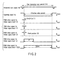
- the scanning signal Vy is a voltage Vyon supplied from a scanning voltage terminal and output within one horizontal scan period (1H) as shown in FIG. 2.
- Each electron-emitter 11 is driven or turned on to provide the electron beam that excites the corresponding phosphor 12 when the sum of the scanning signal Vy (the voltage on the scanning electrode) and the PWM drive signal Vx (the voltage on the signal electrode) exceeds the driving threshold.
- T is preset to a period equal to, for example, 1/1024 of the effective video period in one horizontal scan period (1H). This prevents the pulse width of the PWM drive signal from exceeding the effective video period even in the 1023rd gradation that is the maximum gradation level of the video signal.
- the Y driver 3 drives the scanning line Y1 with a scanning signal Vy
- the X driver 2 drives the signal lines X1, X2, X3, ... with PWM drive signals Vx having pulse widths corresponding to levels of the video signal for one horizontal line.
- the signal line X1 is driven with a PWM drive signal Vx having a pulse width corresponding to the jth gradation.
- the signal line X2 is driven with a PWM drive signal Vx having a pulse width corresponding to the 0th gradation.
- the signal line X3 is driven with a PWM drive signal Vx having a pulse width corresponding to the 0th gradation.
- the minimum value of the pulse widths of the PWM drive signals Vx for all the signal lines X1 - Xn is set to a value larger than zero. Since emitter discharge tends to occur upon remarkable signal transition, there is a very high probability that it will occur at the rise of the pulse. Therefore, in this driving method, when discharge is carried out in the electron-emitter 11 of a pixel PX which should emit light, a positive voltage (Vx')is temporarily applied to each of the signal lines X connected to the electron-emitters 11 of other pixels PX which are present on the same scanning line Y as that pixel but should not emit light.
- the pulse width corresponding to the 0th gradation is a.
- the pulse width a is set to a value which satisfies 0 ⁇ a ⁇ T, say, 10 ns. With such a pulse which is extremely short in width, the gradation visibility of each pixel PX will not be impaired.
- all the pixel voltages of the pixels PX on one horizontal line are increased to a value exceeding the driving threshold upon driving of each scanning line Y. That is, of pixels PX on one horizontal line, pixels PX which should not emit light have their electron-emitters supplied with a positive voltage from corresponding signal lines X. This suppresses the effective voltage applied to the electron-emitters 11 of pixels PX which should not emit light as the potential difference between the potential on the corresponding scanning line X which instantaneously transitions as the result of discharge of a pixel PX which should emit light and the potential on the corresponding signal lines X. Thus, the discharge damage can be relieved.
- the X driver 3 is configured to set the minimum value of the pulse widths of PWM drive signals corresponding to levels of a video signal for one horizontal line to a value larger than zero.
- the Y driver 2 may be configured to temporarily increase the voltage of the scanning signal Vy only upon driving of each scanning line Y as shown in FIG. 4. With that voltage of the scanning signal Vy, a pixel voltage exceeding the driving threshold Vth of the electron-emitters 11 is obtainable. Specifically, the voltage of the scanning signal Vy is increased for a period equal to the above-mentioned pulse width a. In this case, the minimum value of the pulse widths of the PWM drive signals Vx may be set to zero.
- the X driver 2 is configured to vary the luminance of each pixel PX with the pulse width of a corresponding PWM drive signal
- the luminance may be varied according to the pulse width and the voltage amplitude of the PWM drive signal.
- the scanning signal Vy is a negative voltage and the PWM drive signal Vx is a positive voltage
- their voltage polarity may be reversed. That is, the scanning signal Vy and the PWM drive signal Vx may be a positive voltage and a negative voltage, respectively.
- the present invention can be applied to a flat-panel display device, such as a field emission display (FED), in which a plurality of pixels are formed using surface-conduction electron-emitters by way of example.
- a field emission display FED
- a plurality of pixels are formed using surface-conduction electron-emitters by way of example.
Landscapes
- Engineering & Computer Science (AREA)
- Physics & Mathematics (AREA)
- Computer Hardware Design (AREA)
- General Physics & Mathematics (AREA)
- Theoretical Computer Science (AREA)
- Control Of Indicators Other Than Cathode Ray Tubes (AREA)
Abstract
A flat-panel display device includes a display panel 1 having scanning lines Y, signal lines X, and pixels PX which have electron-emitters 11 each of which is connected between a corresponding scanning line Y and a corresponding signal line X, and a drive circuit 2, 3, 4 which sequentially drives the scanning lines Y with a scanning signal and drives the signal lines X with drive signals while each of the scanning lines Y is being driven, the drive signals having pulse widths corresponding to levels of a video signal for one horizontal line and being of opposite voltage polarity to the scanning signal, to set, as the sum of the scanning signal and the drive signal, the pixel voltage applied to a pixel PX which should emit light to a value exceeding the driving threshold of the electron-emitters 11, and to set, as the sum of the scanning signal and the drive signal, the pixel voltage applied to a pixel PX which should emit light to a value less than the driving threshold of the electron-emitters 11. In particular, the drive circuit 2, 3, 4 is configured to temporarily increase the pixel voltage of the pixel PX which should not emit light, upon driving of each scanning line Y.
Description
- The present invention relates to a flat-panel display device, such as a field emission display (FED), in which a plurality of pixels are formed using surface-conduction electron-emitters by way of example and a display driving method.
- The FED generally includes a display panel and a drive circuit which drives that display panel. The display panel includes a plurality of scanning lines extending in the lateral (horizontal) direction, a plurality of signal lines extending in the longitudinal (vertical) direction to intersect the scanning lines, and a plurality of pixels located at the intersections between the scanning lines and the signal lines (see, for example,
JP-A No. 2002-221933 - The drive circuit includes a Y driver which is connected to one ends of the scanning lines and an X driver which is connected to one ends of the signal lines. The Y driver sequentially drives the scanning lines with a scanning signal. The X driver drives the signal lines with PWM drive signals having pulse widths corresponding to gradation levels of a video signal while each scanning line is being driven. Each pixel emits light in accordance with a pixel voltage between the corresponding signal and scanning lines, and the luminance thereof corresponds to an application period of the pixel voltage. Specifically, the scanning signal and the PWM drive signal set the potential Vy on the corresponding scanning line and the potential Vx on the corresponding signal line to Vy = -10.5V and Vx = +8V, thereby obtaining a pixel voltage of 18.5V between the scanning and signal lines to drive the electron-emitter. For pixels which should not emit light, the pulse widths of the PWM drive signals are set to zero to thereby keep the pixel voltage below the drive threshold of the electron-emitters.
- By the way, in the display operation of the conventional FED, there arises a problem that the in-plane luminance characteristic of the display panel degrades nonuniformly. A detailed analysis confirmed that the problem is caused by, when the electron-emitter of a certain pixel discharges, the electron-emitters arranged along the same scanning line suffering damage. The method of analysis was as follows: The entire display panel was displayed in one color with blue pixels (B). After the discharge, the entire display panel was displayed in white with red (R), green (G), and blue (B) pixels to confirm damage from luminance measurement. By making a comparison of the luminance after the discharge with that before the discharge, the degradation in luminance due to the discharge was analyzed.
- FIG. 5 shows a distribution of moving average values of the luminance ratio (luminance after discharge/luminance before discharge) obtained when the pixel in the plane coordinate position (315, 96) which is driven through the 315th signal line and the 96th scanning lines on the display panel is set as a point of discharge. Likewise, FIGS. 6, 7 and 8 show distributions of moving average values of the luminance ratio when the pixels in the plane coordinate positions (717, 182), (2997, 339) and (2787, 375) are each set as a point of discharge. Here, the points of discharge are all blue pixels. From FIGS. 5 through 8, it can be seen that the degree of spreading of damage differs according to the display color. The spreading of damage of the electron-emitter of the blue pixel which was driven at the time of discharge is small. The spreading of damage of the electron-emitters of the red and green pixels which were not driven at the time of discharge is large.
- The object of the present invention is to provide a flat-panel display device and a display driving method which allows discharge damage which spreads along scanning lines to be reduced.
- According to a first aspect of the present invention, there is provided a flat-panel display device which comprises a display panel having a plurality of scanning lines, a plurality of signal lines, and a plurality of pixels located near intersections between the scanning lines and the signal lines and having electron-emitters each of which is connected to a corresponding scanning line and a corresponding signal line; and a drive circuit which sequentially drives the scanning lines with a scanning signal and drives the signal lines by drive signals while each of the scanning lines is being driven, the drive signals having pulse widths corresponding to levels of a video signal for one horizontal line and being of opposite voltage polarity to the scanning signal, to set, as the sum of the scanning signal and the drive signal, the pixel voltage applied to a pixel which should emit light to a value exceeding the driving threshold of the electron-emitters, and to set, as the sum of the scanning signal and the drive signal, the pixel voltage applied to a pixel which should not emit light to a value less than the driving threshold of the electron-emitters; wherein the drive circuit is configured to temporarily increase the pixel voltage of at least the pixel which should not emit light, upon driving of each scanning line.
- According to a second aspect of the present invention, there is provided a display driving method for a display panel having a plurality of scanning lines, a plurality of signal lines, and a plurality of pixels located near intersections between the scanning lines and the signal lines and having electron-emitters each of which is connected to a corresponding scanning line and a corresponding signal line, which comprises sequentially driving the scanning lines with a scanning signal; driving the signal lines with drive signals while each of the scanning lines is being driven, the drive signals having pulse widths corresponding to levels of a video signal for one horizontal line and being of opposite voltage polarity to the scanning signal, to set, as the sum of the scanning signal and the drive signal, the pixel voltage applied to a pixel which should emit light to a value exceeding the driving threshold of the electron-emitters, and to set, as the sum of the scanning signal and the drive signal, the pixel voltage applied to a pixel which should not emit light to a value less than the driving threshold of the electron-emitters; and temporarily increasing the pixel voltage of at least the pixel which should not emit light, upon driving of each scanning line.
- With the flat-panel display device and the display driving method, the pixel voltage of the pixel which should not emit light is temporarily increased upon driving of each scanning line. This suppresses the effective voltage applied to each of the electron-emitters of pixels which should not emit light as the potential difference between the potential on the scanning line which makes an instant transition with discharge of a pixel which should emit light and the potential on the signal line, thus allowing discharge damage thereof to be relieved. Furthermore, when the pixel voltage is set to a value exceeding the driving threshold of the electron-emitters in its temporary increase, the effect of relieving the discharge damage will become more pronounced.
-
- FIG. 1 schematically shows the circuit configuration of a flat-panel display device according to an embodiment of the present invention.
- FIG. 2 is a timing diagram for use in explanation of the pulse width of a PWM drive signal produced in the flat-panel display device shown in FIG. 1.
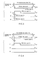
- FIG. 3 is a timing diagram for use in explanation of the PWM drive signal having a pulse width a shown in FIG. 2 and applied to a signal line for the 0th gradation of a video signal.
- FIG. 4 is a timing diagram for use in explanation of a modification that increases the voltage of a scanning signal shown in FIG. 2 in order to obtain a pixel voltage exceeding the driving threshold of the electron-emitters.
- FIG. 5 is a graph showing a distribution of moving average values of the luminance ratio when the pixel in the plane coordinate position (315, 96) is set as a point of discharge in a conventional display panel.
- FIG. 6 is a graph showing a distribution of moving average values of the luminance ratio when the pixel in the plane coordinate position (717, 182) is set as a point of discharge in the conventional display panel.
- FIG. 7 is a graph showing a distribution of moving average values of the luminance ratio when the pixel in the plane coordinate position (2997, 339) is set as a point of discharge in the conventional display panel.
- FIG. 8 is a graph showing a distribution of moving average values of the luminance ratio when the pixel in the plane coordinate position (2787, 375) is set as a point of discharge in the conventional display panel.
- A flat-panel display device according to an embodiment of the present invention will be described hereinafter with reference to the accompanying drawings. This flat-panel display device is a field emission display (FED) device having a resolution of n x m dots.
- FIG. 1 schematically shows the circuit configuration of the flat-panel display device. This flat-panel display panel has a
display panel 1, anX driver 2, aY driver 3, and avideo processing circuit 4. The display panel includes m number of scanning lines Y (Y1 - Ym) extending in the lateral (horizontal) direction, n number of signal lines X (X1 - Xn) extending in the longitudinal (vertical) direction to intersect the scanning lines Y1 - Ym, and m x n number of pixels PX located near intersections between the scanning lines Y1 - Ym and the signal lines X1 - Xn. Each color pixel unit includes three pixels PX which adjoin in the horizontal direction. In the color pixel unit, the three pixels PX are formed of surface-conduction electron-emitters 11 andphosphors 12 of red (R), green (G) and blue (B) which emit light by electron beams applied from the electron-emitters, respectively. Each of the scanning lines Y is used as a scanning electrode connected to the electron-emitters 11 of the pixels PX on a corresponding horizontal line. Each of the signal lines X is used as a signal electrode connected to the electron-emitters 11 of the pixels PX in a corresponding column. - The
X driver 2, theY driver 3 and thevideo processing circuit 4 are placed around thedisplay panel 1 as a display drive circuit. TheX driver 2 is a signal line driver which is connected one ends of the signal lines X1 - Xn. TheY driver 3 is a scanning line driver which is connected to one ends of the scanning lines Y1- Ym. Thevideo processing circuit 4 processes an RGB video signal supplied from an external signal source in digital form. The Y driver 3 sequentially drives the scanning lines Y1- Ym. TheX driver 2 drives the signal lines X1- Xn while each of the scanning lines Y1- Ym is being driven by theY driver 3. - The
video processing circuit 4 includes anAPL detection circuit 40 which totals levels of the RGB video signal for one frame or the like to detect the average level and anABL circuit 41 which corrects the RGB video signal on the basis of the average level detected by theAPL detection circuit 40 to uniformly lower the luminance for an image pattern which is large in the area of a high-luminance portion. TheAPL detection circuit 40 may be configured to detect the average gradation level of the RGB video signal for one or more frames or horizontal lines, from discharge current or emission currents actually flowing through the pixels PX. - The
X driver 2 includes aline memory 20 which samples and holds levels of the video signal for one horizontal line, which is supplied from thevideo processing circuit 4 in synchronism with a horizontal sync signal HD, and a drivesignal producing circuit 21 which produces n number of PWM drive signals Vx corresponding to levels of the video signal for one frame held in theline memory 20. The drivesignal producing circuit 21 includes n number of pulsewidth modulation circuits 22 each of which produces a pulse signal of a pulse width proportional to the gradation level of the video signal for the corresponding pixel PX, and n number ofoutput buffers 23 each of which outputs a reference voltage Vref from a driving reference voltage terminal as a PWM drive signal Vx to a corresponding one of the signal lines X1 - Xn during a period of time equal to the pulse width of the pulse signal from the corresponding pulsewidth modulation circuit 22. Each of the pulsewidth modulation circuits 22 is capable of setting pulse widths corresponding to, for example, 1024 gradations from the 0th gradation that is the minimum level of the video signal to the 1023rd gradation that is the maximum level of the input video signals. Here, the scanning signal Vy is set such that Vy = -10.5V and the PWM drive signal Vx is set such that Vx = +8V. - The
Y driver 3 includes ashift register 31 which shifts a vertical sync signal VD for each horizontal scan period to output it from one of its m output terminals, and m number ofoutput buffers 32 each of which responds to a pulse output from a corresponding one of the m outputs of the shift register to output a scanning signal Vy to a corresponding one of the scanning lines Y1 - Ym in one horizontal scan period (1H). The scanning signal Vy is a voltage Vyon supplied from a scanning voltage terminal and output within one horizontal scan period (1H) as shown in FIG. 2. Each electron-emitter 11 is driven or turned on to provide the electron beam that excites thecorresponding phosphor 12 when the sum of the scanning signal Vy (the voltage on the scanning electrode) and the PWM drive signal Vx (the voltage on the signal electrode) exceeds the driving threshold. - As shown in FIG. 2, the pulse width of the PWM drive signal is set to a (here a = 10 ns) for the 0th gradation, to T (here T > a) for the 1st gradation, and to j x T for the jth gradation. Here, T is preset to a period equal to, for example, 1/1024 of the effective video period in one horizontal scan period (1H). This prevents the pulse width of the PWM drive signal from exceeding the effective video period even in the 1023rd gradation that is the maximum gradation level of the video signal.
- While the
Y driver 3 drives the scanning line Y1 with a scanning signal Vy, theX driver 2 drives the signal lines X1, X2, X3, ... with PWM drive signals Vx having pulse widths corresponding to levels of the video signal for one horizontal line. In the example shown in FIG. 3, the signal line X1 is driven with a PWM drive signal Vx having a pulse width corresponding to the jth gradation. The signal line X2 is driven with a PWM drive signal Vx having a pulse width corresponding to the 0th gradation. The signal line X3 is driven with a PWM drive signal Vx having a pulse width corresponding to the 0th gradation. In this manner, the minimum value of the pulse widths of the PWM drive signals Vx for all the signal lines X1 - Xn is set to a value larger than zero. Since emitter discharge tends to occur upon remarkable signal transition, there is a very high probability that it will occur at the rise of the pulse. Therefore, in this driving method, when discharge is carried out in the electron-emitter 11 of a pixel PX which should emit light, a positive voltage (Vx')is temporarily applied to each of the signal lines X connected to the electron-emitters 11 of other pixels PX which are present on the same scanning line Y as that pixel but should not emit light. In the event that the electron-emitter 11 of a pixel PX which should emit light discharges actually, a transition instantaneously raised to the positive side (ΔVy: about 30V) occurs in the potential on the scanning line Y connected to that electron-emitter 11. Thus, the potential on the scanning line Y immediately after discharge can be expressed as ΔVy - |Vy| (here Vy is -10.5V mentioned above). If there is no positive voltage supplied to the signal lines X allocated for pixels PX which should not emit light, that transition voltage would be applied to their electron-emitters 11. However, in the case where a positive voltage of Vx' is supplied to these signal lines X, the effective voltage applied to the electron-emitters will become (ΔVy - | Vy | ) - Vx'. Thus, the load is relieved by Vx' and correspondingly the margin for emitter deterioration can be made large. Here, the pulse width corresponding to the 0th gradation is a. The pulse width a is set to a value which satisfies 0 < a < T, say, 10 ns. With such a pulse which is extremely short in width, the gradation visibility of each pixel PX will not be impaired. - With the flat-panel display device of this embodiment, all the pixel voltages of the pixels PX on one horizontal line are increased to a value exceeding the driving threshold upon driving of each scanning line Y. That is, of pixels PX on one horizontal line, pixels PX which should not emit light have their electron-emitters supplied with a positive voltage from corresponding signal lines X. This suppresses the effective voltage applied to the electron-
emitters 11 of pixels PX which should not emit light as the potential difference between the potential on the corresponding scanning line X which instantaneously transitions as the result of discharge of a pixel PX which should emit light and the potential on the corresponding signal lines X. Thus, the discharge damage can be relieved. - The present invention is not limited to the above embodiment and may be modified in various ways without departing from the scope thereof.
- In the above embodiment, the
X driver 3 is configured to set the minimum value of the pulse widths of PWM drive signals corresponding to levels of a video signal for one horizontal line to a value larger than zero. Instead, theY driver 2 may be configured to temporarily increase the voltage of the scanning signal Vy only upon driving of each scanning line Y as shown in FIG. 4. With that voltage of the scanning signal Vy, a pixel voltage exceeding the driving threshold Vth of the electron-emitters 11 is obtainable. Specifically, the voltage of the scanning signal Vy is increased for a period equal to the above-mentioned pulse width a. In this case, the minimum value of the pulse widths of the PWM drive signals Vx may be set to zero. - Although, in the above-stated embodiment, the
X driver 2 is configured to vary the luminance of each pixel PX with the pulse width of a corresponding PWM drive signal, the luminance may be varied according to the pulse width and the voltage amplitude of the PWM drive signal. - Although, in the above-stated embodiment, the scanning signal Vy is a negative voltage and the PWM drive signal Vx is a positive voltage, their voltage polarity may be reversed. That is, the scanning signal Vy and the PWM drive signal Vx may be a positive voltage and a negative voltage, respectively.
- The present invention can be applied to a flat-panel display device, such as a field emission display (FED), in which a plurality of pixels are formed using surface-conduction electron-emitters by way of example.
Claims (8)
- A flat-panel display device comprising:a display panel having a plurality of scanning lines, a plurality of signal lines, and a plurality of pixels located near intersections between said scanning lines and said signal lines and having electron-emitters each of which is connected to a corresponding scanning line and a corresponding signal line; anda drive circuit which sequentially drives said scanning lines with a scanning signal and drives said signal lines by drive signals while each of said scanning lines is being driven, said drive signals having pulse widths corresponding to levels of a video signal for one horizontal line and being of opposite voltage polarity to said scanning signal, to set, as the sum of said scanning signal and said drive signal, the pixel voltage applied to a pixel which should emit light to a value exceeding the driving threshold of said electron-emitters, and to set, as the sum of said scanning signal and said drive signal, the pixel voltage applied to a pixel which should not emit light to a value less than the driving threshold of said electron-emitters;characterized in that said drive circuit is configured to temporarily increase the pixel voltage of at least said pixel which should not emit light, upon driving of each scanning line.
- The flat-panel display device according to claim 1, characterized in that said drive circuit includes a signal line driver which sets the minimum value of the pulse widths of said drive signals corresponding to the levels of said video signal for one horizontal line to a value larger than zero to temporarily increase the pixel voltage applied to said pixel which should not emit light.
- The flat-panel display device according to claim 1, characterized in that said drive circuit includes a scanning line driver which increases the voltage of said scanning signal to temporarily increase the pixel voltage applied to said pixel which should not emit light.
- The flat-panel display device according to anyone of claims 1 to 3, characterized in that the pixel voltage of said pixel which should not emit light is set to a value exceeding the driving threshold of said electron-emitters in the temporary increase.
- A display driving method for a display panel having a plurality of scanning lines, a plurality of signal lines, and a plurality of pixels located near intersections between said scanning lines and said signal lines and having electron-emitters each of which is connected to a corresponding scanning line and a corresponding signal line, said method characterized by comprising:sequentially driving said scanning lines with a scanning signal;driving said signal lines with drive signals while each of said scanning lines is being driven, said drive signals having pulse widths corresponding to levels of a video signal for one horizontal line and being of opposite voltage polarity to said scanning signal, to set, as the sum of said scanning signal and said drive signal, the pixel voltage applied to a pixel which should emit light to a value exceeding the driving threshold of said electron-emitters, and to set, as the sum of said scanning signal and said drive signal, the pixel voltage applied to a pixel which should not emit light to a value less than the driving threshold of said electron-emitters; andtemporarily increasing the pixel voltage of at least said pixel which should not emit light, upon driving of each scanning line.
- The display driving method according to claim 5, characterized in that the method comprises setting the minimum value of the pulse widths of said drive signals corresponding to the levels of said video signal for one horizontal line to a value larger than zero to temporarily increase the pixel voltage applied to said pixel which should not emit light.
- The display driving method according to claim 5, characterized in that the method comprises increasing the voltage of said scanning signal to temporarily increase the pixel voltage applied to said pixel which should not emit light.
- The display driving method according to anyone of claims 5 to 7, characterized in that the method comprises setting the pixel voltage of said pixel which should not emit light to a value exceeding the driving threshold of said electron-emitters in the temporary increase.
Applications Claiming Priority (2)
| Application Number | Priority Date | Filing Date | Title |
|---|---|---|---|
| JP2004376765A JP2006184458A (en) | 2004-12-27 | 2004-12-27 | Flat display device and display driving method |
| PCT/JP2005/023349 WO2006070640A1 (en) | 2004-12-27 | 2005-12-20 | Flat display unit and displaying drive method |
Publications (2)
| Publication Number | Publication Date |
|---|---|
| EP1833039A1 true EP1833039A1 (en) | 2007-09-12 |
| EP1833039A4 EP1833039A4 (en) | 2008-01-23 |
Family
ID=36614759
Family Applications (1)
| Application Number | Title | Priority Date | Filing Date |
|---|---|---|---|
| EP05820223A Withdrawn EP1833039A4 (en) | 2004-12-27 | 2005-12-20 | Flat display unit and displaying drive method |
Country Status (5)
| Country | Link |
|---|---|
| US (1) | US20070247403A1 (en) |
| EP (1) | EP1833039A4 (en) |
| JP (1) | JP2006184458A (en) |
| TW (1) | TW200629203A (en) |
| WO (1) | WO2006070640A1 (en) |
Families Citing this family (1)
| Publication number | Priority date | Publication date | Assignee | Title |
|---|---|---|---|---|
| CN103680386B (en) * | 2013-12-18 | 2016-03-09 | 深圳市华星光电技术有限公司 | For GOA circuit and the display device of flat pannel display |
Family Cites Families (5)
| Publication number | Priority date | Publication date | Assignee | Title |
|---|---|---|---|---|
| US5578906A (en) * | 1995-04-03 | 1996-11-26 | Motorola | Field emission device with transient current source |
| JP3278375B2 (en) * | 1996-03-28 | 2002-04-30 | キヤノン株式会社 | Electron beam generator, image display device including the same, and method of driving them |
| JPH11231834A (en) * | 1998-02-13 | 1999-08-27 | Pioneer Electron Corp | Luminescent display device and its driving method |
| JPH11352923A (en) * | 1998-06-05 | 1999-12-24 | Canon Inc | Image display method and apparatus |
| JP2000250471A (en) * | 1999-02-25 | 2000-09-14 | Canon Inc | Driving apparatus and method for multi electron source and image forming apparatus |
-
2004
- 2004-12-27 JP JP2004376765A patent/JP2006184458A/en active Pending
-
2005
- 2005-12-20 EP EP05820223A patent/EP1833039A4/en not_active Withdrawn
- 2005-12-20 WO PCT/JP2005/023349 patent/WO2006070640A1/en not_active Ceased
- 2005-12-26 TW TW094146540A patent/TW200629203A/en unknown
-
2007
- 2007-06-27 US US11/768,945 patent/US20070247403A1/en not_active Abandoned
Non-Patent Citations (2)
| Title |
|---|
| No further relevant documents disclosed * |
| See also references of WO2006070640A1 * |
Also Published As
| Publication number | Publication date |
|---|---|
| WO2006070640A1 (en) | 2006-07-06 |
| TW200629203A (en) | 2006-08-16 |
| US20070247403A1 (en) | 2007-10-25 |
| EP1833039A4 (en) | 2008-01-23 |
| JP2006184458A (en) | 2006-07-13 |
Similar Documents
| Publication | Publication Date | Title |
|---|---|---|
| KR102322709B1 (en) | Image processing method, image processing circuit and display device using the same | |
| CN100401759C (en) | image display device | |
| US10546368B2 (en) | Method and device for compensating the perceptual bias of edge boost in a display panel | |
| KR20150102156A (en) | Display apparatus and method of driving the same | |
| US8508563B2 (en) | Image display apparatus and control method thereof | |
| JP4451057B2 (en) | Display device driving method, display device, and program thereof | |
| US20050134534A1 (en) | Flat-panel display device, display drive circuite and display drive method | |
| KR100552361B1 (en) | Display device | |
| WO2012132050A1 (en) | Display device, image processing device, image area detection method, and computer program | |
| JP4154422B2 (en) | Image display device | |
| US20070247403A1 (en) | Flat-panel display device and display driving method | |
| EP1983507A1 (en) | Image display device | |
| US12488725B2 (en) | Grayscale calibrating method for display panel and display device | |
| JP2012216184A (en) | Display device, image processing device, image area detecting method, and computer program | |
| KR100965577B1 (en) | LCD and its driving method | |
| JP4503669B2 (en) | Display device driving method, display device, and program thereof | |
| US20060066523A1 (en) | Display device and display method | |
| JP2005316108A (en) | Flat display device and display control circuit | |
| EP4485441A1 (en) | Brightness compensation for camera under display subpixels | |
| KR100536248B1 (en) | A plasma display panel, a luminance control device and method thereof | |
| KR101017186B1 (en) | LCD and its driving method | |
| KR100480167B1 (en) | Apparatus and method of driving plasma display panel | |
| JP2006106145A (en) | Display device | |
| JP2005107193A (en) | Flat display device, display control circuit, and display control method | |
| JP2006154665A (en) | Flat display device, display driving circuit, and display driving method |
Legal Events
| Date | Code | Title | Description |
|---|---|---|---|
| PUAI | Public reference made under article 153(3) epc to a published international application that has entered the european phase |
Free format text: ORIGINAL CODE: 0009012 |
|
| 17P | Request for examination filed |
Effective date: 20070626 |
|
| AK | Designated contracting states |
Kind code of ref document: A1 Designated state(s): DE FR GB IT NL |
|
| A4 | Supplementary search report drawn up and despatched |
Effective date: 20071221 |
|
| STAA | Information on the status of an ep patent application or granted ep patent |
Free format text: STATUS: THE APPLICATION HAS BEEN WITHDRAWN |
|
| DAX | Request for extension of the european patent (deleted) | ||
| RBV | Designated contracting states (corrected) |
Designated state(s): DE FR GB IT NL |
|
| 18W | Application withdrawn |
Effective date: 20080225 |