EP1830352A1 - Patterned medium and production method therefor - Google Patents
Patterned medium and production method therefor Download PDFInfo
- Publication number
- EP1830352A1 EP1830352A1 EP07000892A EP07000892A EP1830352A1 EP 1830352 A1 EP1830352 A1 EP 1830352A1 EP 07000892 A EP07000892 A EP 07000892A EP 07000892 A EP07000892 A EP 07000892A EP 1830352 A1 EP1830352 A1 EP 1830352A1
- Authority
- EP
- European Patent Office
- Prior art keywords
- magnetic material
- layer
- patterned medium
- magnetic
- medium according
- Prior art date
- Legal status (The legal status is an assumption and is not a legal conclusion. Google has not performed a legal analysis and makes no representation as to the accuracy of the status listed.)
- Granted
Links
- 238000004519 manufacturing process Methods 0.000 title claims description 17
- 239000000696 magnetic material Substances 0.000 claims abstract description 116
- 239000000758 substrate Substances 0.000 claims abstract description 26
- 238000000034 method Methods 0.000 claims description 38
- 239000000470 constituent Substances 0.000 claims description 13
- 239000000463 material Substances 0.000 claims description 13
- 238000001755 magnetron sputter deposition Methods 0.000 claims description 6
- 229910052804 chromium Inorganic materials 0.000 claims description 3
- 238000000059 patterning Methods 0.000 claims description 3
- 229910052697 platinum Inorganic materials 0.000 claims description 3
- 238000010586 diagram Methods 0.000 description 12
- 239000000314 lubricant Substances 0.000 description 5
- 238000004364 calculation method Methods 0.000 description 3
- 230000006835 compression Effects 0.000 description 3
- 238000007906 compression Methods 0.000 description 3
- VYPSYNLAJGMNEJ-UHFFFAOYSA-N Silicium dioxide Chemical compound O=[Si]=O VYPSYNLAJGMNEJ-UHFFFAOYSA-N 0.000 description 2
- 239000013590 bulk material Substances 0.000 description 2
- TWNQGVIAIRXVLR-UHFFFAOYSA-N oxo(oxoalumanyloxy)alumane Chemical compound O=[Al]O[Al]=O TWNQGVIAIRXVLR-UHFFFAOYSA-N 0.000 description 2
- 238000005498 polishing Methods 0.000 description 2
- 229910052814 silicon oxide Inorganic materials 0.000 description 2
- 238000004088 simulation Methods 0.000 description 2
- 239000000126 substance Substances 0.000 description 2
- 229910001069 Ti alloy Inorganic materials 0.000 description 1
- 238000001816 cooling Methods 0.000 description 1
- 238000001312 dry etching Methods 0.000 description 1
- 229910052751 metal Inorganic materials 0.000 description 1
- 239000002184 metal Substances 0.000 description 1
- 230000004048 modification Effects 0.000 description 1
- 238000012986 modification Methods 0.000 description 1
- 230000008520 organization Effects 0.000 description 1
- 238000003825 pressing Methods 0.000 description 1
- 229910052715 tantalum Inorganic materials 0.000 description 1
- 229910052721 tungsten Inorganic materials 0.000 description 1
- 238000001039 wet etching Methods 0.000 description 1
Images



Classifications
-
- G—PHYSICS
- G11—INFORMATION STORAGE
- G11B—INFORMATION STORAGE BASED ON RELATIVE MOVEMENT BETWEEN RECORD CARRIER AND TRANSDUCER
- G11B5/00—Recording by magnetisation or demagnetisation of a record carrier; Reproducing by magnetic means; Record carriers therefor
- G11B5/62—Record carriers characterised by the selection of the material
- G11B5/64—Record carriers characterised by the selection of the material comprising only the magnetic material without bonding agent
- G11B5/66—Record carriers characterised by the selection of the material comprising only the magnetic material without bonding agent the record carriers consisting of several layers
- G11B5/667—Record carriers characterised by the selection of the material comprising only the magnetic material without bonding agent the record carriers consisting of several layers including a soft magnetic layer
-
- G—PHYSICS
- G11—INFORMATION STORAGE
- G11B—INFORMATION STORAGE BASED ON RELATIVE MOVEMENT BETWEEN RECORD CARRIER AND TRANSDUCER
- G11B5/00—Recording by magnetisation or demagnetisation of a record carrier; Reproducing by magnetic means; Record carriers therefor
- G11B5/84—Processes or apparatus specially adapted for manufacturing record carriers
- G11B5/855—Coating only part of a support with a magnetic layer
-
- G—PHYSICS
- G11—INFORMATION STORAGE
- G11B—INFORMATION STORAGE BASED ON RELATIVE MOVEMENT BETWEEN RECORD CARRIER AND TRANSDUCER
- G11B5/00—Recording by magnetisation or demagnetisation of a record carrier; Reproducing by magnetic means; Record carriers therefor
- G11B5/62—Record carriers characterised by the selection of the material
- G11B5/64—Record carriers characterised by the selection of the material comprising only the magnetic material without bonding agent
- G11B5/65—Record carriers characterised by the selection of the material comprising only the magnetic material without bonding agent characterised by its composition
-
- G—PHYSICS
- G11—INFORMATION STORAGE
- G11B—INFORMATION STORAGE BASED ON RELATIVE MOVEMENT BETWEEN RECORD CARRIER AND TRANSDUCER
- G11B5/00—Recording by magnetisation or demagnetisation of a record carrier; Reproducing by magnetic means; Record carriers therefor
- G11B5/62—Record carriers characterised by the selection of the material
- G11B5/64—Record carriers characterised by the selection of the material comprising only the magnetic material without bonding agent
- G11B5/66—Record carriers characterised by the selection of the material comprising only the magnetic material without bonding agent the record carriers consisting of several layers
-
- Y—GENERAL TAGGING OF NEW TECHNOLOGICAL DEVELOPMENTS; GENERAL TAGGING OF CROSS-SECTIONAL TECHNOLOGIES SPANNING OVER SEVERAL SECTIONS OF THE IPC; TECHNICAL SUBJECTS COVERED BY FORMER USPC CROSS-REFERENCE ART COLLECTIONS [XRACs] AND DIGESTS
- Y10—TECHNICAL SUBJECTS COVERED BY FORMER USPC
- Y10S—TECHNICAL SUBJECTS COVERED BY FORMER USPC CROSS-REFERENCE ART COLLECTIONS [XRACs] AND DIGESTS
- Y10S428/00—Stock material or miscellaneous articles
- Y10S428/90—Magnetic feature
Definitions
- the present invention relates to a patterned medium preferable for a magnetic disc memory device such as a hard disc device.
- the patterned medium has an advantage of obtaining a high areal density, it is disadvantageous in that an error may be generated in recording and reproduction due to deformation of the projecting portion caused by collision of the lower end of the magnetic head with a projecting portion of the recording layer.
- An object of the present invention is to provide a highly reliable patterned medium without generating an error in recording and reproduction, and a magnetic disc memory device using the same.
- a patterned medium has a substrate, a soft magnetic layer, a non-magnetic layer, an intermediate layer and a recording layer.
- the recording layer has a pattern structure of a non-magnetic material and a magnetic material, and the Young's modulus of the non-magnetic material is larger than the Young's modulus of the magnetic material.
- a highly reliable patterned medium without generating an error in recording and reproduction can be provided.
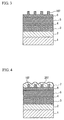
- FIG. 1 shows a first embodiment of a patterned medium of the present invention.
- the patterned medium of this embodiment has a substrate 1, a pre-coat layer 2 thereon, a soft magnetic layer 3, a non magnetic layer 4, a soft magnetic layer 5, an intermediate layer 6, a recording layer 7, a protection layer 8 and a lubricant layer 9.
- the recording layer 7 has a pattern structure of a non-magnetic member 107 and a magnetic member 207.
- the pre-coat layer 2, the soft magnetic layer 3, the non magnetic layer 4, the soft magnetic layer 5, the intermediate layer 6, and the recording layer 7 are made of a metal, and they are formed by for example a DC magnetron sputtering method. It is preferable that the soft magnetic layers 3, 5 are made of an amorphous material.
- the intermediate layer 6 includes Ru as the principal constituent element, and it also contains as the additional elements, Ti by a concentration of 0.14 at% or more and 25 at% or less.
- the principal constituent element denotes the element included by the largest atomic percent
- the production method for a patterned medium of the present invention in particular, the method for forming the pattern structure of the recording layer 7 will be explained.
- the pre-coat layer 2, the soft magnetic layer 3, the non-magnetic layer 4, the soft magnetic layer 5, and the intermediate layer 6 are formed on the substrate 1, and furthermore, the non magnetic material layer 107 is formed thereon.
- the non-magnetic material layer 107 may be formed by for example a DC magnetron sputtering method. Since the method for forming the pre-coat layer 2, the soft magnetic layer 3, the non magnetic layer 4, the soft magnetic layer 5, and the intermediate layer 6 on the substrate 1 is already known, explanation thereof will not be described here.
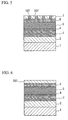
- the non-magnetic material layer 107 is patterned. That is, a projecting and recessed pattern of the non-magnetic material layer 107 is formed. Since the thickness of the recessed portion of the non-magnetic material layer 107 is minute, in FIG 3, only the projecting portion is drawn without showing the recessed portion.
- the pattern may be formed by for example a nano imprint method.
- the nano imprint method is a method of patterning the non magnetic material layer 107 by pressing a high temperature mold having a projecting and recessed pattern against the non magnetic material layer 107 and cooling down. Instead of using the nano imprint method, dry etching or wet etching with a mask having a pattern may be utilized as well.
- the pattern may be formed by self organization.
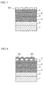
- the magnetic material layer 207 is formed so as to fill up the recessed portion of the projecting and recessed pattern of the non-magnetic material layer 107.
- the magnetic material layer 207 may be formed so as to completely fill up the recessed portion of the non-magnetic material layer 107 and furthermore overflow the recessed portion.
- the magnetic material layer 207 is formed by for example a DC magnetron sputtering method.
- the outer surface of the magnetic material layer 207 is flattened. The flattening operation is carried out by for example a chemical mechanical polishing (CMP). The flattening process may be eliminated.
- CMP chemical mechanical polishing
- the protection layer 8 and the lubricant layer 9 are formed. Since the method for forming the protection layer 8 and the lubricant layer 9 is already known, explanation thereof will not be described here.
- the pre-coat layer 2, the soft magnetic layer 3, the non-magnetic layer 4, the soft magnetic layer 5, and the intermediate layer 6 are formed on the substrate 1, and furthermore, the magnetic material layer 207 is formed thereon.
- the magnetic material layer 207 may be formed by for example a DC magnetron sputtering method.
- the magnetic material layer 207 is patterned. That is, a projecting and recessed pattern of the magnetic material layer 207 is formed. Since the thickness of the recessed portion of the magnetic material layer 207 is minute, in FIG. 7, only the projecting portion is drawn without showing the recessed portion.
- the pattern may be formed by for example a nano imprint method.
- the non-magnetic material layer 107 is formed so as to fill up the recessed portion of the projecting and recessed pattern of the magnetic material layer 207.
- the non-magnetic material layer 107 may be formed so as to completely fill up the recessed portion of the magnetic material layer 207 and furthermore overflow the recessed portion.
- the non-magnetic material layer 107 is formed by for example a DC magnetron sputtering method.
- the outer surface of the non-magnetic material layer 107 is flattened. The flattening operation is carried out by for example a chemical mechanical polishing (CMP). The flattening process may be eliminated.
- CMP chemical mechanical polishing
- the protection layer 8 and the lubricant layer 9 are formed. Since the method for forming the protection layer 8 and the lubricant layer 9 is already known, explanation thereof will not be described here.
- the magnetic material layer 207 is formed so as to fill up the recessed portion of the projecting and recessed pattern of the non magnetic layer 107 in the first method, whereas the non magnetic material layer 107 is formed so as to fill up the recessed portion of the projecting and recessed pattern of the magnetic material layer 207 in the second method.
- the volume ratio of the non magnetic material layer 107 to the magnetic material layer 207 in the recording layer formed by the second method is equal to the volume ratio of the non magnetic material layer 107 to the magnetic material layer 207 in the recording layer formed by the first method. Therefore, the projecting and recessed pattern of the magnetic material layer 207 used in the second method is in the inverse relationship with the projecting and recessed pattern of the non-magnetic material layer 107 used in the first method.
- FIG. 10 shows a second embodiment of a patterned medium of the present invention.
- the base layer 106 is provided between the soft magnetic layer 5 and the intermediate layer 6.
- the base layer 106 is made of for example a Ti alloy.
- FIG. 11 shows a third embodiment of a patterned medium of the present invention.
- the soft magnetic layer 103 is provided instead of the soft magnetic layer 3, the non-magnetic layer 4 and the soft magnetic layer 5 in the first and second embodiments.
- the pattern structure of the recording layer 7 is formed by the method mentioned above.
- the present inventors have found out that deformation of the patterned medium in the surface direction can be restrained when the magnetic head contacts with the patterned medium in the case the Young's modulus of the non magnetic material layer 107 is larger than the Young's modulus of the magnetic material layer 207 in the recording layer 7 of a patterned medium according to the present invention.
- FIG. 12 shows the result of calculation of the molecular kinetic simulation carried out by the present inventors.
- the magnetic material layer 207 a material containing Co, Cr, and Pt with a 284 GPa Young's modulus was used.
- the surface distortion of the recording layer was calculated with the Young's modulus of the non-magnetic material layer 107 changed.
- the distortion in the direction parallel to the substrate surface in the case the magnetic material layer 207 is pressed in the direction perpendicular to the substrate surface and the distortion in the direction perpendicular to the substrate surface was 0.003 was calculated.
- the vertical axis denotes the distortion in the direction parallel to the substrate surface, and a positive value is pulling and a negative value is compression.
- the lateral axis denotes the ratio En/Em of the Young's modulus En of the non-magnetic material layer 107 to the Young's modulus Em of the magnetic material layer 207.
- the solid line curve shows the calculation result in the case the volume ratio of the non magnetic material layer 107 to the magnetic material layer 207 in the recording layer 7 is 1, and the broken line curve shows the result in the case the volume ratio of the non magnetic material layer 107 to the magnetic material layer 207 in the recording layer 7 is 0.7.
- the distortion amount is smaller in the case of the 0.7 volume ratio of the non-magnetic material layer 107 to the magnetic material layer 207 than the case of the 1 volume ratio.
- the thickness of the magnetic material layer 207 and that of the non-magnetic material layer 107 are substantially same. Therefore, the volume ratio of the non-magnetic material layer 107 to the magnetic material layer 207 is substantially equal to the area ratio of the non-magnetic material layer 107 to the magnetic material layer 207 in the pattern. Therefore, the shape or the design of the pattern may be produced so as to have a 0.7 area ratio of the non-magnetic material layer 107 to the magnetic material layer 207.
- the non-magnetic material layer 107 a silicon oxide layer or an aluminum oxide layer is used as the non-magnetic material layer 107.
- the Young's modulus of the silicon oxide layer is about 70 GPa.
- the Young's modulus of the aluminum oxide differs between the case of a bulk material and the case of a layer. In the case of a bulk material, it is 200 GPa or more, and in the case of a layer, due to the low atomic number density, it is about 30 GPa to 150 GPa.
- the Young's modulus of the magnetic material 207 is about 200 GPa or more. Therefore, since En/EM ⁇ 1, as shown in FICx 12, tensile distortion is generated in the direction parallel to the substrate surface. This causes an error at the time of reading and writing information.
- the present inventors have selected the magnetic material layer 207 and the non-magnetic material layer 107 so as to have En/Em > 1.
- the magnetic material layer 207 a material having Co, Cr and Pt as the constituent elements is selected.
- the Cr concentration of the magnetic material layer 207 is 15 at% or more and 25 at% or less, and the Pt concentration is 10 at% or more and 20 at% or less.
- the Young's modulus of the magnetic material layer 207 is about 284 GPa.
- a material having W or Ta as the main constituent material is preferable as the non-magnetic material layer 107 for such a magnetic material layer 207.
- a constituent material W, WN, WC, WB, WO, or TaN, TaC, TaB can be presented.
- the Young's modulus of such a non-magnetic material layer 107 is sufficiently larger than 284 GPa, the Young's modulus of the magnetic material layer 207. Therefore, since En/Em > 1, generation of the tensile distortion can be restrained in the direction parallel to the substrate surface.
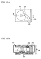
- FIG. 13 shows a hard disc device using a patterned medium of the present invention as the recording medium.
- FIG. 13A shows the planer configuration of the hard disc device
- FIG. 13B shows the cross-sectional configuration along the line A - A of the hard disc device of FIG. 13A.
- the top surface is eliminated.
- the hard disc device of this embodiment has a plurality of patterned media 201, a driving part 202 for rotating the patterned media, a magnetic head 203, a driving means for the magnetic head 204, and a recording and reproduction signal processing means for the magnetic head 205.
- the patterned media 201 are the patterned media according to the present invention shown in FIGS. 1, 10 and 11. Even in the case the magnetic head 203 is contacted with the patterned media 201, tensile distortion is restrained in the direction parallel to the substrate surface in the recording layer. Therefore, even in the case the head lift amount (distance between the head and the protection layer) becomes 10 nm or less, reliability of recording and reproduction is high.
Landscapes
- Magnetic Record Carriers (AREA)
- Manufacturing Of Magnetic Record Carriers (AREA)
- Thin Magnetic Films (AREA)
Abstract
Description
- The present invention relates to a patterned medium preferable for a magnetic disc memory device such as a hard disc device.
- Recently, the recording capacity of the magnetic discs such as a hard disc device has been dramatically increased. This is owing to the dramatic increase of the areal density of the magnetic disc. As a technique for increasing the areal density of the magnetic disc, a patterned medium with a recording layer formed by a projecting and recessed pattern can be presented.
[Patent Document 1]Japanese Patent Application Laid-Open No. 2005-122876 - Although the patterned medium has an advantage of obtaining a high areal density, it is disadvantageous in that an error may be generated in recording and reproduction due to deformation of the projecting portion caused by collision of the lower end of the magnetic head with a projecting portion of the recording layer.
- An object of the present invention is to provide a highly reliable patterned medium without generating an error in recording and reproduction, and a magnetic disc memory device using the same.
- According to the present invention, a patterned medium has a substrate, a soft magnetic layer, a non-magnetic layer, an intermediate layer and a recording layer. The recording layer has a pattern structure of a non-magnetic material and a magnetic material, and the Young's modulus of the non-magnetic material is larger than the Young's modulus of the magnetic material.
- According to the present invention, a highly reliable patterned medium without generating an error in recording and reproduction can be provided.
-
- FIG. 1 is a diagram showing the structure of a first embodiment of a patterned medium of the present invention.
- FIG 2 is a diagram for explaining a process of a first embodiment of a production method for a recording layer of a patterned medium of the present invention.
- FIG 3 is a diagram for explaining a process of the first embodiment of a production method for a recording layer of a patterned medium of the present invention.
- FIG. 4 is a diagram for explaining a process of the first embodiment of a production method for a recording layer of a patterned medium of the present invention.
- FIG 5 is a diagram for explaining a process of the first embodiment of a production method for a recording layer of a patterned medium of the present invention.
- FIG. 6 is a diagram for explaining a process of a second embodiment of a production method for a recording layer of a patterned medium of the present invention.
- FIG 7 is a diagram for explaining a process of the second embodiment of a production method for a recording layer of a patterned medium of the present invention.
- FIG. 8 is a diagram for explaining a process of the second embodiment of a production method for a recording layer of a patterned medium of the present invention.
- FIG. 9 is a diagram for explaining a process of the second embodiment of a production method for a recording layer of a patterned medium of the present invention.
- FIG 10 is a diagram showing the structure of the second embodiment of a patterned medium of the present invention.
- FIG 11 is a diagram showing the structure of the third embodiment of a patterned medium of the present invention.
- FIG. 12 is a graph showing the result of calculation of the distortion of a patterned medium in the direction parallel to the substrate surface of a recording layer by the molecular kinetic simulation.
- FIG. 13 is a diagram showing the configuration of a hard disc device using a patterned medium of the present invention.
- FIG. 1 shows a first embodiment of a patterned medium of the present invention. The patterned medium of this embodiment has a
substrate 1, apre-coat layer 2 thereon, a softmagnetic layer 3, a nonmagnetic layer 4, a softmagnetic layer 5, anintermediate layer 6, arecording layer 7, a protection layer 8 and alubricant layer 9. Therecording layer 7 has a pattern structure of anon-magnetic member 107 and amagnetic member 207. Thepre-coat layer 2, the softmagnetic layer 3, the nonmagnetic layer 4, the softmagnetic layer 5, theintermediate layer 6, and therecording layer 7 are made of a metal, and they are formed by for example a DC magnetron sputtering method. It is preferable that the softmagnetic layers intermediate layer 6 includes Ru as the principal constituent element, and it also contains as the additional elements, Ti by a concentration of 0.14 at% or more and 25 at% or less. The principal constituent element denotes the element included by the largest atomic percent concentration. - With reference to FIGS. 2 to 5, the production method for a patterned medium of the present invention, in particular, the method for forming the pattern structure of the
recording layer 7 will be explained. First, as shown in FIG 2, thepre-coat layer 2, the softmagnetic layer 3, thenon-magnetic layer 4, the softmagnetic layer 5, and theintermediate layer 6 are formed on thesubstrate 1, and furthermore, the nonmagnetic material layer 107 is formed thereon. Thenon-magnetic material layer 107 may be formed by for example a DC magnetron sputtering method. Since the method for forming thepre-coat layer 2, the softmagnetic layer 3, the nonmagnetic layer 4, the softmagnetic layer 5, and theintermediate layer 6 on thesubstrate 1 is already known, explanation thereof will not be described here. - Next, as shown in FIG. 3, the
non-magnetic material layer 107 is patterned. That is, a projecting and recessed pattern of thenon-magnetic material layer 107 is formed. Since the thickness of the recessed portion of thenon-magnetic material layer 107 is minute, in FIG 3, only the projecting portion is drawn without showing the recessed portion. The pattern may be formed by for example a nano imprint method. The nano imprint method is a method of patterning the nonmagnetic material layer 107 by pressing a high temperature mold having a projecting and recessed pattern against the nonmagnetic material layer 107 and cooling down. Instead of using the nano imprint method, dry etching or wet etching with a mask having a pattern may be utilized as well. Moreover, the pattern may be formed by self organization. - Next, as shown in FIG 4, the
magnetic material layer 207 is formed so as to fill up the recessed portion of the projecting and recessed pattern of thenon-magnetic material layer 107. As shown in the figure, themagnetic material layer 207 may be formed so as to completely fill up the recessed portion of thenon-magnetic material layer 107 and furthermore overflow the recessed portion. Themagnetic material layer 207 is formed by for example a DC magnetron sputtering method. Next, as shown in FIG 5, the outer surface of themagnetic material layer 207 is flattened. The flattening operation is carried out by for example a chemical mechanical polishing (CMP). The flattening process may be eliminated. Finally, as shown in FIG. 1, the protection layer 8 and thelubricant layer 9 are formed. Since the method for forming the protection layer 8 and thelubricant layer 9 is already known, explanation thereof will not be described here. - With reference to FIGS. 6 to 9, another embodiment of the method for forming the pattern structure of the
recording layer 7 of a patterned medium of the present invention will be explained. First, as shown in FIG 6, thepre-coat layer 2, the softmagnetic layer 3, thenon-magnetic layer 4, the softmagnetic layer 5, and theintermediate layer 6 are formed on thesubstrate 1, and furthermore, themagnetic material layer 207 is formed thereon. Themagnetic material layer 207 may be formed by for example a DC magnetron sputtering method. - Next, as shown in FIG 7, the
magnetic material layer 207 is patterned. That is, a projecting and recessed pattern of themagnetic material layer 207 is formed. Since the thickness of the recessed portion of themagnetic material layer 207 is minute, in FIG. 7, only the projecting portion is drawn without showing the recessed portion. The pattern may be formed by for example a nano imprint method. - Next, as shown in FIG 8, the
non-magnetic material layer 107 is formed so as to fill up the recessed portion of the projecting and recessed pattern of themagnetic material layer 207. As shown in the figure, thenon-magnetic material layer 107 may be formed so as to completely fill up the recessed portion of themagnetic material layer 207 and furthermore overflow the recessed portion. Thenon-magnetic material layer 107 is formed by for example a DC magnetron sputtering method. Next, as shown in FIG 9, the outer surface of thenon-magnetic material layer 107 is flattened. The flattening operation is carried out by for example a chemical mechanical polishing (CMP). The flattening process may be eliminated. Finally, as shown in FIG. 1, the protection layer 8 and thelubricant layer 9 are formed. Since the method for forming the protection layer 8 and thelubricant layer 9 is already known, explanation thereof will not be described here. - In making a comparison between the first method for forming a recording layer according to the present invention as explained with reference to FIGS. 2 to 5 and the second method for forming recording layer according to the present invention explained with reference to FIGS. 6 to 9, the
magnetic material layer 207 is formed so as to fill up the recessed portion of the projecting and recessed pattern of the nonmagnetic layer 107 in the first method, whereas the nonmagnetic material layer 107 is formed so as to fill up the recessed portion of the projecting and recessed pattern of themagnetic material layer 207 in the second method. However, the volume ratio of the nonmagnetic material layer 107 to themagnetic material layer 207 in the recording layer formed by the second method is equal to the volume ratio of the nonmagnetic material layer 107 to themagnetic material layer 207 in the recording layer formed by the first method. Therefore, the projecting and recessed pattern of themagnetic material layer 207 used in the second method is in the inverse relationship with the projecting and recessed pattern of thenon-magnetic material layer 107 used in the first method. - FIG. 10 shows a second embodiment of a patterned medium of the present invention. In this embodiment, the
base layer 106 is provided between the softmagnetic layer 5 and theintermediate layer 6. Thebase layer 106 is made of for example a Ti alloy. - FIG. 11 shows a third embodiment of a patterned medium of the present invention. In this embodiment, the soft
magnetic layer 103 is provided instead of the softmagnetic layer 3, thenon-magnetic layer 4 and the softmagnetic layer 5 in the first and second embodiments. In the patterned media of FIGS. 10 and 11, the pattern structure of therecording layer 7 is formed by the method mentioned above. - The present inventors have found out that deformation of the patterned medium in the surface direction can be restrained when the magnetic head contacts with the patterned medium in the case the Young's modulus of the non
magnetic material layer 107 is larger than the Young's modulus of themagnetic material layer 207 in therecording layer 7 of a patterned medium according to the present invention. - FIG. 12 shows the result of calculation of the molecular kinetic simulation carried out by the present inventors. As the
magnetic material layer 207, a material containing Co, Cr, and Pt with a 284 GPa Young's modulus was used. The surface distortion of the recording layer was calculated with the Young's modulus of thenon-magnetic material layer 107 changed. The distortion in the direction parallel to the substrate surface in the case themagnetic material layer 207 is pressed in the direction perpendicular to the substrate surface and the distortion in the direction perpendicular to the substrate surface was 0.003 was calculated. - The vertical axis denotes the distortion in the direction parallel to the substrate surface, and a positive value is pulling and a negative value is compression. The lateral axis denotes the ratio En/Em of the Young's modulus En of the
non-magnetic material layer 107 to the Young's modulus Em of themagnetic material layer 207. - The solid line curve shows the calculation result in the case the volume ratio of the non
magnetic material layer 107 to themagnetic material layer 207 in therecording layer 7 is 1, and the broken line curve shows the result in the case the volume ratio of the nonmagnetic material layer 107 to themagnetic material layer 207 in therecording layer 7 is 0.7. As it is apparent form the comparison between the broken line curve and the solid line curve, the distortion amount is smaller in the case of the 0.7 volume ratio of thenon-magnetic material layer 107 to themagnetic material layer 207 than the case of the 1 volume ratio. - The thickness of the
magnetic material layer 207 and that of thenon-magnetic material layer 107 are substantially same. Therefore, the volume ratio of thenon-magnetic material layer 107 to themagnetic material layer 207 is substantially equal to the area ratio of thenon-magnetic material layer 107 to themagnetic material layer 207 in the pattern. Therefore, the shape or the design of the pattern may be produced so as to have a 0.7 area ratio of thenon-magnetic material layer 107 to themagnetic material layer 207. - It is the tensile distortion in the direction parallel to the substrate surface in the
recording layer 7 that influences recording and reproduction of the patterned medium, and the compression distortion in the direction parallel to the substrate surface barely influences recording and reproduction. Therefore, only the tensile distortion in the direction parallel to the substrate surface in therecording layer 7 is discussed here. From FIG. 12, it is learned that tensile distortion is generated in the direction parallel to the substrate surface in the case En/Em < 1, with the value increased as the ratio En/Em becomes smaller. In the case En/Em > 1, the tensile distortion is not generated in the direction parallel to the substrate surface. That is, the compression distortion in the direction parallel to the substrate surface is generated, and the value is relatively small. Therefore, the Young's modulus En of thenon-magnetic material layer 107 needs to be larger than the Young's modulus Em of themagnetic material layer 207. - In the conventional patterned media, as the
non-magnetic material layer 107, a silicon oxide layer or an aluminum oxide layer is used. The Young's modulus of the silicon oxide layer is about 70 GPa. The Young's modulus of the aluminum oxide differs between the case of a bulk material and the case of a layer. In the case of a bulk material, it is 200 GPa or more, and in the case of a layer, due to the low atomic number density, it is about 30 GPa to 150 GPa. On the other hand, the Young's modulus of themagnetic material 207 is about 200 GPa or more. Therefore, since En/EM < 1, as shown in FICx 12, tensile distortion is generated in the direction parallel to the substrate surface. This causes an error at the time of reading and writing information. - Therefore, the present inventors have selected the
magnetic material layer 207 and thenon-magnetic material layer 107 so as to have En/Em > 1. As themagnetic material layer 207, a material having Co, Cr and Pt as the constituent elements is selected. The Cr concentration of themagnetic material layer 207 is 15 at% or more and 25 at% or less, and the Pt concentration is 10 at% or more and 20 at% or less. The Young's modulus of themagnetic material layer 207 is about 284 GPa. - It was found out that a material having W or Ta as the main constituent material is preferable as the
non-magnetic material layer 107 for such amagnetic material layer 207. As such a constituent material, W, WN, WC, WB, WO, or TaN, TaC, TaB can be presented. The Young's modulus of such anon-magnetic material layer 107 is sufficiently larger than 284 GPa, the Young's modulus of themagnetic material layer 207. Therefore, since En/Em > 1, generation of the tensile distortion can be restrained in the direction parallel to the substrate surface. - FIG. 13 shows a hard disc device using a patterned medium of the present invention as the recording medium. FIG. 13A shows the planer configuration of the hard disc device, and FIG. 13B shows the cross-sectional configuration along the line A - A of the hard disc device of FIG. 13A. In FIG. 13A, the top surface is eliminated.
- The hard disc device of this embodiment has a plurality of patterned
media 201, a drivingpart 202 for rotating the patterned media, amagnetic head 203, a driving means for themagnetic head 204, and a recording and reproduction signal processing means for themagnetic head 205. - The patterned
media 201 are the patterned media according to the present invention shown in FIGS. 1, 10 and 11. Even in the case themagnetic head 203 is contacted with the patternedmedia 201, tensile distortion is restrained in the direction parallel to the substrate surface in the recording layer. Therefore, even in the case the head lift amount (distance between the head and the protection layer) becomes 10 nm or less, reliability of recording and reproduction is high. - Although the embodiments of the present invention have been explained so far, the present invention is not limited to the above-mentioned embodiments, and it is easily understood by those in the art that various modification can be executed within the scope disclosed in the claims.
Claims (20)
- A patterned medium comprising a substrate (1), and a soft magnetic layer (3), a non magnetic layer (4), an intermediate layer (6) and a recording layer (7) formed successively on one principal plane side of the substrate (1), wherein the recording layer (7) has a pattern structure of a non magnetic material (107) and a magnetic material (207) such that the Young's modulus of the non magnetic material is larger than the Young's modulus of the magnetic material.
- The patterned medium according to claim 1, wherein the pattern structure of the recording layer (7) has a structure that the recessed portion of a projecting and recessed pattern of the non magnetic material (107) is filled up with the magnetic material (207).
- The patterned medium according to claim 1, wherein the pattern structure of the recording layer (7) has a structure that the recessed portion of a projecting and recessed pattern of the magnetic material (207) is filled up with the non magnetic material (107).
- The patterned medium according to claim 1, wherein the non-magnetic material (107) contains W as the main constituent material.
- The patterned medium according to claim 4, wherein the non-magnetic material (107) contains one selected from the group consisting of WN, WC, WB, and WO as the main constituent material.
- The patterned medium according to claim 1, wherein the non-magnetic material (107) contains Ta as the main constituent material.
- The patterned medium according to claim 6, wherein the non-magnetic material (107) contains one selected from the group consisting of TaN, TaC, and TaB as the main constituent material.
- The patterned medium according to claim 1, wherein the magnetic material (207) contains Co, Cr and Pt as the constituent element with the Cr concentration of 15 at% or more and 25 at% or less, and the Pt concentration is 10 at% or more and 20 at% or less.
- The patterned medium according to claim 1, wherein the soft magnetic layer (3) is made of an amorphous material, and the intermediate layer (6) contains Ru as the main constituent element.
- The patterned medium according to claim 9, wherein the intermediate layer (6) contains Ti as an additional element.
- A production method for a patterned medium comprising the steps of forming a soft magnetic layer (3), a non magnetic layer (4) and an intermediate layer (6) successively on one principal plane side of a substrate (1), forming a non magnetic material layer on the intermediate layer (6), forming a projecting and recessed pattern of the non magnetic material (107) by patterning the non magnetic material layer, and forming a magnetic material layer (207) so as to fill up the recessed portion of the projecting and recessed pattern of the non magnetic material (107), wherein the Young's modulus of the non magnetic material is larger than the Young's modulus of the magnetic material.
- The production method for a patterned medium according to claim 11, wherein the non-magnetic material (107) contains W as the main constituent material.
- The production method for a patterned medium according to claim 11, wherein the projecting and recessed pattern of the non-magnetic material (107) is formed by a nano imprint method.
- The production method for a patterned medium according to claim 11, wherein the non-magnetic material layer (107) and the magnetic material layer (207) are formed by a DC magnetron sputtering method.
- A production method for a patterned medium comprising the steps of forming a soft magnetic layer (3), a non magnetic layer (4) and an intermediate layer (6) successively on one principal plane side of a substrate (1), forming a magnetic material layer (207) on the intermediate layer (6), forming a projecting and recessed pattern of the magnetic material (207) by patterning the magnetic material layer, and forming a non magnetic material layer (107) so as to fill up the recessed portion of the projecting and recessed pattern of the magnetic material, wherein the Young's modulus of the non magnetic material is larger than the Young's modulus of the magnetic material.
- The production method for a patterned medium according to claim 15, wherein the non-magnetic material (107) contains W as the main constituent material.
- The production method for a patterned medium according to claim 15, wherein the projecting and recessed pattern of the magnetic material (207) is formed by a nano imprint method.
- A magnetic disc memory device comprising a patterned medium, a driving part (202) for rotating the patterned medium (201), a magnetic head (203) for recording and reproduction with respect to the patterned medium, a driving means (204) for driving the magnetic head, and a signal processing means for processing a recording and reproduction signal of the magnetic head (205), the patterned medium (201) comprising a substrate (1), and a soft magnetic layer (3), a non magnetic layer (4), an intermediate layer (6) and a recording layer (7) formed successively on one principal plane side of the substrate (1), wherein the recording layer (7) has a pattern structure of a non magnetic material (107) and a magnetic material (207) such that the Young's modulus of the non magnetic material is larger than the Young's modulus of the magnetic material.
- The magnetic disc memory device according to claim 18, wherein the pattern structure of the recording layer (7) has a structure that the recessed portion of a projecting and recessed pattern of the non magnetic material (107) is filled up with the magnetic material (207).
- The magnetic disc memory device according to claim 18, wherein the pattern structure of the recording layer (7) has a structure that the recessed portion of a projecting and recessed pattern of the magnetic material (207) is filled up with the non magnetic material (107).
Applications Claiming Priority (1)
| Application Number | Priority Date | Filing Date | Title |
|---|---|---|---|
| JP2006054939A JP4571084B2 (en) | 2006-03-01 | 2006-03-01 | Patterned media and manufacturing method thereof |
Publications (2)
| Publication Number | Publication Date |
|---|---|
| EP1830352A1 true EP1830352A1 (en) | 2007-09-05 |
| EP1830352B1 EP1830352B1 (en) | 2009-12-16 |
Family
ID=37807943
Family Applications (1)
| Application Number | Title | Priority Date | Filing Date |
|---|---|---|---|
| EP07000892A Not-in-force EP1830352B1 (en) | 2006-03-01 | 2007-01-17 | Patterned recording medium and production method therefor |
Country Status (6)
| Country | Link |
|---|---|
| US (1) | US7796362B2 (en) |
| EP (1) | EP1830352B1 (en) |
| JP (1) | JP4571084B2 (en) |
| KR (1) | KR100859552B1 (en) |
| CN (1) | CN101030386B (en) |
| DE (1) | DE602007003758D1 (en) |
Families Citing this family (4)
| Publication number | Priority date | Publication date | Assignee | Title |
|---|---|---|---|---|
| JP5236244B2 (en) * | 2007-10-16 | 2013-07-17 | 株式会社日立製作所 | Method for manufacturing magnetic recording medium |
| JP2010165392A (en) * | 2009-01-13 | 2010-07-29 | Fujitsu Ltd | Perpendicular magnetic recording medium, method for manufacturing the same, and magnetic recording device |
| US20120025426A1 (en) * | 2010-07-30 | 2012-02-02 | Seagate Technology Llc | Method and system for thermal imprint lithography |
| JP6076214B2 (en) * | 2013-07-09 | 2017-02-08 | 昭和電工株式会社 | Magnetic recording medium, magnetic recording / reproducing apparatus, magnetic recording method, and magnetic reproducing method |
Citations (11)
| Publication number | Priority date | Publication date | Assignee | Title |
|---|---|---|---|---|
| JPH08263839A (en) * | 1995-03-27 | 1996-10-11 | Konica Corp | Production of magnetic recording medium and magnetic recording medium |
| US20020135939A1 (en) * | 1999-02-10 | 2002-09-26 | Yoshimitsu Wada | Magnetic recording medium |
| US6495240B1 (en) * | 1999-02-10 | 2002-12-17 | Tdk Corporation | Patterned magnetic recording medium possessing recording portions with a lower height than the surrounding non-magnetic matrix |
| US20030072971A1 (en) * | 2001-10-16 | 2003-04-17 | Canon Kabushiki Kaisha | Magnetic recording media and method for manufacturing the same |
| US20050086795A1 (en) * | 2003-10-28 | 2005-04-28 | Tdk Corporation | Method for manufacturing magnetic recording medium |
| US20050185561A1 (en) * | 2004-02-23 | 2005-08-25 | Tdk Corporation | Magnetic recording medium |
| US20050186356A1 (en) * | 2004-02-23 | 2005-08-25 | Tdk Corporation | Method for manufacturing a magnetic recording medium |
| US20050186357A1 (en) * | 2004-02-23 | 2005-08-25 | Tdk Corporation | Method for manufacturing magnetic recording medium |
| US20050199581A1 (en) * | 2003-12-25 | 2005-09-15 | Tdk Corporation | Method for filling concave portions of concavo-convex pattern and method for manufacturing magnetic recording medium |
| US20050243467A1 (en) | 2004-04-30 | 2005-11-03 | Tdk Corporation | Magnetic recording medium |
| US20060019124A1 (en) * | 2004-07-23 | 2006-01-26 | Tomio Iwasaki | Perpendicular magnetic recording medium and magnetic recording apparatus |
Family Cites Families (11)
| Publication number | Priority date | Publication date | Assignee | Title |
|---|---|---|---|---|
| JPH0697499B2 (en) * | 1985-09-26 | 1994-11-30 | ソニー株式会社 | Magnetic recording medium |
| JPH05290361A (en) * | 1992-04-13 | 1993-11-05 | Fuji Photo Film Co Ltd | Flexible magnetic disk and its production |
| JP3786453B2 (en) * | 1994-07-11 | 2006-06-14 | 株式会社東芝 | Magnetic recording medium and magnetic recording / reproducing apparatus |
| JP3495674B2 (en) * | 1999-02-10 | 2004-02-09 | Tdk株式会社 | Magnetic recording medium and method of manufacturing the same |
| JP2003346333A (en) * | 2002-05-27 | 2003-12-05 | Fuji Electric Co Ltd | Method for manufacturing perpendicular magnetic recording medium and perpendicular magnetic recording medium |
| JP4525249B2 (en) | 2003-09-26 | 2010-08-18 | Tdk株式会社 | Magnetic recording medium and magnetic recording apparatus |
| CN100440324C (en) * | 2003-09-30 | 2008-12-03 | 富士通株式会社 | Perpendicular magnetic recording medium and magnetic storage device |
| JP2006092632A (en) * | 2004-09-22 | 2006-04-06 | Tdk Corp | Magnetic recording medium, its manufacturing method, and intermediate body for magnetic recording medium |
| JP2006092659A (en) * | 2004-09-24 | 2006-04-06 | Tdk Corp | Manufacturing method of magnetic recording medium, and magnetic recording medium |
| JP3924301B2 (en) * | 2005-02-01 | 2007-06-06 | Tdk株式会社 | Magnetic recording medium and magnetic recording / reproducing apparatus |
| JP2006277868A (en) * | 2005-03-30 | 2006-10-12 | Toshiba Corp | Discrete track medium and manufacturing method thereof |
-
2006
- 2006-03-01 JP JP2006054939A patent/JP4571084B2/en not_active Expired - Fee Related
-
2007
- 2007-01-17 DE DE602007003758T patent/DE602007003758D1/en active Active
- 2007-01-17 EP EP07000892A patent/EP1830352B1/en not_active Not-in-force
- 2007-01-18 KR KR1020070005583A patent/KR100859552B1/en not_active Expired - Fee Related
- 2007-01-18 US US11/624,274 patent/US7796362B2/en not_active Expired - Fee Related
- 2007-01-19 CN CN2007100039711A patent/CN101030386B/en not_active Expired - Fee Related
Patent Citations (11)
| Publication number | Priority date | Publication date | Assignee | Title |
|---|---|---|---|---|
| JPH08263839A (en) * | 1995-03-27 | 1996-10-11 | Konica Corp | Production of magnetic recording medium and magnetic recording medium |
| US20020135939A1 (en) * | 1999-02-10 | 2002-09-26 | Yoshimitsu Wada | Magnetic recording medium |
| US6495240B1 (en) * | 1999-02-10 | 2002-12-17 | Tdk Corporation | Patterned magnetic recording medium possessing recording portions with a lower height than the surrounding non-magnetic matrix |
| US20030072971A1 (en) * | 2001-10-16 | 2003-04-17 | Canon Kabushiki Kaisha | Magnetic recording media and method for manufacturing the same |
| US20050086795A1 (en) * | 2003-10-28 | 2005-04-28 | Tdk Corporation | Method for manufacturing magnetic recording medium |
| US20050199581A1 (en) * | 2003-12-25 | 2005-09-15 | Tdk Corporation | Method for filling concave portions of concavo-convex pattern and method for manufacturing magnetic recording medium |
| US20050185561A1 (en) * | 2004-02-23 | 2005-08-25 | Tdk Corporation | Magnetic recording medium |
| US20050186356A1 (en) * | 2004-02-23 | 2005-08-25 | Tdk Corporation | Method for manufacturing a magnetic recording medium |
| US20050186357A1 (en) * | 2004-02-23 | 2005-08-25 | Tdk Corporation | Method for manufacturing magnetic recording medium |
| US20050243467A1 (en) | 2004-04-30 | 2005-11-03 | Tdk Corporation | Magnetic recording medium |
| US20060019124A1 (en) * | 2004-07-23 | 2006-01-26 | Tomio Iwasaki | Perpendicular magnetic recording medium and magnetic recording apparatus |
Also Published As
| Publication number | Publication date |
|---|---|
| US20070206325A1 (en) | 2007-09-06 |
| DE602007003758D1 (en) | 2010-01-28 |
| US7796362B2 (en) | 2010-09-14 |
| KR100859552B1 (en) | 2008-09-22 |
| CN101030386A (en) | 2007-09-05 |
| JP2007234130A (en) | 2007-09-13 |
| EP1830352B1 (en) | 2009-12-16 |
| JP4571084B2 (en) | 2010-10-27 |
| CN101030386B (en) | 2010-05-19 |
| KR20070090077A (en) | 2007-09-05 |
Similar Documents
| Publication | Publication Date | Title |
|---|---|---|
| JP4076889B2 (en) | Method for manufacturing magnetic recording medium | |
| KR101741617B1 (en) | Devices including at least one adhesion layer and methods of forming adhesion layers | |
| CN100442359C (en) | Magnetic recording medium, magnetic recording and reproducing apparatus, and manufacturing method of magnetic recording medium | |
| US7796362B2 (en) | Medium having recording layer having pattern structure of magnetic material and non magnetic material having larger Young's modulus | |
| JP4040514B2 (en) | Magnetic recording medium and method for manufacturing magnetic recording medium | |
| JP4745307B2 (en) | Magnetic recording medium and method for manufacturing magnetic recording medium | |
| US7983004B2 (en) | Magnetic recording medium with magnetic film pattern sidewalls having at least two faces of different slope angles and magnetic recording apparatus having the same | |
| JP2010134997A (en) | Magnetoresistive head having cpp structure | |
| JP2006331578A (en) | Magnetic recording medium, method for manufacturing the same, and magnetic recording apparatus | |
| JP4874188B2 (en) | Method for manufacturing magnetic recording medium | |
| JP2005071467A (en) | Magnetic recording medium and manufacturing method thereof | |
| JP4769771B2 (en) | Magnetic recording medium and method for manufacturing the same | |
| JP5373469B2 (en) | Magnetic recording medium and method for manufacturing the same | |
| JP5211916B2 (en) | Method for manufacturing magnetic recording medium | |
| JP4687639B2 (en) | Patterned media, magnetic recording medium, and magnetic storage device | |
| JP2009199641A (en) | Perpendicular magnetic recording medium, perpendicular magnetic recording device using the same, and method for manufacturing perpendicular magnetic recording medium | |
| TWI386928B (en) | Process for evalating magnetic recording medium and process for producing magnetic recording medium | |
| JPH0887733A (en) | Magnetic head slider with protective film and magnetic recorder with same | |
| JP2001167432A (en) | High density magnetic recording medium and method of manufacturing the same | |
| US7998333B1 (en) | Method of manufacturing a magnetic recoding medium | |
| KR20090029559A (en) | Pattern magnetic recording medium and manufacturing method thereof | |
| JP2010040077A (en) | Magnetic recording medium | |
| JP2006331563A (en) | Glass substrate having soft magnetic base film with disposable plating layer for polishing and vertical magnetic recording hard disk using it |
Legal Events
| Date | Code | Title | Description |
|---|---|---|---|
| PUAI | Public reference made under article 153(3) epc to a published international application that has entered the european phase |
Free format text: ORIGINAL CODE: 0009012 |
|
| AK | Designated contracting states |
Kind code of ref document: A1 Designated state(s): AT BE BG CH CY CZ DE DK EE ES FI FR GB GR HU IE IS IT LI LT LU LV MC NL PL PT RO SE SI SK TR |
|
| AX | Request for extension of the european patent |
Extension state: AL BA HR MK YU |
|
| 17P | Request for examination filed |
Effective date: 20080305 |
|
| 17Q | First examination report despatched |
Effective date: 20080409 |
|
| AKX | Designation fees paid |
Designated state(s): DE FR GB |
|
| RTI1 | Title (correction) |
Free format text: PATTERNED RECORDING MEDIUM AND PRODUCTION METHOD THEREFOR |
|
| GRAP | Despatch of communication of intention to grant a patent |
Free format text: ORIGINAL CODE: EPIDOSNIGR1 |
|
| GRAS | Grant fee paid |
Free format text: ORIGINAL CODE: EPIDOSNIGR3 |
|
| GRAA | (expected) grant |
Free format text: ORIGINAL CODE: 0009210 |
|
| AK | Designated contracting states |
Kind code of ref document: B1 Designated state(s): DE FR GB |
|
| REG | Reference to a national code |
Ref country code: GB Ref legal event code: FG4D |
|
| REF | Corresponds to: |
Ref document number: 602007003758 Country of ref document: DE Date of ref document: 20100128 Kind code of ref document: P |
|
| PLBE | No opposition filed within time limit |
Free format text: ORIGINAL CODE: 0009261 |
|
| STAA | Information on the status of an ep patent application or granted ep patent |
Free format text: STATUS: NO OPPOSITION FILED WITHIN TIME LIMIT |
|
| 26N | No opposition filed |
Effective date: 20100917 |
|
| REG | Reference to a national code |
Ref country code: FR Ref legal event code: PLFP Year of fee payment: 10 |
|
| PGFP | Annual fee paid to national office [announced via postgrant information from national office to epo] |
Ref country code: FR Payment date: 20151208 Year of fee payment: 10 |
|
| PGFP | Annual fee paid to national office [announced via postgrant information from national office to epo] |
Ref country code: DE Payment date: 20160112 Year of fee payment: 10 |
|
| PGFP | Annual fee paid to national office [announced via postgrant information from national office to epo] |
Ref country code: GB Payment date: 20160113 Year of fee payment: 10 |
|
| REG | Reference to a national code |
Ref country code: DE Ref legal event code: R119 Ref document number: 602007003758 Country of ref document: DE |
|
| GBPC | Gb: european patent ceased through non-payment of renewal fee |
Effective date: 20170117 |
|
| REG | Reference to a national code |
Ref country code: FR Ref legal event code: ST Effective date: 20170929 |
|
| PG25 | Lapsed in a contracting state [announced via postgrant information from national office to epo] |
Ref country code: FR Free format text: LAPSE BECAUSE OF NON-PAYMENT OF DUE FEES Effective date: 20170131 |
|
| PG25 | Lapsed in a contracting state [announced via postgrant information from national office to epo] |
Ref country code: DE Free format text: LAPSE BECAUSE OF NON-PAYMENT OF DUE FEES Effective date: 20170801 Ref country code: GB Free format text: LAPSE BECAUSE OF NON-PAYMENT OF DUE FEES Effective date: 20170117 |