EP1830167A2 - Pressure sensor having gold-silicon eutectic crystal layer interposed between contact layer and silicon substrate - Google Patents
Pressure sensor having gold-silicon eutectic crystal layer interposed between contact layer and silicon substrate Download PDFInfo
- Publication number
- EP1830167A2 EP1830167A2 EP07004164A EP07004164A EP1830167A2 EP 1830167 A2 EP1830167 A2 EP 1830167A2 EP 07004164 A EP07004164 A EP 07004164A EP 07004164 A EP07004164 A EP 07004164A EP 1830167 A2 EP1830167 A2 EP 1830167A2
- Authority
- EP
- European Patent Office
- Prior art keywords
- contact layer
- gold
- silicon
- glass substrate
- silicon substrate
- Prior art date
- Legal status (The legal status is an assumption and is not a legal conclusion. Google has not performed a legal analysis and makes no representation as to the accuracy of the status listed.)
- Withdrawn
Links
- 239000000758 substrate Substances 0.000 title claims abstract description 281
- 229910052710 silicon Inorganic materials 0.000 title claims abstract description 152
- 239000010703 silicon Substances 0.000 title claims abstract description 150
- XUIMIQQOPSSXEZ-UHFFFAOYSA-N Silicon Chemical compound [Si] XUIMIQQOPSSXEZ-UHFFFAOYSA-N 0.000 title claims abstract description 148
- 230000005496 eutectics Effects 0.000 title claims abstract description 62
- OFLYIWITHZJFLS-UHFFFAOYSA-N [Si].[Au] Chemical compound [Si].[Au] OFLYIWITHZJFLS-UHFFFAOYSA-N 0.000 title claims abstract description 60
- 239000013078 crystal Substances 0.000 title claims abstract description 35
- 239000011521 glass Substances 0.000 claims abstract description 136
- 230000015572 biosynthetic process Effects 0.000 claims description 37
- 238000000605 extraction Methods 0.000 claims description 27
- PCHJSUWPFVWCPO-UHFFFAOYSA-N gold Chemical compound [Au] PCHJSUWPFVWCPO-UHFFFAOYSA-N 0.000 claims description 15
- 239000010931 gold Substances 0.000 claims description 15
- 229910052737 gold Inorganic materials 0.000 claims description 15
- 229910018557 Si O Inorganic materials 0.000 claims description 6
- 229910008045 Si-Si Inorganic materials 0.000 claims description 6
- 229910006411 Si—Si Inorganic materials 0.000 claims description 6
- LIVNPJMFVYWSIS-UHFFFAOYSA-N silicon monoxide Inorganic materials [Si-]#[O+] LIVNPJMFVYWSIS-UHFFFAOYSA-N 0.000 claims description 6
- 238000006243 chemical reaction Methods 0.000 abstract description 31
- 238000000034 method Methods 0.000 description 21
- 239000000463 material Substances 0.000 description 20
- 238000004519 manufacturing process Methods 0.000 description 14
- 238000011156 evaluation Methods 0.000 description 9
- 238000012360 testing method Methods 0.000 description 9
- 238000007747 plating Methods 0.000 description 8
- 238000005530 etching Methods 0.000 description 6
- 238000004544 sputter deposition Methods 0.000 description 6
- 238000010586 diagram Methods 0.000 description 5
- 238000000227 grinding Methods 0.000 description 5
- 238000007789 sealing Methods 0.000 description 5
- QVGXLLKOCUKJST-UHFFFAOYSA-N atomic oxygen Chemical compound [O] QVGXLLKOCUKJST-UHFFFAOYSA-N 0.000 description 4
- 239000001301 oxygen Substances 0.000 description 4
- 229910052760 oxygen Inorganic materials 0.000 description 4
- 230000001747 exhibiting effect Effects 0.000 description 3
- 238000010438 heat treatment Methods 0.000 description 3
- 238000005259 measurement Methods 0.000 description 3
- 238000003801 milling Methods 0.000 description 3
- 238000000206 photolithography Methods 0.000 description 3
- RZVAJINKPMORJF-UHFFFAOYSA-N Acetaminophen Chemical compound CC(=O)NC1=CC=C(O)C=C1 RZVAJINKPMORJF-UHFFFAOYSA-N 0.000 description 2
- DGAQECJNVWCQMB-PUAWFVPOSA-M Ilexoside XXIX Chemical compound C[C@@H]1CC[C@@]2(CC[C@@]3(C(=CC[C@H]4[C@]3(CC[C@@H]5[C@@]4(CC[C@@H](C5(C)C)OS(=O)(=O)[O-])C)C)[C@@H]2[C@]1(C)O)C)C(=O)O[C@H]6[C@@H]([C@H]([C@@H]([C@H](O6)CO)O)O)O.[Na+] DGAQECJNVWCQMB-PUAWFVPOSA-M 0.000 description 2
- 229910052783 alkali metal Inorganic materials 0.000 description 2
- 150000001340 alkali metals Chemical class 0.000 description 2
- 229910052804 chromium Inorganic materials 0.000 description 2
- 229910052802 copper Inorganic materials 0.000 description 2
- 230000000694 effects Effects 0.000 description 2
- 238000005516 engineering process Methods 0.000 description 2
- 229910052751 metal Inorganic materials 0.000 description 2
- 239000002184 metal Substances 0.000 description 2
- 238000012986 modification Methods 0.000 description 2
- 230000004048 modification Effects 0.000 description 2
- 238000012544 monitoring process Methods 0.000 description 2
- 238000005457 optimization Methods 0.000 description 2
- 230000003647 oxidation Effects 0.000 description 2
- 238000007254 oxidation reaction Methods 0.000 description 2
- 239000005297 pyrex Substances 0.000 description 2
- -1 sodium Chemical class 0.000 description 2
- 229910052708 sodium Inorganic materials 0.000 description 2
- 239000011734 sodium Substances 0.000 description 2
- 229910052719 titanium Inorganic materials 0.000 description 2
- 238000005260 corrosion Methods 0.000 description 1
- 230000007797 corrosion Effects 0.000 description 1
- 230000007423 decrease Effects 0.000 description 1
- 230000003247 decreasing effect Effects 0.000 description 1
- 239000007789 gas Substances 0.000 description 1
- 238000003825 pressing Methods 0.000 description 1
- 229910001258 titanium gold Inorganic materials 0.000 description 1
Images



Classifications
-
- G—PHYSICS
- G01—MEASURING; TESTING
- G01L—MEASURING FORCE, STRESS, TORQUE, WORK, MECHANICAL POWER, MECHANICAL EFFICIENCY, OR FLUID PRESSURE
- G01L9/00—Measuring steady of quasi-steady pressure of fluid or fluent solid material by electric or magnetic pressure-sensitive elements; Transmitting or indicating the displacement of mechanical pressure-sensitive elements, used to measure the steady or quasi-steady pressure of a fluid or fluent solid material, by electric or magnetic means
- G01L9/0041—Transmitting or indicating the displacement of flexible diaphragms
- G01L9/0072—Transmitting or indicating the displacement of flexible diaphragms using variations in capacitance
- G01L9/0073—Transmitting or indicating the displacement of flexible diaphragms using variations in capacitance using a semiconductive diaphragm
-
- G—PHYSICS
- G01—MEASURING; TESTING
- G01L—MEASURING FORCE, STRESS, TORQUE, WORK, MECHANICAL POWER, MECHANICAL EFFICIENCY, OR FLUID PRESSURE
- G01L9/00—Measuring steady of quasi-steady pressure of fluid or fluent solid material by electric or magnetic pressure-sensitive elements; Transmitting or indicating the displacement of mechanical pressure-sensitive elements, used to measure the steady or quasi-steady pressure of a fluid or fluent solid material, by electric or magnetic means
- G01L9/0041—Transmitting or indicating the displacement of flexible diaphragms
- G01L9/0072—Transmitting or indicating the displacement of flexible diaphragms using variations in capacitance
- G01L9/0075—Transmitting or indicating the displacement of flexible diaphragms using variations in capacitance using a ceramic diaphragm, e.g. alumina, fused quartz, glass
Definitions
- the present invention relates to a pressure sensor for sensing pressure, and more particularly, to a capacitive pressure sensor for sensing pressure by using electrostatic capacitance.
- a capacitive pressure sensor is formed by bonding a substrate having a pressure-sensitive diaphragm which is a movable electrode and a substrate having a fixed electrode to each other with a gap (cavity) between the pressure-sensitive diaphragm and the fixed electrode.
- a gap cavity
- Electrostatic capacitance is varied between the pressure-sensitive diaphragm and the fixed electrode varies with the variation of the gap. Accordingly, a variation in pressure is sensed by using the variation of the electrostatic capacitance.
- a glass substrate 102 having a fixed electrode 103 is disposed on a supporting substrate 101.
- a silicon substrate 104 having a diaphragm 104a is bonded to the glass substrate 102.
- the extraction electrodes are disposed in a bonded area between the glass substrate 102 and the silicon substrate 104 disclosed.
- An example of such a capacitive pressure sensor is disclosed in JP-A-8-75582 .
- the extraction electrodes 105 and 106 exist in the bonded area between the glass substrate 102 and the silicon substrate 104. Accordingly, in the extraction electrode 105 and 106, when the glass substrate 102 and the silicon substrate 104 are not bonded to each other well, airtightness of the cavity between the glass substrate 102 and the silicon substrate 104 is not sufficient. As a result, there is a problem that the diaphragm 104a does not serve as the movable electrode and the sensor does not operate accordingly. When the glass substrate 102 and the silicon substrate 104 are not bonded to each other well in the extraction electrodes 105 and 106, there is a problem that a contact resistance becomes unstable and a Q value of the sensor is not uniform.
- the capacitive pressure sensor includes: a glass substrate having a fixed electrode; a silicon substrate having a movable electrode; a bonded area between the glass substrate and the silicon substrate; an extraction electrode formation area on the glass substrate for the movable electrode; a contact layer extending from the bonded area to the extraction electrode formation area; a gold-silicon eutectic crystal layer provided between the contact layer and the silicon substrate in the bonded area.
- the gold-silicon eutectic crystal layer is interposed between the contact layer and the silicon substrate, that is, since the contact layer and the silicon substrate are connected electrically to each other by using a gold-silicon eutectic reaction at the time of bonding the silicon substrate and the glass substrate, a contact resistance between the contact layer and the silicon substrate can be stabilized, a Q value of the sensor can be stabilized, and the satisfactory sensor characteristic can be performed.
- the contact layer and the silicon substrate are bonded to each other by the gold-silicon eutectic reaction, the bonding strength is sufficient.
- the bonded area has a recess portion and the contact layer is formed on the recess portion. According to the configuration, since the glass substrate can absorb a thickness by the contact layer, the silicon substrate and the glass substrate can be bonded to each other well.
- a depth of the recess portion is set so that the glass substrate and the contact layer are flush with each other when the contact layer is formed in the recess portion.
- the gold layer is formed on the extraction electrode formation area of the contact layer in a state where the gold layer is separated from the gold-silicon eutectic crystal layer. According to the configuration, it is possible to prevent the gold layer from being affected by the gold-silicon eutectic reaction in the bonded area.
- the capacitive pressure sensor includes: the glass substrate having the fixed electrode; the silicon substrate having the movable electrode so as to form a cavity; a bonded area between the glass substrate and the silicon substrate; the extraction electrode formation area on the glass substrate of the movable electrode, the contact layer protruding from the bonded area to the extraction electrode formation area; the gold-silicon eutectic crystal layer provided between the contact layer and the silicon substrate in the bonded area.
- a distance from an outer end portion of a non-bonded area which is formed in the bonded area to an end portion of the cavity is 150 ⁇ m or more and a height of the contact layer protruding from a surface of the glass substrate is 3000 ⁇ or less.
- the glass substrate and the silicon substrate are bonded to each other well, thereby providing an excellent sensor. Since the height of the contact layer protruding from the surface of the glass substrate is 3000 ⁇ or less in the bonded area, the silicon substrate and the glass substrate are bonded to each other well, the movable electrode varies sufficiently by pressure, and accordingly the sensor operates as a sensor.
- the gold-silicon eutectic reaction is performed sufficiently at the time of bonding the silicon substrate and the glass substrate, a contact resistor between the contact layer and the silicon substrate is stabilized, accordingly the Q value of the sensor is stabilized and the satisfactory sensor characteristic can be exhibited. Since the contact layer and the silicon substrate are bonded by the gold-silicon eutectic reaction, the bonding strength is sufficient.
- the bonded area has the recess portion and the contact layer is formed on the recess portion. According to the configuration, since the glass substrate can absorb a thickness by the contact layer, the silicon substrate and the glass substrate can be bonded to each other well.
- an interface between the glass substrate and the silicon substrate has one of a Si-Si bond or a Si-O bond. According to the configuration, since the silicon and the glass are bonded to each other well and the interface of both things exhibits a high adhesion, airtightness in the cavity can be improved.
- the capacitive pressure sensor which is formed by bonding the glass substrate having the fixed electrode and the silicon substrate having the movable electrode, in which the silicon substrate includes the extraction electrode formation area for the movable electrode, includes the contact layer extending from the bonded area between the glass substrate and the silicon substrate to the extraction electrode formation area and the gold-silicon eutectic crystal layer provided between the contact layer and the silicon substrate in the bonded area. Accordingly, even when the extraction electrode existed in the bonded area between substrates, the bonding strength is sufficient between the substrates and the satisfactory sensor characteristic can be exhibited.
- the capacitive pressure sensor of the invention which is formed by bonding the glass substrate having the fixed electrode and the silicon substrate having the movable electrode so as to form a cavity includes the contact layer protruding from the bonded area between the glass substrate and the silicon substrate and the gold-silicon eutectic crystal layer provided between the contact layer and the silicon substrate in the bonded area. Since the distance from the outer end portion of the non-bonded area which is formed in the bonded area to the end portion of the cavity is 150 ⁇ m or more and the height of the contact layer protruding from the plane of the glass substrate is 3000 ⁇ or less, even when the extraction electrode existed in the bonded area between the substrates, the bonding strength is sufficient and the satisfactory sensor characteristic can be performed between the substrates.
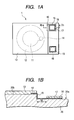
- Fig. 1 is a diaphragm illustrating a capacitive pressure sensor according to an embodiment of the invention, where Fig. 1A is a plan view and Fig. 1B is a sectional view taken along Line Ib-Ib of Fig. 1A.
- the capacitive pressure sensor 1 as shown in Fig. 1A is formed by bonding a glass electrode 20 having a fixed electrode 11 and a silicon substrate 13 having a diaphragm which is a movable electrode.
- a cavity 12 which is a movable area of the diaphragm is formed between the glass substrate 20 and the silicon substrate 13.
- an electrode pad 17 which is an extraction electrode of the movable electrode and an electrode pad 19 which is the extraction electrode of the extraction electrode 11 are formed.
- the electrode pad 17 for the movable electrode is connected electrically to the silicon substrate 13 having the movable electrode with a contact layer 15 interposed therebetween.
- the electrode pad 19 for the fixed electrode is connected to the fixed electrode 11 with a contact pins 14 and 18 interposed therebetween.
- Fig. 1B is a diagram illustrating a connection state between the silicon substrate 13 having the movable electrode and the electrode pad 17 for the movable electrode.
- the glass substrate 20 includes an electrode formation area 20a forming the electrode pad 17 and a bonded area 20b bonding the silicon substrate 13.
- a bump is provided to the glass substrate 20 and the bonded area 20b is provided to a high position, and the electrode formation area 20a is provided to a lower position.
- the configuration may not be limited thereto.
- a contact layer 15 extends from the electrode formation area 20a to the bonded area 20b. Accordingly, the contact layer 15 is bonded to the silicon substrate 13 in the bonded area 20b and the electrode pad 17 is formed on the electrode formation area 20a in an upper part. Accordingly, the silicon substrate 13 having the movable electrode is connected electrically to the electrode pad 17 with the contact layer 15 interposed therebetween.
- the contact layer 15 is formed of a metal which has a good adhesion with glass such as Ti, Cu, Cr, and so on and scatters to the silicon.
- a thickness of the contact layer 15 is in the range of 100 nm to 300 nm by considering an electric conduction characteristic, a gold-silicon eutectic reaction, and an anode bonding characteristic, and so on.
- the silicon substrate 13 is formed on the glass substrate 20 with the contact layer 15 interposed therebetween in the bonded area 20b.
- the gold-silicon eutectic crystal layer 16' is formed on the contact layer 15.
- the gold-silicon eutectic crystal layer 16' can be obtained at the time of bonding the silicon substrate 13 and the glass substrate 20. For example, in parallel with the anode bonding, the eutectic reaction by a gold of the gold-seed layer 16 formed on the contact layer 15 and a silicon of the silicon substrate 13 effect the gold silicon eutectic silicon.
- the gold-silicon eutectic crystal layer 16' serves to prevent an oxidation in a surface of the contact layer 15.
- the gold-silicon eutectic crystal layer 16' is interposed between the contact layer 15 and the silicon substrate 13, that is, since the contact layer 15 and the silicon substrate 13 are connected electrically to each other by using a gold-silicon eutectic reaction at the time of bonding the silicon substrate 13 and the glass substrate 20, a contact resistance between the contact layer 15 and the silicon substrate 13 can be stabilized, a Q value of the sensor can be stabilized, and the satisfactory sensor characteristic can be performed.
- the contact layer 15 and the silicon substrate 13 are bonded to each other by the gold-silicon eutectic reaction, the bonding strength is sufficient.
- the gold-seed layer 16 is formed on the contact layer 15 of the electrode formation area 20a.
- the gold-seed layer 16 is formed in a state where the gold-silicon eutectic crystal layer 16' is separated from the gold-seed layer 16. Since the gold-seed layer 16 does not affect the gold-silicon eutectic crystal layer in the bonded area, it is preferable that the gold-seed layer 16 and the gold-silicon eutectic crystal layer 16' are to be separated from each other by a sufficient distance W.
- the distance W is in the range of 10 ⁇ m to 200 ⁇ m. It is possible to prevent the gold-seed layer 16 from being affected by the gold-silicon eutectic reaction in the bonded area.
- the gold-seed layer 16 serves as a plating seed layer.
- a material forming the seed layer can be varied appropriately by the material forming the electrode pad on the seed layer by considering the contact resistance.
- An electrode pad 17 is formed on the gold-seed layer 16.
- the electrode pad 17 can be connected to an external circuit electrically by connecting means such as a wire bonding, and so on. Forming the electrode pad 17 is determined appropriately depending upon the materials forming the seed layer for materials forming the electrode pad 17.
- the structure of the electrode formation area the structure is not limited to it, but may be changed in various forms.
- an interface between the silicon substrate 13 and the glass substrate 20 has the high adhesion.
- the adhesion can be increased between the substrates 13 and 20 by mounting the silicon substrate 13 in the anode bonding manner on a bonded surface of the glass substrate 20. Accordingly, airtightness in the cavity 12 can be enhanced by exhibiting the high adhesion on the interface between the glass substrate 20 and the silicon substrate 13.
- an anode bond process is a process that a big electrostatic attraction between the silicon and the glass is emitted by applying a predetermined voltage (for example, 300 V ⁇ 1 kV) in a predetermined temperature (for example, 400°C or less), a chemistry bond that an oxygen is interposed between on a contacted glass-silicon interface is formed, or a covalent bond that the oxygen is emitted is formed.
- the covalent bond on the interface is a Si-Si bond or a Si-O bond which is included in a Si atom of the silicon and the glass between Si atoms.
- a glass material of the glass substrate 20 includes an alkali metal such as sodium, and the like (e.g. Pyrex glass (Registered Trademark of corning Corporation)).
- the capacitive pressure sensor having such a configuration includes a predetermined electrostatic capacitance between the diaphragm which is the movable electrode and the fixed electrode 11.
- the diaphragm When pressure is applied to the pressure sensor, the diaphragm is movable by the pressure. Accordingly, the diaphragm is shifted.
- the electrostatic capacitance between the diaphragm and the fixed electrode 11 varies. Accordingly, the variation can be converted into a pressure variation by using the electrostatic capacitance as a parameter.
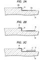
- FIGs. 2A to 2C are sectional views illustrating the method of manufacturing the capacitive pressure sensor according to the first embodiment.
- a recess portion is formed in the buried substrate for the cavity and the fixed electrode is formed.
- a protrusion portion is formed by etching a main one direction of the silicon substrate which is subjected to a low resistance.
- the glass substrate is placed in the protrusion portion, the silicon substrate or the glass substrate is heated in a vacuum, the silicon substrate is pressed on the glass substrate, the protrusion portion is pressed into the glass substrate, and then the silicon substrate and the glass substrate are bonded to each other.
- the buried substrate is manufactured in which the conductive portion is buried in the glass substrate. Then, the fixed electrode is formed by forming the recess portion for the cavity in the buried substrate.
- the contact layer 15 is formed along the bump. Accordingly, a resist film is formed on the glass substrate 20 and the resist film is patterned to open the contact layer formation area. A material forming the contact layer 15 is deposited by a sputtering technique, and so on and then the resist film is removed(lift off).
- the gold -seed layer 16 is formed in a state where the gold-seed layer 16 is separated from the contact layer 15.
- the resist film is formed in the area including the contact layer 15, the resist film is patterned to open the gold-seed layer formation area.
- the material forming the gold-seed layer 16 is deposited by the sputtering technique, and so on and accordingly the resist film is removed (lift off). According to this, the electrode pad 17 is formed on the gold-seed layer 16 by the plating.
- an electrode pad 17 is formed on a gold-seed layer 16.
- a mask is provided on an area around the electrode pad formation area and only the electrode pad formation area is plated to form an electrode pad 17.
- a condition of the plating is generally used condition although the condition may be varied according to material. Accordingly, the resist film is formed on the whole surface and patterned (photo-lithography) so that the resist film can be remained around the electrode pad. Accordingly, the resist film is employed as the mask to etch the gold-seed layer 16 and the contact layer 15. Accordingly, the remaining resist film is removed.
- a silicon substrate 13 which is formed in a predetermined thickness of several tens of micrometers by the etching or the grinding in advance, is bonded on the glass substrate 20 by allowing the diaphragm which is the movable electrode to be placed at an interval of a predetermined gap. Accordingly, the anode bonding process is carried out by applying voltage of about 500 V to the silicon substrate 13 and the glass substrate 20 and heating the substrates under the temperature of 400°C or less. The adhesion at the interface between the silicon substrate 13 and the glass substrate 20 is increased so that the airtightness of the cavity 12 can be improved.
- the capacitive pressure sensor can be obtained.
- the fixed electrode 11 is connected electrically to the electrode pad 19 with contact pins 14 and pin 18 interposed therebetween and the diaphragm is connected electrically to the electrode pad 17 with the contact layer 15 interposed therebetween. Accordingly, the signal of variation of the electrostatic capacitance, which is sensed between the diaphragm and the fixed electrode 11, can be obtained from the electrodes pad 17 and pad 19. Based on this signal, measurement pressure can be calculated.
- the gold-silicon eutectic crystal layer 16' is interposed between the contact layer 15 and the silicon substrate 13, that is, since the contact layer 15 and the silicon substrate 13 are connected electrically to each other by using a gold-silicon eutectic reaction at the time of bonding the silicon substrate 13 and the glass substrate 20, a contact resistance between the contact layer 15 and the silicon substrate 13 can be stabilized, a Q value of the sensor can be stabilized, and the satisfactory sensor characteristic can be performed.
- the contact layer 15 and the silicon substrate 13 are bonded to each other by the gold-silicon eutectic reaction, the bonding strength is sufficient.
- the extraction electrode between the silicon substrate 13 having the diaphragm and the bonded area 20b does not exist, the bonding reliability between the diaphragm and the glass substrate 20 is improved, and the airtightness of the cavity 12 can be increased.
- a two-week promotion test (a pressure cooker test) is performed under the conditions of 100%RH, 2atm (2026hPa) pressure, 121°C.
- the contact resistance in the bonded area is several ⁇ s, which is sufficiently low.
- Fig. 3 is a sectional view showing the schematic configuration of the capacitive pressure sensor according to a second embodiment of the present invention.
- the same elements as Fig. 1B are denoted by the same reference numerals as Fig. 1B and detailed description thereof will be omitted.
- the bonded area 20b has a recess portion 20c and a contact layer 15 is formed in the recess portion 20c.
- a thickness by the contact layer 15 can be accepted in the glass substrate 20, the silicon substrate 13 and the glass substrate 20 are bonded to each other well.
- a depth D of the recess portion 20c is set so that the glass substrate 20 and the contact layer 15 are flush with each other when the contact layer 15 is formed in the recess portion 20c.
- the bonded area between the glass substrate 20 and the contact layer 15 can be flat, only a gold-seed layer 16 contributing to the gold-silicon eutectic crystal reaction can be allowed to protrude and accordingly the gold-silicon eutectic crystal reaction can be embodied surely. As a result, a bonding strength between the silicon substrate 13 and the glass substrate 20 can be increased.
- FIGs. 4A to 4D are cross-sectional illustrating the manufacturing method of the capacitive pressure sensor according to the second embodiment of the invention.
- a buried substrate is provided, the recess portion for a cavity is formed in the buried substrate and a fixed electrode is formed.
- the recess portion 20c for the contact layer 15 is formed on the bonded area 20b of the glass substrate 20.
- a resist film is formed on the glass substrate 20 and patterned so that the resist film can be remained on an area around the recess portion formation area. Accordingly, the resist film is employed as a mask and a milling process is performed in the glass substrate 20. Thereafter, the remaining resist film is removed (lift-off).
- the contact layer 15 is formed from the electrode formation area 20a of the glass substrate 20 to the recess portion 20c of the bonded area 20b.
- the resist film is formed on the glass substrate 20 and patterned to open the contact layer formation area. Accordingly, the material forming the contact layer 15 is deposited by the sputtering technique and accordingly the resist film is removed.
- a gold-seed layer 16 is formed in a state where the gold-seed layer is separated from the contact layer 15.
- the resist film is formed in the area including the contact layer 15, the resist film is patterned to open the gold-seed layer formation area, the material (gold) forming the gold-seed layer 16 is deposited by sputtering technique and the like, and accordingly the resist film is removed (lift-off) . Therefore, an electrode pad 17 can be formed on the gold-seed layer 16 by plating.
- the electrode pad 17 is formed on the gold-seed layer 16.
- the mask is provided in the area around the electrode pad formation area and the electrode pad 17 is formed by performing the only electrode pad formation area.
- the condition of the plating is generally used condition although it may be varied according to the material. Accordingly, the resist film is formed on the whole surface and patterned (photo-lithography) so that the resist film can be remained around the electrode pad. Accordingly, the resist film is employed as a mask to etch the gold-seed layer 16 and the contact layer 15. Thereafter, the remaining resist film is removed.
- a silicon substrate 13 which is formed in a predetermined thickness of several tens micrometers by the etching or the grinding in advance is bonded on the glass substrate 20 by allowing the diaphragm which is the movable electrode to be placed at an interval of a predetermined gap. Accordingly, the anode bonding process is carried out by applying voltage of about 500 V to the silicon substrate 13 and the glass substrate 20 and heating the substrates under the temperature of 400°C or less. The adhesion at the interface between the silicon substrate 13 and the glass substrate 20 is increased so that the airtightness of the cavity 12 can be improved.
- the capacitive pressure sensor can be obtained.
- the fixed electrode 11 is connected electrically to the electrode pad 19 with contact pins 14 and pin 18 interposed therebetween and the diaphragm is connected electrically to the electrode pad 17 with the contact layer 15 interposed therebetween. Accordingly, the signal of variation of the electrostatic capacitance, which is sensed between the diaphragm and the fixed electrode 11, can be obtained from the electrodes pad 17 and pad 19. Based on this signal, measurement pressure can be calculated.
- the gold-silicon eutectic crystal layer 16' is interposed between the contact layer 15 and the silicon substrate 13, that is, since the contact layer 15 and the silicon substrate 13 are connected electrically to each other by using a gold-silicon eutectic reaction at the time of bonding the silicon substrate 13 and the glass substrate 20, a contact resistance between the contact layer 15 and the silicon substrate 13 can be stabilized, a Q value of the sensor can be stabilized, and the satisfactory sensor characteristic can be performed.
- the contact layer 15 and the silicon substrate 13 are bonded to each other by the gold-silicon eutectic reaction, the bonding strength is sufficient.
- the extraction electrode between the silicon substrate 13 having the diaphragm and the bonded area 20b does not exist, the bonding reliability between the diaphragm and the glass substrate 20 is improved, and the airtightness of the cavity 12 can be increased.
- Fig. 6 is a cross-sectional view illustrating the schematic configuration of a capacitive pressure sensor according to the second embodiment of the invention.
- the same elements as shown in Figs. 1A and 1B are denoted by the same reference numerals as shown in Figs. 1A and 1B and detailed description thereof will be omitted.
- the recess portion 20c is formed in the bonded area 20c of the glass substrate 20 and the contact layer 15 extends from the recess portion 20c to the electrode formation area20a. Accordingly, the contact layer 15 is bonded to the silicon substrate 13 on the bonded area 20b and the electrode pad 17 is formed on the electrode formation area 20a in an upper part.
- the silicon substrate 13 having the movable electrode is connected electrically to the electrode pad 17 with the contact layer 15 interposed therebetween.
- the contact layer 15 is formed of a metal which has a good adhesion with glass such as Ti, Cu, Cr, TiAu, TiTa and so on and scatters to the silicon.
- a thickness of the contact layer 15 is in the range of 100 nm to 300 nm by considering an electric conduction characteristic, a gold-silicon eutectic reaction, and an anode junction characteristic, and so on.
- the silicon substrate 13 is formed on the glass substrate 20 with the contact layer 15 interposed therebetween in the bonded area 20b.
- the gold-silicon eutectic crystal layer 16' is formed on the contact layer 15.
- the gold-silicon eutectic crystal layer 16' can be obtained at the time of bonding the silicon substrate 13 and the glass substrate 20. For example, in parallel with the anode bonding the eutectic reaction by a gold of the gold-seed layer 16 formed on the contact layer 15 and a silicon of the silicon substrate 13 effect the gold silicon eutectic silicon.
- the gold-silicon eutectic crystal layer 16' serves to prevent an oxidation in a surface of the contact layer 15.
- the contact layer 15 protrudes from a position of the surface of the glass substrate 20 in the bonded area 20b. Due to the protrusion of the contact layer 15 from the surface of the glass substrate 20, when the glass substrate 20 and the silicon substrate 13 are pressed and bonded to each other, the gold-seed layer and the silicon substrate 13 are contacted surely and the gold-silicon eutectic crystal reaction of the both things can be easily performed between both things. That is, when the glass substrate 20 is bonded to the silicon substrate 13, by preventing a gap between the gold of the gold-seed layer and the silicon substrate 13, so it can contribute to the gold-silicon eutectic crystal reaction efficiently.
- the protrusion height h of the contact layer 15 is about 3,000 ⁇ or less, preferably in the range of 300 ⁇ to 3,000 ⁇ .
- the gold-silicon eutectic crystal layer 16' is interposed between the contact layer 15 and the silicon substrate 13, that is, since the contact layer 15 and the silicon substrate 13 are connected electrically to each other by using a gold-silicon eutectic reaction at the time of bonding the silicon substrate 13 and the glass substrate 20, a contact resistance between the contact layer 15 and the silicon substrate 13 can be stabilized, a Q value of the sensor can be stabilized, and the satisfactory sensor characteristic can be performed.
- the contact layer 15 and the silicon substrate 13 are bonded to each other by the gold-silicon eutectic reaction, the bonding strength is sufficient.
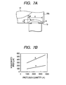
- a non-bonded area A is created between the glass substrate 20 and the silicon substrate 13 near the contact layer 15.
- the distance W from an outer end portion of the non-bonded area A to the end portion of the cavity 12 is about 150 ⁇ m or more, preferably in the range of 150 ⁇ m to 310 ⁇ m.
- the bonding between the silicon substrate 13 and the glass substrate 20 is sufficient, the movable electrode is sufficiently varied by the pressure, and accordingly the sensor operated as the sensor.
- the protrusion height h of the contact layer 15 increases, the distance W from the outer end portion of the non-bonded area A to the end portion of a cavity 12 decreases. Accordingly, the inventors noticed that when the protrusion height h of the contact layer 15 and distance W are optimized, the bonding between the glass substrate 20 and the silicon substrate 13 are made sufficiently, which became the motive of conceiving the present invention. In other words, the objection of the present invention is that the bonding of substrates can be ensured by optimizing the protrusion height h of the contact layer 15 and distance W even when the extraction electrode exists between substrates in the bonded area, thereby performing the satisfactory sensor characteristic.
- the gold-seed layer 16 is formed on the contact layer 15 of the electrode formation area 20a.
- the gold-seed layer 16 serves as a plating seed layer.
- a material forming the seed layer can be varied appropriately by the material forming the electrode pad on the seed layer by considering the contact resistance.
- An electrode pad 17 is formed on the gold-seed layer 16.
- the electrode pad 17 can be connected to an external circuit electrically by connecting means such as a wire bonding, and so on. Forming the electrode pad 17 is determined appropriately depending upon the materials forming the seed layer for materials forming the electrode pad 17.
- the structure of the electrode formation area the structure is not limited to it, but may be changed in various forms.
- an interface between the silicon substrate 13 and the glass substrate 20 has the high adhesion.
- the adhesion can be increased between the substrates 13 and 20 by mounting the silicon substrate 13 in the anode bonding manner on a bonded surface of the glass substrate 20. Accordingly, airtightness in the cavity 12 can be enhanced by exhibiting the high adhesion on the interface between the glass substrate 20 and the silicon substrate 13.
- an anode bond process is a process that a big electrostatic attraction between the silicon and the glass is emitted by applying a predetermined voltage (for example, 300 V ⁇ 1 kV) in a predetermined temperature (for example, 400°C or less), a chemistry bond that an oxygen is interposed between on a contacted glass-silicon interface is formed, or a covalent bond that the oxygen is emitted is formed.
- the covalent bond on the interface is a Si-Si bond or a Si-O bond which is included in a Si atom of the silicon and the glass between Si atoms.
- a glass material of the glass substrate 20 includes an alkali metal such as sodium, and the like (e.g. Pyrex glass (Registered Trademark of corning Corporation)).
- the capacitive pressure sensor having such a configuration includes a predetermined electrostatic capacitance between the diaphragm which is the movable electrode and the fixed electrode 11.
- the diaphragm When pressure is applied to the pressure sensor, the diaphragm is movable by the pressure. Accordingly, the diaphragm is shifted.
- the electrostatic capacitance between the diaphragm and the fixed electrode 11 varies. Accordingly, the variation can be converted into a pressure variation by using the electrostatic capacitance as a parameter.
- FIGs. 2A to 2C are sectional views illustrating the method of manufacturing the capacitive pressure sensor according to the first embodiment.
- a recess portion is formed in the buried substrate for the cavity and the fixed electrode is formed.
- a protrusion portion is formed by etching a main one direction of the silicon substrate which is subjected to a low resistance.
- the glass substrate is placed in the protrusion portion, the silicon substrate or the glass substrate is heated in a vacuum, the silicon substrate is pressed on the glass substrate, the protrusion portion is pressed into the glass substrate, and then the silicon substrate and the glass substrate are bonded to each other.
- the buried substrate is manufactured in which the conductive portion is buried in the glass substrate. Then, the fixed electrode is formed by forming the recess portion for the cavity in the buried substrate.
- the recess portion 20c for a contact layer 15 is formed in the bonded area 20b of the glass substrate 20.
- the resist film is formed on the glass substrate 20 and patterned so that the resist film can be remained on the area around the recess portion formation area. Then, the resist film is employed as a mask and a milling process is performed for the glass substrate 20. Thereafter, the remaining resist film is removed.
- the height of the contact layer 15 protruding from the surface of the glass substrate 20 is about 3000 ⁇ or less.
- the contact layer 15 is formed along the bump. Accordingly, a resist film is formed on the glass substrate 20 and the resist film is patterned to open the contact layer formation area. A material forming the contact layer 15 is deposited by a sputtering technique, and so on and accordingly the resist film is removed (lift off).
- the gold -seed layer 16 is formed in a state where the gold-seed layer 16 is separated from the contact layer 15.
- the resist film is formed in the area including the contact layer 15 and the resist film is patterned to open the gold-seed layer formation area.
- the material forming the gold-seed layer 16 is deposited by the sputtering technique, and so on and accordingly the resist film is removed (lift off). Accordingly, the electrode pad 17 is formed on the gold-seed layer 16 by the plating.
- an electrode pad 17 is formed on a gold-seed layer 16.
- a mask is provided on an area around the electrode pad formation area and only the electrode pad formation area is plated to form an electrode pad 17.
- a condition of the plating is generally used condition although the condition may be varied according to material. Accordingly, the resist film is formed on the whole surface and patterned (photo-lithography) so that the resist film can be remained around the electrode pad. Accordingly, the resist film is employed as the mask to etch the gold-seed layer 16 and the contact layer 15. Accordingly, the remaining resist film is removed.
- a silicon substrate 13 which is formed in a predetermined thickness of several tens of micrometers by the etching or the grinding in advance is bonded on the glass substrate 20 by allowing the diaphragm which is the movable electrode to be placed at an interval of a predetermined gap. Accordingly, the anode bonding process is carried out by applying voltage of about 500 V to the silicon substrate 13 and the glass substrate 20 and heating the substrates under the temperature of 400°C or less. The adhesion at the interface between the silicon substrate 13 and the glass substrate 20 is increased so that the airtightness of the cavity 12 can be improved.
- the capacitive pressure sensor can be obtained.
- a distance from the outer end portion of the non-bonded area A in the bonded area 20b to the end of the cavity 12 is about 150 ⁇ m or more.
- the fixed electrode 11 is connected electrically to the electrode pad 19 with contact pins 14 and pin 18 interposed therebetween and the diaphragm is connected electrically to the electrode pad 17 with the contact layer 15 interposed therebetween. Accordingly, the signal of variation of the electrostatic capacitance, which is sensed between the diaphragm and the fixed electrode 11, can be obtained from the electrodes pad 17 and pad 19. Based on this signal, measurement pressure can be calculated.
- the capacitive pressure sensor optimizes the protrusion height h of the contact layer 15 in the bonded area 20b and the distance W from the outer end portion of the non-bonded area A in the bonded area 20 b to the end portion of the cavity 12. That is, since the distance W from the outer end of the non-bonded area A existing in the bonded area 20b to the end portion of the cavity 12 is about 150 ⁇ m or more and the protrusion height h of the contact layer from the surface of the glass substrate 20 is about 3,000 ⁇ or less, the substrates are bonded surely even when the existence of the extraction electrode existed in the bonded area between substrates, thereby performing a satisfactory sensor characteristic.
- the gold-silicon eutectic crystal layer 16' is interposed between the contact layer 15 and the silicon substrate 13, that is, since the contact layer 15 and the silicon substrate 13 are connected electrically to each other by using a gold-silicon eutectic reaction at the time of bonding the silicon substrate 13 and the glass substrate 20, a contact resistance between the contact layer 15 and the silicon substrate 13 can be stabilized, a Q value of the sensor can be stabilized, and the satisfactory sensor characteristic can be performed.
- the contact layer 15 and the silicon substrate 13 are bonded to each other by the gold-silicon eutectic reaction, the bonding strength is sufficient.
- the extraction electrode between the silicon substrate 13 having the diaphragm and the bonded area 20b does not exist, the bonding reliability between the diaphragm and the glass substrate 20 is improved, and the airtightness of the cavity 12 can be increased.
- the optimization values of the protrusion height h of the contact layer 15 in the bonded area 20 b and the distance W from the outer end portion of the non-bonded area A to the end portion of the cavity 12 will be described.
- a capacity evaluation test before and after reliability test and ESR (equivalent serial resistor) evaluation are carried out. The results will be shown in a table 1 below.
- the sealing width (W) is 60 ⁇ m, 100 ⁇ m, 120 ⁇ m, 150 ⁇ m, 250 ⁇ m, 285 ⁇ m, 310 ⁇ m, and 330 ⁇ m respectively. Also, each evaluation was performed for 10 samples of each type of the capacity pressure sensor.
- the capacitance evaluation was performed by examining whether or not there is any variation in electrostatic capacitance by applying pressure 1 ⁇ 5 Pa (100 kPa ⁇ 500kPa) to a capacitive pressure sensor by using a LCR meter 4275A (Registered Trademark of Agilent Technology Corporation).
- pressure 1 ⁇ 5 Pa 100 kPa ⁇ 500kPa
- LCR meter 4275A Registered Trademark of Agilent Technology Corporation.
- the case where there is any change in every 10 sample is marked by ⁇ ; the case where there is any change in 8 samples or more is marked by O; and other cases are marked by X.
- the ESR evaluation was performed by examining resistances except the capacitance and the inductance by using the LCR meter 4185A (Registered Trade Mark of Agilent Technology Corporation). The case where 10 samples have ESR of 4 ⁇ or less is marked by ⁇ , the case where 8 samples have ESR of 4 ⁇ or less is marked by o, and the other cases are marked by X.
- the optimization values of the protrusion height h of the contact layer 15 in the bonded area 20 b and the distance W from the outer end portion of the non-bonded area A to the end portion of the cavity 12 in the bonded area 20b are as follows: a protrusion height (h) is about 3,000 ⁇ or less; and a sealing width (W) is about 150 ⁇ m or more.
- a protrusion height (h) is about 3,000 ⁇ or less
- a sealing width (W) is about 150 ⁇ m or more.
- the ESR of the samples having the protrusion heights of 4200 ⁇ and 3800 ⁇ is x, because a connection failure, a broken wire, or a corrosion occurs due to breakage of the sealing of the cavity 12.
- the cavity 12 could be sealed.
- the present invention is not limited only to embodiments 1, 2 and 3 but various modifications are possible.
- the structure and configuration of the capacitive pressure sensor only when it is made by the bonding of the glass substrate having the fixed electrode and the silicon substrate having the movable electrode.
- etching or milling process is performed with the generally used conditions in the embodiments 1, 2 and 3.
- the processes are not limited only to the above-mentioned ones in the embodiments 1, 2 and 3 but proper exchange of an order is possible between the processes.
- Other modifications are also possible without departing from the scope of the objection of the present invention.
- the present invention can be applied, for example, to a barometer monitoring an atmospheric pressure or a capacitive pressure sensor monitoring gas pressure.
Landscapes
- Physics & Mathematics (AREA)
- General Physics & Mathematics (AREA)
- Chemical & Material Sciences (AREA)
- Engineering & Computer Science (AREA)
- Ceramic Engineering (AREA)
- Measuring Fluid Pressure (AREA)
- Pressure Sensors (AREA)
Abstract
Description
- The present invention relates to a pressure sensor for sensing pressure, and more particularly, to a capacitive pressure sensor for sensing pressure by using electrostatic capacitance.
- A capacitive pressure sensor is formed by bonding a substrate having a pressure-sensitive diaphragm which is a movable electrode and a substrate having a fixed electrode to each other with a gap (cavity) between the pressure-sensitive diaphragm and the fixed electrode. When pressure is applied to the pressure-sensitive diaphragm in the capacitive pressure sensor, the pressure-sensitive diaphragm is deformed and the gap between the pressure-sensitive diaphragm and the fixed electrode is varied. Electrostatic capacitance is varied between the pressure-sensitive diaphragm and the fixed electrode varies with the variation of the gap. Accordingly, a variation in pressure is sensed by using the variation of the electrostatic capacitance.
- For example, in the capacitive pressure sensor, as shown in Fig. 5, a
glass substrate 102 having afixed electrode 103 is disposed on a supportingsubstrate 101. Asilicon substrate 104 having adiaphragm 104a is bonded to theglass substrate 102. In such a capacitive pressure sensor, since anextraction electrode 105 for thefixed electrode 103 and anextraction electrode 106 for the movable electrode (diaphragm 104a) are patterned on theglass substrate 102, the extraction electrodes are disposed in a bonded area between theglass substrate 102 and thesilicon substrate 104 disclosed. An example of such a capacitive pressure sensor is disclosed inJP-A-8-75582 - However, in such a structure, the
extraction electrodes glass substrate 102 and thesilicon substrate 104. Accordingly, in theextraction electrode glass substrate 102 and thesilicon substrate 104 are not bonded to each other well, airtightness of the cavity between theglass substrate 102 and thesilicon substrate 104 is not sufficient. As a result, there is a problem that thediaphragm 104a does not serve as the movable electrode and the sensor does not operate accordingly. When theglass substrate 102 and thesilicon substrate 104 are not bonded to each other well in theextraction electrodes - It is an object of the present invention to provide a capacitive pressure sensor capable of exhibiting a satisfactory sensor characteristic with a sufficient bonding strength between substrates even when an extraction electrode exists in a bonded area between the substrates.
- The capacitive pressure sensor includes: a glass substrate having a fixed electrode; a silicon substrate having a movable electrode; a bonded area between the glass substrate and the silicon substrate; an extraction electrode formation area on the glass substrate for the movable electrode; a contact layer extending from the bonded area to the extraction electrode formation area; a gold-silicon eutectic crystal layer provided between the contact layer and the silicon substrate in the bonded area.
- According to the configuration, since the gold-silicon eutectic crystal layer is interposed between the contact layer and the silicon substrate, that is, since the contact layer and the silicon substrate are connected electrically to each other by using a gold-silicon eutectic reaction at the time of bonding the silicon substrate and the glass substrate, a contact resistance between the contact layer and the silicon substrate can be stabilized, a Q value of the sensor can be stabilized, and the satisfactory sensor characteristic can be performed. In addition, since the contact layer and the silicon substrate are bonded to each other by the gold-silicon eutectic reaction, the bonding strength is sufficient.
- In the capacitive pressure sensor of the invention, it preferable that the bonded area has a recess portion and the contact layer is formed on the recess portion. According to the configuration, since the glass substrate can absorb a thickness by the contact layer, the silicon substrate and the glass substrate can be bonded to each other well.
- In the capacitive pressure sensor of the invention, a depth of the recess portion is set so that the glass substrate and the contact layer are flush with each other when the contact layer is formed in the recess portion. According to the configuration, since the bonded area between the glass substrate and the contact layer can be flat and only a gold layer which is contributing to a gold-silicon eutectic crystal reaction can be allowed to protrude, the gold-silicon eutectic crystal layer reaction can be embodied surely. As a result, the bonding strength between the silicon substrate and the glass substrate can be increased.
- In the capacitive pressure sensor of the invention, it is preferable that the gold layer is formed on the extraction electrode formation area of the contact layer in a state where the gold layer is separated from the gold-silicon eutectic crystal layer. According to the configuration, it is possible to prevent the gold layer from being affected by the gold-silicon eutectic reaction in the bonded area.
- The capacitive pressure sensor includes: the glass substrate having the fixed electrode; the silicon substrate having the movable electrode so as to form a cavity; a bonded area between the glass substrate and the silicon substrate; the extraction electrode formation area on the glass substrate of the movable electrode, the contact layer protruding from the bonded area to the extraction electrode formation area; the gold-silicon eutectic crystal layer provided between the contact layer and the silicon substrate in the bonded area. A distance from an outer end portion of a non-bonded area which is formed in the bonded area to an end portion of the cavity is 150 µm or more and a height of the contact layer protruding from a surface of the glass substrate is 3000 Å or less.
- According to the configuration, since the distance from the outer end portion of the non-bonded area which is formed in the bonded area between the glass substrate and the silicon substrate to an end portion of the cavity is 150 µm or more, the glass substrate and the silicon substrate are bonded to each other well, thereby providing an excellent sensor. Since the height of the contact layer protruding from the surface of the glass substrate is 3000 Å or less in the bonded area, the silicon substrate and the glass substrate are bonded to each other well, the movable electrode varies sufficiently by pressure, and accordingly the sensor operates as a sensor. For this case, since the gold-silicon eutectic reaction is performed sufficiently at the time of bonding the silicon substrate and the glass substrate, a contact resistor between the contact layer and the silicon substrate is stabilized, accordingly the Q value of the sensor is stabilized and the satisfactory sensor characteristic can be exhibited. Since the contact layer and the silicon substrate are bonded by the gold-silicon eutectic reaction, the bonding strength is sufficient.
- In the capacitive pressure sensor of the invention, it preferable that the bonded area has the recess portion and the contact layer is formed on the recess portion. According to the configuration, since the glass substrate can absorb a thickness by the contact layer, the silicon substrate and the glass substrate can be bonded to each other well.
- In the capacitive pressure sensor of the invention, it is preferable that an interface between the glass substrate and the silicon substrate has one of a Si-Si bond or a Si-O bond. According to the configuration, since the silicon and the glass are bonded to each other well and the interface of both things exhibits a high adhesion, airtightness in the cavity can be improved.
- According to the capacitive pressure sensor of the invention, the capacitive pressure sensor which is formed by bonding the glass substrate having the fixed electrode and the silicon substrate having the movable electrode, in which the silicon substrate includes the extraction electrode formation area for the movable electrode, includes the contact layer extending from the bonded area between the glass substrate and the silicon substrate to the extraction electrode formation area and the gold-silicon eutectic crystal layer provided between the contact layer and the silicon substrate in the bonded area. Accordingly, even when the extraction electrode existed in the bonded area between substrates, the bonding strength is sufficient between the substrates and the satisfactory sensor characteristic can be exhibited. The capacitive pressure sensor of the invention which is formed by bonding the glass substrate having the fixed electrode and the silicon substrate having the movable electrode so as to form a cavity includes the contact layer protruding from the bonded area between the glass substrate and the silicon substrate and the gold-silicon eutectic crystal layer provided between the contact layer and the silicon substrate in the bonded area. Since the distance from the outer end portion of the non-bonded area which is formed in the bonded area to the end portion of the cavity is 150 µm or more and the height of the contact layer protruding from the plane of the glass substrate is 3000 Å or less, even when the extraction electrode existed in the bonded area between the substrates, the bonding strength is sufficient and the satisfactory sensor characteristic can be performed between the substrates.
-
- Fig. 1 is a schematic view illustrating a configuration of a capacitive pressure sensor according to a first embodiment, where Fig. 1A is a plan view and Fig. 1B is a sectional view taken along Line Ib-Ib of Fig. 1A.
- Figs. 2A to 2C are sectional views illustrating a method of manufacturing a capacitive pressure sensor according to the first embodiment of the invention.
- Fig. 3 is a schematic diagram illustrating a configuration of a capacitive pressure sensor according to a second embodiment of the invention.
- Figs. 4A to 4D are sectional views illustrating a method of manufacturing a capacitive pressure sensor according to the second embodiment of the invention.
- Fig. 5 is a known sectional view illustrating a capacitive pressure sensor.
- Fig. 6 is a schematic diagram showing a configuration of a capacitive pressure sensor, where Fig. 6A is a plan view and Fig. 6B is a sectional view taken along Line IVb-VIb of Fig. 6A according to a third embodiment of the invention.
- Fig. 7A is a diagram illustrating a non-bonded area of a capacitive pressure sensor according to the third embodiment of the invention. Fig. 7B is a diagram illustrating a relation between a thickness of a contact layer and the non-bonded area.
- Figs. 8A to 8D are sectional views illustrating a method of manufacturing a capacitive pressure sensor according to the third embodiment of the invention.
- Hereinafter, embodiments of the invention will be described with the accompanying drawings.
- Fig. 1 is a diaphragm illustrating a capacitive pressure sensor according to an embodiment of the invention, where Fig. 1A is a plan view and Fig. 1B is a sectional view taken along Line Ib-Ib of Fig. 1A.
- The
capacitive pressure sensor 1 as shown in Fig. 1A is formed by bonding aglass electrode 20 having a fixedelectrode 11 and asilicon substrate 13 having a diaphragm which is a movable electrode. Acavity 12 which is a movable area of the diaphragm is formed between theglass substrate 20 and thesilicon substrate 13. - Around the
cavity area 12, anelectrode pad 17 which is an extraction electrode of the movable electrode and anelectrode pad 19 which is the extraction electrode of theextraction electrode 11 are formed. Theelectrode pad 17 for the movable electrode is connected electrically to thesilicon substrate 13 having the movable electrode with acontact layer 15 interposed therebetween. Theelectrode pad 19 for the fixed electrode is connected to the fixedelectrode 11 with a contact pins 14 and 18 interposed therebetween. - Fig. 1B is a diagram illustrating a connection state between the
silicon substrate 13 having the movable electrode and theelectrode pad 17 for the movable electrode. As shown in fig. 1B, theglass substrate 20 includes anelectrode formation area 20a forming theelectrode pad 17 and a bondedarea 20b bonding thesilicon substrate 13. Herein, a bump is provided to theglass substrate 20 and the bondedarea 20b is provided to a high position, and theelectrode formation area 20a is provided to a lower position. However, the configuration may not be limited thereto. - On the
substrate 20, acontact layer 15 extends from theelectrode formation area 20a to the bondedarea 20b. Accordingly, thecontact layer 15 is bonded to thesilicon substrate 13 in the bondedarea 20b and theelectrode pad 17 is formed on theelectrode formation area 20a in an upper part. Accordingly, thesilicon substrate 13 having the movable electrode is connected electrically to theelectrode pad 17 with thecontact layer 15 interposed therebetween. Thecontact layer 15 is formed of a metal which has a good adhesion with glass such as Ti, Cu, Cr, and so on and scatters to the silicon. In addition, it is preferable that a thickness of thecontact layer 15 is in the range of 100 nm to 300 nm by considering an electric conduction characteristic, a gold-silicon eutectic reaction, and an anode bonding characteristic, and so on. - The
silicon substrate 13 is formed on theglass substrate 20 with thecontact layer 15 interposed therebetween in the bondedarea 20b. The gold-silicon eutectic crystal layer 16' is formed on thecontact layer 15. The gold-silicon eutectic crystal layer 16' can be obtained at the time of bonding thesilicon substrate 13 and theglass substrate 20. For example, in parallel with the anode bonding, the eutectic reaction by a gold of the gold-seed layer 16 formed on thecontact layer 15 and a silicon of thesilicon substrate 13 effect the gold silicon eutectic silicon. The gold-silicon eutectic crystal layer 16' serves to prevent an oxidation in a surface of thecontact layer 15. - Accordingly, since the gold-silicon eutectic crystal layer 16' is interposed between the
contact layer 15 and thesilicon substrate 13, that is, since thecontact layer 15 and thesilicon substrate 13 are connected electrically to each other by using a gold-silicon eutectic reaction at the time of bonding thesilicon substrate 13 and theglass substrate 20, a contact resistance between thecontact layer 15 and thesilicon substrate 13 can be stabilized, a Q value of the sensor can be stabilized, and the satisfactory sensor characteristic can be performed. In addition, since thecontact layer 15 and thesilicon substrate 13 are bonded to each other by the gold-silicon eutectic reaction, the bonding strength is sufficient. - The gold-
seed layer 16 is formed on thecontact layer 15 of theelectrode formation area 20a. The gold-seed layer 16 is formed in a state where the gold-silicon eutectic crystal layer 16' is separated from the gold-seed layer 16. Since the gold-seed layer 16 does not affect the gold-silicon eutectic crystal layer in the bonded area, it is preferable that the gold-seed layer 16 and the gold-silicon eutectic crystal layer 16' are to be separated from each other by a sufficient distance W. For example, the distance W is in the range of 10 µm to 200 µm. It is possible to prevent the gold-seed layer 16 from being affected by the gold-silicon eutectic reaction in the bonded area. The gold-seed layer 16 serves as a plating seed layer. A material forming the seed layer can be varied appropriately by the material forming the electrode pad on the seed layer by considering the contact resistance. - An
electrode pad 17 is formed on the gold-seed layer 16. Theelectrode pad 17 can be connected to an external circuit electrically by connecting means such as a wire bonding, and so on. Forming theelectrode pad 17 is determined appropriately depending upon the materials forming the seed layer for materials forming theelectrode pad 17. The structure of the electrode formation area, the structure is not limited to it, but may be changed in various forms. - It is preferable that an interface between the
silicon substrate 13 and theglass substrate 20 has the high adhesion. At the time of bonding thesilicon substrate 13 to theglass substrate 20, the adhesion can be increased between thesubstrates silicon substrate 13 in the anode bonding manner on a bonded surface of theglass substrate 20. Accordingly, airtightness in thecavity 12 can be enhanced by exhibiting the high adhesion on the interface between theglass substrate 20 and thesilicon substrate 13. - Herein, an anode bond process is a process that a big electrostatic attraction between the silicon and the glass is emitted by applying a predetermined voltage (for example, 300 V~1 kV) in a predetermined temperature (for example, 400°C or less), a chemistry bond that an oxygen is interposed between on a contacted glass-silicon interface is formed, or a covalent bond that the oxygen is emitted is formed. The covalent bond on the interface is a Si-Si bond or a Si-O bond which is included in a Si atom of the silicon and the glass between Si atoms. Accordingly, the silicon and the glass are bonded strongly by the Si-Si bond, or the Si-O bond, and a high adhesion is exhibited in the interface of both things with each other. In order to perform such an anode bonding efficiently, it is preferable that a glass material of the
glass substrate 20 includes an alkali metal such as sodium, and the like (e.g. Pyrex glass (Registered Trademark of corning Corporation)). - The capacitive pressure sensor having such a configuration includes a predetermined electrostatic capacitance between the diaphragm which is the movable electrode and the fixed
electrode 11. When pressure is applied to the pressure sensor, the diaphragm is movable by the pressure. Accordingly, the diaphragm is shifted. At this time, the electrostatic capacitance between the diaphragm and the fixedelectrode 11 varies. Accordingly, the variation can be converted into a pressure variation by using the electrostatic capacitance as a parameter. - Next, a method of manufacturing the capacitive pressure sensor of the first embodiment will be described. Figs. 2A to 2C are sectional views illustrating the method of manufacturing the capacitive pressure sensor according to the first embodiment.
- At the time of manufacturing the capacitive pressure sensor according to the embodiment, for example, by manufacturing a buried substrate burying a conductive portion of the silicon to the glass substrate, a recess portion is formed in the buried substrate for the cavity and the fixed electrode is formed. Specifically, a protrusion portion is formed by etching a main one direction of the silicon substrate which is subjected to a low resistance. The glass substrate is placed in the protrusion portion, the silicon substrate or the glass substrate is heated in a vacuum, the silicon substrate is pressed on the glass substrate, the protrusion portion is pressed into the glass substrate, and then the silicon substrate and the glass substrate are bonded to each other. By performing a grinding process of the glass substrate and the silicon substrate and exposing the protrusion portion in both side of the glass substrate, the buried substrate is manufactured in which the conductive portion is buried in the glass substrate. Then, the fixed electrode is formed by forming the recess portion for the cavity in the buried substrate.
- As shown in Fig. 2A, from the
electrode formation area 20a of theglass substrate 20 to the bondedarea 20b, thecontact layer 15 is formed along the bump. Accordingly, a resist film is formed on theglass substrate 20 and the resist film is patterned to open the contact layer formation area. A material forming thecontact layer 15 is deposited by a sputtering technique, and so on and then the resist film is removed(lift off). - Accordingly, as shown in Fig. 2B, the gold -
seed layer 16 is formed in a state where the gold-seed layer 16 is separated from thecontact layer 15. For this case, the resist film is formed in the area including thecontact layer 15, the resist film is patterned to open the gold-seed layer formation area. The material forming the gold-seed layer 16 is deposited by the sputtering technique, and so on and accordingly the resist film is removed (lift off). According to this, theelectrode pad 17 is formed on the gold-seed layer 16 by the plating. - Accordingly, as shown in Fig. 2C, an
electrode pad 17 is formed on a gold-seed layer 16. In this case, a mask is provided on an area around the electrode pad formation area and only the electrode pad formation area is plated to form anelectrode pad 17. Also, a condition of the plating is generally used condition although the condition may be varied according to material. Accordingly, the resist film is formed on the whole surface and patterned (photo-lithography) so that the resist film can be remained around the electrode pad. Accordingly, the resist film is employed as the mask to etch the gold-seed layer 16 and thecontact layer 15. Accordingly, the remaining resist film is removed. - Accordingly, a
silicon substrate 13 which is formed in a predetermined thickness of several tens of micrometers by the etching or the grinding in advance, is bonded on theglass substrate 20 by allowing the diaphragm which is the movable electrode to be placed at an interval of a predetermined gap. Accordingly, the anode bonding process is carried out by applying voltage of about 500 V to thesilicon substrate 13 and theglass substrate 20 and heating the substrates under the temperature of 400°C or less. The adhesion at the interface between thesilicon substrate 13 and theglass substrate 20 is increased so that the airtightness of thecavity 12 can be improved. Accordingly, for the gold-seed layer 16 between thecontact layer 15 and thesilicon substrate 13 in the bondedarea 20b, by the gold-silicon eutectic reaction of the gold of the gold-seed layer 16 and the silicon of thesilicon substrate 13 is converted into the gold-silicon eutectic crystal layer 16'. Accordingly, the capacitive pressure sensor can be obtained. - In the capacitive pressure sensor, which has been obtained from the above-mentioned process, the fixed
electrode 11 is connected electrically to theelectrode pad 19 with contact pins 14 andpin 18 interposed therebetween and the diaphragm is connected electrically to theelectrode pad 17 with thecontact layer 15 interposed therebetween. Accordingly, the signal of variation of the electrostatic capacitance, which is sensed between the diaphragm and the fixedelectrode 11, can be obtained from theelectrodes pad 17 andpad 19. Based on this signal, measurement pressure can be calculated. - Accordingly, since the gold-silicon eutectic crystal layer 16' is interposed between the
contact layer 15 and thesilicon substrate 13, that is, since thecontact layer 15 and thesilicon substrate 13 are connected electrically to each other by using a gold-silicon eutectic reaction at the time of bonding thesilicon substrate 13 and theglass substrate 20, a contact resistance between thecontact layer 15 and thesilicon substrate 13 can be stabilized, a Q value of the sensor can be stabilized, and the satisfactory sensor characteristic can be performed. In addition, since thecontact layer 15 and thesilicon substrate 13 are bonded to each other by the gold-silicon eutectic reaction, the bonding strength is sufficient. Also, since the extraction electrode between thesilicon substrate 13 having the diaphragm and the bondedarea 20b does not exist, the bonding reliability between the diaphragm and theglass substrate 20 is improved, and the airtightness of thecavity 12 can be increased. - For the capacitive pressure sensor, which has been obtained from the above-mentioned process, a two-week promotion test (a pressure cooker test) is performed under the conditions of 100%RH, 2atm (2026hPa) pressure, 121°C. As a result, the contact resistance in the bonded area is several Ωs, which is sufficiently low.
- Fig. 3 is a sectional view showing the schematic configuration of the capacitive pressure sensor according to a second embodiment of the present invention. In Fig. 3, the same elements as Fig. 1B are denoted by the same reference numerals as Fig. 1B and detailed description thereof will be omitted.
- In the capacitive pressure sensor as shown in Fig. 3, the bonded
area 20b has arecess portion 20c and acontact layer 15 is formed in therecess portion 20c. According to the configuration, a thickness by thecontact layer 15 can be accepted in theglass substrate 20, thesilicon substrate 13 and theglass substrate 20 are bonded to each other well. Specifically, a depth D of therecess portion 20c is set so that theglass substrate 20 and thecontact layer 15 are flush with each other when thecontact layer 15 is formed in therecess portion 20c. Accordingly, since the bonded area between theglass substrate 20 and thecontact layer 15 can be flat, only a gold-seed layer 16 contributing to the gold-silicon eutectic crystal reaction can be allowed to protrude and accordingly the gold-silicon eutectic crystal reaction can be embodied surely. As a result, a bonding strength between thesilicon substrate 13 and theglass substrate 20 can be increased. - Hereinafter, a manufacturing method of the capacitive pressure sensor according to the second embodiment of the invention will be described. Figs. 4A to 4D are cross-sectional illustrating the manufacturing method of the capacitive pressure sensor according to the second embodiment of the invention.
- At the time of manufacturing the capacitive pressure sensor according to the embodiment, identically with the first embodiment, a buried substrate is provided, the recess portion for a cavity is formed in the buried substrate and a fixed electrode is formed.
- Accordingly, as shown in Fig. 4A, the
recess portion 20c for thecontact layer 15 is formed on the bondedarea 20b of theglass substrate 20. In this case, a resist film is formed on theglass substrate 20 and patterned so that the resist film can be remained on an area around the recess portion formation area. Accordingly, the resist film is employed as a mask and a milling process is performed in theglass substrate 20. Thereafter, the remaining resist film is removed (lift-off). - Accordingly, as shown in Fig. 4B, the
contact layer 15 is formed from theelectrode formation area 20a of theglass substrate 20 to therecess portion 20c of the bondedarea 20b. In this case, the resist film is formed on theglass substrate 20 and patterned to open the contact layer formation area. Accordingly, the material forming thecontact layer 15 is deposited by the sputtering technique and accordingly the resist film is removed. - Accordingly, as shown in Fig. 4C, a gold-
seed layer 16 is formed in a state where the gold-seed layer is separated from thecontact layer 15. In this case, the resist film is formed in the area including thecontact layer 15, the resist film is patterned to open the gold-seed layer formation area, the material (gold) forming the gold-seed layer 16 is deposited by sputtering technique and the like, and accordingly the resist film is removed (lift-off) . Therefore, anelectrode pad 17 can be formed on the gold-seed layer 16 by plating. - Accordingly, as shown in Fig. 4D, the
electrode pad 17 is formed on the gold-seed layer 16. In this case, the mask is provided in the area around the electrode pad formation area and theelectrode pad 17 is formed by performing the only electrode pad formation area. Also, the condition of the plating is generally used condition although it may be varied according to the material. Accordingly, the resist film is formed on the whole surface and patterned (photo-lithography) so that the resist film can be remained around the electrode pad. Accordingly, the resist film is employed as a mask to etch the gold-seed layer 16 and thecontact layer 15. Thereafter, the remaining resist film is removed. - Accordingly, a
silicon substrate 13 which is formed in a predetermined thickness of several tens micrometers by the etching or the grinding in advance is bonded on theglass substrate 20 by allowing the diaphragm which is the movable electrode to be placed at an interval of a predetermined gap. Accordingly, the anode bonding process is carried out by applying voltage of about 500 V to thesilicon substrate 13 and theglass substrate 20 and heating the substrates under the temperature of 400°C or less. The adhesion at the interface between thesilicon substrate 13 and theglass substrate 20 is increased so that the airtightness of thecavity 12 can be improved. Accordingly, for the gold-seed layer 16 between thecontact layer 15 and thesilicon substrate 13 in the bondedarea 20b, by the gold-silicon eutectic reaction of the gold of the gold-seed layer 16 and the silicon of thesilicon substrate 13 is converted into the gold-silicon eutectic crystal layer 16'. Accordingly, the capacitive pressure sensor can be obtained. - In the capacitive pressure sensor, which has been obtained from the above-mentioned process, the fixed
electrode 11 is connected electrically to theelectrode pad 19 with contact pins 14 andpin 18 interposed therebetween and the diaphragm is connected electrically to theelectrode pad 17 with thecontact layer 15 interposed therebetween. Accordingly, the signal of variation of the electrostatic capacitance, which is sensed between the diaphragm and the fixedelectrode 11, can be obtained from theelectrodes pad 17 andpad 19. Based on this signal, measurement pressure can be calculated. - Accordingly, since the gold-silicon eutectic crystal layer 16' is interposed between the
contact layer 15 and thesilicon substrate 13, that is, since thecontact layer 15 and thesilicon substrate 13 are connected electrically to each other by using a gold-silicon eutectic reaction at the time of bonding thesilicon substrate 13 and theglass substrate 20, a contact resistance between thecontact layer 15 and thesilicon substrate 13 can be stabilized, a Q value of the sensor can be stabilized, and the satisfactory sensor characteristic can be performed. In addition, since thecontact layer 15 and thesilicon substrate 13 are bonded to each other by the gold-silicon eutectic reaction, the bonding strength is sufficient. Also, since the extraction electrode between thesilicon substrate 13 having the diaphragm and the bondedarea 20b does not exist, the bonding reliability between the diaphragm and theglass substrate 20 is improved, and the airtightness of thecavity 12 can be increased. - Fig. 6 is a cross-sectional view illustrating the schematic configuration of a capacitive pressure sensor according to the second embodiment of the invention. In Fig. 6, the same elements as shown in Figs. 1A and 1B are denoted by the same reference numerals as shown in Figs. 1A and 1B and detailed description thereof will be omitted.
- The
recess portion 20c is formed in the bondedarea 20c of theglass substrate 20 and thecontact layer 15 extends from therecess portion 20c to the electrode formation area20a. Accordingly, thecontact layer 15 is bonded to thesilicon substrate 13 on the bondedarea 20b and theelectrode pad 17 is formed on theelectrode formation area 20a in an upper part. Thesilicon substrate 13 having the movable electrode is connected electrically to theelectrode pad 17 with thecontact layer 15 interposed therebetween. Thecontact layer 15 is formed of a metal which has a good adhesion with glass such as Ti, Cu, Cr, TiAu, TiTa and so on and scatters to the silicon. In addition, it is preferable that a thickness of thecontact layer 15 is in the range of 100 nm to 300 nm by considering an electric conduction characteristic, a gold-silicon eutectic reaction, and an anode junction characteristic, and so on. - The
silicon substrate 13 is formed on theglass substrate 20 with thecontact layer 15 interposed therebetween in the bondedarea 20b. The gold-silicon eutectic crystal layer 16' is formed on thecontact layer 15. The gold-silicon eutectic crystal layer 16' can be obtained at the time of bonding thesilicon substrate 13 and theglass substrate 20. For example, in parallel with the anode bonding the eutectic reaction by a gold of the gold-seed layer 16 formed on thecontact layer 15 and a silicon of thesilicon substrate 13 effect the gold silicon eutectic silicon. The gold-silicon eutectic crystal layer 16' serves to prevent an oxidation in a surface of thecontact layer 15. - The
contact layer 15 protrudes from a position of the surface of theglass substrate 20 in the bondedarea 20b. Due to the protrusion of thecontact layer 15 from the surface of theglass substrate 20, when theglass substrate 20 and thesilicon substrate 13 are pressed and bonded to each other, the gold-seed layer and thesilicon substrate 13 are contacted surely and the gold-silicon eutectic crystal reaction of the both things can be easily performed between both things. That is, when theglass substrate 20 is bonded to thesilicon substrate 13, by preventing a gap between the gold of the gold-seed layer and thesilicon substrate 13, so it can contribute to the gold-silicon eutectic crystal reaction efficiently. The protrusion height h of thecontact layer 15 is about 3,000 Å or less, preferably in the range of 300 Å to 3,000 Å. - Accordingly, since the gold-silicon eutectic crystal layer 16' is interposed between the
contact layer 15 and thesilicon substrate 13, that is, since thecontact layer 15 and thesilicon substrate 13 are connected electrically to each other by using a gold-silicon eutectic reaction at the time of bonding thesilicon substrate 13 and theglass substrate 20, a contact resistance between thecontact layer 15 and thesilicon substrate 13 can be stabilized, a Q value of the sensor can be stabilized, and the satisfactory sensor characteristic can be performed. In addition, since thecontact layer 15 and thesilicon substrate 13 are bonded to each other by the gold-silicon eutectic reaction, the bonding strength is sufficient. - By protruding the
contact layer 15 from the surface of theglass substrate 13, a non-bonded area A is created between theglass substrate 20 and thesilicon substrate 13 near thecontact layer 15. The distance W from an outer end portion of the non-bonded area A to the end portion of thecavity 12 is about 150 µm or more, preferably in the range of 150 µm to 310 µm. The bonding between thesilicon substrate 13 and theglass substrate 20 is sufficient, the movable electrode is sufficiently varied by the pressure, and accordingly the sensor operated as the sensor. - Recognizing the relationship between the protrusion height h of the
contact layer 15 and the non-bonded area A, inventors examined the relationship between the protrusion height of thecontact layer 15 and the non-bonded area A. That is, as shown in Fig. 7A, the inventors examined the relationship between the protrusion height h of thecontact layer 15 in the bondedarea 20b and the distance to the direction of X (X) and the distance to the direction of Y (Y) in the non-bonded area A. As a result, as shown in Fig. 7B, as the protrusion height h of thecontact layer 15 increases, the distance to the direction of X (X) and the distance to the direction of Y(Y) in the non-bonded area A increase. In other words, it is revealed that as the protrusion height h of thecontact layer 15 increases, the distance W from the outer end portion of the non-bonded area A to the end portion of acavity 12 decreases. Accordingly, the inventors noticed that when the protrusion height h of thecontact layer 15 and distance W are optimized, the bonding between theglass substrate 20 and thesilicon substrate 13 are made sufficiently, which became the motive of conceiving the present invention. In other words, the objection of the present invention is that the bonding of substrates can be ensured by optimizing the protrusion height h of thecontact layer 15 and distance W even when the extraction electrode exists between substrates in the bonded area, thereby performing the satisfactory sensor characteristic. - The gold-
seed layer 16 is formed on thecontact layer 15 of theelectrode formation area 20a. The gold-seed layer 16 serves as a plating seed layer. A material forming the seed layer can be varied appropriately by the material forming the electrode pad on the seed layer by considering the contact resistance. Anelectrode pad 17 is formed on the gold-seed layer 16. Theelectrode pad 17 can be connected to an external circuit electrically by connecting means such as a wire bonding, and so on. Forming theelectrode pad 17 is determined appropriately depending upon the materials forming the seed layer for materials forming theelectrode pad 17. The structure of the electrode formation area, the structure is not limited to it, but may be changed in various forms. - It is preferable that an interface between the
silicon substrate 13 and theglass substrate 20 has the high adhesion. At the time of bonding thesilicon substrate 13 to theglass substrate 20, the adhesion can be increased between thesubstrates silicon substrate 13 in the anode bonding manner on a bonded surface of theglass substrate 20. Accordingly, airtightness in thecavity 12 can be enhanced by exhibiting the high adhesion on the interface between theglass substrate 20 and thesilicon substrate 13. - Herein, an anode bond process is a process that a big electrostatic attraction between the silicon and the glass is emitted by applying a predetermined voltage (for example, 300 V~1 kV) in a predetermined temperature (for example, 400°C or less), a chemistry bond that an oxygen is interposed between on a contacted glass-silicon interface is formed, or a covalent bond that the oxygen is emitted is formed. The covalent bond on the interface is a Si-Si bond or a Si-O bond which is included in a Si atom of the silicon and the glass between Si atoms. Accordingly, the silicon and the glass are bonded strongly by the Si-Si bond, or the Si-O bond, and a high adhesion is exhibited in the interface of both things with each other. In order to perform such an anode bonding efficiently, it is preferable that a glass material of the
glass substrate 20 includes an alkali metal such as sodium, and the like (e.g. Pyrex glass (Registered Trademark of corning Corporation)). - The capacitive pressure sensor having such a configuration includes a predetermined electrostatic capacitance between the diaphragm which is the movable electrode and the fixed
electrode 11. When pressure is applied to the pressure sensor, the diaphragm is movable by the pressure. Accordingly, the diaphragm is shifted. At this time, the electrostatic capacitance between the diaphragm and the fixedelectrode 11 varies. Accordingly, the variation can be converted into a pressure variation by using the electrostatic capacitance as a parameter. - Next, a method of manufacturing the capacitive pressure sensor of the embodiment will be described. Figs. 2A to 2C are sectional views illustrating the method of manufacturing the capacitive pressure sensor according to the first embodiment.
- At the time of manufacturing the capacitive pressure sensor according to the embodiment, for example, by manufacturing a buried substrate burying a conductive portion of the silicon to the glass substrate, a recess portion is formed in the buried substrate for the cavity and the fixed electrode is formed. Specifically, a protrusion portion is formed by etching a main one direction of the silicon substrate which is subjected to a low resistance. The glass substrate is placed in the protrusion portion, the silicon substrate or the glass substrate is heated in a vacuum, the silicon substrate is pressed on the glass substrate, the protrusion portion is pressed into the glass substrate, and then the silicon substrate and the glass substrate are bonded to each other. By performing a grinding process of the glass substrate and the silicon substrate and exposing the protrusion portion in both side of the glass substrate, the buried substrate is manufactured in which the conductive portion is buried in the glass substrate. Then, the fixed electrode is formed by forming the recess portion for the cavity in the buried substrate.
- Accordingly, as shown in Fig. 8A, the
recess portion 20c for acontact layer 15 is formed in the bondedarea 20b of theglass substrate 20. In this case, the resist film is formed on theglass substrate 20 and patterned so that the resist film can be remained on the area around the recess portion formation area. Then, the resist film is employed as a mask and a milling process is performed for theglass substrate 20. Thereafter, the remaining resist film is removed. The height of thecontact layer 15 protruding from the surface of theglass substrate 20 is about 3000 Å or less. - As shown in Fig. 8B, from the
electrode formation area 20a of theglass substrate 20 to the recess portion of the bondedarea 20b, thecontact layer 15 is formed along the bump. Accordingly, a resist film is formed on theglass substrate 20 and the resist film is patterned to open the contact layer formation area. A material forming thecontact layer 15 is deposited by a sputtering technique, and so on and accordingly the resist film is removed (lift off). - Accordingly, as shown in FIG. 8C, the gold -
seed layer 16 is formed in a state where the gold-seed layer 16 is separated from thecontact layer 15. In this case, the resist film is formed in the area including thecontact layer 15 and the resist film is patterned to open the gold-seed layer formation area. The material forming the gold-seed layer 16 is deposited by the sputtering technique, and so on and accordingly the resist film is removed (lift off). Accordingly, theelectrode pad 17 is formed on the gold-seed layer 16 by the plating. - Accordingly, as shown in Fig. 8D, an
electrode pad 17 is formed on a gold-seed layer 16. In this case, a mask is provided on an area around the electrode pad formation area and only the electrode pad formation area is plated to form anelectrode pad 17. Also, a condition of the plating is generally used condition although the condition may be varied according to material. Accordingly, the resist film is formed on the whole surface and patterned (photo-lithography) so that the resist film can be remained around the electrode pad. Accordingly, the resist film is employed as the mask to etch the gold-seed layer 16 and thecontact layer 15. Accordingly, the remaining resist film is removed. - Accordingly, a
silicon substrate 13 which is formed in a predetermined thickness of several tens of micrometers by the etching or the grinding in advance is bonded on theglass substrate 20 by allowing the diaphragm which is the movable electrode to be placed at an interval of a predetermined gap. Accordingly, the anode bonding process is carried out by applying voltage of about 500 V to thesilicon substrate 13 and theglass substrate 20 and heating the substrates under the temperature of 400°C or less. The adhesion at the interface between thesilicon substrate 13 and theglass substrate 20 is increased so that the airtightness of thecavity 12 can be improved. Accordingly, for the gold-seed layer 16 between thecontact layer 15 and thesilicon substrate 13 in the bondedarea 20b, by the gold-silicon eutectic reaction of the gold of the gold-seed layer 16 and the silicon of thesilicon substrate 13 is converted into the gold-silicon eutectic crystal layer 16'. Accordingly, the capacitive pressure sensor can be obtained. At this time, a distance from the outer end portion of the non-bonded area A in the bondedarea 20b to the end of thecavity 12 is about 150 µm or more. - In the capacitive pressure sensor, which has been obtained from the above-mentioned process, the fixed
electrode 11 is connected electrically to theelectrode pad 19 with contact pins 14 andpin 18 interposed therebetween and the diaphragm is connected electrically to theelectrode pad 17 with thecontact layer 15 interposed therebetween. Accordingly, the signal of variation of the electrostatic capacitance, which is sensed between the diaphragm and the fixedelectrode 11, can be obtained from theelectrodes pad 17 andpad 19. Based on this signal, measurement pressure can be calculated. - The capacitive pressure sensor optimizes the protrusion height h of the
contact layer 15 in the bondedarea 20b and the distance W from the outer end portion of the non-bonded area A in the bondedarea 20 b to the end portion of thecavity 12. That is, since the distance W from the outer end of the non-bonded area A existing in the bondedarea 20b to the end portion of thecavity 12 is about 150 µm or more and the protrusion height h of the contact layer from the surface of theglass substrate 20 is about 3,000 Å or less, the substrates are bonded surely even when the existence of the extraction electrode existed in the bonded area between substrates, thereby performing a satisfactory sensor characteristic. Accordingly, since the gold-silicon eutectic crystal layer 16' is interposed between thecontact layer 15 and thesilicon substrate 13, that is, since thecontact layer 15 and thesilicon substrate 13 are connected electrically to each other by using a gold-silicon eutectic reaction at the time of bonding thesilicon substrate 13 and theglass substrate 20, a contact resistance between thecontact layer 15 and thesilicon substrate 13 can be stabilized, a Q value of the sensor can be stabilized, and the satisfactory sensor characteristic can be performed. In addition, since thecontact layer 15 and thesilicon substrate 13 are bonded to each other by the gold-silicon eutectic reaction, the bonding strength is sufficient. Also, since the extraction electrode between thesilicon substrate 13 having the diaphragm and the bondedarea 20b does not exist, the bonding reliability between the diaphragm and theglass substrate 20 is improved, and the airtightness of thecavity 12 can be increased. - Hereinafter, in the capacitive pressure sensor, the optimization values of the protrusion height h of the
contact layer 15 in the bondedarea 20 b and the distance W from the outer end portion of the non-bonded area A to the end portion of thecavity 12 will be described. After varying the protrusion height (h) of thecontact layer 15, 8 types of the capacitive pressure sensor of which their distances (a sealing width) W are different from each other. Accordingly, for the capacitive pressure sensor, a capacity evaluation test before and after reliability test and ESR (equivalent serial resistor) evaluation are carried out. The results will be shown in a table 1 below. As to the 8 types of the capacitive pressure sensors, when the protrusion height (h) of thecontact layer 15 is set as 4200 Å, 3800 Å, 3500 Å, 3000 Å, 1300 Å, 700 Å, 300 Å and 0 Å each, the sealing width (W) is 60 µm, 100 µm, 120 µm, 150 µm, 250 µm, 285 µm, 310 µm, and 330 µm respectively. Also, each evaluation was performed for 10 samples of each type of the capacity pressure sensor. - The capacitance evaluation was performed by examining whether or not there is any variation in electrostatic capacitance by applying
pressure 1~5 Pa (100 kPa~500kPa) to a capacitive pressure sensor by using a LCR meter 4275A (Registered Trademark of Agilent Technology Corporation). The case where there is any change in every 10 sample is marked by ⊚; the case where there is any change in 8 samples or more is marked by O; and other cases are marked by X. - The ESR evaluation was performed by examining resistances except the capacitance and the inductance by using the LCR meter 4185A (Registered Trade Mark of Agilent Technology Corporation). The case where 10 samples have ESR of 4 Ω or less is marked by ⊚, the case where 8 samples have ESR of 4 Ω or less is marked by o, and the other cases are marked by X.
- As to the reliability test, we performed a pressure cookery test exposing the samples under the atmosphere of 2 atm (2026hPa) . , 121°C, 100% humidity for 192 hours, and then put the samples at a temperature of -40°C for 2 hours and decreased the temperature from 120°C to -40°C for 2 hours. A total of 45 cycles were carried out. Accordingly, a temperature cycle test putting the samples under the atmosphere of 25°C±15°C for 2 hours was carried out.
[Table 1] PROTRUSION HEIGHT(H) SEALING WIDTH(W) BEFORE RELIABILITY TEST AFTER RELIABILITY TEST CAPACITY EVALUATION ESR EVALUATION CAPACITY EVALUATION ESR EVALUATION 4200 Å 60 µm ⊚ ⊚ X X 3800 Å 100 µm ⊚ ⊚ X X 3500 Å 120 µm ⊚ ⊚ X ⊚ 3000 Å 150 µm ⊚ ⊚ ⊚ ⊚ 1300 Å 250 µm ⊚ ⊚ ⊚ ⊚ 700 Å 285 µm ⊚ ⊚ ⊚ ⊚ 300 Å 310 µm ⊚ ⊚ ○ ○ 0 Å 330 µm X X X X - As we can understand from Table 1, the optimization values of the protrusion height h of the
contact layer 15 in the bondedarea 20 b and the distance W from the outer end portion of the non-bonded area A to the end portion of thecavity 12 in the bondedarea 20b are as follows: a protrusion height (h) is about 3,000 Å or less; and a sealing width (W) is about 150 µm or more. In addition, it is considered that the ESR of the samples having the protrusion heights of 4200 Å and 3800 Å is x, because a connection failure, a broken wire, or a corrosion occurs due to breakage of the sealing of thecavity 12. In addition, for the sample with a protrusion height of 0 Å, thecavity 12 could be sealed. However, since no gold-silicon eutectic crystal layer or only a part of the gold-silicon eutectic crystal layer 16' is formed between the diaphragm and thecontact layer 15, it could not possible to ensure an electric conduction of the diaphragm and thecontact layer 15. - The present invention is not limited only to
embodiments 1, 2 and 3 but various modifications are possible. For example, there are no particular limitations to the structure and configuration of the capacitive pressure sensor only when it is made by the bonding of the glass substrate having the fixed electrode and the silicon substrate having the movable electrode. Also, there are no particular limitations to values or materials mentioned in theembodiments 1, 2 and 3. Furthermore, etching or milling process is performed with the generally used conditions in theembodiments 1, 2 and 3. Also, the processes are not limited only to the above-mentioned ones in theembodiments 1, 2 and 3 but proper exchange of an order is possible between the processes. Other modifications are also possible without departing from the scope of the objection of the present invention. - The present invention can be applied, for example, to a barometer monitoring an atmospheric pressure or a capacitive pressure sensor monitoring gas pressure.
Claims (7)
- A capacitive pressure sensor comprising a glass substrate having a fixed electrode, a silicon substrate having a movable electrode; a bonded area between the glass substrate and the silicon substrate; an extraction electrode formation area on the glass substrate for the movable electrode,:a contact layer extending from the bonded area to the extraction electrode formation area; anda gold-silicon eutectic crystal layer provided between the contact layer and the silicon substrate in the bonded area.
- The capacitive pressure sensor according to Claim 1, wherein the bonded area includes a recess portion and the contact layer is formed in the recess portion.
- The capacitive pressure sensor according to Claim 2, wherein a depth of the recess portion is set so that the glass substrate and the contact layer are flush with each other at the time of forming the contact layer in the recess portion.
- The capacitive pressure sensor according to any of Claims 1 to 3, wherein a gold layer is formed on the extraction electrode formation area of the contact layer in a state where the gold layer is separated from the gold-silicon eutectic crystal layer.
- The capacitive pressure sensor according to any of Claims 1 to 4, wherein a distance from an outer end portion of a non-bonded area which is formed in the bonded area to an end portion of a cavity is 150 µm or more and a height of the contact layer protruding from a surface of the glass substrate is 3000 Å or less.
- The capacitive pressure sensor according to any of Claims 1 to 5, wherein the bonded area has a recess portion and the contact layer is formed in the recess portion.
- The capacitive pressure sensor according to any of Claims 1 to 6, wherein an interface between the glass substrate and the silicon substrate has one of a Si-Si bond and a Si-O bond.
Applications Claiming Priority (2)
| Application Number | Priority Date | Filing Date | Title |
|---|---|---|---|
| JP2006056844A JP2007232650A (en) | 2006-03-02 | 2006-03-02 | Capacitance type pressure sensor |
| JP2006069713A JP2007248149A (en) | 2006-03-14 | 2006-03-14 | Capacitive pressure sensor |
Publications (2)
| Publication Number | Publication Date |
|---|---|
| EP1830167A2 true EP1830167A2 (en) | 2007-09-05 |
| EP1830167A3 EP1830167A3 (en) | 2010-01-20 |
Family
ID=38091739
Family Applications (1)
| Application Number | Title | Priority Date | Filing Date |
|---|---|---|---|
| EP07004164A Withdrawn EP1830167A3 (en) | 2006-03-02 | 2007-02-28 | Pressure sensor having gold-silicon eutectic crystal layer interposed between contact layer and silicon substrate |
Country Status (2)
| Country | Link |
|---|---|
| US (1) | US7462918B2 (en) |
| EP (1) | EP1830167A3 (en) |
Families Citing this family (1)
| Publication number | Priority date | Publication date | Assignee | Title |
|---|---|---|---|---|
| JP2008101917A (en) * | 2006-10-17 | 2008-05-01 | Alps Electric Co Ltd | Package for pressure sensor |
Citations (3)
| Publication number | Priority date | Publication date | Assignee | Title |
|---|---|---|---|---|
| JPH0875582A (en) | 1994-09-08 | 1996-03-22 | Omron Corp | Capacitive pressure sensor, pressure measuring method, and sphygmomanometer |
| WO2002010702A2 (en) * | 2000-07-28 | 2002-02-07 | Abbott Laboratories | Micro-machined absolute pressure sensor |
| EP1596407A1 (en) | 2004-05-13 | 2005-11-16 | Motorola, Inc. | Acceleration switch |
Family Cites Families (15)
| Publication number | Priority date | Publication date | Assignee | Title |
|---|---|---|---|---|
| JPS5524423A (en) * | 1978-08-10 | 1980-02-21 | Nissan Motor Co Ltd | Semiconductor pressure sensor |
| US4516148A (en) * | 1982-08-30 | 1985-05-07 | The Board Of Trustees Of The Leland Stanford, Jr. University | Semiconductor device having improved lead attachment |
| US4467394A (en) * | 1983-08-29 | 1984-08-21 | United Technologies Corporation | Three plate silicon-glass-silicon capacitive pressure transducer |
| US5610442A (en) * | 1995-03-27 | 1997-03-11 | Lsi Logic Corporation | Semiconductor device package fabrication method and apparatus |
| JPH1038734A (en) * | 1996-07-19 | 1998-02-13 | Omron Corp | Capacitive pressure sensor, method of manufacturing the same, and sphygmomanometer using the sensor |
| TW411595B (en) * | 1999-03-20 | 2000-11-11 | Siliconware Precision Industries Co Ltd | Heat structure for semiconductor package device |
| US6308575B1 (en) * | 1999-05-14 | 2001-10-30 | Yih-Min Chang | Manufacturing method for the miniaturization of silicon bulk-machined pressure sensors |
| US6559525B2 (en) * | 2000-01-13 | 2003-05-06 | Siliconware Precision Industries Co., Ltd. | Semiconductor package having heat sink at the outer surface |
| TW454321B (en) * | 2000-09-13 | 2001-09-11 | Siliconware Precision Industries Co Ltd | Semiconductor package with heat dissipation structure |
| US6400014B1 (en) * | 2001-01-13 | 2002-06-04 | Siliconware Precision Industries Co., Ltd. | Semiconductor package with a heat sink |
| JP2002270717A (en) * | 2001-03-12 | 2002-09-20 | Rohm Co Ltd | Semiconductor device |
| JP2003004567A (en) * | 2001-06-19 | 2003-01-08 | Omron Corp | Pressure sensor and sphygmomanometer |
| US6734552B2 (en) * | 2001-07-11 | 2004-05-11 | Asat Limited | Enhanced thermal dissipation integrated circuit package |
| US20030178719A1 (en) * | 2002-03-22 | 2003-09-25 | Combs Edward G. | Enhanced thermal dissipation integrated circuit package and method of manufacturing enhanced thermal dissipation integrated circuit package |
| TW535244B (en) * | 2002-04-19 | 2003-06-01 | Advanced Semiconductor Eng | Wafer level package method and package structure |
-
2007
- 2007-02-28 EP EP07004164A patent/EP1830167A3/en not_active Withdrawn
- 2007-03-01 US US11/680,970 patent/US7462918B2/en not_active Expired - Fee Related
Patent Citations (3)
| Publication number | Priority date | Publication date | Assignee | Title |
|---|---|---|---|---|
| JPH0875582A (en) | 1994-09-08 | 1996-03-22 | Omron Corp | Capacitive pressure sensor, pressure measuring method, and sphygmomanometer |
| WO2002010702A2 (en) * | 2000-07-28 | 2002-02-07 | Abbott Laboratories | Micro-machined absolute pressure sensor |
| EP1596407A1 (en) | 2004-05-13 | 2005-11-16 | Motorola, Inc. | Acceleration switch |
Also Published As
| Publication number | Publication date |
|---|---|
| US20070205474A1 (en) | 2007-09-06 |
| EP1830167A3 (en) | 2010-01-20 |
| US7462918B2 (en) | 2008-12-09 |
Similar Documents
| Publication | Publication Date | Title |
|---|---|---|
| CN1092836C (en) | Capacitive absolute pressure sensor and method of manufacturing the same | |
| US6450039B1 (en) | Pressure sensor and method of manufacturing the same | |
| US5400489A (en) | Method of stabilizing the surface properties of objects to be thermally treated in a vacuum | |
| EP1860418A1 (en) | A method for fabricating a pressure sensor using SOI wafers | |
| US7191661B2 (en) | Capacitive pressure sensor | |
| CN113979405B (en) | MEMS vacuum gauge and preparation method thereof | |
| CN214096435U (en) | Square ceramic resistance type pressure sensor | |
| US20080087095A1 (en) | Package structure of pressure sensor | |
| CN112414807B (en) | An integrated method for high-pressure experimental sample preparation and characterization | |
| CN112268641A (en) | Square ceramic resistance type pressure sensor | |
| US7462918B2 (en) | Pressure sensor having gold-silicon eutectic crystal layer interposed between contact layer and silicon substrate | |
| WO2010079004A1 (en) | Sensor system and method for producing a sensor system | |
| EP1788372B1 (en) | Capacitive pressure sensor | |
| JP2003050173A (en) | Pressure sensor and method of manufacturing the same | |
| JP3540277B2 (en) | Touch mode capacitive pressure sensor and method of manufacturing the same | |
| CN207923765U (en) | A kind of flexible gas sensor-packaging structure | |
| JP2023012248A (en) | MEMS module and its manufacturing method | |
| US6756138B1 (en) | Micro-electromechanical devices | |
| JPH1038734A (en) | Capacitive pressure sensor, method of manufacturing the same, and sphygmomanometer using the sensor | |
| JP4820590B2 (en) | Capacitive pressure sensor element | |
| JPH0989699A (en) | Capacitance-type absolute pressure sensor | |
| JP3716165B2 (en) | Pressure detection device package and pressure detection device | |
| JP2006170785A (en) | Pressure detection device package, pressure detection device, and pressure sensitive element | |
| JP2541762Y2 (en) | Package for storing semiconductor elements | |
| JP4965827B2 (en) | Capacitance type pressure sensor element and manufacturing method thereof |
Legal Events
| Date | Code | Title | Description |
|---|---|---|---|
| PUAI | Public reference made under article 153(3) epc to a published international application that has entered the european phase |
Free format text: ORIGINAL CODE: 0009012 |
|
| AK | Designated contracting states |
Kind code of ref document: A2 Designated state(s): AT BE BG CH CY CZ DE DK EE ES FI FR GB GR HU IE IS IT LI LT LU LV MC NL PL PT RO SE SI SK TR |
|
| AX | Request for extension of the european patent |
Extension state: AL BA HR MK YU |
|
| PUAL | Search report despatched |
Free format text: ORIGINAL CODE: 0009013 |
|
| AK | Designated contracting states |
Kind code of ref document: A3 Designated state(s): AT BE BG CH CY CZ DE DK EE ES FI FR GB GR HU IE IS IT LI LT LU LV MC NL PL PT RO SE SI SK TR |
|
| AX | Request for extension of the european patent |
Extension state: AL BA HR MK RS |
|
| RIC1 | Information provided on ipc code assigned before grant |
Ipc: G01L 9/00 20060101ALI20091217BHEP Ipc: G01L 9/12 20060101AFI20070608BHEP |
|
| 17P | Request for examination filed |
Effective date: 20100611 |
|
| AKX | Designation fees paid |
Designated state(s): DE FR GB |
|
| 17Q | First examination report despatched |
Effective date: 20160330 |
|
| STAA | Information on the status of an ep patent application or granted ep patent |
Free format text: STATUS: THE APPLICATION IS DEEMED TO BE WITHDRAWN |
|
| 18D | Application deemed to be withdrawn |
Effective date: 20160810 |