EP1827070A2 - Thermal management of electronic devices - Google Patents
Thermal management of electronic devices Download PDFInfo
- Publication number
- EP1827070A2 EP1827070A2 EP07250789A EP07250789A EP1827070A2 EP 1827070 A2 EP1827070 A2 EP 1827070A2 EP 07250789 A EP07250789 A EP 07250789A EP 07250789 A EP07250789 A EP 07250789A EP 1827070 A2 EP1827070 A2 EP 1827070A2
- Authority
- EP
- European Patent Office
- Prior art keywords
- thermal
- substrate
- planes
- vias
- heat
- Prior art date
- Legal status (The legal status is an assumption and is not a legal conclusion. Google has not performed a legal analysis and makes no representation as to the accuracy of the status listed.)
- Granted
Links
Images




Classifications
-
- H—ELECTRICITY
- H05—ELECTRIC TECHNIQUES NOT OTHERWISE PROVIDED FOR
- H05K—PRINTED CIRCUITS; CASINGS OR CONSTRUCTIONAL DETAILS OF ELECTRIC APPARATUS; MANUFACTURE OF ASSEMBLAGES OF ELECTRICAL COMPONENTS
- H05K1/00—Printed circuits
- H05K1/02—Details
- H05K1/0201—Thermal arrangements, e.g. for cooling, heating or preventing overheating
- H05K1/0203—Cooling of mounted components
- H05K1/0207—Cooling of mounted components using internal conductor planes parallel to the surface for thermal conduction, e.g. power planes
-
- G—PHYSICS
- G02—OPTICS
- G02B—OPTICAL ELEMENTS, SYSTEMS OR APPARATUS
- G02B6/00—Light guides; Structural details of arrangements comprising light guides and other optical elements, e.g. couplings
- G02B6/24—Coupling light guides
- G02B6/42—Coupling light guides with opto-electronic elements
- G02B6/4201—Packages, e.g. shape, construction, internal or external details
- G02B6/4266—Thermal aspects, temperature control or temperature monitoring
- G02B6/4268—Cooling
- G02B6/4272—Cooling with mounting substrates of high thermal conductivity
-
- H—ELECTRICITY
- H05—ELECTRIC TECHNIQUES NOT OTHERWISE PROVIDED FOR
- H05K—PRINTED CIRCUITS; CASINGS OR CONSTRUCTIONAL DETAILS OF ELECTRIC APPARATUS; MANUFACTURE OF ASSEMBLAGES OF ELECTRICAL COMPONENTS
- H05K7/00—Constructional details common to different types of electric apparatus
- H05K7/20—Modifications to facilitate cooling, ventilating, or heating
- H05K7/2039—Modifications to facilitate cooling, ventilating, or heating characterised by the heat transfer by conduction from the heat generating element to a dissipating body
- H05K7/205—Heat-dissipating body thermally connected to heat generating element via thermal paths through printed circuit board [PCB]
-
- H—ELECTRICITY
- H05—ELECTRIC TECHNIQUES NOT OTHERWISE PROVIDED FOR
- H05K—PRINTED CIRCUITS; CASINGS OR CONSTRUCTIONAL DETAILS OF ELECTRIC APPARATUS; MANUFACTURE OF ASSEMBLAGES OF ELECTRICAL COMPONENTS
- H05K7/00—Constructional details common to different types of electric apparatus
- H05K7/20—Modifications to facilitate cooling, ventilating, or heating
- H05K7/20536—Modifications to facilitate cooling, ventilating, or heating for racks or cabinets of standardised dimensions, e.g. electronic racks for aircraft or telecommunication equipment
- H05K7/20545—Natural convection of gaseous coolant; Heat transfer by conduction from electronic boards
-
- G—PHYSICS
- G02—OPTICS
- G02B—OPTICAL ELEMENTS, SYSTEMS OR APPARATUS
- G02B6/00—Light guides; Structural details of arrangements comprising light guides and other optical elements, e.g. couplings
- G02B6/24—Coupling light guides
- G02B6/42—Coupling light guides with opto-electronic elements
- G02B6/4201—Packages, e.g. shape, construction, internal or external details
- G02B6/4266—Thermal aspects, temperature control or temperature monitoring
- G02B6/4268—Cooling
- G02B6/4269—Cooling with heat sinks or radiation fins
-
- H—ELECTRICITY
- H05—ELECTRIC TECHNIQUES NOT OTHERWISE PROVIDED FOR
- H05K—PRINTED CIRCUITS; CASINGS OR CONSTRUCTIONAL DETAILS OF ELECTRIC APPARATUS; MANUFACTURE OF ASSEMBLAGES OF ELECTRICAL COMPONENTS
- H05K1/00—Printed circuits
- H05K1/02—Details
- H05K1/0201—Thermal arrangements, e.g. for cooling, heating or preventing overheating
- H05K1/0203—Cooling of mounted components
- H05K1/0204—Cooling of mounted components using means for thermal conduction connection in the thickness direction of the substrate
- H05K1/0206—Cooling of mounted components using means for thermal conduction connection in the thickness direction of the substrate by printed thermal vias
-
- H—ELECTRICITY
- H05—ELECTRIC TECHNIQUES NOT OTHERWISE PROVIDED FOR
- H05K—PRINTED CIRCUITS; CASINGS OR CONSTRUCTIONAL DETAILS OF ELECTRIC APPARATUS; MANUFACTURE OF ASSEMBLAGES OF ELECTRICAL COMPONENTS
- H05K2201/00—Indexing scheme relating to printed circuits covered by H05K1/00
- H05K2201/06—Thermal details
- H05K2201/066—Heatsink mounted on the surface of the printed circuit board [PCB]
-
- H—ELECTRICITY
- H05—ELECTRIC TECHNIQUES NOT OTHERWISE PROVIDED FOR
- H05K—PRINTED CIRCUITS; CASINGS OR CONSTRUCTIONAL DETAILS OF ELECTRIC APPARATUS; MANUFACTURE OF ASSEMBLAGES OF ELECTRICAL COMPONENTS
- H05K2201/00—Indexing scheme relating to printed circuits covered by H05K1/00
- H05K2201/09—Shape and layout
- H05K2201/09209—Shape and layout details of conductors
- H05K2201/0929—Conductive planes
- H05K2201/09309—Core having two or more power planes; Capacitive laminate of two power planes
-
- Y—GENERAL TAGGING OF NEW TECHNOLOGICAL DEVELOPMENTS; GENERAL TAGGING OF CROSS-SECTIONAL TECHNOLOGIES SPANNING OVER SEVERAL SECTIONS OF THE IPC; TECHNICAL SUBJECTS COVERED BY FORMER USPC CROSS-REFERENCE ART COLLECTIONS [XRACs] AND DIGESTS
- Y10—TECHNICAL SUBJECTS COVERED BY FORMER USPC
- Y10T—TECHNICAL SUBJECTS COVERED BY FORMER US CLASSIFICATION
- Y10T29/00—Metal working
- Y10T29/49—Method of mechanical manufacture
- Y10T29/49826—Assembling or joining
Definitions
- Implementations consistent with the principles of the invention relate generally to heat dissipation and, more particularly, to systems and methods of heat transfer through a substrate supporting electronic components to control operating temperatures of the electronic components.
- a device may include a substrate that may include a first mounting area on a first surface of the substrate.
- the device may also include a group of first thermal vias extending from the first mounting area to at least an interior of the substrate.
- the device may also include at least one thermal plane substantially parallel to the first surface of the substrate, the at least one thermal plane being in thermal contact with at least one of the first thermal vias.
- the device may also include a heat sink attachment area.
- the device may include a group of second thermal vias extending from the heat sink attachment area to the interior of the substrate, the at least one thermal plane being in thermal contact with the second thermal vias.
- a method of heat transfer in a substrate may include conducting heat from a component to a component mount mounted on a first mounting surface of the substrate.
- the method may also include conducting the heat from the component mount to a first set of thermal vias that extend from the first mounting surface to at least an interior of the substrate.
- the method may also include conducting the heat from the first set of thermal vias to one or more thermal planes disposed along a length of the substrate.
- the method may also include conducting the heat from the one or more thermal planes to a second set of thermal vias.
- the method may also include conducting the heat from the second set of thermal vias to a heat sink attachment surface of the substrate.
- the method may include conducting the heat from the heat sink attachment surface of the substrate to a heat sink mounted to a heat sink attachment surface of the substrate.
- a method of forming a substrate may include disposing one or more thermal planes in the substrate.
- the method may also include providing a first set of thermal vias in a component mounting area on a first side of the substrate, the first set of the thermal vias being thermally coupled to the component mounting area and to the one or more thermal planes.
- the method may include providing a second set of thermal vias extending from a heat sink attachment area on the first side of the substrate, the second set of the thermal vias being thermally coupled to the one or more planes and to the heat sink attachment area.
- Systems and methods consistent with the principles of the invention may provide controlled cooling of a component, such as an input/output device, that may be located in a compact configuration at a user interface edge of an interface card, by conducting heat away from the component using a system of thermally coupled thermal vias and thermal planes on and/or in a substrate to a heat sink that may be disposed in an available airflow that may flow by the interface card.
- a component such as an input/output device
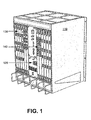
- Fig. 1 illustrates an example device 100 in which systems and methods consistent with the principles of the invention may be implemented.
- device 100 may include a housing 110 that houses various modules 120 (e.g., controller, power supply, etc.) and card slots 130 which operably receive interface cards 140.
- modules 120 e.g., controller, power supply, etc.
- card slots 130 which operably receive interface cards 140.
- device 100 may include any device that receives, processes, and/or transmits data, such as a server, a router, or a switch.
- housing 110 may include any structure configurable to retain and/or support a chassis, removable cards, and/or other modules that may be used in operation of device 100.
- the number and type of cards, modules, and other system components illustrated in Fig. 1 are provided for simplicity. In practice, a typical device could include more or fewer cards, modules, and other removable or fixed components that aid in receiving, processing, and/or transmitting data, than what is illustrated in Fig. 1.
- Housing 110 may be fabricated from metal, plastic, and/or composite and may be sized for particular applications. In one implementation, housing 110 may be sized to fit an industry standard mounting structure, such as an equipment rack.
- Fig. 2 illustrates an example interface card 140 in an orientation representative of being configured in card slot 130 in housing 110 (Fig. 1), for which airflow may be represented by the directional arrows shown. It should be appreciated that the cooling effect produced by the airflow may not be uniform over the various surfaces of interface card 140.
- Fig. 3 illustrates an internal view of one end of an example interface card 340.
- Interface card 340 may include a motherboard 350 and an interface unit 360.
- Motherboard 350 may include any substrate, such as a circuit board, e.g., a printed circuit board (PCB).
- Interface card 340 may include more than one interface unit 360.
- Interface unit 360 may include a daughterboard 362, interface module cages 364 for receiving interface modules 366, and heat sinks 368. In one implementation, interface modules 366 may attach directly to daughterboard 362 and interface module cages 364 are omitted. Interface unit 360 may include any input/output device, such as a small form-factor pluggable (SFP) interface, an XFP (10 Gigabit SFP), or any type of transceiver. Interface unit 360 may electrically, structurally, and/or thermally connect to motherboard 350. Interface unit 360 may be located at a user-accessible end of motherboard 350. Other configurations are possible.
- SFP small form-factor pluggable
- XFP 10 Gigabit SFP
- Daughterboard 362 may include any substrate, such as a PCB.
- Daughterboard 362 may have any dimensions corresponding to the dimensions of interface card 340.
- motherboard 350 may include interface unit 360. That is, motherboard 350 and interface unit 360 may be an integral PCB, without a separate daughterboard 362.
- Interface module cages 364 may include any device for receiving and retaining interface modules 366. Interface module cages 364 may include ganged individual module cages. Other configurations of interface module cages 364 are possible. As shown, interface module cages 364 may be arranged on opposing sides of daughterboard 362. Interface modules 366 may include any electronic component and/or circuitry, such as an SFP module, e.g., an SFP optical modular transceiver. In one implementation, interface modules 366 are hot-swappable.
- Heat sinks 368 may include any device that may absorb, conduct, radiate, and/or dissipate heat. Heat sinks 368 may include any material having any thermal conductivity. Heat sinks 368 may have any shape or dimensions. Any number of heat sinks 368 may be used. Thermal conductivity properties of any one heat sink 368 may vary from another heat sink 368. As shown, heat sinks 368 may be disposed at a remote end of daughterboard 362. Other configurations of the heat sinks 368 are possible. For example, heat sinks 368 may be disposed on two or more surfaces on daughterboard 362. In one implementation, the location of heat sinks 368 is based on an airflow in device 100.
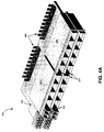
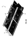
- Figs. 4A and 4B illustrate opposing views of an example interface unit 360.
- interface unit 360 may include four interface module cages 364, two side-by-side mounted at a mounting area of a first surface of daughterboard 362, and two side-by-side mounted at a mounting area of an opposite second surface of daughterboard 362 along an accessible edge of interface unit 360.
- Other configurations may be used. Any mechanism may be used to mount interface module cages 364 to daughterboard 362.
- a thermal interface material (not shown) is interposed between a mounting surface of interface module cages 364 and the mounting area on the surface of daughterboard 362.
- two interface modules 366 are respectively plugged into two interface module cages 364.
- Interface unit 360 may include heat sinks 368 attached to daughterboard 362 at an attachment area by attachment members 470 (Fig. 4B). Other attachment mechanisms may be used.
- a thermal interface material (not shown) is interposed between a mounting surface of heat sinks 368 and the attachment area on the surface of daughterboard 362.
- Fig. 4C illustrates an exploded view of interface unit 360.
- Daughterboard 362 may include thermal vias 480A that terminate on a surface of daughterboard 362 in an area of interface module cages 364 and terminate on an opposing surface of daughterboard 362.
- Daughterboard 362 may include thermal vias 480B that terminate on a surface of daughterboard 362 in an area of heat sinks 368 and extend to an interior of daughterboard 362.
- Daughterboard 362 may include thermal planes 490.
- Thermal planes 490 may be exposed at the edge of daughterboard 362.
- Thermal planes 490 may alternatively not be exposed at the edge of daughterboard 362.
- Thermal planes 490 may be electrically insulated from electrical connections, electrical vias, or electrical planes. Thermal planes may alternately include power planes, ground planes, and the like.
- Fig. 5 illustrates a partial line image of daughterboard 362, showing an internal construction thereof.
- Thermal vias 480A and 480B may include one or more through-holes that extend from a surface of daughterboard 362 to an interior of daughterboard 362.
- thermal vias 480A and 480B may extend from one surface of daughterboard 362 to an opposing surface of daughterboard 362.
- Thermal planes 490 may include one or more thermal conducting layers separated by substrate layers of daughterboard 362. Thermal planes 490 may be configured substantially parallel to daughterboard 362. Thermal planes 490 may extend from thermal vias 480A to thermal vias 480B. Thermal planes 490 may be exposed at an edge of daughterboard 362. Any of thermal vias 480A may thermally couple to any or each of thermal planes 490, and any of thermal planes 490 may thermally couple to any or each of thermal vias 480B.
- Thermal vias 480A and 480B may form a uniform pattern on the surface of daughterboard 362. Thermal vias 480A and 480B may alternatively be non-uniformly arranged on the surface of daughterboard 362. Thermal vias 480A and 480B may extend substantially perpendicularly from the surface to an interior of daughterboard 362. Thermal vias 480A and 480B may alternatively extend at any angle from the surface to an interior of daughterboard 362. Thermal vias 480A and 480B may have a substantially circular cross-section. Thermal vias 480A and 480B may alternatively have cross-sections of any other regular or irregular shape. Thermal vias 480A and 480B may have any diameter that is substantially constant from end to end. Thermal vias 480A and 480B may alternatively have diameters that vary over a length thereof. Any of thermal vias 480A and 480B may vary one from another in any of the above respects.
- a periphery of thermal vias 480A may correspond to a perimeter of interface module cages 364, i.e., define a mounting area for interface module cages 364 on a surface of daughterboard 362.
- the total effective surface area of thermal vias 480A at the surface of daughterboard 362 may constitute any portion of the total area of the mounting area of interface module cages 364.
- Some of thermal vias 480A may alternatively not be covered by interface module cages 364.
- the mounting surfaces of interface module cages 364 may overlap the periphery of thermal vias 480A.
- a periphery of thermal vias 480B may correspond to a perimeter of heat sinks 368, i.e., define a mounting area for heat sinks 368 on a surface of daughterboard 362.
- the total effective surface area of thermal vias 480B at the surface of daughterboard 362 may constitute any portion of the total area of the mounting area of heat sinks 368.
- Some of thermal vias 480B may alternatively not be covered by heat sinks 368.
- the mounting surfaces of heat sinks 368 may overlap the periphery of thermal vias 480A.
- Thermal vias 480A and 480B may include blind vias that extend from a surface of daughterboard 362 to a predetermined depth of daughterboard 362.
- Thermal vias 480A and 480B may include backdrilled vias that extend from a predetermined depth of an interior of daughterboard 362 to another predetermined depth of an interior of daughterboard 362.
- backdrilled vias may interconnect one or more thermal layers 490.
- Thermal vias 480A and 480B may include plated through-holes.
- the plating may be disposed on all or any portion of the circumference of the through-holes.
- the plating may be any one or more materials having any thermal conductivity.
- the plating may occupy any portion of the volume of the through-holes.
- the plating may form a hollow cylinder having an outer diameter and an inner diameter.
- the inner diameter of the plating may be filled or partially filled with a second material, for example, a soldering material.
- Any of thermal vias 480A and 480B may vary one from another in any of the above respects.
- Thermal planes 490 may include any of one or more materials having any thermal conductivity.
- thermal planes 490 may include a thermal conductive layer on all or any portion of a surface of daughterboard 362.
- Thermal planes 490 may have a substantially constant cross-section.
- Thermal planes 490 may alternatively have a varying cross-section along a length thereof. Any of thermal planes 490 may vary one from another in any of these respects.
- an inner-most thermal plane 490 may have the largest effective cross-sectional area relative to other thermal planes 490.
- a thermal plane 490 that is the greatest distance from interface module cages 364 may have the largest effective cross-sectional area relative to other thermal planes 490.
- Daughterboard 362 may be formed according to any standard technique for forming a PCB.
- a layer of copper may be affixed to a layer of an insulating substrate. Patterns may be etched in the copper layer. Additional copper/insulating layers may be laminated to the substrate with etched patterns.
- a four-ounce copper is used for the copper layers. Other thicknesses of copper may be used. The thickness of the copper may be thicker by any factor than a copper layer thickness (e.g., 1 ⁇ 2 oz.) used for electrical connections.
- Through-holes may be drilled, backdrilled, or otherwise formed in the copper/insulator layers. The through-holes may be plated by electrolytic plating or any other suitable technique. In one implementation, a soldering material is then flowed in the plated through-holes.
- thermal vias 480A and 480B and/or thermal planes 490 may be based on factors such as structural integrity, electrical connectivity, and optimal thermal conductivity.
- thermal vias 480A and 480B and thermal planes 490 may be electrically insulated from electrical connections (not shown) in daughterboard 362.
- thermal vias 480A and 480B and/or thermal planes 490 may be formed based on heat generation and/or thermal sensitivity of particular interface modules 366, as described in more detail below.
- Fig. 6 is a flowchart of example thermal management 600 in a device, such as device 100, according to an implementation consistent with principles of the invention.
- Thermal management 600 may begin with generation of heat from interface module 366, such as an active transceiver, during operations performed by device 100 (act 610). At least a portion of the generated heat may be conducted to an interface module cage 364, in which interface module 366 is plugged (act 620). At least a portion of the heat absorbed by interface module cage 364 may be conducted to thermal vias 480A having a terminal end in an area directly under or near a mounting surface of interface module cage 364 (act 630). In one implementation, one or more thermal vias 480A may directly contact interface module cage 364.
- At least a portion of the heat conducted to the one or more thermal vias 480A may be conducted to one or more thermal planes 490 (act 640). At least a portion of the heat conducted by the one or more thermal planes 490 may be conducted to thermal vias 480B (act 650). At least a portion of the heat conducted to thermal vias 480B may be conducted to heat sink 368, an attachment portion thereof which may be directly over or near a terminal end of thermal vias 480B (act 660). At least a portion of the heat absorbed by heat sink 368 may be dissipated into available airflow in device 100 (act 670).
- thermal management 600 may instead be initiated by interface module 366, such as an inactive transceiver, which acts as a secondary heat source, having absorbed heat from a primary source that has generated the heat (e.g., an active transceiver or other component).
- interface module 366 such as an inactive transceiver, which acts as a secondary heat source, having absorbed heat from a primary source that has generated the heat (e.g., an active transceiver or other component).
- the heat path described above may be specific to an associated individual interface module cage 364 in interface unit 360. That is, the effective heat conductivity of an associated heat path may be managed for any given interface module cage 364. The effective heat conductivity of an associated heat path may be based on such factors as the location of the individual interface module cage 364 in interface unit 360, the performance level (i.e., heat generation) of interface module 366 associated with the individual interface module cage 364, the heat sensitivity of interface module 366 associated with the individual interface module cage 364, and thermal gradients experienced over interface unit 360, generally. In this manner, the heat transfer rate (i.e., cooling effect) may be managed from one interface module 366 to another.
- the heat transfer rate i.e., cooling effect
- Optimizing thermal transfer among interface modules 366, or varying the effective thermal conductivity associated with particular heat paths, may be achieved through the geometries of and interconnection formed by thermal vias 480A and 480B and thermal planes 490.
- thermal vias 480A may have effective thermal conductivities that differ one from another;
- thermal planes 490 may have effective thermal conductivities that differ one from another; and
- thermal vias 480B may have effective thermal conductivities that differ one from another.
- Sets of thermal vias 480A associated with particular areas of daughterboard 362 may differ one from another.
- Implementations consistent with the principles of the invention make possible efficient heat management in a device employing PCBs having clustered components, including an interface device, a memory, a processor, and other types of devices.
- heat transfer may be optimized for any given input/output module through interconnected vias and thermal planes in a substrate of an interface unit of an interface card, thereby controlling the temperature of the input/output module.
Landscapes
- Physics & Mathematics (AREA)
- Engineering & Computer Science (AREA)
- Microelectronics & Electronic Packaging (AREA)
- Thermal Sciences (AREA)
- General Physics & Mathematics (AREA)
- Optics & Photonics (AREA)
- Aviation & Aerospace Engineering (AREA)
- Cooling Or The Like Of Electrical Apparatus (AREA)
- Cooling Or The Like Of Semiconductors Or Solid State Devices (AREA)
Abstract
Description
- Implementations consistent with the principles of the invention relate generally to heat dissipation and, more particularly, to systems and methods of heat transfer through a substrate supporting electronic components to control operating temperatures of the electronic components.
- Physical compactness of electronic devices, such as interface devices mounted at a user interface edge of an electronic assembly, impedes cooling of the electronic devices, which is a particular concern for electronic devices that consume a substantial amount of power, and thus generate a significant amount of heat. For example, when transceivers, such as small form-factor pluggable (SFP) modules, are ganged into multiple cages, the transceivers in the middle of the cluster may generate and retain an undesirable amount of heat. Very little airflow may reach individual modules in certain positions of the cluster for cooling purposes. Unlike stand-alone devices, which have relatively large surface areas that may radiate heat, clustered devices may have only limited surface area from which to radiate heat.
- According to one aspect, a device may include a substrate that may include a first mounting area on a first surface of the substrate. The device may also include a group of first thermal vias extending from the first mounting area to at least an interior of the substrate. The device may also include at least one thermal plane substantially parallel to the first surface of the substrate, the at least one thermal plane being in thermal contact with at least one of the first thermal vias. The device may also include a heat sink attachment area. In addition, the device may include a group of second thermal vias extending from the heat sink attachment area to the interior of the substrate, the at least one thermal plane being in thermal contact with the second thermal vias.
- According to another aspect, a method of heat transfer in a substrate may include conducting heat from a component to a component mount mounted on a first mounting surface of the substrate. The method may also include conducting the heat from the component mount to a first set of thermal vias that extend from the first mounting surface to at least an interior of the substrate. The method may also include conducting the heat from the first set of thermal vias to one or more thermal planes disposed along a length of the substrate. The method may also include conducting the heat from the one or more thermal planes to a second set of thermal vias. The method may also include conducting the heat from the second set of thermal vias to a heat sink attachment surface of the substrate. In addition, the method may include conducting the heat from the heat sink attachment surface of the substrate to a heat sink mounted to a heat sink attachment surface of the substrate.
- According to yet another aspect, a method of forming a substrate may include disposing one or more thermal planes in the substrate. The method may also include providing a first set of thermal vias in a component mounting area on a first side of the substrate, the first set of the thermal vias being thermally coupled to the component mounting area and to the one or more thermal planes. In addition, the method may include providing a second set of thermal vias extending from a heat sink attachment area on the first side of the substrate, the second set of the thermal vias being thermally coupled to the one or more planes and to the heat sink attachment area.
- The accompanying drawings, which are incorporated in and constitute a part of this specification, illustrate an example implementation of the invention and, together with the description, explain the invention. In the drawings,
- Fig. 1 is a diagram illustrating an example device in which methods and systems consistent with the principles of the invention can be implemented;
- Fig. 2 is an example diagram of the interface card of Fig. 1 according to an implementation consistent with the principles of the invention;
- Fig. 3 is a cut-away view of an example interface card in which methods and systems consistent with the principles of the invention can be implemented;
- Figs. 4A, 4B, and 4C illustrate an example interface unit in which methods and systems consistent with the principles of the invention can be implemented;
- Fig. 5 is a line image of the example daughterboard of Figs. 4A-4C; and
- Fig. 6 is a flow diagram of an example thermal management process according to an implementation consistent with the principles of the invention.
- The following detailed description of embodiments of the principles of the invention refers to the accompanying drawings. The same reference numbers in different drawings may identify the same or similar elements. Also, the following detailed description does not limit the invention. Instead, the scope of the invention is defined by the appended claims and equivalents.
- Systems and methods consistent with the principles of the invention may provide controlled cooling of a component, such as an input/output device, that may be located in a compact configuration at a user interface edge of an interface card, by conducting heat away from the component using a system of thermally coupled thermal vias and thermal planes on and/or in a substrate to a heat sink that may be disposed in an available airflow that may flow by the interface card.
- Fig. 1 illustrates an example device 100 in which systems and methods consistent with the principles of the invention may be implemented. As illustrated, device 100 may include a
housing 110 that houses various modules 120 (e.g., controller, power supply, etc.) andcard slots 130 which operably receiveinterface cards 140. - In one implementation, device 100 may include any device that receives, processes, and/or transmits data, such as a server, a router, or a switch.
- In one implementation,
housing 110 may include any structure configurable to retain and/or support a chassis, removable cards, and/or other modules that may be used in operation of device 100. The number and type of cards, modules, and other system components illustrated in Fig. 1 are provided for simplicity. In practice, a typical device could include more or fewer cards, modules, and other removable or fixed components that aid in receiving, processing, and/or transmitting data, than what is illustrated in Fig. 1.Housing 110 may be fabricated from metal, plastic, and/or composite and may be sized for particular applications. In one implementation,housing 110 may be sized to fit an industry standard mounting structure, such as an equipment rack. - Fig. 2 illustrates an
example interface card 140 in an orientation representative of being configured incard slot 130 in housing 110 (Fig. 1), for which airflow may be represented by the directional arrows shown. It should be appreciated that the cooling effect produced by the airflow may not be uniform over the various surfaces ofinterface card 140. - Fig. 3 illustrates an internal view of one end of an
example interface card 340.Interface card 340 may include amotherboard 350 and aninterface unit 360. Motherboard 350 may include any substrate, such as a circuit board, e.g., a printed circuit board (PCB).Interface card 340 may include more than oneinterface unit 360. -
Interface unit 360 may include adaughterboard 362,interface module cages 364 for receivinginterface modules 366, andheat sinks 368. In one implementation,interface modules 366 may attach directly todaughterboard 362 andinterface module cages 364 are omitted.Interface unit 360 may include any input/output device, such as a small form-factor pluggable (SFP) interface, an XFP (10 Gigabit SFP), or any type of transceiver.Interface unit 360 may electrically, structurally, and/or thermally connect tomotherboard 350.Interface unit 360 may be located at a user-accessible end ofmotherboard 350. Other configurations are possible. - Daughterboard 362 may include any substrate, such as a PCB. Daughterboard 362 may have any dimensions corresponding to the dimensions of
interface card 340. In one implementation,motherboard 350 may includeinterface unit 360. That is,motherboard 350 andinterface unit 360 may be an integral PCB, without aseparate daughterboard 362. -
Interface module cages 364 may include any device for receiving and retaininginterface modules 366.Interface module cages 364 may include ganged individual module cages. Other configurations ofinterface module cages 364 are possible. As shown,interface module cages 364 may be arranged on opposing sides ofdaughterboard 362.Interface modules 366 may include any electronic component and/or circuitry, such as an SFP module, e.g., an SFP optical modular transceiver. In one implementation,interface modules 366 are hot-swappable. - Heat sinks 368 may include any device that may absorb, conduct, radiate, and/or dissipate heat. Heat sinks 368 may include any material having any thermal conductivity. Heat sinks 368 may have any shape or dimensions. Any number of
heat sinks 368 may be used. Thermal conductivity properties of any oneheat sink 368 may vary from anotherheat sink 368. As shown,heat sinks 368 may be disposed at a remote end ofdaughterboard 362. Other configurations of theheat sinks 368 are possible. For example,heat sinks 368 may be disposed on two or more surfaces ondaughterboard 362. In one implementation, the location ofheat sinks 368 is based on an airflow in device 100. - Figs. 4A and 4B illustrate opposing views of an
example interface unit 360. As shown,interface unit 360 may include fourinterface module cages 364, two side-by-side mounted at a mounting area of a first surface ofdaughterboard 362, and two side-by-side mounted at a mounting area of an opposite second surface ofdaughterboard 362 along an accessible edge ofinterface unit 360. Other configurations may be used. Any mechanism may be used to mountinterface module cages 364 todaughterboard 362. In one implementation, a thermal interface material (not shown) is interposed between a mounting surface ofinterface module cages 364 and the mounting area on the surface ofdaughterboard 362. As shown, twointerface modules 366 are respectively plugged into twointerface module cages 364.Interface unit 360 may includeheat sinks 368 attached todaughterboard 362 at an attachment area by attachment members 470 (Fig. 4B). Other attachment mechanisms may be used. In one implementation, a thermal interface material (not shown) is interposed between a mounting surface ofheat sinks 368 and the attachment area on the surface ofdaughterboard 362. - Fig. 4C illustrates an exploded view of
interface unit 360.Daughterboard 362 may includethermal vias 480A that terminate on a surface ofdaughterboard 362 in an area ofinterface module cages 364 and terminate on an opposing surface ofdaughterboard 362.Daughterboard 362 may includethermal vias 480B that terminate on a surface ofdaughterboard 362 in an area ofheat sinks 368 and extend to an interior ofdaughterboard 362.Daughterboard 362 may includethermal planes 490.Thermal planes 490 may be exposed at the edge ofdaughterboard 362.Thermal planes 490 may alternatively not be exposed at the edge ofdaughterboard 362.Thermal planes 490 may be electrically insulated from electrical connections, electrical vias, or electrical planes. Thermal planes may alternately include power planes, ground planes, and the like. - Fig. 5 illustrates a partial line image of
daughterboard 362, showing an internal construction thereof.Thermal vias daughterboard 362 to an interior ofdaughterboard 362. In one implementation,thermal vias daughterboard 362 to an opposing surface ofdaughterboard 362.Thermal planes 490 may include one or more thermal conducting layers separated by substrate layers ofdaughterboard 362.Thermal planes 490 may be configured substantially parallel todaughterboard 362.Thermal planes 490 may extend fromthermal vias 480A tothermal vias 480B.Thermal planes 490 may be exposed at an edge ofdaughterboard 362. Any ofthermal vias 480A may thermally couple to any or each ofthermal planes 490, and any ofthermal planes 490 may thermally couple to any or each ofthermal vias 480B. -
Thermal vias daughterboard 362.Thermal vias daughterboard 362.Thermal vias daughterboard 362.Thermal vias daughterboard 362.Thermal vias Thermal vias Thermal vias Thermal vias thermal vias - A periphery of
thermal vias 480A may correspond to a perimeter ofinterface module cages 364, i.e., define a mounting area forinterface module cages 364 on a surface ofdaughterboard 362. The total effective surface area ofthermal vias 480A at the surface ofdaughterboard 362 may constitute any portion of the total area of the mounting area ofinterface module cages 364. Some ofthermal vias 480A may alternatively not be covered byinterface module cages 364. Alternatively, the mounting surfaces ofinterface module cages 364 may overlap the periphery ofthermal vias 480A. - A periphery of
thermal vias 480B may correspond to a perimeter ofheat sinks 368, i.e., define a mounting area forheat sinks 368 on a surface ofdaughterboard 362. The total effective surface area ofthermal vias 480B at the surface ofdaughterboard 362 may constitute any portion of the total area of the mounting area of heat sinks 368. Some ofthermal vias 480B may alternatively not be covered byheat sinks 368. Alternatively, the mounting surfaces ofheat sinks 368 may overlap the periphery ofthermal vias 480A. -
Thermal vias daughterboard 362 to a predetermined depth ofdaughterboard 362.Thermal vias daughterboard 362 to another predetermined depth of an interior ofdaughterboard 362. In one implementation, backdrilled vias may interconnect one or morethermal layers 490. -
Thermal vias thermal vias -
Thermal planes 490 may include any of one or more materials having any thermal conductivity. In one implementation,thermal planes 490 may include a thermal conductive layer on all or any portion of a surface ofdaughterboard 362.Thermal planes 490 may have a substantially constant cross-section.Thermal planes 490 may alternatively have a varying cross-section along a length thereof. Any ofthermal planes 490 may vary one from another in any of these respects. In one implementation, for example, an inner-mostthermal plane 490 may have the largest effective cross-sectional area relative to otherthermal planes 490. In another implementation, athermal plane 490 that is the greatest distance frominterface module cages 364 may have the largest effective cross-sectional area relative to otherthermal planes 490. -
Daughterboard 362 may be formed according to any standard technique for forming a PCB. For example, a layer of copper may be affixed to a layer of an insulating substrate. Patterns may be etched in the copper layer. Additional copper/insulating layers may be laminated to the substrate with etched patterns. In one implementation, a four-ounce copper is used for the copper layers. Other thicknesses of copper may be used. The thickness of the copper may be thicker by any factor than a copper layer thickness (e.g., ½ oz.) used for electrical connections. Through-holes may be drilled, backdrilled, or otherwise formed in the copper/insulator layers. The through-holes may be plated by electrolytic plating or any other suitable technique. In one implementation, a soldering material is then flowed in the plated through-holes. - The dimensions and geometries of
thermal vias thermal planes 490 may be based on factors such as structural integrity, electrical connectivity, and optimal thermal conductivity. For example,thermal vias thermal planes 490 may be electrically insulated from electrical connections (not shown) indaughterboard 362. As another example,thermal vias thermal planes 490 may be formed based on heat generation and/or thermal sensitivity ofparticular interface modules 366, as described in more detail below. - Fig. 6 is a flowchart of example
thermal management 600 in a device, such as device 100, according to an implementation consistent with principles of the invention.Thermal management 600 may begin with generation of heat frominterface module 366, such as an active transceiver, during operations performed by device 100 (act 610). At least a portion of the generated heat may be conducted to aninterface module cage 364, in whichinterface module 366 is plugged (act 620). At least a portion of the heat absorbed byinterface module cage 364 may be conducted tothermal vias 480A having a terminal end in an area directly under or near a mounting surface of interface module cage 364 (act 630). In one implementation, one or morethermal vias 480A may directly contactinterface module cage 364. At least a portion of the heat conducted to the one or morethermal vias 480A may be conducted to one or more thermal planes 490 (act 640). At least a portion of the heat conducted by the one or morethermal planes 490 may be conducted tothermal vias 480B (act 650). At least a portion of the heat conducted tothermal vias 480B may be conducted toheat sink 368, an attachment portion thereof which may be directly over or near a terminal end ofthermal vias 480B (act 660). At least a portion of the heat absorbed byheat sink 368 may be dissipated into available airflow in device 100 (act 670). - It will be appreciated that
thermal management 600 may instead be initiated byinterface module 366, such as an inactive transceiver, which acts as a secondary heat source, having absorbed heat from a primary source that has generated the heat (e.g., an active transceiver or other component). - In one implementation, the heat path described above may be specific to an associated individual
interface module cage 364 ininterface unit 360. That is, the effective heat conductivity of an associated heat path may be managed for any giveninterface module cage 364. The effective heat conductivity of an associated heat path may be based on such factors as the location of the individualinterface module cage 364 ininterface unit 360, the performance level (i.e., heat generation) ofinterface module 366 associated with the individualinterface module cage 364, the heat sensitivity ofinterface module 366 associated with the individualinterface module cage 364, and thermal gradients experienced overinterface unit 360, generally. In this manner, the heat transfer rate (i.e., cooling effect) may be managed from oneinterface module 366 to another. - Optimizing thermal transfer among
interface modules 366, or varying the effective thermal conductivity associated with particular heat paths, may be achieved through the geometries of and interconnection formed bythermal vias thermal planes 490. For example,thermal vias 480A may have effective thermal conductivities that differ one from another;thermal planes 490 may have effective thermal conductivities that differ one from another; and/orthermal vias 480B may have effective thermal conductivities that differ one from another. Sets ofthermal vias 480A associated with particular areas ofdaughterboard 362 may differ one from another. - Implementations consistent with the principles of the invention make possible efficient heat management in a device employing PCBs having clustered components, including an interface device, a memory, a processor, and other types of devices. For example, heat transfer may be optimized for any given input/output module through interconnected vias and thermal planes in a substrate of an interface unit of an interface card, thereby controlling the temperature of the input/output module.
- The foregoing description of example embodiments of the invention provides illustration and description, but is not intended to be exhaustive or to limit the invention to the precise form disclosed. Modifications and variations are possible in light of the above teachings or may be acquired from practice of the invention.
- For example, implementations consistent with the principles of the invention can be implemented using assemblies and parts other than those illustrated in the figures and described in the specification without departing from the spirit of the invention. Parts may be added and/or removed from device 100,
interface unit 360, and/ordaughterboard 362 depending on specific deployments and/or applications. Further, disclosed implementations may not be limited to any specific combination of components. - No element, act, or instruction used in the description of the invention should be construed as critical or essential to the invention unless explicitly described as such. Also, as used herein, the article "a" is intended to include one or more items. Where only one item is intended, the term "one" or similar language is used. Further, the phrase "based on," as used herein is intended to mean "based, at least in part, on" unless explicitly stated otherwise.
Claims (27)
- A device comprising:a substrate including:a first mounting area on a first surface of the substrate;a plurality of first thermal vias extending from the first mounting area to at least an interior of the substrate;at least one thermal plane substantially parallel to the first surface of the substrate, the at least one thermal plane being in thermal contact with at least one of the first thermal vias;a heat sink attachment area; anda plurality of second thermal vias extending from the heat sink attachment area to the interior of the substrate, the at least one thermal plane being in thermal contact with the second thermal vias.
- The device of claim 1, the substrate further comprising:a second mounting area located on a second surface of the substrate opposing the first surface of the substrate, at least one the first thermal vias extending from the first mounting area to the second mounting area.
- The device of claim 1 or claim 2, wherein the at least one thermal plane comprises at least a portion of the first mounting area and at least a portion of the heat sink attachment area.
- The device of claim 3, wherein at least one of the first thermal vias has a thermal conductivity that differs from a thermal conductivity of another one of the first thermal vias.
- The device of any preceding claim, wherein the at least one thermal plane comprises two or more thermal planes, a first of the two or more thermal planes having a first cross-sectional area and a second of the two or more thermal planes having a second cross-sectional area.
- The device of claim 5, the first cross-sectional area being based on a distance of the first of the two or more thermal planes from the first mounting area, and the second cross-sectional area being based on a distance of the second of the two or more thermal planes from the first mounting area.
- The device of any preceding claim, wherein the first thermal vias comprise a non-uniform configuration in the first mounting area.
- The device of any preceding claim, wherein a number of the first thermal vias per unit area of the first mounting area is based on a predetermined location on the first surface of the substrate.
- The device of any preceding claim, further comprising:a component mount mounted to the substrate at the first mounting surface area, wherein at least one of the first thermal vias thermally contacts the component mount.
- The device of any preceding claim, further comprising:a heat sink mounted to the substrate at the heat sink attachment area; anda thermal interface material interposed between a mounting surface of the heat sink and the heat sink attachment area, wherein the thermal interface material is in thermal contact with the second thermal vias.
- The device of any preceding claim, wherein the at least one thermal plane comprises two or more thermal planes, one or more layers of the substrate being interposed between the two or more thermal planes.
- The device of claim 11, wherein a first of the two or more thermal planes and a second of the two or more thermal planes are in thermal contact with a same group of the first thermal vias.
- The device of claim 11, wherein a first of the two or more thermal planes thermally contacts at least some of the first thermal vias that do not thermally contact a second of the two or more thermal planes.
- A method of heat transfer in a substrate, comprising:conducting heat from a component to a component mount mounted on a first mounting surface of the substrate;conducting the heat from the component mount to a first set of thermal vias that extend from the first mounting surface to at least an interior of the substrate;conducting the heat from the first set of thermal vias to one or more thermal planes disposed along a length of the substrate;conducting the heat from the one or more thermal planes to a second set of thermal vias; andconducting the heat from the second set of thermal vias to a heat sink mounted to a heat sink attachment surface of the substrate.
- The method of claim 14, further comprising:conducting the heat from the second set of thermal vias to a heat transfer material interposed between the second set of thermal vias and a mount portion of the heat sink.
- The method of claim 14 or claim 15, wherein the conducting the heat from the first set of thermal vias to the one or more thermal planes comprises conducting the heat via through-holes including a first material having a first thermal conductivity and a second material having a second thermal conductivity.
- The method of any of claims 14 to 16, wherein the first set of the thermal vias comprise a non-uniform distribution at the first mounting surface.
- The method of any of claims 14 to 17, wherein the conducting the heat from the component mount to the heat sink comprises a first thermal path, a first thermal conductivity being associated with the first thermal path, the method further comprising:conducting additional heat from a second component to the component mount;conducting the additional heat from the component mount to the heat sink via a second thermal path, a second thermal conductivity being associated with the second thermal path.
- A method of forming a substrate comprising:disposing one or more thermal planes in the substrate;providing a first set of thermal vias in a component mounting area on a first side of the substrate, the first set of the thermal vias being thermally coupled to the component mounting area and to the one or more thermal planes; andproviding a second set of thermal vias extending from a heat sink attachment area on the first side of the substrate, the second set of the thermal vias being thermally coupled to the one or more planes and to the heat sink attachment area.
- The method of claim 19, wherein the disposing one or more thermal planes comprises embedding one or more thermal planes in the substrate, the one or more thermal planes having varying cross-sectional areas based on a distance of the embedded planes from the mounting area.
- The method of claim 19 or claim 20, wherein the providing the first set of thermal vias comprises providing through-holes extending from the component mounting area to an interior of the substrate, the through-holes having varying diameters.
- The method of any of claims 19 to 21, further comprising:providing a thermal interface material on at least a portion of the heat sink attachment area, the second set of the thermal vias being thermally coupled to the thermal interface material.
- The method of any of claims 19 to 22, wherein the providing the first set of the thermal vias comprises providing a plurality of through-holes that extend from the component mounting area to a second component mounting area on an opposing side of the substrate, the plurality of through-holes being thermally coupled to the first and second component mounting areas.
- The method of any of claims 19 to 23, wherein the providing the first set of the thermal vias comprises providing a plurality of through-holes and plating at least a portion of a circumference of the plurality of through-holes with a thermal conductor.
- The method of claim 24, wherein the plating comprises plating a first of the plurality of through-holes with a first thermal conductor having a first thermal conductivity, and plating a second of the plurality of through-holes with a second thermal conductor having a second thermal conductivity.
- The method of claim 24 or claim 25, wherein the plating comprises plating a first of the plurality of through-holes with a first volume of the thermal conductor, and plating a second of the plurality of through-holes with a second volume of thermal conductor.
- The method of any of claims 24 to 26, wherein the providing the plurality of through-holes further comprises at least partially filling the volume of the plated through-hole with a second thermal conductor.
Applications Claiming Priority (1)
| Application Number | Priority Date | Filing Date | Title |
|---|---|---|---|
| US11/363,095 US7629683B1 (en) | 2006-02-28 | 2006-02-28 | Thermal management of electronic devices |
Publications (3)
| Publication Number | Publication Date |
|---|---|
| EP1827070A2 true EP1827070A2 (en) | 2007-08-29 |
| EP1827070A3 EP1827070A3 (en) | 2009-05-13 |
| EP1827070B1 EP1827070B1 (en) | 2017-10-18 |
Family
ID=38144264
Family Applications (1)
| Application Number | Title | Priority Date | Filing Date |
|---|---|---|---|
| EP07250789.0A Active EP1827070B1 (en) | 2006-02-28 | 2007-02-26 | Thermal management of electronic devices |
Country Status (3)
| Country | Link |
|---|---|
| US (3) | US7629683B1 (en) |
| EP (1) | EP1827070B1 (en) |
| CN (2) | CN101052268B (en) |
Cited By (2)
| Publication number | Priority date | Publication date | Assignee | Title |
|---|---|---|---|---|
| CN114190011A (en) * | 2021-11-11 | 2022-03-15 | 江苏普诺威电子股份有限公司 | High-heat-dissipation PCB and manufacturing process thereof |
| DE102012205893B4 (en) | 2011-04-11 | 2022-08-25 | Broadcom International Pte. Ltd. | Balanced cooling system and method for high density stacked cages |
Families Citing this family (26)
| Publication number | Priority date | Publication date | Assignee | Title |
|---|---|---|---|---|
| US7629683B1 (en) * | 2006-02-28 | 2009-12-08 | Juniper Networks, Inc. | Thermal management of electronic devices |
| US7826222B2 (en) * | 2008-07-03 | 2010-11-02 | Juniper Networks, Inc. | Front-to-back cooling system for modular systems with orthogonal midplane configuration |
| US7804684B1 (en) | 2008-12-22 | 2010-09-28 | Juniper Networks, Inc. | Cooling system for a data processing unit |
| US7787249B2 (en) * | 2009-02-03 | 2010-08-31 | Honeywell International Inc. | Systems and methods for printed board assembly isolated heat exchange |
| US8535787B1 (en) | 2009-06-29 | 2013-09-17 | Juniper Networks, Inc. | Heat sinks having a thermal interface for cooling electronic devices |
| US8534930B1 (en) | 2009-09-24 | 2013-09-17 | Juniper Networks, Inc. | Circuit boards defining openings for cooling electronic devices |
| US8801374B1 (en) | 2009-10-07 | 2014-08-12 | Juniper Networks, Inc. | Fan trays having stator blades for improving air flow performance |
| US8223498B2 (en) * | 2009-11-11 | 2012-07-17 | Juniper Networks, Inc. | Thermal interface members for removable electronic devices |
| US8279601B2 (en) * | 2010-01-28 | 2012-10-02 | Juniper Networks, Inc. | Air flow ducts for cooling electronic devices within a data processing unit |
| US8358504B2 (en) * | 2011-01-18 | 2013-01-22 | Avago Technologies Enterprise IP (Singapore) Pte. Ltd. | Direct cooling system and method for transceivers |
| US9414437B2 (en) * | 2011-03-28 | 2016-08-09 | Telefonaktiebolaget L M Ericsson (Publ) | Radio device and method for manufacturing the radio device |
| US8824797B2 (en) | 2011-10-03 | 2014-09-02 | Xerox Corporation | Graph-based segmentation integrating visible and NIR information |
| US9900101B2 (en) * | 2012-04-30 | 2018-02-20 | Hewlett Packard Enterprise Development Lp | Transceiver module |
| US9253927B1 (en) | 2012-09-28 | 2016-02-02 | Juniper Networks, Inc. | Removable fan tray |
| US8922992B2 (en) | 2012-11-12 | 2014-12-30 | Dell Products L.P. | System and design of cost effective chassis design for networking products |
| JP6398708B2 (en) * | 2014-12-26 | 2018-10-03 | 株式会社デンソー | Electronic device and driving device using the same |
| KR102411999B1 (en) * | 2015-04-08 | 2022-06-22 | 삼성전기주식회사 | Circuit board |
| US9537291B1 (en) * | 2015-06-08 | 2017-01-03 | Amazon Technologies, Inc. | Elevated automatic transfer switch cabinet |
| US10476298B1 (en) | 2015-09-02 | 2019-11-12 | Amazon Technologies, Inc. | Elevated automatic transfer switch cabinet |
| US10965333B2 (en) | 2016-07-26 | 2021-03-30 | Laird Technologies, Inc. | Thermal management assemblies suitable for use with transceivers and other devices |
| US10389397B2 (en) | 2016-07-26 | 2019-08-20 | Laird Technologies, Inc. | Small form-factor pluggable (SFP) transceivers |
| WO2022217387A1 (en) * | 2021-04-11 | 2022-10-20 | Telefonaktiebolaget Lm Ericsson (Publ) | Circuit board assembly and radio unit comprising the same |
| US11710723B2 (en) | 2021-08-05 | 2023-07-25 | Kambix Innovations, Llc | Thermal management of three-dimensional integrated circuits |
| US11942453B2 (en) | 2021-08-05 | 2024-03-26 | Kambix Innovations, Llc | Thermal management of three-dimensional integrated circuits |
| US12598993B2 (en) | 2022-02-21 | 2026-04-07 | KV Innovations, LLC | Three-dimensional integrated circuit |
| WO2026091005A1 (en) * | 2024-10-31 | 2026-05-07 | 汤姆逊许可公司 | Adjustable heat sink structure |
Citations (3)
| Publication number | Priority date | Publication date | Assignee | Title |
|---|---|---|---|---|
| US4535385A (en) | 1983-04-22 | 1985-08-13 | Cray Research, Inc. | Circuit module with enhanced heat transfer and distribution |
| EP0600590A1 (en) | 1992-12-03 | 1994-06-08 | International Computers Limited | Cooling electronic circuit assemblies |
| US6671176B1 (en) | 2002-06-27 | 2003-12-30 | Eastman Kodak Company | Method of cooling heat-generating electrical components |
Family Cites Families (24)
| Publication number | Priority date | Publication date | Assignee | Title |
|---|---|---|---|---|
| US4739448A (en) * | 1984-06-25 | 1988-04-19 | Magnavox Government And Industrial Electronics Company | Microwave multiport multilayered integrated circuit chip carrier |
| US5027191A (en) * | 1989-05-11 | 1991-06-25 | Westinghouse Electric Corp. | Cavity-down chip carrier with pad grid array |
| JP2960276B2 (en) * | 1992-07-30 | 1999-10-06 | 株式会社東芝 | Multilayer wiring board, semiconductor device using this substrate, and method of manufacturing multilayer wiring board |
| JPH0677281U (en) * | 1993-03-31 | 1994-10-28 | ファナック株式会社 | Multilayer printed circuit board |
| JPH07235775A (en) * | 1994-02-21 | 1995-09-05 | Mitsubishi Electric Corp | Multilayer printed wiring board |
| JPH0955459A (en) * | 1995-06-06 | 1997-02-25 | Seiko Epson Corp | Semiconductor device |
| US5792677A (en) * | 1997-01-16 | 1998-08-11 | Ford Motor Company | Embedded metal planes for thermal management |
| US6069793A (en) * | 1997-01-24 | 2000-05-30 | Hitachi, Ltd. | Circuit module and information processing apparatus |
| JP2914342B2 (en) | 1997-03-28 | 1999-06-28 | 日本電気株式会社 | Cooling structure of integrated circuit device |
| TW430959B (en) * | 1998-04-22 | 2001-04-21 | World Wiser Electronics Inc | Thermal enhanced structure of printed circuit board |
| US6377464B1 (en) * | 1999-01-29 | 2002-04-23 | Conexant Systems, Inc. | Multiple chip module with integrated RF capabilities |
| WO2002096166A1 (en) * | 2001-05-18 | 2002-11-28 | Corporation For National Research Initiatives | Radio frequency microelectromechanical systems (mems) devices on low-temperature co-fired ceramic (ltcc) substrates |
| US6683512B2 (en) * | 2001-06-21 | 2004-01-27 | Kyocera Corporation | High frequency module having a laminate board with a plurality of dielectric layers |
| US6592269B1 (en) * | 2001-08-31 | 2003-07-15 | Cypress Semiconductor Corporation | Apparatus and method for integrating an optical transceiver with a surface mount package |
| EP1394857A3 (en) * | 2002-08-28 | 2004-04-07 | Matsushita Electric Industrial Co., Ltd. | Semiconductor device |
| US6770967B2 (en) * | 2002-12-23 | 2004-08-03 | Eastman Kodak Company | Remote thermal vias for densely packed electrical assemblage |
| US20050133929A1 (en) * | 2003-12-18 | 2005-06-23 | Howard Gregory E. | Flexible package with rigid substrate segments for high density integrated circuit systems |
| US6980437B2 (en) * | 2004-03-03 | 2005-12-27 | Tyco Electronics Corporation | Pluggable electronic receptacle with heat sink assembly |
| US7239515B2 (en) * | 2004-03-08 | 2007-07-03 | Nortel Networks Limited | Thermal assembly for cooling an electronics module |
| US7190056B2 (en) * | 2004-03-31 | 2007-03-13 | Nokia Corporation | Thermally enhanced component interposer: finger and net structures |
| US7286359B2 (en) * | 2004-05-11 | 2007-10-23 | The U.S. Government As Represented By The National Security Agency | Use of thermally conductive vias to extract heat from microelectronic chips and method of manufacturing |
| US7405474B1 (en) * | 2004-10-12 | 2008-07-29 | Cypress Semiconductor Corporation | Low cost thermally enhanced semiconductor package |
| US7148554B2 (en) * | 2004-12-16 | 2006-12-12 | Delphi Technologies, Inc. | Discrete electronic component arrangement including anchoring, thermally conductive pad |
| US7629683B1 (en) | 2006-02-28 | 2009-12-08 | Juniper Networks, Inc. | Thermal management of electronic devices |
-
2006
- 2006-02-28 US US11/363,095 patent/US7629683B1/en active Active
-
2007
- 2007-02-26 EP EP07250789.0A patent/EP1827070B1/en active Active
- 2007-02-28 CN CN2007100800149A patent/CN101052268B/en active Active
- 2007-02-28 CN CNU2007200030680U patent/CN201078873Y/en not_active Expired - Lifetime
-
2009
- 2009-10-23 US US12/605,035 patent/US7951650B2/en not_active Expired - Lifetime
-
2011
- 2011-04-20 US US13/090,375 patent/US8318546B2/en not_active Expired - Lifetime
Patent Citations (3)
| Publication number | Priority date | Publication date | Assignee | Title |
|---|---|---|---|---|
| US4535385A (en) | 1983-04-22 | 1985-08-13 | Cray Research, Inc. | Circuit module with enhanced heat transfer and distribution |
| EP0600590A1 (en) | 1992-12-03 | 1994-06-08 | International Computers Limited | Cooling electronic circuit assemblies |
| US6671176B1 (en) | 2002-06-27 | 2003-12-30 | Eastman Kodak Company | Method of cooling heat-generating electrical components |
Cited By (3)
| Publication number | Priority date | Publication date | Assignee | Title |
|---|---|---|---|---|
| DE102012205893B4 (en) | 2011-04-11 | 2022-08-25 | Broadcom International Pte. Ltd. | Balanced cooling system and method for high density stacked cages |
| CN114190011A (en) * | 2021-11-11 | 2022-03-15 | 江苏普诺威电子股份有限公司 | High-heat-dissipation PCB and manufacturing process thereof |
| CN114190011B (en) * | 2021-11-11 | 2024-02-23 | 江苏普诺威电子股份有限公司 | High-heat-dissipation PCB and manufacturing process thereof |
Also Published As
| Publication number | Publication date |
|---|---|
| EP1827070B1 (en) | 2017-10-18 |
| US7951650B2 (en) | 2011-05-31 |
| US20100039775A1 (en) | 2010-02-18 |
| CN101052268A (en) | 2007-10-10 |
| US20110192587A1 (en) | 2011-08-11 |
| CN101052268B (en) | 2010-09-15 |
| EP1827070A3 (en) | 2009-05-13 |
| CN201078873Y (en) | 2008-06-25 |
| US20090296352A1 (en) | 2009-12-03 |
| US7629683B1 (en) | 2009-12-08 |
| US8318546B2 (en) | 2012-11-27 |
Similar Documents
| Publication | Publication Date | Title |
|---|---|---|
| US7951650B2 (en) | Thermal management of electronic devices | |
| US11650383B2 (en) | Rack-mountable equipment with a high-heat-dissipation module, and transceiver receptacle with increased cooling | |
| US8971045B1 (en) | Module having at least one thermally conductive layer between printed circuit boards | |
| EP2525632B1 (en) | Systems for circuit board heat transfer and method of assembling same | |
| US9196564B2 (en) | Apparatus and method for a back plate for heat sink mounting | |
| US20170192185A1 (en) | Stacked Cage Optical Module Heat Relay System | |
| EP0611068B1 (en) | Circuit card assembly | |
| US20110180819A1 (en) | Light-emitting arrangement | |
| US6064573A (en) | Method and apparatus for efficient conduction cooling of surface-mounted integrated circuits | |
| WO1998037619A1 (en) | Multi-deck power converter module | |
| CN105472865B (en) | Circuit board including heat transfer structure | |
| JP2006108685A (en) | Heat sink for surface mounting | |
| US11431415B2 (en) | Expansion bracket with heat dissipation for optical transceiver system | |
| KR102461709B1 (en) | Immersion cooling temperature control method, system, and apparatus | |
| US7145774B2 (en) | Backside cooling apparatus for modular platforms | |
| GB2512378A (en) | Device and method for cooling electronic components and for supplying power to the electronic components | |
| US6510053B1 (en) | Circuit board cooling system | |
| US9874708B2 (en) | Optical module blind mating heat relay system | |
| US10782749B2 (en) | Compute assembly for high speed ultra dense compute blades | |
| EP4421422A1 (en) | A cryostat socket for holding an ion trap device mounted on a substrate in a cryostat | |
| EP4184565A1 (en) | Apparatus, system, and method for mitigating deformation of spring-loaded heatsinks | |
| CN219145458U (en) | Infrared imaging module | |
| JP7062473B2 (en) | Antenna module | |
| JP2022076456A (en) | Thermal conduction management architecture for electronic devices |
Legal Events
| Date | Code | Title | Description |
|---|---|---|---|
| PUAI | Public reference made under article 153(3) epc to a published international application that has entered the european phase |
Free format text: ORIGINAL CODE: 0009012 |
|
| AK | Designated contracting states |
Kind code of ref document: A2 Designated state(s): AT BE BG CH CY CZ DE DK EE ES FI FR GB GR HU IE IS IT LI LT LU LV MC NL PL PT RO SE SI SK TR |
|
| AX | Request for extension of the european patent |
Extension state: AL BA HR MK YU |
|
| PUAL | Search report despatched |
Free format text: ORIGINAL CODE: 0009013 |
|
| AK | Designated contracting states |
Kind code of ref document: A3 Designated state(s): AT BE BG CH CY CZ DE DK EE ES FI FR GB GR HU IE IS IT LI LT LU LV MC NL PL PT RO SE SI SK TR |
|
| AX | Request for extension of the european patent |
Extension state: AL BA HR MK RS |
|
| RIC1 | Information provided on ipc code assigned before grant |
Ipc: H05K 7/14 20060101ALI20090409BHEP Ipc: H04Q 1/10 20060101ALI20090409BHEP Ipc: H05K 1/02 20060101AFI20090409BHEP Ipc: H05K 7/20 20060101ALI20090409BHEP |
|
| 17P | Request for examination filed |
Effective date: 20091110 |
|
| AKX | Designation fees paid |
Designated state(s): DE FR GB |
|
| 17Q | First examination report despatched |
Effective date: 20101015 |
|
| REG | Reference to a national code |
Ref country code: DE Ref legal event code: R079 Ref document number: 602007052716 Country of ref document: DE Free format text: PREVIOUS MAIN CLASS: H05K0007140000 Ipc: G02B0006420000 |
|
| GRAP | Despatch of communication of intention to grant a patent |
Free format text: ORIGINAL CODE: EPIDOSNIGR1 |
|
| STAA | Information on the status of an ep patent application or granted ep patent |
Free format text: STATUS: GRANT OF PATENT IS INTENDED |
|
| RAP1 | Party data changed (applicant data changed or rights of an application transferred) |
Owner name: JUNIPER NETWORKS, INC. |
|
| RIC1 | Information provided on ipc code assigned before grant |
Ipc: G02B 6/42 20060101AFI20170413BHEP |
|
| INTG | Intention to grant announced |
Effective date: 20170504 |
|
| GRAS | Grant fee paid |
Free format text: ORIGINAL CODE: EPIDOSNIGR3 |
|
| GRAA | (expected) grant |
Free format text: ORIGINAL CODE: 0009210 |
|
| STAA | Information on the status of an ep patent application or granted ep patent |
Free format text: STATUS: THE PATENT HAS BEEN GRANTED |
|
| AK | Designated contracting states |
Kind code of ref document: B1 Designated state(s): DE FR GB |
|
| REG | Reference to a national code |
Ref country code: GB Ref legal event code: FG4D |
|
| REG | Reference to a national code |
Ref country code: DE Ref legal event code: R096 Ref document number: 602007052716 Country of ref document: DE |
|
| REG | Reference to a national code |
Ref country code: FR Ref legal event code: PLFP Year of fee payment: 12 |
|
| REG | Reference to a national code |
Ref country code: DE Ref legal event code: R097 Ref document number: 602007052716 Country of ref document: DE |
|
| PLBE | No opposition filed within time limit |
Free format text: ORIGINAL CODE: 0009261 |
|
| STAA | Information on the status of an ep patent application or granted ep patent |
Free format text: STATUS: NO OPPOSITION FILED WITHIN TIME LIMIT |
|
| 26N | No opposition filed |
Effective date: 20180719 |
|
| P01 | Opt-out of the competence of the unified patent court (upc) registered |
Effective date: 20230520 |
|
| PGFP | Annual fee paid to national office [announced via postgrant information from national office to epo] |
Ref country code: GB Payment date: 20260121 Year of fee payment: 20 |
|
| PGFP | Annual fee paid to national office [announced via postgrant information from national office to epo] |
Ref country code: DE Payment date: 20260121 Year of fee payment: 20 |
|
| PGFP | Annual fee paid to national office [announced via postgrant information from national office to epo] |
Ref country code: FR Payment date: 20260121 Year of fee payment: 20 |