EP1825491B1 - Ion source with substantially planar design - Google Patents
Ion source with substantially planar design Download PDFInfo
- Publication number
- EP1825491B1 EP1825491B1 EP05818170A EP05818170A EP1825491B1 EP 1825491 B1 EP1825491 B1 EP 1825491B1 EP 05818170 A EP05818170 A EP 05818170A EP 05818170 A EP05818170 A EP 05818170A EP 1825491 B1 EP1825491 B1 EP 1825491B1
- Authority
- EP
- European Patent Office
- Prior art keywords
- anode
- ion source
- cathode
- cathode portion
- ion
- Prior art date
- Legal status (The legal status is an assumption and is not a legal conclusion. Google has not performed a legal analysis and makes no representation as to the accuracy of the status listed.)
- Not-in-force
Links
Images


Classifications
-
- H—ELECTRICITY
- H01—ELECTRIC ELEMENTS
- H01J—ELECTRIC DISCHARGE TUBES OR DISCHARGE LAMPS
- H01J37/00—Discharge tubes with provision for introducing objects or material to be exposed to the discharge, e.g. for the purpose of examination or processing thereof
- H01J37/02—Details
- H01J37/04—Arrangements of electrodes and associated parts for generating or controlling the discharge, e.g. electron-optical arrangement, ion-optical arrangement
- H01J37/08—Ion sources; Ion guns
-
- H—ELECTRICITY
- H01—ELECTRIC ELEMENTS
- H01J—ELECTRIC DISCHARGE TUBES OR DISCHARGE LAMPS
- H01J27/00—Ion beam tubes
- H01J27/02—Ion sources; Ion guns
- H01J27/08—Ion sources; Ion guns using arc discharge
- H01J27/14—Other arc discharge ion sources using an applied magnetic field
- H01J27/143—Hall-effect ion sources with closed electron drift
-
- H—ELECTRICITY
- H01—ELECTRIC ELEMENTS
- H01J—ELECTRIC DISCHARGE TUBES OR DISCHARGE LAMPS
- H01J3/00—Details of electron-optical or ion-optical arrangements or of ion traps common to two or more basic types of discharge tubes or lamps
- H01J3/04—Ion guns
Definitions
- the ion source having an improved design which aids in cleaning and/or operation.
- the ion source comprises a substantially planar design so that there is no or substantially no area where the cathode overhangs the anode.
- An ion source is a device that causes gas molecules to be ionized and then accelerates and emits the ionized gas molecules and/or atoms toward a substrate. Such an ion source may be used for various purposes, including but not limited to cleaning a substrate, surface activation, polishing, etching, and/or deposition of thin film coatings/layer(s).
- Example ion sources are disclosed, for example, in U.S. Patent Nos. 6,359,388 ; 6,037,717 ; 6,002,208 ; and 5,656,819 .
- US-2004/0074444 discloses an ion source as difined in the preamble of present claim 1.
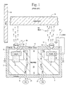
- Figures 1-2 illustrate a conventional Hall-effect, anode layer ion source.
- Figure 1 is a side cross-sectional view of an ion beam source with an ion beam emitting slit defined in the cathode
- Figure 2 is a corresponding sectional plan view along section line II--II of Figure 1
- Figure 3 is a sectional plan view similar to Figure 2 , for purposes of illustrating that the Figure 1 ion beam source may have an oval and/or racetrack-shaped ion beam emitting slit as opposed to a circular ion beam emitting slit. Any other suitable shape may also be used.
- the ion source includes a hollow housing made of a highly magnetoconductive (or permeable) material such as iron, which is used as a cathode 5.
- Cathode 5 includes cylindrical or oval side wall 7, a closed or partially closed bottom wall 9, and an approximately flat top wall 11 in which a circular or oval ion emitting slit and/or aperture 15 is defined.
- the bottom 9 and side wall(s) 7 of the cathode are optional.
- Ion emitting slit/aperture 15 includes an inner periphery as well as an outer periphery.
- Deposition and/or plasma maintenance gas supply aperture or hole(s) 21 is/are formed in bottom wall 9.
- Flat top wall 11 functions as an accelerating electrode.
- a magnetic system including a cylindrical permanent magnet 23 with poles N and S of opposite polarity is placed inside the housing between bottom wall 9 and top wall 11.
- the purpose of the magnetic system with a closed magnetic circuit formed by the magnet 23 and cathode 5 is to induce a substantially transverse magnetic field (MF) in an area proximate ion emitting slit 15.
- the ion source may be entirely or partially within wall 50. In certain instances, wall 50 may entirely surround the source and substrate 45, while in other instances the wall 50 may only partially surround the ion source and/or substrate.
- a circular or oval shaped conductive anode 25, electrically connected to the positive pole of electric power source 29, is arranged so as to at least partially surround magnet 23 and be approximately concentric therewith.
- Anode 25 may be fixed inside the housing by way of insulative ring 31 (e.g., of ceramic).
- Anode 25 defines a central opening therein in which magnet 23 is located.
- the negative pole of electric power source 29 is connected to cathode 5, so that the cathode is negative with respect to the anode (e.g., the cathode may be grounded).
- Fig. 1 illustrates that portions of both the inner and outer cathode 5 portions overhang parts of the anode 25, thereby creating areas of overhang OH.
- the anode 25 is generally biased positive by several hundred to a few thousand volts.
- the cathode (the term “cathode” as used herein includes the inner and/or outer portions thereof) is generally held at, or close to, ground potential. This is the case during all aspects of source operation, including during a mode in which the source is being cleaned.
- the conventional ion beam source of Figures 1-3 is intended for the formation of a unilaterally directed tubular (in the case of a standard beam collimated mode for example) ion beam, flowing in the direction toward substrate 45.
- Substrate 45 may or may not be biased in different instances.
- the ion beam emitted from the area of slit/aperture 15 is in the form of a circle in the Figure 2 embodiment and in the form of an oval (e.g., race-track) in the Figure 3 embodiment.
- the conventional ion beam source of Figures 1-3 operates as follows in a depositing mode when it is desired to ion beam deposit a layer(s) on substrate 45.
- a vacuum chamber in which the substrate 45 and slit/aperture 15 are located is evacuated to a pressure less than atmospheric, and a depositing gas (e.g., a hydrocarbon gas such as acetylene, or the like) is fed into the interior of the source via gas aperture(s) 21 or in any other suitable manner.
- a maintenance gas e.g., argon
- Power supply 29 is activated and an electric field is generated between anode 25 and cathode 5, which accelerates electrons to high energy.
- Anode 25 is positively biased by several hundred to a few thousand volts, and cathode 5 is at ground potential or proximate thereto as shown in Fig. 1 . Electron collisions with the gas in or proximate aperture/slit 15 leads to ionization and plasma is generated.
- "Plasma” herein means a cloud of gas including ions of a material to be accelerated toward substrate 45. The plasma expands and fills (or at least partially fills) a region including slit/aperture 15. An electric field is produced in slit 15, oriented in the direction substantially perpendicular to the transverse magnetic field, which causes the ions to propagate toward substrate 45.
- Electrons in the ion acceleration space in and/or proximate slit/aperture 15 are propelled by the known E x B drift (Hall current) in a closed loop path within the region of crossed electric and magnetic field lines proximate slit/aperture 15. These circulating electrons contribute to ionization of the gas (the term "gas” as used herein means at least one gas), so that the zone of ionizing collisions extends beyond the electrical gap between the anode and cathode and includes the region proximate slit/aperture 15 on one and/or both sides of the cathode 5.
- gas the term "gas” as used herein means at least one gas
- silane and/or acetylene (C 2 H 2 ) depositing gas is/are utilized by the ion source of Figures 1-3 in a depositing mode.
- the silane and/or acetylene depositing gas passes through the gap between anode 25 and cathode 5.
- certain of the elements in acetylene and/or silane gas is/are insulative in nature (e.g., carbide may be an insulator in certain applications).
- Insulating deposits e.g., carbide deposits, carbon deposits, and/or oxide deposits which may be insulating or semi-insulating in nature
- Insulating deposits can quickly build up on the respective surfaces of anode 25 and/or cathode 5 proximate the gap therebetween, and/or at other electrode locations.
- Insulating deposits e.g., carbide deposits, carbon deposits, and/or oxide deposits which may be insulating or semi-insulating in nature
- An ion source according to the present invention is defined in present claim 1. Since no areas of overhang are provided between the anode and the inner and outer cathode portion, there is less undesirable build-up on the anode and/or cathode during operation of the ion source so that the source can run more efficiently. Moreover, in certain example embodiments, an insulator such as a ceramic or the like is provided between the anode and cathode.
- this substantially planar design where there is no area of overhang between the anode/cathode on the side of the ion source facing the substrate, is advantageous in that: (a) it permits high current operation at low potential thereby yielding a high flux of potentially low energy ions toward the substrate; (b) the lack or reduction of overhang areas or interior spaces between the anode/cathode reducing the amount of undesirable build-ups on the anode and/or cathode during source operation and thus reduces the required frequency of cleaning and/or duty cycle of the source; and/or (c) it creates an ion source which optimizes the effectiveness of a magnetron mode of cleaning.
- FIGURE 1 is a schematic partial cross sectional view of a conventional cold cathode closed drift ion source.
- FIGURE 2 is a sectional view taken along section line II of Fig. 1 .
- FIGURE 3 is a sectional view similar to Fig. 2 , taken along section line II in Fig. 1 , in another embodiment illustrating that the ion source may be shaped in an oval manner instead of in a circular manner in certain instances.
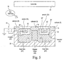
- FIGURE 4 is a perspective partial cross sectional view of part of an ion source according to an example embodiment of this invention.
- FIGURE 5 is a cross sectional view of the ion source of Fig. 4 .
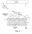
- FIGURE 6 is a cross sectional view of an ion source according to another example embodiment of this invention.
- Certain example embodiments of this invention relate to an ion source having a substantially planar design so that the anode is not substantially overlapped by the inner and outer cathode portion.
- This design is optimized in certain example embodiments for high pressure operation in a manner similar to that known as a diffused mode of operation in a closed-drift, Hall-effect, ion source.
- the ion source in certain example embodiments is a cold cathode closed drift ion source.
- Operating pressures may be below atmospheric pressure, and may be similar to those of planar and magnetron sputtering systems. In view of example designed discussed herein, high current operation at low potential yielding a high flux of low energy ions toward the substrate is possible.
- Another example advantage is the lack of interior free unoccupied space between the anode and cathode, which results in less undesirable material build-ups on the anode/cathode during source operation. Accordingly, the ion source requires less frequent cleaning and duty cycle of the source can be improved. Still further, the ion source is much easier to clean due to designs of certain example embodiments of this invention.
- the substantially planar design may optimize the effectiveness of magnetron mode cleaning of the ion source where both the anode and cathode of the ion source are negatively biased in order to clean the same.
- manual cleaning during a vent cycle will not necessarily require disassembly of the ion source.
- Fig. 4 is a perspective and partial cross sectional view of an ion source according to an example embodiment of this invention
- Fig. 5 is a side cross-sectional view of the ion source of Fig. 4
- the ion source includes a hollow housing 20 made of a highly magnetoconductive material such as low carbon steel, iron, or any other suitable material.
- This housing may or may not be used as the cathode in certain example embodiments.
- the cathode may include body 20 in certain example embodiments and may not in other example embodiments.
- the ion source in a plane proximate the side of the ion source closest to the substrate, includes conductive cathode 5 which includes both inner cathode portion 5a and outer cathode portion 5b.
- the outer cathode portion 5b surrounds or substantially surrounds the inner cathode portion 5a in certain example embodiments of this invention, and the two may be coaxial in certain example instances.
- the inner and outer cathodes may be of the same conductive material in certain embodiments, although this invention is not so limited unless expressly claimed.
- the cathode portions may be circular or oval shaped in different example embodiments of this invention (e.g., see Figs. 2-3 ).
- an ion emitting gap 22 which includes an inner periphery defined by the periphery of the inner cathode portion 5a and an outer periphery defined by the inner periphery of the outer cathode portion 5b.
- the ion source of Figs. 4-5 further includes conductive anode 25 of a material such as stainless steel or any other suitable conductive material.
- anode 25 is either circular shaped or oval shaped as viewed from above or below, and may be coaxial and/or concentric with the inner and/or outer cathode 5 portions. As viewed from above and/or below, the anode 25 is located between the inner and outer portions (5a and 5b) of the cathode 5 immediately adjacent the ion emitting gap 22, so that a bottom side of the ion emitting gap 22 is defined by the upper surface 25' of the anode 25.
- Gas such as argon and/or a hydrocarbon gas like acetylene may be introduced into the ion source via the vacuum/depositing chamber between the source and the substrate as described, for example and without limitation, in US Patent No. Re 38,358 and/or US Patent Application No. 2004/0074444 .
- One or more gas inlets may be used to introduce one or more gases from one or more gas sources 30.
- An inert gas such as argon or the like may be introduced to the source in such a manner when the ion source is to be used to clean or mill a substrate, while at least a coating gas (e.g., a hydrocarbon gas such as acetylene) may be introduced to the source in such a manner when the source is to be used to deposited a coating such as diamond-like carbon (DLC) on the substrate either directly or indirectly.
- a coating gas e.g., a hydrocarbon gas such as acetylene
- DLC diamond-like carbon
- a magnetic system including a cylindrical or otherwise shaped magnet(s) 23 with poles N and S of opposite polarity is placed inside the housing under the inner cathode portion 5a, and in the aperture defined by the anode 25 as viewed from above and/or below.
- the N-pole faces the cathode portion 5a
- the S-pole faces a bottom wall of body 20.
- the purpose of the magnetic system with a closed magnetic circuit formed by the magnet(s) 23 and cathode 5 is to induce a substantially transverse magnetic field (MF) in an area proximate ion emitting slit gap 25'.
- the anode 25 is generally biased positive by several hundred to a few thousand volts.
- the cathode (the term "cathode” as used herein includes the inner and/or outer portions thereof) is generally held at, or close to, ground potential, although it may be at any potential that is negative relative to the anode.
- Figs. 4-5 illustrate that in certain embodiments of this invention, the locations of the anode 25 and cathode 5 are substantially planar so that the cathode does not overhang the anode in any respect. In other words, the areas of overhang OH shown in prior art Fig. 1 are not present in the ion source design of Figs. 4-5 .
- the inner periphery of the outer cathode portion 5b does not extend over or overlap the anode 25 in any respect as viewed from above or below, and/or the outer periphery of the inner cathode portion 5a does not extend over or overlap the anode 25 in any respect as viewed from above or below.
- This structure also permits, when viewing the source from the side as in Figs. 4-5 , at least part of the anode 25 to be located at an elevation above a bottom-most portion of the inner and/or outer cathode portions (5a and/or 5b) thereby leading to a more efficient ion emitting gap.
- the upper surface 25' of the anode 25 is located at an elevation at least as high as an area proximate a central portion of the inner cathode portion 5a as shown in Figs. 4-5 .
- the upper surface 25' of the anode 25 defines a plane which extends through a central area of the inner cathode portion 5 a.
- the upper surface of the anode 25 does not extend upwardly to an elevation as high as the upper surface of the cathode 5.
- Anode 25 is electrically insulated from cathode 5 via insulator 35, which may be of any suitable insulating material such as a ceramic.
- insulator 35 is circular or oval in shape as viewed from above and/or below, and is substantially U-shaped as viewed in cross section. From a cross sectional perspective, the anode 25 is located in the hollow of the U of the U-shaped insulator 35 as shown in Figs. 4-5 .
- Insulating material 35 may be of any suitable material, such as silicon oxide, aluminum oxide, or the like. It is noted that in alternative embodiments of this invention, a ceramic spacer is not necessary, and a dark-space gap may be used between the anode and cathodes/grounded surfaces.
- Heat sink 37 of a material such as copper is provided below the insulator 35, and the insulator 35 electrically insulates the anode 25 from the heat sink 37.
- the insulator 35 substantially surrounds at least three of the four sides of the anode 25 as viewed cross sectionally (e.g., see Figs. 4-5 ).
- the heat sink 37 substantially surrounds at least three sides of the insulator 35 as viewed cross sectionally (e.g., see Figs. 4-5 ).
- the heat sink 37 substantially surrounds at least three sides of the anode 25 as viewed cross sectionally (e.g., see Figs. 4-5 ).
- the insulative surface 35' that extends between and contacts each of the anode 25 and the cathode outer portion 5b is substantially planar and defines a plane approximately coplanar with a top surface 25' of the anode 25.
- the insulative surface 35" that extends between and contacts each of the anode 25 and the cathode inner portion 5a is substantially planar and defines a plane approximately coplanar with a top surface 25' of the anode 25.
- a side of ion emitting gap 22 is defined partially by insulative surfaces 35' and 35".
- the ion source of Figs. 4-5 may operate as follows in a depositing mode when it is desired to ion beam deposit a layer(s) on substrate 45.
- a vacuum chamber in which the substrate 45 and gap 22 are located is evacuated to a pressure less than atmospheric, and a depositing gas (e.g., a hydrocarbon gas such as acetylene, or the like) is fed into the chamber.
- a maintenance gas e.g., argon
- Power supply 29 is activated and an electric field is generated between anode 25 and cathode 5, which accelerates electrons to high energy.
- Anode 25 is positively biased by several thousand volts, and cathode 5 may be at ground potential or proximate thereto. Electron collisions with the gas in or proximate ion emitting gap 22 leads to ionization and a plasma is generated. The plasma expands and fills (or at least partially fills) a region including gap or recess 22. An electric field is produced in gap 22, oriented in the direction substantially perpendicular to the transverse magnetic field, which causes the ions to propagate toward substrate 45. Electrons in the ion acceleration space in and/or proximate gap 22 are propelled by the E x B drift in a closed loop path within the region of crossed electric and magnetic field lines proximate gap 22.
- the ions directed toward the substrate are then capable of forming, or helping form, a coating on the substrate 45 in certain example embodiments of this invention.
- the ion beam emitted from the ion source may be a diffused beam in certain example embodiments of this invention. However, in other example embodiments, the ion beam from the ion source may be focused or otherwise shaped/oriented.
- Fig. 6 is a cross sectional view of an ion source according to another example embodiment of this invention.
- the Fig. 6 embodiment is similar to the Fig. 4-5 embodiment, in that the cathode portions 5a and 5b do not overlap/overhang the anode as viewed from above and/or below.
- the upper surface of the anode 25 is flush or substantially flush with the upper surface of the cathode 5.
- the ion emitting gap 22 is formed at least partially between the inner cathode portion 5a and the outer cathode portion 5b as viewed from above or below (e.g., as viewed from the substrate).
- the magnetic stack 23 is illustrated in the center of the source. However, this need not be the case in alternative embodiments, as the central location is used for convenience only and is not a requirement in all instances. It is further noted that the absolute polarity of the magnetic field (North vs. South) is not particularly important to the function of the source. Moreover, as mentioned above with respect to Figs. 4-5 , the ceramic insulator 35 of Fig. 6 may be replaced with a dark-space gap in certain alternative embodiments of this invention.
Abstract
Description
- This invention relates to an ion source having an improved design which aids in cleaning and/or operation. In certain example embodiments, the ion source comprises a substantially planar design so that there is no or substantially no area where the cathode overhangs the anode.
- An ion source is a device that causes gas molecules to be ionized and then accelerates and emits the ionized gas molecules and/or atoms toward a substrate. Such an ion source may be used for various purposes, including but not limited to cleaning a substrate, surface activation, polishing, etching, and/or deposition of thin film coatings/layer(s). Example ion sources are disclosed, for example, in
U.S. Patent Nos. 6,359,388 ;6,037,717 ;6,002,208 ; and5,656,819 .US-2004/0074444 discloses an ion source as difined in the preamble of present claim 1. -
Figures 1-2 illustrate a conventional Hall-effect, anode layer ion source. In particular,Figure 1 is a side cross-sectional view of an ion beam source with an ion beam emitting slit defined in the cathode, andFigure 2 is a corresponding sectional plan view along section line II--II ofFigure 1 .Figure 3 is a sectional plan view similar toFigure 2 , for purposes of illustrating that theFigure 1 ion beam source may have an oval and/or racetrack-shaped ion beam emitting slit as opposed to a circular ion beam emitting slit. Any other suitable shape may also be used. - Referring to
Figures 1-3 , the ion source includes a hollow housing made of a highly magnetoconductive (or permeable) material such as iron, which is used as acathode 5. Cathode 5 includes cylindrical oroval side wall 7, a closed or partially closedbottom wall 9, and an approximatelyflat top wall 11 in which a circular or oval ion emitting slit and/oraperture 15 is defined. Thebottom 9 and side wall(s) 7 of the cathode are optional. Ion emitting slit/aperture 15 includes an inner periphery as well as an outer periphery. - Deposition and/or plasma maintenance gas supply aperture or hole(s) 21 is/are formed in
bottom wall 9. Flattop wall 11 functions as an accelerating electrode. A magnetic system including a cylindricalpermanent magnet 23 with poles N and S of opposite polarity is placed inside the housing betweenbottom wall 9 andtop wall 11. The purpose of the magnetic system with a closed magnetic circuit formed by themagnet 23 andcathode 5 is to induce a substantially transverse magnetic field (MF) in an area proximateion emitting slit 15. The ion source may be entirely or partially withinwall 50. In certain instances,wall 50 may entirely surround the source andsubstrate 45, while in other instances thewall 50 may only partially surround the ion source and/or substrate. - A circular or oval shaped
conductive anode 25, electrically connected to the positive pole ofelectric power source 29, is arranged so as to at least partially surroundmagnet 23 and be approximately concentric therewith.Anode 25 may be fixed inside the housing by way of insulative ring 31 (e.g., of ceramic).Anode 25 defines a central opening therein in whichmagnet 23 is located. The negative pole ofelectric power source 29 is connected tocathode 5, so that the cathode is negative with respect to the anode (e.g., the cathode may be grounded).Fig. 1 illustrates that portions of both the inner andouter cathode 5 portions overhang parts of theanode 25, thereby creating areas of overhang OH. - Generally speaking, the
anode 25 is generally biased positive by several hundred to a few thousand volts. Meanwhile, the cathode (the term "cathode" as used herein includes the inner and/or outer portions thereof) is generally held at, or close to, ground potential. This is the case during all aspects of source operation, including during a mode in which the source is being cleaned. - The conventional ion beam source of
Figures 1-3 is intended for the formation of a unilaterally directed tubular (in the case of a standard beam collimated mode for example) ion beam, flowing in the direction towardsubstrate 45.Substrate 45 may or may not be biased in different instances. The ion beam emitted from the area of slit/aperture 15 is in the form of a circle in theFigure 2 embodiment and in the form of an oval (e.g., race-track) in theFigure 3 embodiment. - The conventional ion beam source of
Figures 1-3 operates as follows in a depositing mode when it is desired to ion beam deposit a layer(s) onsubstrate 45. A vacuum chamber in which thesubstrate 45 and slit/aperture 15 are located is evacuated to a pressure less than atmospheric, and a depositing gas (e.g., a hydrocarbon gas such as acetylene, or the like) is fed into the interior of the source via gas aperture(s) 21 or in any other suitable manner. A maintenance gas (e.g., argon) may also be fed into the source in certain instances, along with the depositing gas.Power supply 29 is activated and an electric field is generated betweenanode 25 andcathode 5, which accelerates electrons to high energy. Anode 25 is positively biased by several hundred to a few thousand volts, andcathode 5 is at ground potential or proximate thereto as shown inFig. 1 . Electron collisions with the gas in or proximate aperture/slit 15 leads to ionization and plasma is generated. "Plasma" herein means a cloud of gas including ions of a material to be accelerated towardsubstrate 45. The plasma expands and fills (or at least partially fills) a region including slit/aperture 15. An electric field is produced inslit 15, oriented in the direction substantially perpendicular to the transverse magnetic field, which causes the ions to propagate towardsubstrate 45. Electrons in the ion acceleration space in and/or proximate slit/aperture 15 are propelled by the known E x B drift (Hall current) in a closed loop path within the region of crossed electric and magnetic field lines proximate slit/aperture 15. These circulating electrons contribute to ionization of the gas (the term "gas" as used herein means at least one gas), so that the zone of ionizing collisions extends beyond the electrical gap between the anode and cathode and includes the region proximate slit/aperture 15 on one and/or both sides of thecathode 5. - For purposes of example, consider the situation where a silane and/or acetylene (C2H2) depositing gas is/are utilized by the ion source of
Figures 1-3 in a depositing mode. The silane and/or acetylene depositing gas passes through the gap betweenanode 25 andcathode 5. Unfortunately, certain of the elements in acetylene and/or silane gas is/are insulative in nature (e.g., carbide may be an insulator in certain applications). - Insulating deposits (e.g., carbide deposits, carbon deposits, and/or oxide deposits which may be insulating or semi-insulating in nature) resulting from the depositing gas can quickly build up on the respective surfaces of
anode 25 and/orcathode 5 proximate the gap therebetween, and/or at other electrode locations. Unfortunately, the fact that both the inner andouter cathode 5 portions overhang parts of theanode 25 as shown inFig. 1 causes even more deposits to build up on the portions of theanode 25 andcathode 5 in the areas of overhang OH. This can interfere with gas flow through the gap and/oraperture 15, and/or it can reduce net current thereby adversely affecting the electric field potential between the anode and cathode proximate slit/aperture 15. Such deposits resistively limit the amount of current that can flow through the source; this adversely interferes with the operability and/or efficiency of the ion source especially over significant lengths of time. This unfortunately can also result in micro-particles from the deposits making their way into a film being deposited on the substrate. In either case, operability and/or efficiency of the ion beam source is adversely affected. - In view of the above, it will be apparent to those skilled in the art that there exists a need for an ion beam design which leads to less undesirable build-up on the anode and/or cathode, and/or which more efficiently permits high current operation of the ion source at low potential yielding a high flux of ions toward the substrate. In certain example situations, a design that permits rapid in situ removal of build-up is also desirable.
- An ion source according to the present invention is defined in present claim 1. Since no areas of overhang are provided between the anode and the inner and outer cathode portion, there is less undesirable build-up on the anode and/or cathode during operation of the ion source so that the source can run more efficiently. Moreover, in certain example embodiments, an insulator such as a ceramic or the like is provided between the anode and cathode.
- In certain example embodiments of this invention this substantially planar design, where there is no area of overhang between the anode/cathode on the side of the ion source facing the substrate, is advantageous in that: (a) it permits high current operation at low potential thereby yielding a high flux of potentially low energy ions toward the substrate; (b) the lack or reduction of overhang areas or interior spaces between the anode/cathode reducing the amount of undesirable build-ups on the anode and/or cathode during source operation and thus reduces the required frequency of cleaning and/or duty cycle of the source; and/or (c) it creates an ion source which optimizes the effectiveness of a magnetron mode of cleaning.
- Particular embodiments of the present invention are defined in the dependent claims.
-
FIGURE 1 is a schematic partial cross sectional view of a conventional cold cathode closed drift ion source. -
FIGURE 2 is a sectional view taken along section line II ofFig. 1 . -
FIGURE 3 is a sectional view similar toFig. 2 , taken along section line II inFig. 1 , in another embodiment illustrating that the ion source may be shaped in an oval manner instead of in a circular manner in certain instances. -
FIGURE 4 is a perspective partial cross sectional view of part of an ion source according to an example embodiment of this invention. -
FIGURE 5 is a cross sectional view of the ion source ofFig. 4 . -
FIGURE 6 is a cross sectional view of an ion source according to another example embodiment of this invention. - Referring now more particularly to the accompanying drawings, in which like reference numerals indicate like parts throughout the several views. In this respect, reference numerals used in
Figs. 4-5 may be used for the same components discussed above with respect toFigs. 1-3 . - In the following description, for purposes of explanation and not limitation, specific details are set forth in order to provide an understanding of certain embodiments of the present invention. However, it will apparent to those skilled in the art that the present invention may be practiced in other embodiments that depart from these specific details. In other instances, detailed descriptions of well known devices, gases, fasteners, and other components/systems are omitted so as to not obscure the description of the present invention with unnecessary detail.
- Certain example embodiments of this invention relate to an ion source having a substantially planar design so that the anode is not substantially overlapped by the inner and outer cathode portion. This design is optimized in certain example embodiments for high pressure operation in a manner similar to that known as a diffused mode of operation in a closed-drift, Hall-effect, ion source. In this respect, the ion source in certain example embodiments is a cold cathode closed drift ion source. Operating pressures may be below atmospheric pressure, and may be similar to those of planar and magnetron sputtering systems. In view of example designed discussed herein, high current operation at low potential yielding a high flux of low energy ions toward the substrate is possible. Another example advantage is the lack of interior free unoccupied space between the anode and cathode, which results in less undesirable material build-ups on the anode/cathode during source operation. Accordingly, the ion source requires less frequent cleaning and duty cycle of the source can be improved. Still further, the ion source is much easier to clean due to designs of certain example embodiments of this invention.
- Moreover, in certain example embodiments of this invention, the substantially planar design may optimize the effectiveness of magnetron mode cleaning of the ion source where both the anode and cathode of the ion source are negatively biased in order to clean the same. As another example advantage, manual cleaning during a vent cycle will not necessarily require disassembly of the ion source.
-
Fig. 4 is a perspective and partial cross sectional view of an ion source according to an example embodiment of this invention, andFig. 5 is a side cross-sectional view of the ion source ofFig. 4 . Referring toFigs. 4-5 , the ion source includes ahollow housing 20 made of a highly magnetoconductive material such as low carbon steel, iron, or any other suitable material. This housing may or may not be used as the cathode in certain example embodiments. In other words, the cathode may includebody 20 in certain example embodiments and may not in other example embodiments. - The ion source, in a plane proximate the side of the ion source closest to the substrate, includes
conductive cathode 5 which includes bothinner cathode portion 5a andouter cathode portion 5b. Theouter cathode portion 5b surrounds or substantially surrounds theinner cathode portion 5a in certain example embodiments of this invention, and the two may be coaxial in certain example instances. The inner and outer cathodes may be of the same conductive material in certain embodiments, although this invention is not so limited unless expressly claimed. The cathode portions may be circular or oval shaped in different example embodiments of this invention (e.g., seeFigs. 2-3 ). Between the inner andouter cathode portions ion emitting gap 22 which includes an inner periphery defined by the periphery of theinner cathode portion 5a and an outer periphery defined by the inner periphery of theouter cathode portion 5b. - The ion source of
Figs. 4-5 further includesconductive anode 25 of a material such as stainless steel or any other suitable conductive material. In certain example embodiments,anode 25 is either circular shaped or oval shaped as viewed from above or below, and may be coaxial and/or concentric with the inner and/orouter cathode 5 portions. As viewed from above and/or below, theanode 25 is located between the inner and outer portions (5a and 5b) of thecathode 5 immediately adjacent theion emitting gap 22, so that a bottom side of theion emitting gap 22 is defined by the upper surface 25' of theanode 25. - Gas such as argon and/or a hydrocarbon gas like acetylene may be introduced into the ion source via the vacuum/depositing chamber between the source and the substrate as described, for example and without limitation, in
US Patent No. Re 38,358 and/orUS Patent Application No. 2004/0074444 . One or more gas inlets (not shown) may be used to introduce one or more gases from one ormore gas sources 30. An inert gas such as argon or the like may be introduced to the source in such a manner when the ion source is to be used to clean or mill a substrate, while at least a coating gas (e.g., a hydrocarbon gas such as acetylene) may be introduced to the source in such a manner when the source is to be used to deposited a coating such as diamond-like carbon (DLC) on the substrate either directly or indirectly. - A magnetic system including a cylindrical or otherwise shaped magnet(s) 23 with poles N and S of opposite polarity is placed inside the housing under the
inner cathode portion 5a, and in the aperture defined by theanode 25 as viewed from above and/or below. In certain example embodiments, the N-pole faces thecathode portion 5a, while the S-pole faces a bottom wall ofbody 20. The purpose of the magnetic system with a closed magnetic circuit formed by the magnet(s) 23 andcathode 5 is to induce a substantially transverse magnetic field (MF) in an area proximate ion emitting slit gap 25'. Generally speaking, theanode 25 is generally biased positive by several hundred to a few thousand volts. Meanwhile, the cathode (the term "cathode" as used herein includes the inner and/or outer portions thereof) is generally held at, or close to, ground potential, although it may be at any potential that is negative relative to the anode. -
Figs. 4-5 illustrate that in certain embodiments of this invention, the locations of theanode 25 andcathode 5 are substantially planar so that the cathode does not overhang the anode in any respect. In other words, the areas of overhang OH shown in prior artFig. 1 are not present in the ion source design ofFigs. 4-5 . As shown inFigs. 4-5 , in certain example embodiments of this invention, the inner periphery of theouter cathode portion 5b does not extend over or overlap theanode 25 in any respect as viewed from above or below, and/or the outer periphery of theinner cathode portion 5a does not extend over or overlap theanode 25 in any respect as viewed from above or below. This structure also permits, when viewing the source from the side as inFigs. 4-5 , at least part of theanode 25 to be located at an elevation above a bottom-most portion of the inner and/or outer cathode portions (5a and/or 5b) thereby leading to a more efficient ion emitting gap. In certain example embodiments, the upper surface 25' of theanode 25 is located at an elevation at least as high as an area proximate a central portion of theinner cathode portion 5a as shown inFigs. 4-5 . In certain example embodiments, the upper surface 25' of theanode 25 defines a plane which extends through a central area of theinner cathode portion 5 a. - However, in certain example embodiments of this invention, the upper surface of the
anode 25 does not extend upwardly to an elevation as high as the upper surface of thecathode 5. As a result, there is a slight depression or recess formed in the top surface of the ion source between 5a, 5b and 25. This recess forms at least part of theion emitting gap 22 discussed herein. -
Anode 25 is electrically insulated fromcathode 5 viainsulator 35, which may be of any suitable insulating material such as a ceramic. In the illustrated example embodiment,insulator 35 is circular or oval in shape as viewed from above and/or below, and is substantially U-shaped as viewed in cross section. From a cross sectional perspective, theanode 25 is located in the hollow of the U of theU-shaped insulator 35 as shown inFigs. 4-5 . Insulatingmaterial 35 may be of any suitable material, such as silicon oxide, aluminum oxide, or the like. It is noted that in alternative embodiments of this invention, a ceramic spacer is not necessary, and a dark-space gap may be used between the anode and cathodes/grounded surfaces.Heat sink 37 of a material such as copper is provided below theinsulator 35, and theinsulator 35 electrically insulates theanode 25 from theheat sink 37. In certain example embodiments of this invention, theinsulator 35 substantially surrounds at least three of the four sides of theanode 25 as viewed cross sectionally (e.g., seeFigs. 4-5 ). Moreover, in certain example embodiments, theheat sink 37 substantially surrounds at least three sides of theinsulator 35 as viewed cross sectionally (e.g., seeFigs. 4-5 ). Likewise, in certain example embodiments, theheat sink 37 substantially surrounds at least three sides of theanode 25 as viewed cross sectionally (e.g., seeFigs. 4-5 ). - As shown in
Figs. 4-5 , in certain example embodiments of this invention, the insulative surface 35' that extends between and contacts each of theanode 25 and the cathodeouter portion 5b is substantially planar and defines a plane approximately coplanar with a top surface 25' of theanode 25. Moreover, in certain example embodiments of this invention, theinsulative surface 35" that extends between and contacts each of theanode 25 and the cathodeinner portion 5a is substantially planar and defines a plane approximately coplanar with a top surface 25' of theanode 25. A side ofion emitting gap 22 is defined partially byinsulative surfaces 35' and 35". - Advantageously, high current operation at low potential yielding a high flux of low energy ions toward the substrate is possible; this is sometimes desirable in ion assisted deposition applications or the like. Another example advantage is the lack of interior free unoccupied space between the anode and cathode, which results in less undesirable material build-ups on the anode/cathode during source operation and thus more efficient ion source operation and less frequent cleaning being needed.
- For purposes of example and without limitation, the ion source of
Figs. 4-5 may operate as follows in a depositing mode when it is desired to ion beam deposit a layer(s) onsubstrate 45. A vacuum chamber in which thesubstrate 45 andgap 22 are located is evacuated to a pressure less than atmospheric, and a depositing gas (e.g., a hydrocarbon gas such as acetylene, or the like) is fed into the chamber. A maintenance gas (e.g., argon) may also be fed into the chamber, along with the depositing gas.Power supply 29 is activated and an electric field is generated betweenanode 25 andcathode 5, which accelerates electrons to high energy.Anode 25 is positively biased by several thousand volts, andcathode 5 may be at ground potential or proximate thereto. Electron collisions with the gas in or proximateion emitting gap 22 leads to ionization and a plasma is generated. The plasma expands and fills (or at least partially fills) a region including gap orrecess 22. An electric field is produced ingap 22, oriented in the direction substantially perpendicular to the transverse magnetic field, which causes the ions to propagate towardsubstrate 45. Electrons in the ion acceleration space in and/orproximate gap 22 are propelled by the E x B drift in a closed loop path within the region of crossed electric and magnetic field linesproximate gap 22. These circulating electrons contribute to ionization of the gas, so that the zone of ionizing collisions extends beyond the electrical gap between the anode and cathode and includes the regionproximate gap 22 on one and/or both sides of thecathode 5. The ions directed toward the substrate are then capable of forming, or helping form, a coating on thesubstrate 45 in certain example embodiments of this invention. - The ion beam emitted from the ion source may be a diffused beam in certain example embodiments of this invention. However, in other example embodiments, the ion beam from the ion source may be focused or otherwise shaped/oriented.
-
Fig. 6 is a cross sectional view of an ion source according to another example embodiment of this invention. TheFig. 6 embodiment is similar to theFig. 4-5 embodiment, in that thecathode portions Fig. 6 embodiment, the upper surface of theanode 25 is flush or substantially flush with the upper surface of thecathode 5. In theFig. 6 embodiment, as in theFig. 4-5 embodiment, theion emitting gap 22 is formed at least partially between theinner cathode portion 5a and theouter cathode portion 5b as viewed from above or below (e.g., as viewed from the substrate). - In the aforesaid embodiments it is noted that the
magnetic stack 23 is illustrated in the center of the source. However, this need not be the case in alternative embodiments, as the central location is used for convenience only and is not a requirement in all instances. It is further noted that the absolute polarity of the magnetic field (North vs. South) is not particularly important to the function of the source. Moreover, as mentioned above with respect toFigs. 4-5 , theceramic insulator 35 ofFig. 6 may be replaced with a dark-space gap in certain alternative embodiments of this invention. - While the invention has been described in connection with what is presently considered to be the most practical and preferred embodiment, it is to be understood that the invention is not to be limited to the disclosed embodiment, but on the contrary, is intended to cover various modifications within the scope of the appended claims.
Claims (21)
- An ion source comprising:a conductive cathode comprising an inner cathode portion (5a) and an outer cathode portion (5b) in a given plane;an ion emitting gap (22), formed at least partially between the inner cathode portion and the outer cathode portion, which includes an inner periphery defined by the periphery of the inner cathode portion (5a) and an outer periphery defined by the inner periphery of the outer cathode portion (5b); an anode (25) located between the inner cathode portion (5a) and the outer cathode portion (5b) as viewed from perpendicular above and/or below the given plane;characterized in that no portion of the inner cathode portion (5a) overlaps the anode (25), and no portion of the outer cathode portion (5b) overlaps the anode (25) as viewed from perpendicular above and/or below the given plane.
- The ion source of claim 1, wherein an upper surface of the anode (25) defines a plane which extends through a central portion of at least the inner cathode portion (5a).
- The ion source of claim 1, wherein an area between the anode (25) and the cathode (5) is provided with a ceramic insulator (35).
- The ion source of claim 1, wherein an insulative surface extending between and contacting the anode and the inner cathode portion is coplanar with an upper surface of the anode.
- The ion source of claim 1, wherein an insulative surface extending between and contacting the anode and the outer cathode portion is coplanar with an upper surface of the anode.
- The ion source of claim 1, further comprising at least one magnet (23) at least partially located adjacent the inner cathode portion (5a) and located in an aperture defined in the anode (25) as viewed from above and/or below.
- The ion source of claim 1, wherein a recess is defined on a side of the ion source closest to a substrate toward which ions from the source are to be directed, and wherein the recess is at least partially defined by each of the anode (25) and cathode (5).
- The ion source of claim 7, wherein the ion emitting gap (22) of the ion source is at least partially defined by the recess.
- The ion source of claim 7, wherein a bottom side of the recess has no air gap and is formed by a continuous surface including surfaces of the anode, cathode and an insulator.
- The ion source of claim 1, further comprising an insulator (35) which surrounds three sides of the anode as viewed cross sectionally.
- The ion source of claim 1, further comprising a heat sink (37) which surrounds three sides of the anode (25) as viewed cross sectionally.
- The ion source of claim 1, wherein the ion source is a cold cathode closed drift ion source.
- The ion source of claim 1, wherein the inner cathode portion (5a) and the outer cathode portion (5b) are of the same conductive material.
- The ion source of claim 1, wherein gas is introduced to the ion source from a side thereof closest to a substrate toward which ions from the source are to be directed.
- The ion source of claim 1, wherein an upper surface of the anode is substantially coplanar with an upper surface of the cathode.
- An ion source according to claim 1, wherein at least part of the anode (25) is located at an elevation above a bottom-most portion of the inner cathode portion (5a) and/or the outer cathode portion (5b), so that at least part of the anode (25) is located directly between the inner cathode portion (5a) and the outer cathode portion (5b).
- The ion source of claim 16, wherein an upper surface of the anode defines a plane which extends through a central portion of at least the inner cathode portion.
- The ion source of claim 16, wherein an upper surface of the anode is substantially coplanar with an upper surface of the cathode.
- The ion source of claim 16, wherein an area between the anode and the cathode is provided with a ceramic insulator.
- The ion source of claim 16, wherein an insulative surface extending between and contacting the anode and the inner cathode portion is coplanar with an upper surface of the anode and/or an upper surface of the cathode.
- The ion source of claim 16, wherein an insulative surface extending between and contacting the anode and the outer cathode portion is coplanar with an upper surface of the anode.
Priority Applications (1)
| Application Number | Priority Date | Filing Date | Title |
|---|---|---|---|
| PL05818170T PL1825491T3 (en) | 2004-11-12 | 2005-11-07 | Ion source with substantially planar design |
Applications Claiming Priority (2)
| Application Number | Priority Date | Filing Date | Title |
|---|---|---|---|
| US10/986,456 US7183559B2 (en) | 2004-11-12 | 2004-11-12 | Ion source with substantially planar design |
| PCT/US2005/040159 WO2006055296A2 (en) | 2004-11-12 | 2005-11-07 | Ion source with substantially planar design |
Publications (2)
| Publication Number | Publication Date |
|---|---|
| EP1825491A2 EP1825491A2 (en) | 2007-08-29 |
| EP1825491B1 true EP1825491B1 (en) | 2008-09-24 |
Family
ID=36010910
Family Applications (1)
| Application Number | Title | Priority Date | Filing Date |
|---|---|---|---|
| EP05818170A Not-in-force EP1825491B1 (en) | 2004-11-12 | 2005-11-07 | Ion source with substantially planar design |
Country Status (8)
| Country | Link |
|---|---|
| US (1) | US7183559B2 (en) |
| EP (1) | EP1825491B1 (en) |
| AT (1) | ATE409355T1 (en) |
| CA (1) | CA2585176C (en) |
| DE (1) | DE602005009972D1 (en) |
| ES (1) | ES2313443T3 (en) |
| PL (1) | PL1825491T3 (en) |
| WO (1) | WO2006055296A2 (en) |
Families Citing this family (24)
| Publication number | Priority date | Publication date | Assignee | Title |
|---|---|---|---|---|
| TWI259491B (en) * | 2004-12-24 | 2006-08-01 | Ind Tech Res Inst | Improved anode layer particle beam device |
| US7405411B2 (en) * | 2005-05-06 | 2008-07-29 | Guardian Industries Corp. | Ion source with multi-piece outer cathode |
| US7872422B2 (en) * | 2006-07-18 | 2011-01-18 | Guardian Industries Corp. | Ion source with recess in electrode |
| US7550927B2 (en) * | 2006-11-09 | 2009-06-23 | Applied Materials, Inc. | System and method for generating ions and radicals |
| US20120015195A1 (en) | 2007-01-29 | 2012-01-19 | Guardian Industries Corp. and C.R.V.C. | Method of making heat treated and ion-beam etched/milled coated article using diamond-like carbon (dlc) coating and protective film |
| US20120040160A1 (en) | 2007-01-29 | 2012-02-16 | Guardian Industries Corp. | Method of making heat treated and ion-beam etched/milled coated article using diamond-like carbon (dlc) protective film |
| US20120015196A1 (en) | 2007-01-29 | 2012-01-19 | Guardian Industries Corp. | Method of making heat treated coated article using diamond-like carbon (dlc) coating and protective film on acid-etched surface |
| KR100838045B1 (en) * | 2007-11-28 | 2008-06-12 | 심문식 | Sputtering and ion beam deposition |
| US9136086B2 (en) * | 2008-12-08 | 2015-09-15 | General Plasma, Inc. | Closed drift magnetic field ion source apparatus containing self-cleaning anode and a process for substrate modification therewith |
| US10586689B2 (en) | 2009-07-31 | 2020-03-10 | Guardian Europe S.A.R.L. | Sputtering apparatus including cathode with rotatable targets, and related methods |
| US20120187843A1 (en) * | 2009-08-03 | 2012-07-26 | Madocks John E | Closed drift ion source with symmetric magnetic field |
| US20110100446A1 (en) | 2009-11-05 | 2011-05-05 | Guardian Industries Corp. | High haze transparent contact including ion-beam treated layer for solar cells, and/or method of making the same |
| US20110186120A1 (en) * | 2009-11-05 | 2011-08-04 | Guardian Industries Corp. | Textured coating with various feature sizes made by using multiple-agent etchant for thin-film solar cells and/or methods of making the same |
| US8502066B2 (en) * | 2009-11-05 | 2013-08-06 | Guardian Industries Corp. | High haze transparent contact including insertion layer for solar cells, and/or method of making the same |
| US20110168252A1 (en) | 2009-11-05 | 2011-07-14 | Guardian Industries Corp. | Textured coating with etching-blocking layer for thin-film solar cells and/or methods of making the same |
| EP2431995A1 (en) * | 2010-09-17 | 2012-03-21 | Asociacion de la Industria Navarra (AIN) | Ionisation device |
| US8541792B2 (en) | 2010-10-15 | 2013-09-24 | Guardian Industries Corp. | Method of treating the surface of a soda lime silica glass substrate, surface-treated glass substrate, and device incorporating the same |
| US20120167971A1 (en) | 2010-12-30 | 2012-07-05 | Alexey Krasnov | Textured coating for thin-film solar cells and/or methods of making the same |
| WO2013019129A2 (en) * | 2011-08-03 | 2013-02-07 | Institute Of Geological And Nuclear Sciences Limited | Ion source |
| WO2014175702A1 (en) * | 2013-04-26 | 2014-10-30 | (주) 화인솔루션 | Ion beam source |
| KR101480114B1 (en) * | 2013-06-13 | 2015-01-07 | (주)화인솔루션 | Ion Source with Sealing and Fixing Insulator |
| US20210147974A1 (en) * | 2017-06-08 | 2021-05-20 | Board Of Trustees Of Michigan State University | Magnetic-field-assisted plasma coating system |
| CN108914091B (en) * | 2018-08-10 | 2020-09-01 | 成都极星等离子科技有限公司 | Improved anode layer ion source |
| CN110846624B (en) * | 2019-11-07 | 2022-10-04 | 北京大学深圳研究生院 | Anode layer ion source |
Family Cites Families (21)
| Publication number | Priority date | Publication date | Assignee | Title |
|---|---|---|---|---|
| US38358A (en) * | 1863-04-28 | Improvement in em b roidering-m ach ines | ||
| US5656819A (en) | 1994-11-16 | 1997-08-12 | Sandia Corporation | Pulsed ion beam source |
| US6002208A (en) | 1998-07-02 | 1999-12-14 | Advanced Ion Technology, Inc. | Universal cold-cathode type ion source with closed-loop electron drifting and adjustable ion-emitting slit |
| US6147354A (en) * | 1998-07-02 | 2000-11-14 | Maishev; Yuri | Universal cold-cathode type ion source with closed-loop electron drifting and adjustable ionization gap |
| US6153067A (en) | 1998-12-30 | 2000-11-28 | Advanced Ion Technology, Inc. | Method for combined treatment of an object with an ion beam and a magnetron plasma with a combined magnetron-plasma and ion-beam source |
| US6037717A (en) | 1999-01-04 | 2000-03-14 | Advanced Ion Technology, Inc. | Cold-cathode ion source with a controlled position of ion beam |
| US6242749B1 (en) * | 1999-01-30 | 2001-06-05 | Yuri Maishev | Ion-beam source with uniform distribution of ion-current density on the surface of an object being treated |
| US6246059B1 (en) * | 1999-03-06 | 2001-06-12 | Advanced Ion Technology, Inc. | Ion-beam source with virtual anode |
| WO2000063459A1 (en) | 1999-04-17 | 2000-10-26 | Advanced Energy Industries, Inc. | Method and apparatus for deposition of diamond like carbon |
| US6740211B2 (en) | 2001-12-18 | 2004-05-25 | Guardian Industries Corp. | Method of manufacturing windshield using ion beam milling of glass substrate(s) |
| US6368664B1 (en) | 1999-05-03 | 2002-04-09 | Guardian Industries Corp. | Method of ion beam milling substrate prior to depositing diamond like carbon layer thereon |
| EP1282909A1 (en) * | 1999-08-02 | 2003-02-12 | Advanced Energy Industries, Inc. | Enhanced electron emissive surfaces for a thin film deposition system using ion sources |
| US6359388B1 (en) | 2000-08-28 | 2002-03-19 | Guardian Industries Corp. | Cold cathode ion beam deposition apparatus with segregated gas flow |
| US6919672B2 (en) * | 2002-04-10 | 2005-07-19 | Applied Process Technologies, Inc. | Closed drift ion source |
| US6815690B2 (en) * | 2002-07-23 | 2004-11-09 | Guardian Industries Corp. | Ion beam source with coated electrode(s) |
| US6988463B2 (en) * | 2002-10-18 | 2006-01-24 | Guardian Industries Corp. | Ion beam source with gas introduced directly into deposition/vacuum chamber |
| US6812648B2 (en) * | 2002-10-21 | 2004-11-02 | Guardian Industries Corp. | Method of cleaning ion source, and corresponding apparatus/system |
| US6806651B1 (en) * | 2003-04-22 | 2004-10-19 | Zond, Inc. | High-density plasma source |
| US7718983B2 (en) * | 2003-08-20 | 2010-05-18 | Veeco Instruments, Inc. | Sputtered contamination shielding for an ion source |
| WO2005024880A2 (en) * | 2003-09-03 | 2005-03-17 | Guardian Industries Corp. | Floating mode ion source |
| US7030390B2 (en) * | 2003-09-09 | 2006-04-18 | Guardian Industries Corp. | Ion source with electrode kept at potential(s) other than ground by zener diode(s), thyristor(s) and/or the like |
-
2004
- 2004-11-12 US US10/986,456 patent/US7183559B2/en not_active Expired - Fee Related
-
2005
- 2005-11-07 DE DE602005009972T patent/DE602005009972D1/en active Active
- 2005-11-07 WO PCT/US2005/040159 patent/WO2006055296A2/en active Application Filing
- 2005-11-07 PL PL05818170T patent/PL1825491T3/en unknown
- 2005-11-07 ES ES05818170T patent/ES2313443T3/en active Active
- 2005-11-07 AT AT05818170T patent/ATE409355T1/en not_active IP Right Cessation
- 2005-11-07 CA CA2585176A patent/CA2585176C/en not_active Expired - Fee Related
- 2005-11-07 EP EP05818170A patent/EP1825491B1/en not_active Not-in-force
Also Published As
| Publication number | Publication date |
|---|---|
| EP1825491A2 (en) | 2007-08-29 |
| DE602005009972D1 (en) | 2008-11-06 |
| US7183559B2 (en) | 2007-02-27 |
| WO2006055296A2 (en) | 2006-05-26 |
| CA2585176A1 (en) | 2006-05-26 |
| PL1825491T3 (en) | 2009-03-31 |
| WO2006055296A3 (en) | 2006-08-31 |
| ES2313443T3 (en) | 2009-03-01 |
| US20060103319A1 (en) | 2006-05-18 |
| CA2585176C (en) | 2010-08-10 |
| ATE409355T1 (en) | 2008-10-15 |
Similar Documents
| Publication | Publication Date | Title |
|---|---|---|
| EP1825491B1 (en) | Ion source with substantially planar design | |
| EP2057300B1 (en) | Ion source with recess in electrode | |
| EP1894221B1 (en) | Ion source with multi-piece outer cathode | |
| US6812648B2 (en) | Method of cleaning ion source, and corresponding apparatus/system | |
| US6359388B1 (en) | Cold cathode ion beam deposition apparatus with segregated gas flow | |
| JP3775689B2 (en) | Method and apparatus for ionizing sputtering of materials | |
| US6254745B1 (en) | Ionized physical vapor deposition method and apparatus with magnetic bucket and concentric plasma and material source | |
| JP3603024B2 (en) | Ionization physical vapor deposition method and apparatus therefor | |
| KR100659828B1 (en) | Method and apparatus for ionized physical vapor deposition | |
| US6197165B1 (en) | Method and apparatus for ionized physical vapor deposition | |
| KR101146071B1 (en) | Magnetically enhanced capacitive plasma source for ionized physical vapor deposition | |
| US6987364B2 (en) | Floating mode ion source | |
| US6224725B1 (en) | Unbalanced magnetron sputtering with auxiliary cathode | |
| US6988463B2 (en) | Ion beam source with gas introduced directly into deposition/vacuum chamber | |
| US6184625B1 (en) | Ion beam processing apparatus for processing work piece with ion beam being neutralized uniformly | |
| US8377269B2 (en) | Sputtering apparatus | |
| WO2000003055A1 (en) | Shield for ionized physical vapor deposition apparatus | |
| US20220013324A1 (en) | Single beam plasma source | |
| JP2005290442A (en) | Ecr sputtering system | |
| JPH0575951U (en) | Ion source |
Legal Events
| Date | Code | Title | Description |
|---|---|---|---|
| PUAI | Public reference made under article 153(3) epc to a published international application that has entered the european phase |
Free format text: ORIGINAL CODE: 0009012 |
|
| 17P | Request for examination filed |
Effective date: 20070510 |
|
| AK | Designated contracting states |
Kind code of ref document: A2 Designated state(s): AT BE BG CH CY CZ DE DK EE ES FI FR GB GR HU IE IS IT LI LT LU LV MC NL PL PT RO SE SI SK TR |
|
| RIN1 | Information on inventor provided before grant (corrected) |
Inventor name: LUTEN, HENRY, A. Inventor name: VEERASAMY, VIJAYEN, S. |
|
| RIN1 | Information on inventor provided before grant (corrected) |
Inventor name: VEERASAMY, VIJAYEN, S. Inventor name: LUTEN, HENRY, A. |
|
| DAX | Request for extension of the european patent (deleted) | ||
| RIC1 | Information provided on ipc code assigned before grant |
Ipc: H01J 37/08 20060101ALI20080125BHEP Ipc: H01J 3/04 20060101ALI20080125BHEP Ipc: H01J 27/14 20060101AFI20070604BHEP |
|
| GRAP | Despatch of communication of intention to grant a patent |
Free format text: ORIGINAL CODE: EPIDOSNIGR1 |
|
| GRAS | Grant fee paid |
Free format text: ORIGINAL CODE: EPIDOSNIGR3 |
|
| GRAA | (expected) grant |
Free format text: ORIGINAL CODE: 0009210 |
|
| AK | Designated contracting states |
Kind code of ref document: B1 Designated state(s): AT BE BG CH CY CZ DE DK EE ES FI FR GB GR HU IE IS IT LI LT LU LV MC NL PL PT RO SE SI SK TR |
|
| REG | Reference to a national code |
Ref country code: GB Ref legal event code: FG4D |
|
| REG | Reference to a national code |
Ref country code: CH Ref legal event code: EP |
|
| REG | Reference to a national code |
Ref country code: IE Ref legal event code: FG4D |
|
| REF | Corresponds to: |
Ref document number: 602005009972 Country of ref document: DE Date of ref document: 20081106 Kind code of ref document: P |
|
| PG25 | Lapsed in a contracting state [announced via postgrant information from national office to epo] |
Ref country code: LT Free format text: LAPSE BECAUSE OF FAILURE TO SUBMIT A TRANSLATION OF THE DESCRIPTION OR TO PAY THE FEE WITHIN THE PRESCRIBED TIME-LIMIT Effective date: 20080924 |
|
| PG25 | Lapsed in a contracting state [announced via postgrant information from national office to epo] |
Ref country code: SI Free format text: LAPSE BECAUSE OF FAILURE TO SUBMIT A TRANSLATION OF THE DESCRIPTION OR TO PAY THE FEE WITHIN THE PRESCRIBED TIME-LIMIT Effective date: 20080924 Ref country code: FI Free format text: LAPSE BECAUSE OF FAILURE TO SUBMIT A TRANSLATION OF THE DESCRIPTION OR TO PAY THE FEE WITHIN THE PRESCRIBED TIME-LIMIT Effective date: 20080924 Ref country code: AT Free format text: LAPSE BECAUSE OF FAILURE TO SUBMIT A TRANSLATION OF THE DESCRIPTION OR TO PAY THE FEE WITHIN THE PRESCRIBED TIME-LIMIT Effective date: 20080924 Ref country code: LV Free format text: LAPSE BECAUSE OF FAILURE TO SUBMIT A TRANSLATION OF THE DESCRIPTION OR TO PAY THE FEE WITHIN THE PRESCRIBED TIME-LIMIT Effective date: 20080924 |
|
| REG | Reference to a national code |
Ref country code: ES Ref legal event code: FG2A Ref document number: 2313443 Country of ref document: ES Kind code of ref document: T3 |
|
| NLV1 | Nl: lapsed or annulled due to failure to fulfill the requirements of art. 29p and 29m of the patents act | ||
| PG25 | Lapsed in a contracting state [announced via postgrant information from national office to epo] |
Ref country code: BE Free format text: LAPSE BECAUSE OF FAILURE TO SUBMIT A TRANSLATION OF THE DESCRIPTION OR TO PAY THE FEE WITHIN THE PRESCRIBED TIME-LIMIT Effective date: 20080924 |
|
| REG | Reference to a national code |
Ref country code: PL Ref legal event code: T3 |
|
| PG25 | Lapsed in a contracting state [announced via postgrant information from national office to epo] |
Ref country code: BG Free format text: LAPSE BECAUSE OF FAILURE TO SUBMIT A TRANSLATION OF THE DESCRIPTION OR TO PAY THE FEE WITHIN THE PRESCRIBED TIME-LIMIT Effective date: 20081224 |
|
| PG25 | Lapsed in a contracting state [announced via postgrant information from national office to epo] |
Ref country code: RO Free format text: LAPSE BECAUSE OF FAILURE TO SUBMIT A TRANSLATION OF THE DESCRIPTION OR TO PAY THE FEE WITHIN THE PRESCRIBED TIME-LIMIT Effective date: 20080924 Ref country code: SK Free format text: LAPSE BECAUSE OF FAILURE TO SUBMIT A TRANSLATION OF THE DESCRIPTION OR TO PAY THE FEE WITHIN THE PRESCRIBED TIME-LIMIT Effective date: 20080924 Ref country code: PT Free format text: LAPSE BECAUSE OF FAILURE TO SUBMIT A TRANSLATION OF THE DESCRIPTION OR TO PAY THE FEE WITHIN THE PRESCRIBED TIME-LIMIT Effective date: 20090224 Ref country code: CZ Free format text: LAPSE BECAUSE OF FAILURE TO SUBMIT A TRANSLATION OF THE DESCRIPTION OR TO PAY THE FEE WITHIN THE PRESCRIBED TIME-LIMIT Effective date: 20080924 Ref country code: IS Free format text: LAPSE BECAUSE OF FAILURE TO SUBMIT A TRANSLATION OF THE DESCRIPTION OR TO PAY THE FEE WITHIN THE PRESCRIBED TIME-LIMIT Effective date: 20090124 Ref country code: NL Free format text: LAPSE BECAUSE OF FAILURE TO SUBMIT A TRANSLATION OF THE DESCRIPTION OR TO PAY THE FEE WITHIN THE PRESCRIBED TIME-LIMIT Effective date: 20080924 |
|
| PG25 | Lapsed in a contracting state [announced via postgrant information from national office to epo] |
Ref country code: MC Free format text: LAPSE BECAUSE OF NON-PAYMENT OF DUE FEES Effective date: 20081130 |
|
| PG25 | Lapsed in a contracting state [announced via postgrant information from national office to epo] |
Ref country code: EE Free format text: LAPSE BECAUSE OF FAILURE TO SUBMIT A TRANSLATION OF THE DESCRIPTION OR TO PAY THE FEE WITHIN THE PRESCRIBED TIME-LIMIT Effective date: 20080924 Ref country code: DK Free format text: LAPSE BECAUSE OF FAILURE TO SUBMIT A TRANSLATION OF THE DESCRIPTION OR TO PAY THE FEE WITHIN THE PRESCRIBED TIME-LIMIT Effective date: 20080924 |
|
| PLBE | No opposition filed within time limit |
Free format text: ORIGINAL CODE: 0009261 |
|
| STAA | Information on the status of an ep patent application or granted ep patent |
Free format text: STATUS: NO OPPOSITION FILED WITHIN TIME LIMIT |
|
| REG | Reference to a national code |
Ref country code: IE Ref legal event code: MM4A |
|
| 26N | No opposition filed |
Effective date: 20090625 |
|
| PG25 | Lapsed in a contracting state [announced via postgrant information from national office to epo] |
Ref country code: IE Free format text: LAPSE BECAUSE OF NON-PAYMENT OF DUE FEES Effective date: 20081107 |
|
| PG25 | Lapsed in a contracting state [announced via postgrant information from national office to epo] |
Ref country code: SE Free format text: LAPSE BECAUSE OF FAILURE TO SUBMIT A TRANSLATION OF THE DESCRIPTION OR TO PAY THE FEE WITHIN THE PRESCRIBED TIME-LIMIT Effective date: 20081224 |
|
| REG | Reference to a national code |
Ref country code: CH Ref legal event code: PL |
|
| PG25 | Lapsed in a contracting state [announced via postgrant information from national office to epo] |
Ref country code: CY Free format text: LAPSE BECAUSE OF FAILURE TO SUBMIT A TRANSLATION OF THE DESCRIPTION OR TO PAY THE FEE WITHIN THE PRESCRIBED TIME-LIMIT Effective date: 20080924 Ref country code: HU Free format text: LAPSE BECAUSE OF FAILURE TO SUBMIT A TRANSLATION OF THE DESCRIPTION OR TO PAY THE FEE WITHIN THE PRESCRIBED TIME-LIMIT Effective date: 20090325 Ref country code: LU Free format text: LAPSE BECAUSE OF NON-PAYMENT OF DUE FEES Effective date: 20081107 |
|
| PG25 | Lapsed in a contracting state [announced via postgrant information from national office to epo] |
Ref country code: TR Free format text: LAPSE BECAUSE OF FAILURE TO SUBMIT A TRANSLATION OF THE DESCRIPTION OR TO PAY THE FEE WITHIN THE PRESCRIBED TIME-LIMIT Effective date: 20080924 |
|
| PG25 | Lapsed in a contracting state [announced via postgrant information from national office to epo] |
Ref country code: GR Free format text: LAPSE BECAUSE OF FAILURE TO SUBMIT A TRANSLATION OF THE DESCRIPTION OR TO PAY THE FEE WITHIN THE PRESCRIBED TIME-LIMIT Effective date: 20081225 Ref country code: LI Free format text: LAPSE BECAUSE OF NON-PAYMENT OF DUE FEES Effective date: 20091130 Ref country code: CH Free format text: LAPSE BECAUSE OF NON-PAYMENT OF DUE FEES Effective date: 20091130 |
|
| PGFP | Annual fee paid to national office [announced via postgrant information from national office to epo] |
Ref country code: DE Payment date: 20121128 Year of fee payment: 8 Ref country code: FR Payment date: 20121206 Year of fee payment: 8 |
|
| PGFP | Annual fee paid to national office [announced via postgrant information from national office to epo] |
Ref country code: IT Payment date: 20121126 Year of fee payment: 8 Ref country code: ES Payment date: 20121126 Year of fee payment: 8 Ref country code: GB Payment date: 20121126 Year of fee payment: 8 |
|
| PGFP | Annual fee paid to national office [announced via postgrant information from national office to epo] |
Ref country code: PL Payment date: 20131022 Year of fee payment: 9 |
|
| GBPC | Gb: european patent ceased through non-payment of renewal fee |
Effective date: 20131107 |
|
| REG | Reference to a national code |
Ref country code: FR Ref legal event code: ST Effective date: 20140731 |
|
| PG25 | Lapsed in a contracting state [announced via postgrant information from national office to epo] |
Ref country code: DE Free format text: LAPSE BECAUSE OF NON-PAYMENT OF DUE FEES Effective date: 20140603 Ref country code: IT Free format text: LAPSE BECAUSE OF NON-PAYMENT OF DUE FEES Effective date: 20131107 |
|
| REG | Reference to a national code |
Ref country code: DE Ref legal event code: R119 Ref document number: 602005009972 Country of ref document: DE Effective date: 20140603 |
|
| PG25 | Lapsed in a contracting state [announced via postgrant information from national office to epo] |
Ref country code: GB Free format text: LAPSE BECAUSE OF NON-PAYMENT OF DUE FEES Effective date: 20131107 Ref country code: FR Free format text: LAPSE BECAUSE OF NON-PAYMENT OF DUE FEES Effective date: 20131202 |
|
| REG | Reference to a national code |
Ref country code: ES Ref legal event code: FD2A Effective date: 20150709 |
|
| PG25 | Lapsed in a contracting state [announced via postgrant information from national office to epo] |
Ref country code: ES Free format text: LAPSE BECAUSE OF NON-PAYMENT OF DUE FEES Effective date: 20131108 |
|
| PG25 | Lapsed in a contracting state [announced via postgrant information from national office to epo] |
Ref country code: PL Free format text: LAPSE BECAUSE OF NON-PAYMENT OF DUE FEES Effective date: 20141107 |