EP1819010B1 - Erweitertes Mikrowellen-Multiplexing-Netzwerk - Google Patents
Erweitertes Mikrowellen-Multiplexing-Netzwerk Download PDFInfo
- Publication number
- EP1819010B1 EP1819010B1 EP07250517A EP07250517A EP1819010B1 EP 1819010 B1 EP1819010 B1 EP 1819010B1 EP 07250517 A EP07250517 A EP 07250517A EP 07250517 A EP07250517 A EP 07250517A EP 1819010 B1 EP1819010 B1 EP 1819010B1
- Authority
- EP
- European Patent Office
- Prior art keywords
- interconnect
- filter
- channel
- values
- coupling element
- Prior art date
- Legal status (The legal status is an assumption and is not a legal conclusion. Google has not performed a legal analysis and makes no representation as to the accuracy of the status listed.)
- Active
Links
Images


Classifications
-
- H—ELECTRICITY
- H01—ELECTRIC ELEMENTS
- H01P—WAVEGUIDES; RESONATORS, LINES, OR OTHER DEVICES OF THE WAVEGUIDE TYPE
- H01P1/00—Auxiliary devices
- H01P1/20—Frequency-selective devices, e.g. filters
- H01P1/213—Frequency-selective devices, e.g. filters combining or separating two or more different frequencies
- H01P1/2138—Frequency-selective devices, e.g. filters combining or separating two or more different frequencies using hollow waveguide filters
Definitions
- the embodiments described herein relate to microwave multiplexing networks and more particularly to a method for designing microwave multiplexing networks comprising a plurality of filters connected to an interconnect.
- a microwave multiplexing network is used to combine or separate microwave frequency bands (i.e. those that exist in the range of 100 MHz to 100 GHz) and typically consists of a plurality of channel filters operatively coupled to an interconnect such as a waveguide manifold.
- the channel filters are sequentially arranged along the waveguide manifold according to center frequencies with the highest frequency channel or with the lowest frequency channel positioned adjacent to the shorting plate of the waveguide manifold.
- non-sequential arrangement is also feasible.
- Channel filters are devices that are tuned to pass energy in a desired frequency range (i.e. the passband) and to reject energy at unwanted frequencies (i.e. the stopband). Channel filters are also designed to meet various performance criteria such as a particular level of insertion loss (IL), which is also known as rejection or isolation, and return loss (RL).
- IL level of insertion loss
- RL return loss
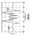
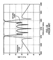
- the order of the channel filter is equivalent to the number of poles in the transfer function and the higher the order the more rejection a channel filter can provide. The number of poles can be seen by looking at a graph of the return loss wherein each peak represents one pole in the transfer function. For each pole there is a physical electrical cavity present in the channel filter. For example, a four-pole filter will have four electrical cavities and a five-pole filter will have five electrical cavities.
- a higher order filter provides greater rejection (i.e. insertion loss) than that of a lower order filter. Accordingly, the use of a high order filter allows for the bandwidth of the channel filter to be expanded since the extra pole(s) provide extra rejection. Overall this results in increased filter bandwidth. At the same time, reasonable filter rejection is maintained. For example, a five-pole filter provides a larger filter bandwidth than that of a four-pole filter because the fifth pole provides extra rejection that allows for the widening of the passband of each channel filter. While the overall filter rejection level associated with the five-pole filter will be reduced due to the widening of the passband, the filter rejection level will still be higher than that of a four-pole filter. In this way, the passband performance is significantly enhanced due to the wider bandwidth and a reasonable level of filter rejection is maintained.
- the four electrical cavities of a four-pole filter will each result in a peak in the filter's return loss.
- the five electrical cavities of a five-pole filter will also each result in a peak in the filter's return loss.
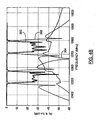
- the five-pole filter will provide more insertion loss (5 POLE IL in FIG. 1C ) (i.e. more rejection) than the four-pole filter (4 POLE IL in FIG. 1C ).
- Microwave multiplexing network filter performance is particularly important in satellite applications since an increase in the insertion loss of the channel filters in the microwave multiplexing network results in a reduction of Effective Isotropic Radiated Power (EIRP) emitted by the satellite and accordingly a reduction in the amount of radio frequency (RF) transmission power that is converted to thermal dissipation. Insertion loss also limits the transmission of spectral regrowth from the power amplifiers that drive the filters.
- EIRP Effective Isotropic Radiated Power
- RF radio frequency
- a method for configuring a microwave multiplexing network including a first channel filter having a top end and a first coupling element, a second channel filter having a top end and a second coupling element, and an interconnect having a top surface and a bottom surface and a short circuit plate, in order to improve channel performance, said method comprising:
- a microwave multiplexing network comprising:
- FIG. 1A is a graph illustrating the return loss and insertion loss characteristics of a prior art four-pole filter
- FIG. 1B is a graph illustrating the return loss and insertion loss characteristics of a prior art five-pole filter
- FIG. 1C is a graph illustrating a comparison of insertion loss characteristics between the four-pole filter of FIG. 1A and the five-pole filter of FIG. 1B ;
- FIG. 2 is a schematic diagram of an exemplary embodiment of a microwave multiplexing network
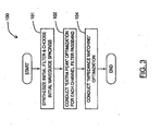
- FIG. 3 is a flowchart of an exemplary embodiment of a method to optimize the design of the microwave multiplexing network of FIG. 2 ;
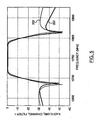
- FIG. 4A is a graph showing the response, in S-parameters, of a dual-channel waveguide manifold coupled multiplexer designed in accordance with a conventional design method
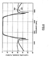
- FIG. 4B is a graph showing the response, in S-parameters, of a dual-channel waveguide manifold coupled multiplexer designed in accordance with the method illustrated in FIG. 3 ;
- FIG. 5 is a graph illustrating a comparison of the first channel filter response of FIG. 4A to that of FIG. 4B ;
- FIG. 6 is a graph illustrating a comparison of the second channel filter response of FIG. 4A to that of FIG. 4B .
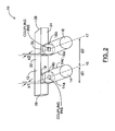
- FIG. 2 is a block diagram that illustrates a microwave multiplexing network 10 in one exemplary embodiment.
- the microwave multiplexing network 10 includes an interconnect 12 (e.g. a microwave waveguide), a first channel filter 14, a second channel filter 16, a first waveguide T-junction 18 and a second waveguide T-junction 20.
- interconnect 12 e.g. a microwave waveguide
- first channel filter 14 e.g. a microwave waveguide
- second channel filter 16 e.g. a first waveguide T-junction 18
- second waveguide T-junction 20 e.g. a microwave waveguide
- FIG. 2 is a block diagram that illustrates a microwave multiplexing network 10 in one exemplary embodiment.
- the microwave multiplexing network 10 includes an interconnect 12 (e.g. a microwave waveguide), a first channel filter 14, a second channel filter 16, a first waveguide T-junction 18 and a second waveguide T-junction 20.
- interconnect 12 e.g. a
- the interconnect 12 has a top wall 22, a bottom wall 24, a short circuit plate 26 and an output end 28.
- the interconnect 12 in one example embodiment is a microwave waveguide 12.
- a waveguide is a device that controls the propagation of an electromagnetic wave so that the electromagnetic wave is forced to follow a particular path and typically takes the form of a hollow metal tube.
- the E-plane of the waveguide is defined as the plane with the largest side and the H-plane as the plane with the small side (E-plane and H-plane not shown in the figures).
- the width and height values of the rectangular manifold waveguide 12 are determined by the frequency of the multiplexer. Usually standard rectangular waveguide sizes are used. For example, the multiplexer having the characteristics shown in FIGS. 4A and 4B or more generally for any multiplexer working within 10.9GHz to 12.7GHz range, the manifold width is usually 0.75" and height is usually 0.375".
- the first and second channel filters 14 and 16 are electromagnetic devices that can be tuned to pass energy that falls within a specific band (i.e. passband) and reject energy that falls outside of that band (i.e. stopband).
- the first and second channel filters 14 and 16 are coupled to the bottom surface 24 or the top surface 22 of the manifold waveguide 12 through the waveguide T-junctions 18 and 20.
- the first and second waveguide T-junctions 18 and 20 are conventional T-junctions.
- the channel filters 14 and 16 are preferably arranged on the manifold waveguide 12 according to centre frequencies such that the highest (or the lowest) frequency channel is adjacent to the shorting plane 26. However, such arrangement is not required.
- the filters 14 and 16 can be doubly terminated or signally terminated filters.
- the first channel filter 14 has a first side wall 14a which is longitudinally spaced from the short circuit plate 26 of the manifold waveguide 12, a top wall 14b, having a first coupling element (e.g. iris) thereon (not shown), that is laterally spaced from the bottom wall 24 of the manifold waveguide 12, and a second side wall 14c.
- the second channel filter 16 has a first side wall 16a which is longitudinally spaced from the second side wall 14c of the first channel filter 14 and from the short circuit plate 26 of the manifold waveguide 12.
- the second channel filter 16 also has a top wall 16b, having a second coupling element (e.g. iris) thereon (not shown), that is laterally spaced from the bottom wall 24 of the manifold waveguide 12.
- microwave multiplexing network 10 could use any coupling element that couples energy between filters and waveguides, such as wire probes.
- the channel filters 14 and 16 are connected parallel to the E-plane of the manifold waveguide 12 to form an E-plane junction.
- the channel filters 14 and 16 could alternatively be connected parallel to the H-plane of the manifold waveguide 12 to form an H-plane junction.
- the input waveguide orientation specifies which plane of a waveguide the filters will be attached to the manifold waveguide, however the enhancement process as described in FIG. 3 will be the same regardless of whether the filters are attached to the H-plane or the E-plane of the manifold waveguide 12.
- the E-plane connection is usually preferred for reasons of compactness since this kind of connection allows for a smaller channel to channel distance to be realized.
- the longitudinal distance d1 is defined by the distance from the short circuit plate 26 of the manifold waveguide 12 to the center 15 of the first coupling iris of the first channel filter 14.
- the longitudinal distance d2 is defined as the distance from the center 15 of the first coupling iris of the first channel filter 14 to the center 17 of the second coupling iris of the second channel filter 16.
- the lateral distance x1 is defined as the distance between the top wall 14b of the first channel filter 14 and the bottom surface 24 of the manifold waveguide 12.
- the lateral distance x2 is defined as the distance from the top wall 16b to the bottom surface 24 of the manifold waveguide 12.
- the channel filters could each be attached to either the top 22 or the bottom 24 surfaces of the manifold waveguide 12.
- the lateral distance x1 is defined as the distance between the top wall 14b of the first channel filter 14 and the top surface 22 of the manifold waveguide 12.
- the lateral distance x2 is defined as the distance from the top wall 16b to the top surface 22 of the manifold waveguide 12.
- short circuit plate 26 discussed above could be replaced with another channel filter, which would be equivalent to making the first interconnect spacing zero.
- FIG. 3 is a flowchart illustrating an example embodiment of a design process 100 for selecting values for the d1, d2, x1 and x2 dimensions for the dual-channel waveguide manifold coupled multiplexer 10 of FIG. 2 such that the overall performance (i.e. bandwidth and filter rejection) of the microwave multiplexing network 10 is enhanced without the addition of any hardware elements.
- the filters 14 and 16 are initially synthesized to approximately meet insertion loss requirements and initial values of waveguide spacings are chosen to correspond to the half-guided wavelength evaluated at the center frequency of the corresponding channel filter.
- the manifold waveguide 12 is considered to be an extra resonator (i.e. electrical cavity) that creates its own real reflection zero within the passband of each of the first and second channel filters 14 and 16.
- This approach is implemented by executing process steps that determine the values of the d1, d2, x1 and x2 dimensions that will produce an extra peak in the passband of each of first and second channel filter 14 and 16.
- the extra peak essentially increases the filter order of the first and second channel filters by one, which in turn results in improved passband flatness and out of band rejection without adding extra hardware.
- step (104) optimization process steps are executed iteratively so that the values for the d1, d2, x1 and x2 dimensions and the internal dimensions of the first and second channel filters 14 and 16 are selected to ensure good impedance matching into the manifold waveguide 12.
- the objective of step (104) is to achieve a return loss with all the passband peaks falling below a certain level, such as -22 dB. Additional details regarding of this step can be found in U.S. Patent No. 4,258,435 .
- the bandwidth of each channel filter can be expanded because the extra pole created by the enhancement process provides extra rejection.
- the additional pole does not actually increase or widen the passband region, but the insertion loss is increased out of band that means that more of the passband can be used without possible interference from one of the other filters.
- the out of band rejection decreases. Therefore, there is a trade-off between bandwidth and out of band rejection. Since the enhancement process 100 provides extra rejection due to the extra passband pole, the filter bandwidth can be expanded while still obtaining better out of band rejection than that which could be obtained by a conventional filter.
- the working frequency was taken to be within 10.9GHz -12.7GHz.
- FIG. 4A is a graph that illustrates the response, using scattering parameters, of a dual-channel waveguide manifold coupled multiplexer designed in accordance with the conventional design process discussed above.
- scattering parameters or S-parameters as they are commonly referred to, form a scattering matrix that describes the response of an n-port network to voltage signals at each port.
- S xy represents the ratio of an output port to an input port and the subscripts, x and y, denote the output and input port numbers respectively.
- S 12 is the ratio of the output port 1 to the input port 2.
- the S-parameter represents the transmission coefficient between those two ports.
- the S-parameter represents the reflection coefficient of that port.
- the graph in FIG. 4A consists of three curves 200, 202 and 204, namely the S 11 curve 200, the S 12 curve 202, and the S 13 curve 204.
- the waveguide output port has been designated port 1
- the first channel filter input port has been designated port 2
- the second channel input port has been designated port 3.
- FIG. 4A shows three scattering parameter curves.
- the S 11 curve 200 is a ratio of the power of the output wave at port 1 to the power of the input wave at port 1 in decibels (dB) as a function of frequency.
- the S 11 curve 200 therefore represents the return loss of the waveguide output port.
- return loss is the ratio in dB of the reflected power of a device to the incident power upon the device.
- the S 12 curve 202 is a ratio of the power of the output wave at port 1 to the power of the input wave at port 2 in dB as a function of frequency.
- S 12 curve 202 represents the insertion loss of the first channel filter.
- insertion loss is the attenuation through a filter.
- the S 13 curve 204 is the ratio of the power of the output wave at port 1 to the power of the input wave at port 3 in dB as a function of frequency. The S 13 curve 204 thus represents the insertion loss of the second channel filter.
- FIG. 4B is a graph that illustrates the response, using scattering parameters, of a dual-channel waveguide manifold coupled multiplexer, this time designed in accordance with the design process 100 discussed above. Specifically, FIG. 4B is a graph showing three curves 300, 302 and 304, namely the S 11 curve 300, the S 12 curve 302, and the S 13 curve 304 that results.
- the S 12 parameters of FIG. 4A and FIG. 4B have been isolated and are comparatively shown in FIG. 5 .
- the S 12 curve 302 is flat over a wider frequency range than the S 12 curve 202, thus the channel filter represented by the S 12 curve 302 has a greater bandwidth than the channel filter represented by the S 12 curve 202. It also can be seen that this increased bandwidth is not achieved at the expense of rejection in the out of band region as it can be seen that the S 12 curve 302 has a much steeper rejection rate than the S 12 curve 202.
- the S 13 parameters of FIG. 4A and FIG. 4B have been isolated and are comparatively shown in FIG. 6 .
- the S 13 curve 304 exhibits wider bandwidth and increased rejection in the out of band region in comparison with those parameters of the S 13 curve 204.
- the two channel filters 14 and 16 did not experience the same level of improvement. This is a common result for the design process 100.
- the overall multiplexer response is improved through use of the design process 100 as noted above, not all channel filters will realize the same performance enhancement. Though generally extra poles (or peaks) can be added into over all multiplexer response for every channel without adding extra cavities, exceptions do exist including not all channel will see the same enhancement, i.e. not all channel filters will have extra poles in their response characteristic.
- the causes can be the overall size constraint, the number of channels, center frequency of each channel and/or bandwidth of each channel. However, in all cases, at least two channel filters will have response characteristics that include additional poles.
- design process 100 can be used to increase the filter order without adding additional hardware, those skilled in the art will appreciate that the design process 100 can be used to achieve the same level of performance with less hardware. For example, traditionally a triple mode filter is achieved through the use of a triple mode cavity, with the design process 100 however, a triple mode filter can be achieved with one less electrical cavity.
Landscapes
- Control Of Motors That Do Not Use Commutators (AREA)
Claims (8)
- Verfahren zum Konfigurieren eines Mikrowellen-Multiplexing-Netzwerks, das einen ersten Kanalfilter (14) mit einem oberen Ende und einem ersten Kopplungselement, einen zweiten Kanalfilter (16) mit einem oberen Ende und einem zweiten Kopplungselement und eine Verbindung (12) mit einer Oberseite (22) und einer Unterseite (24) und einer Kurzschlussplatte (26) aufweist, um die Kanalleistung zu verbessern, wobei das genannte Verfahren die folgenden Schritte beinhaltet:a) Definieren eines ersten Verbindungsabstandswertes (d1) als die Distanz zwischen der Kurzschlussplatte (26) und dem Mittelpunkt (15) des ersten Kopplungselementes und eines zweiten Verbindungsabstandswertes (d2) als die Distanz zwischen dem Mittelpunkt (15) des ersten Kopplungselementes und dem Mittelpunkt (17) des zweiten Kopplungselementes;b) Definieren eines ersten Filter-Verbindung-Abstandswertes (X1) als die Distanz zwischen dem Mittelpunkt (15) des ersten Kopplungselementes und dem Näheren aus Oberseite und Unterseite der Verbindung und Definieren eines zweiten Filter-Verbindung-Abstandswertes (X2) als die Distanz zwischen dem Mittelpunkt (17) des zweiten Kopplungselementes und dem Näheren aus Oberseite und Unterseite der Verbindung;c) Ermitteln des ersten (d1) und des zweiten (d2) Verbindungsabstandswertes und des ersten (X1) und des zweiten (X2) Filter-Verbindung-Abstandswertes durch:für jeden der genannten ersten und zweiten Kanalfilter:i) Auswählen des ersten und des zweiten Verbindungsabstandswertes und des ersten und des zweiten Filter-verbindung-Abstandswertes, um zu gewährleisten, dass eine zusätzliche reale Reflexion von null in das Passband des Mikrowellen-Multiplexing-Netzwerks eingebracht wird und dass die Filterordnung um eins erhöht wird; undd) Koppeln jedes der oberen Enden des ersten und des zweiten Kanalfilters mit dem Näheren aus Oberseite und Unterseite der Verbindung gemäß dem ersten und dem zweiten Verbindungsabstandswert und dem ersten und dem zweiten Filter-Verbindung-Abstandswert.
- Verfahren nach Anspruch 1, wobei c) ferner Folgendes beinhaltet:ii) Auswählen des ersten und des zweiten Verbindungsabstandswertes und des ersten und des zweiten Filter-Verbindung-Abstandswertes, um zu gewährleisten, dass der Rückkehrverlust des Mikrowellen-Multiplexing-Netzwerkes geringer ist als ein vorbestimmter Rückkehrverlustpegel.
- Verfahren nach Anspruch 2, wobei ii) ferner das Justieren der Innenabmessungen des ersten und des zweiten Kanalfilters beinhaltet, um zu gewährleisten, dass der Rückkehrverlust geringer ist als ein vorbestimmter Rückkehrverlustpegel.
- Verfahren nach Anspruch 3, wobei die Verbindung ein Verteilerwellenleiter ist.
- Mikrowellen-Multiplexing-Netzwerk, das Folgendes umfasst:a) einen ersten Kanalfilter (14) mit einem oberen Ende und einem ersten Kopplungselement und einen zweiten Kanalfilter (16) mit einem oberen Ende und einem zweiten Kopplungselement;b) eine Verbindung mit einer Oberseite (22), einer Unterseite (24) und einer Kurzschlussplatte (26);c) wobei der genannte erste Kanalfilter (14) mit einem ersten verbindungsabstandswert (d1), der die Distanz zwischen der Kurzschlussplatte (26) und dem Mittelpunkt (15) des ersten Kopplungselementes repräsentiert, und einem ersten Filter-Verbindung-Abstandswert (X1), der die Distanz zwischen dem Mittelpunkt des ersten Kopplungselementes des ersten Filters und dem Näheren aus Ober- und Unterseite der Verbindung repräsentiert, assoziiert ist;d) wobei der genannte zweite Kanalfilter (16) mit einem zweiten Verbindungsabstandswert (d2), der die Distanz zwischen dem Mittelpunkt (15) des ersten Kopplungselementes und dem Mittelpunkt (17) des zweiten Kopplungselementes repräsentiert, und einem zweiten Filter-Verbindung-Abstandswert (X2), der die Distanz zwischen dem Mittelpunkt des zweiten Kopplungselementes und dem Näheren aus Ober- und Unterseite der Verbindung repräsentiert, assoziiert ist; unde) wobei jedes der genannten oberen Enden des ersten und des zweiten Kanalfilters mit dem Näheren aus Ober- und Unterseite der Verbindung gemäß dem ersten und dem zweiten Verbindungsabstandswert und dem ersten und dem zweiten Filter-Verbindung-Abstandswert gekoppelt ist, wobei der erste und der zweite Verbindungsabstandswert und der erste und der zweite Filter-Verbindung-Abstandswert für jeden der genannten ersten und zweiten Kanalfilter ermittelt werden durch:i) Auswählen des ersten und des zweiten Verbindungsabstandswertes und des ersten und des zweiten Filter-Verbindung-Abstandswertes, um zu gewährleisten, dass eine zusätzliche reale Reflexion von null in das Passband des Mikrowellen-Multiplexing-Netzwerkes eingebracht wird, und wobei die Filterordnung um eins erhöht wird.
- Multiplexing-Netzwerk nach Anspruch 5, wobei e) ferner Folgendes umfasst:ii) Auswählen des ersten und des zweiten Verbindungsabstandswertes und des ersten und des zweiten Filter-Verbindung-Abstandswertes, um zu gewährleisten, dass der Rückkehrverlust des Multiplexing-Netzwerkes geringer ist als ein vorbestimmter Rückkehrverlustpegel.
- Multiplexing-Netzwerk nach Anspruch 6, wobei ii) ferner das Auswählen der Innenabmessungen des ersten und des zweiten Filters beinhaltet, um zu gewährleisten, dass der Rückkehrverlust geringer ist als ein vorbestimmter Rückkehrverlustpegel.
- Multipling-Netzwerk nach Anspruch 6, wobei die Verbindung ein Verteilerwellenleiter ist.
Applications Claiming Priority (1)
| Application Number | Priority Date | Filing Date | Title |
|---|---|---|---|
| US11/350,806 US7397325B2 (en) | 2006-02-10 | 2006-02-10 | Enhanced microwave multiplexing network |
Publications (3)
| Publication Number | Publication Date |
|---|---|
| EP1819010A2 EP1819010A2 (de) | 2007-08-15 |
| EP1819010A3 EP1819010A3 (de) | 2008-04-02 |
| EP1819010B1 true EP1819010B1 (de) | 2009-11-11 |
Family
ID=38137763
Family Applications (1)
| Application Number | Title | Priority Date | Filing Date |
|---|---|---|---|
| EP07250517A Active EP1819010B1 (de) | 2006-02-10 | 2007-02-08 | Erweitertes Mikrowellen-Multiplexing-Netzwerk |
Country Status (3)
| Country | Link |
|---|---|
| US (1) | US7397325B2 (de) |
| EP (1) | EP1819010B1 (de) |
| DE (1) | DE602007003120D1 (de) |
Families Citing this family (2)
| Publication number | Priority date | Publication date | Assignee | Title |
|---|---|---|---|---|
| US7864001B2 (en) * | 2006-04-14 | 2011-01-04 | Spx Corporation | Manifold combiner for multi-station broadcast sites apparatus and method |
| EP2378606A1 (de) * | 2010-04-16 | 2011-10-19 | Astrium Limited | Mehrbandfilter |
Family Cites Families (19)
| Publication number | Priority date | Publication date | Assignee | Title |
|---|---|---|---|---|
| FR1079880A (fr) * | 1953-03-23 | 1954-12-03 | Coupleurs directionnels résonnants | |
| US4029902A (en) * | 1975-10-22 | 1977-06-14 | Hughes Aircraft Company | Contiguous channel multiplexer |
| US4258435A (en) * | 1979-01-08 | 1981-03-24 | Microwave Development Labs. Inc. | Manifold multiplexers |
| US4614920A (en) * | 1984-05-28 | 1986-09-30 | Com Dev Ltd. | Waveguide manifold coupled multiplexer with triple mode filters |
| US4780693A (en) * | 1986-11-12 | 1988-10-25 | Hughes Aircraft Company | Probe coupled waveguide multiplexer |
| US4777459A (en) * | 1987-06-08 | 1988-10-11 | Hughes Aircraft Company | Microwave multiplexer with multimode filter |
| US5233609A (en) * | 1990-08-27 | 1993-08-03 | Gte Government Systems | Multichannel multiplexer with frequency discrimination characteristics |
| US5274344A (en) * | 1991-05-16 | 1993-12-28 | Siemens Aktiengesellschaft | Branch separating filter |
| US5254963A (en) * | 1991-09-25 | 1993-10-19 | Comsat | Microwave filter with a wide spurious-free band-stop response |
| US5235297A (en) * | 1992-03-02 | 1993-08-10 | Saleem Tawil | Directional coupling manifold multiplexer apparatus and method |
| US5428322A (en) * | 1994-02-22 | 1995-06-27 | Hughes Aircraft Company | Microwave waveguide multiplexer |
| GB2313490B (en) * | 1996-05-23 | 2000-09-20 | Matra Marconi Space Uk Ltd | Multiplexing/demultiplexing an FDM or RF signal channels |
| DE19632366A1 (de) * | 1996-08-10 | 1998-02-12 | Bosch Gmbh Robert | Frequenzweiche |
| US6201949B1 (en) * | 1998-05-22 | 2001-03-13 | Rolf Kich | Multiplexer/demultiplexer structures and methods |
| US6191664B1 (en) * | 1999-05-24 | 2001-02-20 | Space Systems/Loral, Inc. | Microwave multiplexer with tunable manifold and method of adjustment |
| US6472951B1 (en) * | 2000-01-05 | 2002-10-29 | Space Systems/Loral, Inc. | Microwave multiplexer with manifold spacing adjustment |
| US6806791B1 (en) * | 2000-02-29 | 2004-10-19 | Radio Frequency Systems, Inc. | Tunable microwave multiplexer |
| JP3688558B2 (ja) * | 2000-06-05 | 2005-08-31 | 三菱電機株式会社 | 導波管群分波器 |
| FR2820884B1 (fr) * | 2001-02-15 | 2003-05-16 | Cit Alcatel | Dispositif d'injection pour unite de filtrage hyperfrequence a resonateurs dielectriques et unite de filtrage incluant un tel dispositif |
-
2006
- 2006-02-10 US US11/350,806 patent/US7397325B2/en active Active
-
2007
- 2007-02-08 DE DE602007003120T patent/DE602007003120D1/de active Active
- 2007-02-08 EP EP07250517A patent/EP1819010B1/de active Active
Also Published As
| Publication number | Publication date |
|---|---|
| DE602007003120D1 (de) | 2009-12-24 |
| US20070188263A1 (en) | 2007-08-16 |
| EP1819010A2 (de) | 2007-08-15 |
| EP1819010A3 (de) | 2008-04-02 |
| US7397325B2 (en) | 2008-07-08 |
Similar Documents
| Publication | Publication Date | Title |
|---|---|---|
| US8860532B2 (en) | Integrated cavity filter/antenna system | |
| KR101010401B1 (ko) | 유전체 모노-블럭 트리플-모드 마이크로웨이브 딜레이 필터 | |
| CN110247190B (zh) | 一种Ku波段波导滤波天线 | |
| CN114069184B (zh) | 一种具有任意功分比的毫米波滤波功分器 | |
| US20070262835A1 (en) | Polarization-preserving waveguide filter and transformer | |
| CN116505219B (zh) | 基于多模折叠基片集成波导的谐振腔、滤波器及设计方法 | |
| CN110336100A (zh) | 一种空气填充siw双通带滤波器及其优化方法 | |
| Kobrin et al. | A novel design of wideband diplexer for base station applications | |
| EP1819010B1 (de) | Erweitertes Mikrowellen-Multiplexing-Netzwerk | |
| Bastioli et al. | An original resonant Y-junction for compact waveguide diplexers | |
| CN108428982A (zh) | 一种腔体三通带滤波器 | |
| CN115332777B (zh) | 一种基片集成波导耦合馈电的低旁瓣滤波天线阵列 | |
| US8008990B2 (en) | Generalized multiplexing network | |
| Doumanis et al. | Transmission zero realization in E-plane filters by means of I/O resonator tapping | |
| Golzar et al. | Orthogonal-mode dual-band rectangular waveguide filters | |
| CN120879181B (zh) | 一种具有反相输出特性的紧凑型w波段滤波功分器 | |
| US12512572B2 (en) | Filters including dual cross-couplings and related combiners | |
| Kobrin et al. | Compact design of diplexer for base stations operating within frequency bands 2.3–2.4/2.49–2.69 GHz | |
| CA3049208C (en) | High-q dispersion-compensated parallel-plate diplexer | |
| Parameswaran et al. | Compact Wide Stop Band Quarter mode SIW Bandpass Filter | |
| CN115313004B (zh) | 一种多入多出腔体输出多工器及设计方法 | |
| KR100763582B1 (ko) | 컴팩트 도파관 필터 | |
| Alibakhshi et al. | Compact and wide stopband E-Plane waveguide diplexer design | |
| Sorkin | Compact Bandpass Waveguide Filters with Capacitive or Mixed Couplings with E-plane Symmetry and without E-plane Symmetry | |
| Tang et al. | Broadband band-stop waveguide filters with T-shape diaphragm |
Legal Events
| Date | Code | Title | Description |
|---|---|---|---|
| PUAI | Public reference made under article 153(3) epc to a published international application that has entered the european phase |
Free format text: ORIGINAL CODE: 0009012 |
|
| AK | Designated contracting states |
Kind code of ref document: A2 Designated state(s): AT BE BG CH CY CZ DE DK EE ES FI FR GB GR HU IE IS IT LI LT LU LV MC NL PL PT RO SE SI SK TR |
|
| AX | Request for extension of the european patent |
Extension state: AL BA HR MK YU |
|
| PUAL | Search report despatched |
Free format text: ORIGINAL CODE: 0009013 |
|
| AK | Designated contracting states |
Kind code of ref document: A3 Designated state(s): AT BE BG CH CY CZ DE DK EE ES FI FR GB GR HU IE IS IT LI LT LU LV MC NL PL PT RO SE SI SK TR |
|
| AX | Request for extension of the european patent |
Extension state: AL BA HR MK YU |
|
| 17P | Request for examination filed |
Effective date: 20081001 |
|
| AKX | Designation fees paid |
Designated state(s): DE ES FR GB IT |
|
| GRAP | Despatch of communication of intention to grant a patent |
Free format text: ORIGINAL CODE: EPIDOSNIGR1 |
|
| GRAS | Grant fee paid |
Free format text: ORIGINAL CODE: EPIDOSNIGR3 |
|
| GRAA | (expected) grant |
Free format text: ORIGINAL CODE: 0009210 |
|
| AK | Designated contracting states |
Kind code of ref document: B1 Designated state(s): DE ES FR GB IT |
|
| REG | Reference to a national code |
Ref country code: GB Ref legal event code: FG4D |
|
| REF | Corresponds to: |
Ref document number: 602007003120 Country of ref document: DE Date of ref document: 20091224 Kind code of ref document: P |
|
| PG25 | Lapsed in a contracting state [announced via postgrant information from national office to epo] |
Ref country code: ES Free format text: LAPSE BECAUSE OF FAILURE TO SUBMIT A TRANSLATION OF THE DESCRIPTION OR TO PAY THE FEE WITHIN THE PRESCRIBED TIME-LIMIT Effective date: 20100222 |
|
| PLBE | No opposition filed within time limit |
Free format text: ORIGINAL CODE: 0009261 |
|
| STAA | Information on the status of an ep patent application or granted ep patent |
Free format text: STATUS: NO OPPOSITION FILED WITHIN TIME LIMIT |
|
| 26N | No opposition filed |
Effective date: 20100812 |
|
| PG25 | Lapsed in a contracting state [announced via postgrant information from national office to epo] |
Ref country code: IT Free format text: LAPSE BECAUSE OF FAILURE TO SUBMIT A TRANSLATION OF THE DESCRIPTION OR TO PAY THE FEE WITHIN THE PRESCRIBED TIME-LIMIT Effective date: 20091111 |
|
| REG | Reference to a national code |
Ref country code: FR Ref legal event code: PLFP Year of fee payment: 10 |
|
| REG | Reference to a national code |
Ref country code: FR Ref legal event code: PLFP Year of fee payment: 11 |
|
| REG | Reference to a national code |
Ref country code: FR Ref legal event code: PLFP Year of fee payment: 12 |
|
| REG | Reference to a national code |
Ref country code: GB Ref legal event code: 732E Free format text: REGISTERED BETWEEN 20181220 AND 20181224 |
|
| REG | Reference to a national code |
Ref country code: DE Ref legal event code: R081 Ref document number: 602007003120 Country of ref document: DE Owner name: HONEYWELL LIMITED HONEYWELL LIMITEE, MISSISSAU, CA Free format text: FORMER OWNER: COM DEV INTERNATIONAL LTD., CAMBRIDGE, ONTARIO, CA Ref country code: DE Ref legal event code: R082 Ref document number: 602007003120 Country of ref document: DE Ref country code: DE Ref legal event code: R081 Ref document number: 602007003120 Country of ref document: DE Owner name: COM DEV LTD., MISSISSAUGA, CA Free format text: FORMER OWNER: COM DEV INTERNATIONAL LTD., CAMBRIDGE, ONTARIO, CA |
|
| REG | Reference to a national code |
Ref country code: GB Ref legal event code: 732E Free format text: REGISTERED BETWEEN 20221020 AND 20221026 |
|
| REG | Reference to a national code |
Ref country code: DE Ref legal event code: R081 Ref document number: 602007003120 Country of ref document: DE Owner name: HONEYWELL LIMITED HONEYWELL LIMITEE, MISSISSAU, CA Free format text: FORMER OWNER: COM DEV LTD., MISSISSAUGA, ONTARIO, CA |
|
| PGFP | Annual fee paid to national office [announced via postgrant information from national office to epo] |
Ref country code: DE Payment date: 20250226 Year of fee payment: 19 |
|
| PGFP | Annual fee paid to national office [announced via postgrant information from national office to epo] |
Ref country code: FR Payment date: 20250224 Year of fee payment: 19 |
|
| PGFP | Annual fee paid to national office [announced via postgrant information from national office to epo] |
Ref country code: GB Payment date: 20250218 Year of fee payment: 19 |