EP1818858A2 - Transponder and method for wireless data transfer - Google Patents
Transponder and method for wireless data transfer Download PDFInfo
- Publication number
- EP1818858A2 EP1818858A2 EP07002809A EP07002809A EP1818858A2 EP 1818858 A2 EP1818858 A2 EP 1818858A2 EP 07002809 A EP07002809 A EP 07002809A EP 07002809 A EP07002809 A EP 07002809A EP 1818858 A2 EP1818858 A2 EP 1818858A2
- Authority
- EP
- European Patent Office
- Prior art keywords
- transponder
- voltage
- base station
- input terminals
- adjustable
- Prior art date
- Legal status (The legal status is an assumption and is not a legal conclusion. Google has not performed a legal analysis and makes no representation as to the accuracy of the status listed.)
- Granted
Links
- 238000000034 method Methods 0.000 title claims abstract description 8
- 230000005540 biological transmission Effects 0.000 claims abstract description 35
- 230000008878 coupling Effects 0.000 claims abstract description 19
- 238000010168 coupling process Methods 0.000 claims abstract description 19
- 238000005859 coupling reaction Methods 0.000 claims abstract description 19
- 230000001939 inductive effect Effects 0.000 claims abstract description 15
- 239000003990 capacitor Substances 0.000 description 6
- 238000001514 detection method Methods 0.000 description 6
- 238000013016 damping Methods 0.000 description 4
- 230000007423 decrease Effects 0.000 description 3
- 238000010586 diagram Methods 0.000 description 3
- 230000000977 initiatory effect Effects 0.000 description 3
- 230000002238 attenuated effect Effects 0.000 description 2
- 230000009467 reduction Effects 0.000 description 2
- 230000008859 change Effects 0.000 description 1
- 230000003111 delayed effect Effects 0.000 description 1
- 230000005672 electromagnetic field Effects 0.000 description 1
- 230000004044 response Effects 0.000 description 1
- 230000001629 suppression Effects 0.000 description 1
Images

Classifications
-
- G—PHYSICS
- G06—COMPUTING; CALCULATING OR COUNTING
- G06K—GRAPHICAL DATA READING; PRESENTATION OF DATA; RECORD CARRIERS; HANDLING RECORD CARRIERS
- G06K19/00—Record carriers for use with machines and with at least a part designed to carry digital markings
- G06K19/06—Record carriers for use with machines and with at least a part designed to carry digital markings characterised by the kind of the digital marking, e.g. shape, nature, code
- G06K19/067—Record carriers with conductive marks, printed circuits or semiconductor circuit elements, e.g. credit or identity cards also with resonating or responding marks without active components
- G06K19/07—Record carriers with conductive marks, printed circuits or semiconductor circuit elements, e.g. credit or identity cards also with resonating or responding marks without active components with integrated circuit chips
- G06K19/0723—Record carriers with conductive marks, printed circuits or semiconductor circuit elements, e.g. credit or identity cards also with resonating or responding marks without active components with integrated circuit chips the record carrier comprising an arrangement for non-contact communication, e.g. wireless communication circuits on transponder cards, non-contact smart cards or RFIDs
Definitions
- the invention relates to a transponder according to the preamble of claim 1 and to a method for wireless data transmission according to the preamble of claim 6.
- RFID Radio Frequency Identification
- the transponders or their transmitting and receiving devices usually do not have an active transmitter for the data transmission to the base station.
- Such inactive systems are referred to as passive systems if they do not have their own power supply, and are referred to as semi-passive systems if they have their own power supply.
- Passive transponders extract the energy needed for their supply from the electromagnetic field emitted by the base station.
- the transponder For data transmission between the transponder and the base station, for example for a programming operation of the transponder, the transponder has an interface of a certain type of interface which is compatible with the corresponding interface type of the base station.
- the interface types can be classified in a first rough outline into contact and contactless types.
- the interface types in which the data transmission takes place contactless or contactless differ, inter alia, by the working or carrier frequency used for data transmission, i. the frequency sent by the base station.
- Commonly used frequencies are for example 125 kHz (LF range), 13.56 MHz (RF range), a frequency range between 860 MHz to 960 MHz (UHF range) and a frequency range greater than 3GHz (microwave range).
- Load modulation For data transmission from a transponder to the base station in the inductive coupling usually the so-called load modulation see, for example, Finkenzeller, chapter 3.2.1.2.1 “Load modulation”.
- the base station For data transmission from the base station to the transponder, the base station in the case of inductive coupling usually transmits a carrier signal with a frequency in a frequency range from 50 kHz to 250 kHz. To initiate the data transmission, the base station first generates a short field gap or so-called "gap" by amplitude modulation of the carrier signal. the amplitude of the carrier signal is briefly attenuated or attenuated or completely suppressed, for example for about 50us to 400us.
- Characters sent by the base station following the initiation of the data transmission are coded by associated time durations between respective temporally successive field gaps.
- a first time value is assigned to a first character value and a second time duration is assigned to at least one second character value.
- the transponder determines the respective time periods between the field gaps and determines the value of the transmitted character from the determined time duration.
- the signal curves generated by the base station and received in the transponder by inductive coupling have specified maximum tolerances, for example with respect to their time profile and / or the level used.
- the quality of a parallel resonant circuit which is formed from the antenna coil and a capacitor connected in parallel thereto, is increased in order to supply the passive ones To enable transponders from the field transmitted by the base station even at greater distances. Due to the reduced damping of the resonant circuit, this causes the coil voltage or the voltage at the parallel resonant circuit of the transponder to decrease more slowly in the case of a field gap than in a resonant circuit with a lower quality and thus higher attenuation.
- the field gap can only be detected in the transponder when the coil voltage or a voltage recovered from the coil voltage by rectification voltage has dropped below an adjustable potential, field gaps are detected delayed compared to a resonant circuit with low quality. As a result, the duration of the field gaps detected in the transponder is shortened and the time intervals between the field gaps are lengthened. This change in the timing of the waveforms detected in the transponder is directly influenced by the quality of the resonant circuit. However, since the timing must be within predetermined limits, the signal transmitted by the base station should have a timing which depends on the quality of the resonant circuit of the transponder, otherwise transmission errors may occur.
- the invention has for its object to provide a transponder and a method for wireless data transmission available that allow a high transmission range between base station and transponder and a substantially Q-independent timing of the signals generated by the base station.
- the invention solves this problem by a transponder according to claim 1 and a method according to claim 6.
- the transponder comprises an input circuit with input terminals for connecting an antenna coil and / or an LC resonant circuit for data transmission with a base station by means of inductive coupling, a first controllable switching means, at least one resistor, which is looped in series with the first controllable switching means between the input terminals of the input circuit, and a control unit which is designed such that it switches through the first switching means, as soon as a voltage present at the input terminals falls below a first adjustable threshold and interrupts again as soon as the voltage at the input terminals is above the first adjustable threshold and / or above a second adjustable threshold for an adjustable period of time.
- the second adjustable threshold is preferably greater than the first adjustable threshold.
- the voltage present at the input terminals can also be rectified to evaluate the signal levels.
- the closed switching means in conjunction with the resistor causes the damping of the resonant circuit in response to a selected resistance increases as soon as a first field gap is detected. After the detection of the first field gap, this leads to a rapid, substantially quality-independent decay of the coil voltage in subsequently generated field gaps.
- the switching means is interrupted, whereby the effective quality of the resonant circuit increases sharply again , whereby a high range is achievable.
- transponder this is passive. Especially with passive transponders can be with the inventive Method to achieve significant range improvements while maintaining the data transmission quality.
- the switching means is a transistor, in particular a MOS transistor.
- the input circuit for the processing of frequencies in a frequency range from 50 kHz to 250 kHz, in particular 125 kHz, is formed.
- the input circuit for the data transmission to the base station comprises a modulation unit with a controllable voltage limiting unit, which is designed such that it limits the voltage applied to the input terminals to a first adjustable maximum value or to a second adjustable maximum value.
- the modulation unit is used in particular for load modulation.
- the voltage limiting unit contains circuit parts which limit or clamp the voltage applied to the input terminals as a function of the control state to the first adjustable maximum value or to the second adjustable maximum value.
- the second maximum value is smaller than the first maximum value and the voltage limiting unit is controlled so that it sets the second, ie smaller, maximum value when the first switching means is turned on, and the first, ie larger, maximum value sets when the first switching means interrupted is. Due to the concomitant simultaneous voltage reduction, when the resistor for damping increase is switched on, the time duration required for the coil voltage to drop again below the first threshold value for detection of the field gap at a field gap is reduced again.
- an ohmic load is connected between the input terminals as soon as a voltage present at the input terminals falls below a first adjustable threshold and turns off again as soon as the voltage at the input terminals is above the first adjustable threshold and / or above a second adjustable threshold for an adjustable period of time.
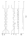
- Fig. 1 shows a passive transponder TR in the form of an integrated circuit with an input circuit EK with input terminals A1 and A2 for connection of an antenna coil L1 for inductive coupling with a conventional base station, not shown.
- the antenna coil L1 is a capacitor C1 connected in parallel, wherein the antenna coil L1 and the capacitor C1 form a parallel resonant circuit whose resonance frequency is tuned to a transmission frequency of the base station of 125kHz.
- the antenna coil L1 forms a transformer coupling with an antenna coil of the base station, not shown.
- the input circuit EK of the transponder TR comprises a controllable voltage limiting unit BE as part of a modulation unit, not shown further, which serves for data transmission from the transponder TR to the base station by means of load modulation.
- a switching element in the form of a MOS transistor T1 and a resistor R1 are connected in series.
- An AC voltage U1 applied to the input terminals A1 and A2 feeds a rectifier GL of the input circuit EK, which generates a supply voltage for the transponder TR.
- the rectified input voltage is supplied to a signal processing unit SV of the input circuit EK for field-gap detection.
- the transponder TR further comprises a control unit SE for controlling the transponder functions, which can be implemented as a microprocessor or as a state machine.
- the control unit SE generates a drive signal WD for the transistor T1, a drive signal MOD for the voltage limiting unit BE and receives a field gap detection signal GAP from the signal processing unit SV.
- Fig. 2 shows timing diagrams in a data transmission from a base station to the transponder of Fig. 1.
- the rectified voltage U1 is again shown as an envelope S1 as an envelope.
- the lower two diagrams show the field gap detection signal GAP and the transistor drive signals WD and MOD, respectively.
- the signals WD and MOD may have identical time courses.
- the base station Before the data transmission, the base station generates by its antenna coil, an alternating magnetic field with a frequency of 125kHz, which induces the AC voltage U1 between the input terminals A1 and A2 due to the inductive coupling.
- An amplitude of the alternating voltage U1 is limited or clamped by the voltage limiting unit BE to a maximum voltage UMAX.
- the base station To initiate the data transmission in the context of a write access to the transponder TR, the base station generates a field gap or a gap by suppression of the carrier signal.
- the voltage U1 of the parallel resonant circuit drops only slowly along the envelope, depending on its quality.
- the course of the rectified voltage U1 is evaluated in the signal processing unit SV.
- the signal processing unit SV When the voltage U1 falls below a threshold value SW for the first time, the signal processing unit SV generates an active signal GAP, i. the control unit SE indicates the detected field gap.
- the control unit SE then activates the signals MOD and WD, i. the transistor T1 is turned on or turned on.
- the through-connected transistor T1 causes an ohmic load in the form of the resistor R1 is connected between the input terminals A1 and A2, whereby the quality of the resonant circuit is reduced or increases its attenuation. This causes the envelope of the voltage U1 to decay significantly faster in the case of a field gap, i. subsequent field gaps can be detected with a much lower delay.
- the signal curve is shown in dashed lines with a lower attenuation, ie without a connected resistor R1.
- a time difference ⁇ t results between the conventional, undamped signal waveform and the more damped waveform of the invention.
- the signal curve according to the invention therefore corresponds much better to an ideal signal curve, in which the voltage U1 or the signal S1 suddenly decreases in the case of a field gap, as a result of which the field gap can be detected without delay.
- the resonant circuit damping is in this case essentially determined by the value of the resistor R1, i. the components caused by the antenna coil L1 and the capacitor C1 are negligible.
- the timing of the signal received by the transponder is therefore independent of the quality of the antenna coil L1 and the capacitor C1 after detection of the first field gap.
- the base station can generate its transmit signal timing independently of which antenna coil type is used in the transponder.
- the voltage limiting unit BE controlled by the active modulation signal MOD causes the voltage U1 to be limited or clamped to a value UWD.
- the voltage reduction of the voltage U1 to the maximum voltage value UWD also causes a faster detectability of a field gap, since the voltage U1 decreases from a lower initial value to the threshold value SW.
- the base station After the initiation of the data transmission by generating the first field gap, the base station switches on its carrier signal again. Due to the activated modulation signal MOD, the voltage limiting unit BE limits the voltage U1 to the value UWD.
- Characters sent by the base station following the initiation of the data transmission are coded by associated time durations t0 and t1, respectively, between time-consecutive field gaps. A first character value "0" is assigned the time duration t0 and a second character value "1" is assigned the time duration t1.
- the transmitted characters of the transponder TR determines the respective Time periods t0 and t1 between the field gaps and determined from the determined time duration, the value of the transmitted character. In the case shown, the exemplary binary string "1010" is transmitted to the transponder.
- the transponder TR recognizes the end of the data transmission. He then deactivates the signals WD and MOD. On the one hand, this causes an increase in the quality of the input resonant circuit and, on the other hand, an increase in the maximum value of the voltage U1 to the value UMAX, since the voltage limiting unit BE limits the voltage U1 to the maximum value UMAX due to the deactivated signal MOD.
- the threshold value SW instead of the threshold value SW, it is also possible to use a further, not shown, for example larger threshold value, in which case it is checked accordingly whether the voltage U1 for the maximum time period tmax is above this threshold value.
- the embodiments shown allow a high transmission range between base station and transponder due to the high usable quality of the input resonant circuits of antenna coil L1 and capacitor C1 and at the same time a substantially Q-independent timing of the signals generated by the base station.
Landscapes
- Engineering & Computer Science (AREA)
- Computer Networks & Wireless Communication (AREA)
- Computer Hardware Design (AREA)
- Microelectronics & Electronic Packaging (AREA)
- Physics & Mathematics (AREA)
- General Physics & Mathematics (AREA)
- Theoretical Computer Science (AREA)
- Near-Field Transmission Systems (AREA)
Abstract
Description
Die Erfindung betrifft einen Transponder nach dem Oberbegriff des Anspruchs 1 sowie ein Verfahren zur drahtlosen Datenübertragung nach dem Oberbegriff des Anspruchs 6.The invention relates to a transponder according to the preamble of claim 1 and to a method for wireless data transmission according to the preamble of claim 6.
Kontaktlose Identifikationssysteme oder so genannte Radio-Frequency-Identification(RFID)-Systeme bestehen üblicherweise aus einer Basisstation bzw. einem Lesegerät oder einer Leseeinheit und einer Vielzahl von Transpondern oder Remote-Sensoren. Die Transponder bzw. deren Sende- und Empfangseinrichtungen verfügen üblicherweise nicht über einen aktiven Sender für die Datenübertragung zur Basisstation. Derartige nicht aktive Systeme werden als passive Systeme bezeichnet, wenn sie keine eigene Energieversorgung aufweisen, und als semipassive Systeme bezeichnet, wenn sie eine eigene Energieversorgung aufweisen. Passive Transponder entnehmen die zu ihrer Versorgung benötigte Energie dem von der Basisstation emittierten elektromagnetischen Feld.Contactless identification systems or so-called Radio Frequency Identification (RFID) systems usually consist of a base station or a reading device or a reading unit and a plurality of transponders or remote sensors. The transponders or their transmitting and receiving devices usually do not have an active transmitter for the data transmission to the base station. Such inactive systems are referred to as passive systems if they do not have their own power supply, and are referred to as semi-passive systems if they have their own power supply. Passive transponders extract the energy needed for their supply from the electromagnetic field emitted by the base station.
Zur Datenübertragung zwischen dem Transponder und der Basisstation, beispielsweise für einen Programmiervorgang des Transponders, weist der Transponder eine Schnittstelle eines bestimmten Schnittstellentyps auf, der kompatibel zum entsprechenden Schnittstellentyp der Basisstation ist. Die Schnittstellentypen können in einer ersten groben Gliederung in kontaktbehaftete und kontaktlose Typen eingeteilt werden.For data transmission between the transponder and the base station, for example for a programming operation of the transponder, the transponder has an interface of a certain type of interface which is compatible with the corresponding interface type of the base station. The interface types can be classified in a first rough outline into contact and contactless types.
Die Schnittstellentypen, bei denen die Datenübertragung kontakt- bzw. berührungslos erfolgt, unterscheiden sich unter anderem durch die zur Datenübertragung verwendete Arbeits- bzw. Trägerfrequenz, d.h. die durch die Basisstation gesendete Frequenz. Häufig verwendete Frequenzen sind beispielsweise 125 kHz (LF-Bereich), 13,56 MHz (RF-Bereich), ein Frequenzbereich zwischen 860 MHz bis 960 MHz (UHF-Bereich) und ein Frequenzbereich größer als 3GHz (Mikrowellenbereich).The interface types in which the data transmission takes place contactless or contactless differ, inter alia, by the working or carrier frequency used for data transmission, i. the frequency sent by the base station. Commonly used frequencies are for example 125 kHz (LF range), 13.56 MHz (RF range), a frequency range between 860 MHz to 960 MHz (UHF range) and a frequency range greater than 3GHz (microwave range).
Ein weiteres Unterscheidungsmerkmal unterschiedlicher Schnittstellentypen ist die Art der Kopplung zwischen den jeweiligen Schnittstellen des Transponders und der Basisstation. Hierbei wird unter anderem zwischen der so genannten induktiven oder magnetischen Kopplung und der so genannten Fernfeldkopplung unterschieden. Vereinfacht dargestellt, bilden bei der induktiven oder Nahfeldkopplung eine Antennenspule der Basisstation und eine an einen Eingangskreis des Transponders angeschlossene Antennenspule einen Transformator, weshalb diese Kopplungsart auch als transformatorische Kopplung bezeichnet wird. Bei der induktiven Kopplung ist eine maximale Entfernung zwischen dem Transponder und der Basisstation auf den Bereich eines Nahfeldes der verwendeten Antennen beschränkt. Der Nahfeldbereich wird im wesentlichen durch die Arbeitsfrequenz der Schnittstelle festgelegt.Another distinguishing feature of different interface types is the nature of the coupling between the respective interfaces of the transponder and the base station. Among other things, a distinction is made between the so-called inductive or magnetic coupling and the so-called far-field coupling. Simplified form, in the inductive or Nahfeldkopplung an antenna coil of the base station and a connected to an input circuit of the transponder antenna coil form a transformer, which is why this type of coupling is also referred to as a transformer coupling. In inductive coupling, a maximum distance between the transponder and the base station is limited to the range of a near field of the antennas used. The near field range is essentially determined by the operating frequency of the interface.
Zur Datenübertragung von einem Transponder zur Basisstation wird bei der induktiven Kopplung in der Regel die so genannte Lastmodulation verwendet, siehe hierzu beispielsweise Finkenzeller, Kapitel 3.2.1.2.1 "Lastmodulation".For data transmission from a transponder to the base station in the inductive coupling usually the so-called load modulation see, for example, Finkenzeller, chapter 3.2.1.2.1 "Load modulation".
Zur Datenübertragung von der Basisstation zum Transponder sendet die Basisstation bei der induktiven Kopplung üblicherweise ein Trägersignal mit einer Frequenz in einem Frequenzbereich von 50kHz bis 250kHz. Zur Einleitung der Datenübertragung erzeugt die Basisstation durch Amplitudenmodulation des Trägersignals zunächst eine kurze Feldlücke oder eine so genannte "Gap", d.h. die Amplitude des Trägersignals wird kurzzeitig, beispielsweise für ca. 50us bis 400us, gedämpft bzw. abgeschwächt oder vollständig unterdrückt.For data transmission from the base station to the transponder, the base station in the case of inductive coupling usually transmits a carrier signal with a frequency in a frequency range from 50 kHz to 250 kHz. To initiate the data transmission, the base station first generates a short field gap or so-called "gap" by amplitude modulation of the carrier signal. the amplitude of the carrier signal is briefly attenuated or attenuated or completely suppressed, for example for about 50us to 400us.
Zeichen, die im Anschluss an die Einleitung der Datenübertragung von der Basisstation gesendet werden, werden durch zugehörige Zeitdauern zwischen jeweils zeitlich aufeinanderfolgenden Feldlücken kodiert. Einem ersten Zeichenwert wird hierbei eine erste Zeitdauer zugeordnet und mindestens einem zweiten Zeichenwert wird eine zweite Zeitdauer zugeordnet. Zur Dekodierung der übertragenen Zeichen ermittelt der Transponder die jeweiligen Zeitdauern zwischen den Feldlücken und bestimmt aus der ermittelten Zeitdauer den Wert des übertragenen Zeichens.Characters sent by the base station following the initiation of the data transmission are coded by associated time durations between respective temporally successive field gaps. In this case, a first time value is assigned to a first character value and a second time duration is assigned to at least one second character value. To decode the transmitted characters, the transponder determines the respective time periods between the field gaps and determines the value of the transmitted character from the determined time duration.
Zur fehlerfreien Datenübertragung bzw. Dekodierung der Zeichen ist es notwendig, dass die von der Basisstation erzeugten und im Transponder durch induktive Kopplung empfangenen Signalverläufe festgelegte, maximale Toleranzen aufweisen, beispielsweise hinsichtlich ihres zeitlichen Verlaufs und/oder der verwendeten Pegel.For error-free data transmission or decoding of the characters, it is necessary that the signal curves generated by the base station and received in the transponder by inductive coupling have specified maximum tolerances, for example with respect to their time profile and / or the level used.
Zur Vergrößerung der erzielbaren Reichweiten zwischen Basisstation und passiven Transpondern wird die Güte eines Parallelschwingkreises, der aus der Antennenspule und einem hierzu parallel geschalteten Kondensator gebildet wird, erhöht, um die Versorgung der passiven Transponder aus dem von der Basisstation gesendeten Feld auch bei größeren Entfernungen zu ermöglichen. Aufgrund der reduzierten Dämpfung des Schwingkreises bewirkt dies, dass bei einer Feldlücke die Spulenspannung bzw. die Spannung am Parallelschwingkreis des Transponders langsamer absinkt als bei einem Schwingkreis mit geringerer Güte und somit höherer Dämpfung. Da die Feldlücke jedoch im Transponder erst erkannt werden kann, wenn die Spulenspannung bzw. eine aus der Spulenspannung durch Gleichrichtung gewonnene Spannung unter ein einstellbares Potential gesunken ist, werden Feldlücken im Vergleich zu einem Schwingkreis mit geringer Güte verzögert erkannt. Dies führt im Ergebnis dazu, dass die Zeitdauer der im Transponder detektierten Feldlücken verkürzt und die Zeitdauern zwischen den Feldlücken verlängert werden. Diese Veränderung des Timings der im Transponder detektierten Signalverläufe wird unmittelbar von der Güte des Schwingkreises beeinflusst. Da das Timing jedoch innerhalb vorbestimmter Grenzwerte liegen muss, sollte das von der Basisstation gesendete Signal ein Timing aufweisen, welches von der Güte des Schwingkreises des Transponders abhängig ist, da sonst Übertragungsfehler entstehen können.To increase the achievable ranges between the base station and passive transponders, the quality of a parallel resonant circuit, which is formed from the antenna coil and a capacitor connected in parallel thereto, is increased in order to supply the passive ones To enable transponders from the field transmitted by the base station even at greater distances. Due to the reduced damping of the resonant circuit, this causes the coil voltage or the voltage at the parallel resonant circuit of the transponder to decrease more slowly in the case of a field gap than in a resonant circuit with a lower quality and thus higher attenuation. However, since the field gap can only be detected in the transponder when the coil voltage or a voltage recovered from the coil voltage by rectification voltage has dropped below an adjustable potential, field gaps are detected delayed compared to a resonant circuit with low quality. As a result, the duration of the field gaps detected in the transponder is shortened and the time intervals between the field gaps are lengthened. This change in the timing of the waveforms detected in the transponder is directly influenced by the quality of the resonant circuit. However, since the timing must be within predetermined limits, the signal transmitted by the base station should have a timing which depends on the quality of the resonant circuit of the transponder, otherwise transmission errors may occur.
Der Erfindung liegt die Aufgabe zugrunde, einen Transponder und ein Verfahren zur drahtlosen Datenübertragung zur Verfügung zu stellen, die eine hohe Übertragungsreichweite zwischen Basisstation und Transponder und ein im wesentlichen güteunabhängiges Timing der von der Basisstation erzeugten Signale ermöglichen.The invention has for its object to provide a transponder and a method for wireless data transmission available that allow a high transmission range between base station and transponder and a substantially Q-independent timing of the signals generated by the base station.
Die Erfindung löst diese Aufgabe durch einen Transponder nach Anspruch 1 sowie ein Verfahren nach Anspruch 6.The invention solves this problem by a transponder according to claim 1 and a method according to claim 6.
Der erfindungsgemäße Transponder umfasst einen Eingangskreis mit Eingangsanschlüssen zum Anschließen einer Antennenspule und/oder eines LC-Schwingkreises zur Datenübertragung mit einer Basisstation mittels induktiver Kopplung, ein erstes ansteuerbares Schaltmittel, mindestens einen Widerstand, der in Serie mit dem ersten ansteuerbaren Schaltmittel zwischen die Eingangsanschlüsse des Eingangskreises eingeschleift ist, und eine Steuereinheit, die derart ausgebildet ist, dass sie das erste Schaltmittel durchschaltet, sobald bzw. wenn eine an den Eingangsanschlüssen anstehende Spannung unter einen ersten einstellbaren Schwellenwert fällt, und wieder unterbricht, sobald bzw. wenn die an den Eingangsanschlüssen anstehende Spannung für eine einstellbare Zeitdauer über dem ersten einstellbaren Schwellenwert und/oder über einem zweiten einstellbaren Schwellenwert liegt. Der zweite einstellbare Schwellenwert ist bevorzugt größer als der erste einstellbare Schwellenwert. Die an den Eingangsanschlüssen anstehende Spannung kann zur Auswertung der Signalpegel auch gleichgerichtet werden. Das geschlossene Schaltmittel in Verbindung mit dem Widerstand bewirkt, dass die Dämpfung des Schwingkreises in Abhängigkeit vom einem gewählten Widerstandswert zunimmt, sobald eine erste Feldlücke detektiert wird. Nach der Detektion der ersten Feldlücke führt dies zu einem raschen, im wesentlichen güteunabhängigen Abklingen der Spulenspannung bei nachfolgend erzeugten Feldlücken. Am Ende der Datenübertragung zwischen der Basisstation und dem Transponder, d.h. sobald die an den Eingangsanschlüssen anstehende Spannung für die einstellbare Zeitdauer über dem ersten und/oder über dem zweiten einstellbaren Schwellenwert liegt, wird das Schaltmittel unterbrochen, wodurch die wirksame Güte des Schwingkreises wieder stark ansteigt, wodurch eine hohe Reichweite erzielbar ist. Insgesamt bedeutet dies, dass trotz hoher Güten des Schwingkreises ein einheitliches Timing der im Transponder empfangenen bzw. der von der Basisstation gesendeten Signale erzielbar ist. Auf diese Weise lassen sich hohe Übertragungsreichweiten und ein güteunabhängiger Betrieb kombinieren.The transponder according to the invention comprises an input circuit with input terminals for connecting an antenna coil and / or an LC resonant circuit for data transmission with a base station by means of inductive coupling, a first controllable switching means, at least one resistor, which is looped in series with the first controllable switching means between the input terminals of the input circuit, and a control unit which is designed such that it switches through the first switching means, as soon as a voltage present at the input terminals falls below a first adjustable threshold and interrupts again as soon as the voltage at the input terminals is above the first adjustable threshold and / or above a second adjustable threshold for an adjustable period of time. The second adjustable threshold is preferably greater than the first adjustable threshold. The voltage present at the input terminals can also be rectified to evaluate the signal levels. The closed switching means in conjunction with the resistor causes the damping of the resonant circuit in response to a selected resistance increases as soon as a first field gap is detected. After the detection of the first field gap, this leads to a rapid, substantially quality-independent decay of the coil voltage in subsequently generated field gaps. At the end of the data transmission between the base station and the transponder, ie as soon as the voltage applied to the input terminals for the adjustable period of time above the first and / or above the second adjustable threshold, the switching means is interrupted, whereby the effective quality of the resonant circuit increases sharply again , whereby a high range is achievable. Overall, this means that, despite high grades of the resonant circuit, a uniform timing of the signals received in the transponder or of the signals transmitted by the base station can be achieved. In this way, high transmission ranges and a quality-independent operation can be combined.
In einer Weiterbildung des Transponders ist dieser passiv. Insbesondere bei passiven Transpondern lassen sich mit dem erfindungsgemäßen Verfahren deutliche Reichweitenverbesserungen bei gleichzeitiger Beibehaltung der Datenübertragungsqualität erzielen.In a further development of the transponder this is passive. Especially with passive transponders can be with the inventive Method to achieve significant range improvements while maintaining the data transmission quality.
In einer Weiterbildung des Transponders ist das Schaltmittel ein Transistor, insbesondere ein MOS-Transistor.In a development of the transponder, the switching means is a transistor, in particular a MOS transistor.
In einer Weiterbildung des Transponders ist der Eingangskreis für die Verarbeitung von Frequenzen in einem Frequenzbereich von 50kHz bis 250kHz, insbesondere 125kHz, ausgebildet.In a further development of the transponder, the input circuit for the processing of frequencies in a frequency range from 50 kHz to 250 kHz, in particular 125 kHz, is formed.
In einer Weiterbildung des Transponders umfasst der Eingangskreis für die Datenübertragung zur Basisstation eine Modulationseinheit mit einer ansteuerbaren Spannungsbegrenzungseinheit, die derart ausgebildet ist, dass sie die an den Eingangsanschlüssen anstehende Spannung auf einen ersten einstellbaren Maximalwert oder auf einen zweiten einstellbaren Maximalwert begrenzt. Die Modulationseinheit dient insbesondere zur Lastmodulation. Die Spannungsbegrenzungseinheit enthält Schaltungsteile, welche die an den Eingangsanschlüssen anstehende Spannung ansteuerungszustandsabhängig auf den ersten einstellbaren Maximalwert oder auf den zweiten einstellbaren Maximalwert begrenzen bzw. klemmen. Bevorzugt ist der zweite Maximalwert kleiner als der erste Maximalwert und die Spannungsbegrenzungseinheit wird derart angesteuert, dass sie den zweiten, d.h. kleineren, Maximalwert einstellt, wenn das erste Schaltmittel durchgeschaltet ist, und den ersten, d.h. größeren, Maximalwert einstellt, wenn das erste Schaltmittel unterbrochen ist. Aufgrund der daraus resultierenden gleichzeitigen Spannungsreduktion, wenn der Widerstand zur Dämpfungserhöhung zugeschaltet wird, wird die Zeitdauer nochmals reduziert, welche die Spulenspannung benötigt, um bei einer Feldlücke unter den ersten Schwellenwert zur Detektion der Feldlücke abzusinken.In one development of the transponder, the input circuit for the data transmission to the base station comprises a modulation unit with a controllable voltage limiting unit, which is designed such that it limits the voltage applied to the input terminals to a first adjustable maximum value or to a second adjustable maximum value. The modulation unit is used in particular for load modulation. The voltage limiting unit contains circuit parts which limit or clamp the voltage applied to the input terminals as a function of the control state to the first adjustable maximum value or to the second adjustable maximum value. Preferably, the second maximum value is smaller than the first maximum value and the voltage limiting unit is controlled so that it sets the second, ie smaller, maximum value when the first switching means is turned on, and the first, ie larger, maximum value sets when the first switching means interrupted is. Due to the concomitant simultaneous voltage reduction, when the resistor for damping increase is switched on, the time duration required for the coil voltage to drop again below the first threshold value for detection of the field gap at a field gap is reduced again.
Bei dem Verfahren zur drahtlosen Datenübertragung mittels induktiver Kopplung zwischen einer Basisstation und einem Transponder, der einen Eingangskreis mit Eingangsanschlüssen zum Anschließen einer Antennenspule und/oder eines LC-Schwingkreises aufweist, wird eine ohmsche Last zwischen den Eingangsanschlüssen zugeschaltet, sobald eine an den Eingangsanschlüssen anstehende Spannung unter einen ersten einstellbaren Schwellenwert fällt, und wieder abgeschaltet, sobald bzw. wenn die an den Eingangsanschlüssen anstehende Spannung für eine einstellbare Zeitdauer über dem ersten einstellbaren Schwellenwert und/oder über einem zweiten einstellbaren Schwellenwert liegt.In the method for wireless data transmission by means of inductive coupling between a base station and a transponder having an input circuit with input terminals for connecting an antenna coil and / or an LC resonant circuit, an ohmic load is connected between the input terminals as soon as a voltage present at the input terminals falls below a first adjustable threshold and turns off again as soon as the voltage at the input terminals is above the first adjustable threshold and / or above a second adjustable threshold for an adjustable period of time.
Die Erfindung wird nachfolgend unter Bezugnahme auf die Zeichnungen beschrieben. Hierbei zeigen schematisch:
- Fig. 1
- einen passiven Transponder mit einem Eingangskreis zum Anschluss einer Antennenspule zur induktiven Kopplung mit einer Basisstation und
- Fig. 2
- Zeitablaufsdiagramme bei einer Datenübertragung von einer Basisstation zu dem Transponder von Fig. 1.
- Fig. 1
- a passive transponder with an input circuit for connecting an antenna coil for inductive coupling with a base station and
- Fig. 2
- Timing diagrams in a data transmission from a base station to the transponder of FIG. 1.
Fig. 1 zeigt einen passiven Transponder TR in Form eines integrierten Schaltkreises mit einem Eingangskreis EK mit Eingangsanschlüssen A1 und A2 zum Anschluss einer Antennenspule L1 zur induktiven Kopplung mit einer nicht gezeigten herkömmlichen Basisstation.Fig. 1 shows a passive transponder TR in the form of an integrated circuit with an input circuit EK with input terminals A1 and A2 for connection of an antenna coil L1 for inductive coupling with a conventional base station, not shown.
Der Antennenspule L1 ist ein Kondensator C1 parallel geschaltet, wobei die Antennenspule L1 und der Kondensator C1 einen Parallelschwingkreis bilden, dessen Resonanzfrequenz auf eine Sendefrequenz der Basisstation von 125kHz abgestimmt ist. Die Antennenspule L1 bildet mit einer nicht gezeigten Antennenspule der Basisstation eine transformatorische Kopplung.The antenna coil L1 is a capacitor C1 connected in parallel, wherein the antenna coil L1 and the capacitor C1 form a parallel resonant circuit whose resonance frequency is tuned to a transmission frequency of the base station of 125kHz. The antenna coil L1 forms a transformer coupling with an antenna coil of the base station, not shown.
Der Eingangskreis EK des Transponders TR umfasst eine ansteuerbare Spannungsbegrenzungseinheit BE als Teil einer nicht weiter gezeigten Modulationseinheit, die zur Datenübertragung vom Transponder TR zur Basisstation mittels Lastmodulation dient.The input circuit EK of the transponder TR comprises a controllable voltage limiting unit BE as part of a modulation unit, not shown further, which serves for data transmission from the transponder TR to the base station by means of load modulation.
Zwischen die Eingangsanschlüsse A1 und A2 des Eingangskreises EK sind ein Schaltelement in Form eines MOS-Transistors T1 und ein Widerstand R1 seriell eingeschleift.Between the input terminals A1 and A2 of the input circuit EK, a switching element in the form of a MOS transistor T1 and a resistor R1 are connected in series.
Eine an den Eingansanschlüssen A1 und A2 anstehende Wechselspannung U1 speist einen Gleichrichter GL des Eingangskreises EK, der eine Versorgungsspannung für den Transponder TR erzeugt. Die gleichgerichtete Eingansspannung wird einer Signalverarbeitungseinheit SV des Eingangskreises EK zur Feldlückendetektion zugeführt.An AC voltage U1 applied to the input terminals A1 and A2 feeds a rectifier GL of the input circuit EK, which generates a supply voltage for the transponder TR. The rectified input voltage is supplied to a signal processing unit SV of the input circuit EK for field-gap detection.
Der Transponder TR umfasst weiterhin eine Steuereinheit SE zur Steuerung der Transponderfunktionen, die als Mikroprozessor oder als Zustandsmaschine realisiert sein kann. Die Steuereinheit SE erzeugt ein Ansteuersignal WD für den Transistor T1, ein Ansteuersignal MOD für die Spannungsbegrenzungseinheit BE und empfängt ein Feldlückendetektionssignal GAP von der Signalverarbeitungseinheit SV.The transponder TR further comprises a control unit SE for controlling the transponder functions, which can be implemented as a microprocessor or as a state machine. The control unit SE generates a drive signal WD for the transistor T1, a drive signal MOD for the voltage limiting unit BE and receives a field gap detection signal GAP from the signal processing unit SV.
Fig. 2 zeigt Zeitablaufsdiagramme bei einer Datenübertragung von einer Basisstation zu dem Transponder von Fig. 1. Von der Spannung U1 ist lediglich die Hüllkurve dargestellt. Die gleichgerichtete Spannung U1 ist als Signal S1 wiederum als Hüllkurve dargestellt. In den unteren beiden Diagrammen sind das Feldlückendetektionssignal GAP bzw. die Transistoransteuersignale WD und MOD dargestellt. Im Falle eines Datenempfangs von der Basisstation können die Signale WD und MOD identische zeitliche Verläufe aufweisen.Fig. 2 shows timing diagrams in a data transmission from a base station to the transponder of Fig. 1. Of the voltage U1, only the envelope is shown. The rectified voltage U1 is again shown as an envelope S1 as an envelope. The lower two diagrams show the field gap detection signal GAP and the transistor drive signals WD and MOD, respectively. In the case of data reception from the base station, the signals WD and MOD may have identical time courses.
Vor der Datenübertragung erzeugt die Basisstation durch ihre Antennenspule ein magnetisches Wechselfeld mit einer Frequenz von 125kHz, welches aufgrund der induktiven Kopplung die Wechselspannung U1 zwischen den Eingangsanschlüssen A1 und A2 induziert. Eine Amplitude der Wechselspannung U1 wird durch die Spannungsbegrenzungseinheit BE auf eine maximale Spannung UMAX begrenzt bzw. geklemmt.Before the data transmission, the base station generates by its antenna coil, an alternating magnetic field with a frequency of 125kHz, which induces the AC voltage U1 between the input terminals A1 and A2 due to the inductive coupling. An amplitude of the alternating voltage U1 is limited or clamped by the voltage limiting unit BE to a maximum voltage UMAX.
Zur Einleitung der Datenübertragung im Rahmen eines schreibenden Zugriffs auf den Transponder TR erzeugt die Basisstation eine Feldlücke bzw. ein Gap durch Unterdrückung des Trägersignals. Die Spannung U1 des Parallelschwingkreises fällt in Abhängigkeit von dessen Güte nur langsam entlang der Hüllkurve ab. Der Verlauf der gleichgerichteten Spannung U1 wird in der Signalverarbeitungseinheit SV ausgewertet. Wenn die Spannung U1 einen Schwellenwert SW erstmalig unterschreitet, erzeugt die Signalverarbeitungseinheit SV ein aktives Signal GAP, d.h. zeigt der Steuereinheit SE die detektierte Feldlücke an.To initiate the data transmission in the context of a write access to the transponder TR, the base station generates a field gap or a gap by suppression of the carrier signal. The voltage U1 of the parallel resonant circuit drops only slowly along the envelope, depending on its quality. The course of the rectified voltage U1 is evaluated in the signal processing unit SV. When the voltage U1 falls below a threshold value SW for the first time, the signal processing unit SV generates an active signal GAP, i. the control unit SE indicates the detected field gap.
Die Steuereinheit SE aktiviert daraufhin die Signale MOD und WD, d.h. der Transistor T1 wird durchgeschaltet bzw. durchgesteuert. Der durchgeschaltete Transistor T1 bewirkt, dass eine ohmsche Last in Form des Widerstands R1 zwischen die Eingangsanschlüssen A1 und A2 zugeschaltet wird, wodurch sich die Güte des Schwingkreises reduziert bzw. dessen Dämpfung erhöht. Dies bewirkt, dass die Hüllkurve der Spannung U1 im Fall einer Feldlücke deutlich schneller abklingt, d.h. nachfolgende Feldlücken sind mit einer deutlich geringeren Verzögerung detektierbar.The control unit SE then activates the signals MOD and WD, i. the transistor T1 is turned on or turned on. The through-connected transistor T1 causes an ohmic load in the form of the resistor R1 is connected between the input terminals A1 and A2, whereby the quality of the resonant circuit is reduced or increases its attenuation. This causes the envelope of the voltage U1 to decay significantly faster in the case of a field gap, i. subsequent field gaps can be detected with a much lower delay.
Dies ist exemplarisch für die zweite Feldlücke gezeigt, wobei der Signalverlauf mit geringerer Dämpfung, d.h. ohne zugeschalteten Widerstand R1, gestrichelt dargestellt ist. Wie aus Fig. 2 ersichtlich ist, ergibt sich bis zur Detektion der Feldlücke eine Zeitdifferenz Δt zwischen dem herkömmlichen, ungedämpften Signalverlauf und dem stärker gedämpften, erfindungsgemäßen Signalverlauf. Der erfindungsgemäße Signalverlauf entspricht daher wesentlich besser einem idealen Signalverlauf, bei dem die Spannung U1 bzw. das Signal S1 bei einer Feldlücke sprungförmig abnimmt, wodurch die Feldlücke unverzögert detektierbar ist.This is shown by way of example for the second field gap, wherein the signal curve is shown in dashed lines with a lower attenuation, ie without a connected resistor R1. As can be seen from FIG. 2, until the field gap is detected, a time difference Δt results between the conventional, undamped signal waveform and the more damped waveform of the invention. The signal curve according to the invention therefore corresponds much better to an ideal signal curve, in which the voltage U1 or the signal S1 suddenly decreases in the case of a field gap, as a result of which the field gap can be detected without delay.
Die Schwingkreisdämpfung wird hierbei im Wesentlichen vom Wert des Widerstands R1 bestimmt, d.h. die durch die Antennenspule L1 und den Kondensator C1 bedingten Anteile sind vernachlässigbar. Das Timing des von dem Transponder empfangenen Signals ist daher nach der Detektion der ersten Feldlücke unabhängig von der Qualität der Antennenspule L1 und des Kondensators C1, d.h. die Basisstation kann ihr Sendesignal timingunabhängig davon erzeugen, welcher Antennenspulentyp im Transponder eingesetzt wird.The resonant circuit damping is in this case essentially determined by the value of the resistor R1, i. the components caused by the antenna coil L1 and the capacitor C1 are negligible. The timing of the signal received by the transponder is therefore independent of the quality of the antenna coil L1 and the capacitor C1 after detection of the first field gap. the base station can generate its transmit signal timing independently of which antenna coil type is used in the transponder.
Die mit dem aktiven Modulationssignal MOD angesteuerte Spannungsbegrenzungseinheit BE bewirkt, dass die Spannung U1 auf einen Wert UWD begrenzt bzw. geklemmt wird. Die Spannungsreduktion der Spannung U1 auf den maximalen Spannungswert UWD bewirkt ebenfalls eine schnellere Detektierbarkeit einer Feldlücke, da die Spannung U1 von einem niedrigeren Anfangswert auf den Schwellenwert SW abnimmt.The voltage limiting unit BE controlled by the active modulation signal MOD causes the voltage U1 to be limited or clamped to a value UWD. The voltage reduction of the voltage U1 to the maximum voltage value UWD also causes a faster detectability of a field gap, since the voltage U1 decreases from a lower initial value to the threshold value SW.
Nach der Einleitung der Datenübertragung durch Erzeugen der ersten Feldlücke schaltet die Basisstation ihr Trägersignal wieder ein. Aufgrund des aktivierten Modulationssignals MOD begrenzt die Spannungsbegrenzungseinheit BE die Spannung U1 auf den Wert UWD. Zeichen, die im Anschluss an die Einleitung der Datenübertragung von der Basisstation gesendet werden, werden durch zugehörige Zeitdauern t0 bzw. t1 zwischen jeweils zeitlich aufeinanderfolgenden Feldlücken kodiert. Einem ersten Zeichenwert "0" wird hierbei die Zeitdauer t0 und einem zweiten Zeichenwert "1" wird die Zeitdauer t1 zugeordnet. Zur Dekodierung der übertragenen Zeichen ermittelt der Transponder TR die jeweiligen Zeitdauern t0 bzw. t1 zwischen den Feldlücken und bestimmt aus der ermittelten Zeitdauer den Wert des übertragenen Zeichens. Im gezeigten Fall wird die exemplarische, binäre Zeichenfolge "1010" an den Transponder übertragen.After the initiation of the data transmission by generating the first field gap, the base station switches on its carrier signal again. Due to the activated modulation signal MOD, the voltage limiting unit BE limits the voltage U1 to the value UWD. Characters sent by the base station following the initiation of the data transmission are coded by associated time durations t0 and t1, respectively, between time-consecutive field gaps. A first character value "0" is assigned the time duration t0 and a second character value "1" is assigned the time duration t1. For decoding the transmitted characters of the transponder TR determines the respective Time periods t0 and t1 between the field gaps and determined from the determined time duration, the value of the transmitted character. In the case shown, the exemplary binary string "1010" is transmitted to the transponder.
Wenn die Basisstation die gewünschte Anzahl von Zeichen übertragen hat, werden nachfolgend keine Feldlücken mehr durch sie erzeugt. Wenn eine maximale Zeitdauer tmax seit der letzten Feldlücke verstrichen ist, d.h. die an den Eingangsanschlüssen A1, A2 anstehende Spannung U1 für die Zeitdauer tmax über dem ersten Schwellenwert SW liegt, erkennt der Transponder TR das Ende der Datenübertragung. Daraufhin deaktiviert er die Signale WD und MOD. Dies bewirkt einerseits eine Güteerhöhung des Eingangsschwingkreises und andererseits eine Erhöhung des maximalen Werts der Spannung U1 auf den Wert UMAX, da die Spannungsbegrenzungseinheit BE aufgrund des deaktivierten Signals MOD die Spannung U1 auf den Maximalwert UMAX begrenzt. Zur Erkennung, ob die Datenübertragung beendet ist, kann anstatt des Schwellenwertes SW auch ein weiter, nicht gezeigter, beispielsweise größerer Schwellenwert verwendet werden, wobei dann entsprechend überprüft wird, ob die Spannung U1 für die maximale Zeitdauer tmax über diesem Schwellenwert liegt.If the base station has transmitted the desired number of characters, subsequently no field gaps are generated by them. When a maximum time tmax has elapsed since the last field gap, i. the voltage U1 present at the input terminals A1, A2 is above the first threshold value SW for the time duration tmax, the transponder TR recognizes the end of the data transmission. He then deactivates the signals WD and MOD. On the one hand, this causes an increase in the quality of the input resonant circuit and, on the other hand, an increase in the maximum value of the voltage U1 to the value UMAX, since the voltage limiting unit BE limits the voltage U1 to the maximum value UMAX due to the deactivated signal MOD. In order to detect whether the data transmission has ended, instead of the threshold value SW, it is also possible to use a further, not shown, for example larger threshold value, in which case it is checked accordingly whether the voltage U1 for the maximum time period tmax is above this threshold value.
Die gezeigten Ausführungsformen ermöglichen eine hohe Übertragungsreichweite zwischen Basisstation und Transponder aufgrund der hohen einsetzbaren Güte der Eingangsschwingkreise aus Antennenspule L1 und Kondensator C1 und gleichzeitig ein im wesentlichen güteunabhängiges Timing der von der Basisstation erzeugten Signale.The embodiments shown allow a high transmission range between base station and transponder due to the high usable quality of the input resonant circuits of antenna coil L1 and capacitor C1 and at the same time a substantially Q-independent timing of the signals generated by the base station.
Claims (6)
gekennzeichnet durch
marked by
dadurch gekennzeichnet, dass
eine ohmsche Last (R1) zwischen den Eingangsanschlüssen (A1, A2) zugeschaltet wird, sobald eine an den Eingangsanschlüssen (A1, A2) anstehende Spannung (U1) unter einen einstellbaren Schwellenwert (SW) fällt, und wieder abgeschaltet wird, sobald die an den Eingangsanschlüssen (A1, A2) anstehende Spannung (U1) für eine einstellbare Zeitdauer (tmax) über dem ersten einstellbaren Schwellenwert (SW) und/oder über einem zweiten einstellbaren Schwellenwert liegt.Method for wireless data transmission by means of inductive coupling between a base station and a transponder (TR) having an input circuit (EK) with input connections (A1, A2) for connecting an antenna coil (L1),
characterized in that
an ohmic load (R1) is connected between the input terminals (A1, A2) as soon as a voltage (U1) present at the input terminals (A1, A2) falls below an adjustable threshold value (SW) and is switched off again as soon as the voltage applied to the Input terminals (A1, A2) voltage (U1) for an adjustable period of time (tmax) above the first adjustable threshold (SW) and / or is above a second adjustable threshold.
Applications Claiming Priority (1)
| Application Number | Priority Date | Filing Date | Title |
|---|---|---|---|
| DE200610007261 DE102006007261A1 (en) | 2006-02-10 | 2006-02-10 | Transponder and method for wireless data transmission |
Publications (3)
| Publication Number | Publication Date |
|---|---|
| EP1818858A2 true EP1818858A2 (en) | 2007-08-15 |
| EP1818858A3 EP1818858A3 (en) | 2008-06-25 |
| EP1818858B1 EP1818858B1 (en) | 2012-12-26 |
Family
ID=38057523
Family Applications (1)
| Application Number | Title | Priority Date | Filing Date |
|---|---|---|---|
| EP20070002809 Active EP1818858B1 (en) | 2006-02-10 | 2007-02-09 | Transponder and method for wireless data transfer |
Country Status (3)
| Country | Link |
|---|---|
| US (2) | US20070194937A1 (en) |
| EP (1) | EP1818858B1 (en) |
| DE (1) | DE102006007261A1 (en) |
Families Citing this family (8)
| Publication number | Priority date | Publication date | Assignee | Title |
|---|---|---|---|---|
| DE502005003571D1 (en) * | 2004-04-19 | 2008-05-15 | Vdo Automotive Ag | Transponder |
| DE102007004814B4 (en) * | 2007-01-31 | 2013-06-06 | Continental Automotive Gmbh | Quality adjustment of a receiving circuit |
| DE102007049486B4 (en) | 2007-10-16 | 2018-08-09 | Texas Instruments Deutschland Gmbh | High performance RFID transponder with fast downlink |
| DE102007049560B4 (en) * | 2007-10-16 | 2013-07-11 | Texas Instruments Deutschland Gmbh | RFID transponder with high downlink data speed |
| DE102010056031B4 (en) * | 2010-12-27 | 2019-10-24 | Atmel Corp. | Passive transponder with a charging circuit and method for generating a supply voltage for a passive transponder |
| CN103842932A (en) * | 2011-09-30 | 2014-06-04 | 英特尔公司 | Maintaining operational stability on a system on a chip |
| US9484629B2 (en) | 2011-11-22 | 2016-11-01 | Microsoft Technology Licensing, Llc | Multi-use antenna |
| CN110086508B (en) * | 2019-03-28 | 2021-08-03 | 惠州Tcl移动通信有限公司 | Voltage adjusting method, system, storage medium and mobile terminal |
Citations (4)
| Publication number | Priority date | Publication date | Assignee | Title |
|---|---|---|---|---|
| EP0732663A2 (en) | 1995-03-15 | 1996-09-18 | Omron Corporation | Data carrier capable of increasing data transmission rate |
| EP0829940A2 (en) | 1996-09-13 | 1998-03-18 | Hitachi, Ltd. | Power transmission system, IC card and information communication system using IC card |
| DE19744782A1 (en) | 1997-10-10 | 1999-04-15 | Anatoli Stobbe | Method of data communications between a read-write device and a transponder |
| WO2002009028A1 (en) | 2000-07-21 | 2002-01-31 | Microcid Sa | Low-power passive transponder |
Family Cites Families (15)
| Publication number | Priority date | Publication date | Assignee | Title |
|---|---|---|---|---|
| US5287112A (en) * | 1993-04-14 | 1994-02-15 | Texas Instruments Incorporated | High speed read/write AVI system |
| US5541604A (en) * | 1993-09-03 | 1996-07-30 | Texas Instruments Deutschland Gmbh | Transponders, Interrogators, systems and methods for elimination of interrogator synchronization requirement |
| GB9408588D0 (en) * | 1994-04-29 | 1994-06-22 | Disys Corp | Passive transponder |
| US6351215B2 (en) * | 1998-06-02 | 2002-02-26 | Rf Code, Inc. | Monitoring antenna system |
| US7180402B2 (en) * | 2000-06-06 | 2007-02-20 | Battelle Memorial Institute K1-53 | Phase modulation in RF tag |
| DE10245747B4 (en) * | 2002-10-01 | 2005-12-01 | Infineon Technologies Ag | Contactless data carrier |
| US7014112B2 (en) * | 2003-04-29 | 2006-03-21 | Hewlett-Packard Development Company, L.P. | Electronic identification label and interrogator for use therewith |
| JP3871667B2 (en) * | 2003-08-18 | 2007-01-24 | 松下電器産業株式会社 | Non-contact IC card |
| US7151455B2 (en) * | 2004-04-30 | 2006-12-19 | Kimberly-Clark Worldwide, Inc. | Activating a data tag by load or orientation or user control |
| DE102004031671B4 (en) * | 2004-06-30 | 2016-01-07 | Infineon Technologies Ag | Modulator circuitry, transceiver, reader and method of forming a modulated signal |
| DE102005032590A1 (en) * | 2004-07-12 | 2006-02-09 | Atmel Germany Gmbh | Modulator for a wireless data transmission device, e.g. for a transponder in an RFID system, has a multistage rectifier circuit and at least a circuit device that is controlled by the modulation control signal in a feedback manner |
| JP4059874B2 (en) * | 2004-09-30 | 2008-03-12 | 富士通株式会社 | Rectifier circuit |
| CA2621920A1 (en) * | 2005-09-23 | 2007-03-29 | Ipico Innovation Inc. | Radio frequency identification device systems |
| WO2008045570A2 (en) * | 2006-10-11 | 2008-04-17 | Kovio, Inc. | Multi-mode tags and methods of making and using the same |
| DE102007049486B4 (en) * | 2007-10-16 | 2018-08-09 | Texas Instruments Deutschland Gmbh | High performance RFID transponder with fast downlink |
-
2006
- 2006-02-10 DE DE200610007261 patent/DE102006007261A1/en not_active Withdrawn
-
2007
- 2007-02-09 EP EP20070002809 patent/EP1818858B1/en active Active
- 2007-02-12 US US11/705,009 patent/US20070194937A1/en not_active Abandoned
-
2011
- 2011-03-01 US US13/037,509 patent/US8847737B2/en active Active
Patent Citations (4)
| Publication number | Priority date | Publication date | Assignee | Title |
|---|---|---|---|---|
| EP0732663A2 (en) | 1995-03-15 | 1996-09-18 | Omron Corporation | Data carrier capable of increasing data transmission rate |
| EP0829940A2 (en) | 1996-09-13 | 1998-03-18 | Hitachi, Ltd. | Power transmission system, IC card and information communication system using IC card |
| DE19744782A1 (en) | 1997-10-10 | 1999-04-15 | Anatoli Stobbe | Method of data communications between a read-write device and a transponder |
| WO2002009028A1 (en) | 2000-07-21 | 2002-01-31 | Microcid Sa | Low-power passive transponder |
Also Published As
| Publication number | Publication date |
|---|---|
| EP1818858A3 (en) | 2008-06-25 |
| US8847737B2 (en) | 2014-09-30 |
| DE102006007261A1 (en) | 2007-08-23 |
| US20110177781A1 (en) | 2011-07-21 |
| EP1818858B1 (en) | 2012-12-26 |
| US20070194937A1 (en) | 2007-08-23 |
Similar Documents
| Publication | Publication Date | Title |
|---|---|---|
| EP1818858B1 (en) | Transponder and method for wireless data transfer | |
| EP0590122B1 (en) | Process and system for transmitting serial data structures for information carrier identification systems, and information carriers | |
| DE69532339T2 (en) | Card readers / writers | |
| DE69831514T2 (en) | identification system | |
| EP1508870B1 (en) | Method for wireless data transmission between a base station and a transponder | |
| EP2256662B1 (en) | Method for detecting identification media | |
| DE10301451A1 (en) | Wireless data transmission method between base station and transponder, by modulating electromagnet waves at receiver using modulation technique based on received field strength | |
| EP0502518A2 (en) | Wireless data transmission method on a data carrier | |
| DE102007034009B4 (en) | A data transmission apparatus and method allowing communication without interference from ambient noise | |
| EP1675033B1 (en) | Wireless data communication method | |
| EP3599573B1 (en) | Method for data transmission between a radio transponder reader and a radio transponder and radio transponder | |
| EP1587023B1 (en) | Method for data communication between a base station and a transponder | |
| DE102006057602B3 (en) | Wireless data transmission method for use in radio frequency identification system, involves assigning time durations to symbol values and selecting data transmission protocol type by describing configuration register in passive transponder | |
| DE102006007262B3 (en) | Wireless transmission data between a base a station and a transponder in a n RFID system uses an inductive path | |
| EP1586917A2 (en) | Method for choosing one or more transponders | |
| EP1836654B1 (en) | Method for locating a backscatterable transponder | |
| DE102008040453B4 (en) | Non-contact communication device and method for contactless communication | |
| EP2141637B1 (en) | Portable data carrier with active contactless interface and operating method | |
| AT401127B (en) | CONTACTLESS DATA TRANSFER SYSTEM | |
| EP2474940B1 (en) | Transponder unit | |
| DE102005009765B3 (en) | Selection of transponder in response area of base station, for use in radio frequency identification applications, transmits arbitration symbol with carrier signal used to allocate time slots | |
| DE19827476C1 (en) | Bidirectional digital data transmission method for use between transponder and read/write device | |
| EP1147487B1 (en) | Method for non-contacting data transmission and transponder for a non-contacting data transmission system | |
| EP1587022B1 (en) | Method for wireless data transfer | |
| DE102004018556A1 (en) | Method for data communication between a base station and a transponder |
Legal Events
| Date | Code | Title | Description |
|---|---|---|---|
| PUAI | Public reference made under article 153(3) epc to a published international application that has entered the european phase |
Free format text: ORIGINAL CODE: 0009012 |
|
| AK | Designated contracting states |
Kind code of ref document: A2 Designated state(s): AT BE BG CH CY CZ DE DK EE ES FI FR GB GR HU IE IS IT LI LT LU LV MC NL PL PT RO SE SI SK TR |
|
| AX | Request for extension of the european patent |
Extension state: AL BA HR MK YU |
|
| RIN1 | Information on inventor provided before grant (corrected) |
Inventor name: KURZ, ALEXANDER Inventor name: BERHORST, MARTIN Inventor name: SCHNEIDER, PETER |
|
| PUAL | Search report despatched |
Free format text: ORIGINAL CODE: 0009013 |
|
| AK | Designated contracting states |
Kind code of ref document: A3 Designated state(s): AT BE BG CH CY CZ DE DK EE ES FI FR GB GR HU IE IS IT LI LT LU LV MC NL PL PT RO SE SI SK TR |
|
| AX | Request for extension of the european patent |
Extension state: AL BA HR MK RS |
|
| 17P | Request for examination filed |
Effective date: 20080715 |
|
| 17Q | First examination report despatched |
Effective date: 20080818 |
|
| AKX | Designation fees paid |
Designated state(s): DE FR |
|
| RAP1 | Party data changed (applicant data changed or rights of an application transferred) |
Owner name: ATMEL AUTOMOTIVE GMBH |
|
| GRAP | Despatch of communication of intention to grant a patent |
Free format text: ORIGINAL CODE: EPIDOSNIGR1 |
|
| GRAS | Grant fee paid |
Free format text: ORIGINAL CODE: EPIDOSNIGR3 |
|
| GRAA | (expected) grant |
Free format text: ORIGINAL CODE: 0009210 |
|
| AK | Designated contracting states |
Kind code of ref document: B1 Designated state(s): DE FR |
|
| REG | Reference to a national code |
Ref country code: DE Ref legal event code: R096 Ref document number: 502007011091 Country of ref document: DE Effective date: 20130307 |
|
| REG | Reference to a national code |
Ref country code: DE Ref legal event code: R082 Ref document number: 502007011091 Country of ref document: DE Representative=s name: GRUENECKER, KINKELDEY, STOCKMAIR & SCHWANHAEUS, DE |
|
| REG | Reference to a national code |
Ref country code: DE Ref legal event code: R081 Ref document number: 502007011091 Country of ref document: DE Owner name: ATMEL CORPORATION, US Free format text: FORMER OWNER: ATMEL GERMANY GMBH, 74072 HEILBRONN, DE Effective date: 20130103 Ref country code: DE Ref legal event code: R082 Ref document number: 502007011091 Country of ref document: DE Representative=s name: GRUENECKER, KINKELDEY, STOCKMAIR & SCHWANHAEUS, DE Effective date: 20130515 Ref country code: DE Ref legal event code: R081 Ref document number: 502007011091 Country of ref document: DE Owner name: ATMEL CORPORATION, US Free format text: FORMER OWNER: ATMEL AUTOMOTIVE GMBH, 74072 HEILBRONN, DE Effective date: 20130515 Ref country code: DE Ref legal event code: R081 Ref document number: 502007011091 Country of ref document: DE Owner name: ATMEL CORPORATION, SAN JOSE, US Free format text: FORMER OWNER: ATMEL GERMANY GMBH, 74072 HEILBRONN, DE Effective date: 20130103 Ref country code: DE Ref legal event code: R081 Ref document number: 502007011091 Country of ref document: DE Owner name: ATMEL CORPORATION, SAN JOSE, US Free format text: FORMER OWNER: ATMEL AUTOMOTIVE GMBH, 74072 HEILBRONN, DE Effective date: 20130515 Ref country code: DE Ref legal event code: R082 Ref document number: 502007011091 Country of ref document: DE Representative=s name: GRUENECKER PATENT- UND RECHTSANWAELTE PARTG MB, DE Effective date: 20130515 |
|
| PLBE | No opposition filed within time limit |
Free format text: ORIGINAL CODE: 0009261 |
|
| STAA | Information on the status of an ep patent application or granted ep patent |
Free format text: STATUS: NO OPPOSITION FILED WITHIN TIME LIMIT |
|
| REG | Reference to a national code |
Ref country code: FR Ref legal event code: ST Effective date: 20131031 |
|
| 26N | No opposition filed |
Effective date: 20130927 |
|
| REG | Reference to a national code |
Ref country code: DE Ref legal event code: R097 Ref document number: 502007011091 Country of ref document: DE Effective date: 20130927 |
|
| PG25 | Lapsed in a contracting state [announced via postgrant information from national office to epo] |
Ref country code: FR Free format text: LAPSE BECAUSE OF NON-PAYMENT OF DUE FEES Effective date: 20130228 |
|
| P01 | Opt-out of the competence of the unified patent court (upc) registered |
Effective date: 20230528 |
|
| PGFP | Annual fee paid to national office [announced via postgrant information from national office to epo] |
Ref country code: DE Payment date: 20240123 Year of fee payment: 18 |