EP1816902A2 - Radiation source for a sensor arrangement with making current limitation - Google Patents
Radiation source for a sensor arrangement with making current limitation Download PDFInfo
- Publication number
- EP1816902A2 EP1816902A2 EP07001061A EP07001061A EP1816902A2 EP 1816902 A2 EP1816902 A2 EP 1816902A2 EP 07001061 A EP07001061 A EP 07001061A EP 07001061 A EP07001061 A EP 07001061A EP 1816902 A2 EP1816902 A2 EP 1816902A2
- Authority
- EP
- European Patent Office
- Prior art keywords
- terminal
- incandescent lamp
- radiation source
- sensor arrangement
- semiconductor switch
- Prior art date
- Legal status (The legal status is an assumption and is not a legal conclusion. Google has not performed a legal analysis and makes no representation as to the accuracy of the status listed.)
- Withdrawn
Links
- 230000005855 radiation Effects 0.000 title claims abstract description 56
- 239000004065 semiconductor Substances 0.000 claims abstract description 28
- 230000003287 optical effect Effects 0.000 claims abstract description 17
- 239000003990 capacitor Substances 0.000 claims abstract description 14
- 238000001228 spectrum Methods 0.000 claims abstract 3
- CURLTUGMZLYLDI-UHFFFAOYSA-N Carbon dioxide Chemical compound O=C=O CURLTUGMZLYLDI-UHFFFAOYSA-N 0.000 claims description 20
- 229910002092 carbon dioxide Inorganic materials 0.000 claims description 15
- 238000005259 measurement Methods 0.000 claims description 15
- 239000012491 analyte Substances 0.000 claims description 5
- 239000001569 carbon dioxide Substances 0.000 claims description 5
- 239000012530 fluid Substances 0.000 claims 1
- 238000004519 manufacturing process Methods 0.000 abstract description 2
- 239000007789 gas Substances 0.000 description 26
- 238000010521 absorption reaction Methods 0.000 description 5
- 230000032683 aging Effects 0.000 description 4
- 238000000034 method Methods 0.000 description 4
- 230000035882 stress Effects 0.000 description 4
- 238000004378 air conditioning Methods 0.000 description 3
- 238000012544 monitoring process Methods 0.000 description 3
- 230000008859 change Effects 0.000 description 2
- 238000004140 cleaning Methods 0.000 description 2
- 238000001514 detection method Methods 0.000 description 2
- 238000010586 diagram Methods 0.000 description 2
- VNWKTOKETHGBQD-UHFFFAOYSA-N methane Chemical compound C VNWKTOKETHGBQD-UHFFFAOYSA-N 0.000 description 2
- 230000008569 process Effects 0.000 description 2
- 206010002091 Anaesthesia Diseases 0.000 description 1
- 238000001949 anaesthesia Methods 0.000 description 1
- 230000037005 anaesthesia Effects 0.000 description 1
- 238000013459 approach Methods 0.000 description 1
- 239000000919 ceramic Substances 0.000 description 1
- 230000001276 controlling effect Effects 0.000 description 1
- 239000002826 coolant Substances 0.000 description 1
- 230000007547 defect Effects 0.000 description 1
- 230000001419 dependent effect Effects 0.000 description 1
- 230000006012 detection of carbon dioxide Effects 0.000 description 1
- 238000011161 development Methods 0.000 description 1
- 230000018109 developmental process Effects 0.000 description 1
- 239000007792 gaseous phase Substances 0.000 description 1
- 238000010438 heat treatment Methods 0.000 description 1
- 239000007788 liquid Substances 0.000 description 1
- 239000007791 liquid phase Substances 0.000 description 1
- 230000007774 longterm Effects 0.000 description 1
- 239000012071 phase Substances 0.000 description 1
- 230000009467 reduction Effects 0.000 description 1
- 230000001105 regulatory effect Effects 0.000 description 1
- 230000000630 rising effect Effects 0.000 description 1
Images


Classifications
-
- H—ELECTRICITY
- H05—ELECTRIC TECHNIQUES NOT OTHERWISE PROVIDED FOR
- H05B—ELECTRIC HEATING; ELECTRIC LIGHT SOURCES NOT OTHERWISE PROVIDED FOR; CIRCUIT ARRANGEMENTS FOR ELECTRIC LIGHT SOURCES, IN GENERAL
- H05B39/00—Circuit arrangements or apparatus for operating incandescent light sources
- H05B39/02—Switching on, e.g. with predetermined rate of increase of lighting current
-
- G—PHYSICS
- G01—MEASURING; TESTING
- G01J—MEASUREMENT OF INTENSITY, VELOCITY, SPECTRAL CONTENT, POLARISATION, PHASE OR PULSE CHARACTERISTICS OF INFRARED, VISIBLE OR ULTRAVIOLET LIGHT; COLORIMETRY; RADIATION PYROMETRY
- G01J3/00—Spectrometry; Spectrophotometry; Monochromators; Measuring colours
- G01J3/02—Details
- G01J3/10—Arrangements of light sources specially adapted for spectrometry or colorimetry
- G01J3/108—Arrangements of light sources specially adapted for spectrometry or colorimetry for measurement in the infrared range
-
- G—PHYSICS
- G01—MEASURING; TESTING
- G01N—INVESTIGATING OR ANALYSING MATERIALS BY DETERMINING THEIR CHEMICAL OR PHYSICAL PROPERTIES
- G01N21/00—Investigating or analysing materials by the use of optical means, i.e. using sub-millimetre waves, infrared, visible or ultraviolet light
- G01N21/17—Systems in which incident light is modified in accordance with the properties of the material investigated
- G01N21/25—Colour; Spectral properties, i.e. comparison of effect of material on the light at two or more different wavelengths or wavelength bands
- G01N21/31—Investigating relative effect of material at wavelengths characteristic of specific elements or molecules, e.g. atomic absorption spectrometry
- G01N21/35—Investigating relative effect of material at wavelengths characteristic of specific elements or molecules, e.g. atomic absorption spectrometry using infrared light
-
- G—PHYSICS
- G01—MEASURING; TESTING
- G01N—INVESTIGATING OR ANALYSING MATERIALS BY DETERMINING THEIR CHEMICAL OR PHYSICAL PROPERTIES
- G01N21/00—Investigating or analysing materials by the use of optical means, i.e. using sub-millimetre waves, infrared, visible or ultraviolet light
- G01N21/17—Systems in which incident light is modified in accordance with the properties of the material investigated
- G01N21/25—Colour; Spectral properties, i.e. comparison of effect of material on the light at two or more different wavelengths or wavelength bands
- G01N21/31—Investigating relative effect of material at wavelengths characteristic of specific elements or molecules, e.g. atomic absorption spectrometry
- G01N21/35—Investigating relative effect of material at wavelengths characteristic of specific elements or molecules, e.g. atomic absorption spectrometry using infrared light
- G01N21/3504—Investigating relative effect of material at wavelengths characteristic of specific elements or molecules, e.g. atomic absorption spectrometry using infrared light for analysing gases, e.g. multi-gas analysis
Definitions
- This invention relates to a radiation source for an optical sensor arrangement and to a corresponding optical sensor arrangement.
- this invention relates to gas sensor arrangements which can be used in optical gas sensors, for example to detect CO 2 .
- optical sensor arrangements are based on the principle that the radiation which is emitted by a radiation source passes through a measured distance, in which the analyte to be detected is present, and the change which occurs in the radiation intensity because of the presence of the analyte is evaluated by means of a corresponding detector.
- the radiation intensity can be affected by absorption, scattering or turbidity, and the analyte can be present in the liquid or gaseous phase.
- Known gas sensor arrangements are used to detect the most diverse analytes, such as methane or carbon dioxide. They are based on the property of many polyatomic gases, that they absorb radiation, particularly in the infrared wavelength range. This absorption occurs at a wavelength which is characteristic of the relevant gas, for example for CO 2 at 4.24 ⁇ m. Using infrared gas sensors, it is therefore possible to establish the presence of a gas component and/or the concentration of this gas component in a gas to be measured.
- Known gas sensor arrangements such as are disclosed, for instance, in DE 10 2004 028077 A1 or DE 10 2004 007 946 A1 , have a radiation source, an absorption distance, i.e. a measurement space, and a radiation detector.
- the radiation intensity which the radiation detector measures is a measurement of the concentration of the absorbing gas.
- NDIR non dispersive infrared
- a broadband radiation source is used, and the relevant wavelength can be set via an interference filter or grating.
- Carbon dioxide detection in particular is gaining increasing significance today in many application areas.
- the quality of the internal air can be monitored, the cleaning cycle of self-cleaning ovens can be monitored, and the supply of CO 2 to plants in greenhouses can be regulated.
- the air of a patient's breath can be monitored, and finally, wherever the danger of escaping CO 2 exists, for instance in correspondingly filled air-conditioning systems, a carbon dioxide sensor can be used in a warning system.
- carbon dioxide detection can be used to increase the energy efficiency of heating and air-conditioning, to monitor the CO 2 content of the interior air, to cause a fresh air supply by controlling an appropriate fan flap only if necessary, i.e. in the case of increased CO 2 concentration.
- CO 2 gas sensors can also fulfil a monitoring function in the motor vehicle field in relation to escaping CO 2 in the case of any defects.
- gas sensor arrangements must meet the highest requirements for robustness, reliability, miniaturisability, but also resistance to aging.
- the radiation source is not usually operated uniformly, but pulsed at a specified frequency, i.e. the radiation source, which is usually in the form of a miniature incandescent lamp which is operated by direct current, is switched on briefly by rectangular pulses.
- Such a known radiation source is shown schematically in Fig. 1.
- Fig. 1 Such a known radiation source is shown schematically in Fig. 1.
- Fig. 3 In which the lamp current upon switching on is shown depending on time, as curve 301.
- the object on which this invention is based is therefore to reduce the stress of a radiation source formed through an incandescent lamp for an optical sensor arrangement in pulsed operation, and thus to increase the lifetime, without excessively increasing the size and production costs.
- This invention is based on the idea that in an optical sensor arrangement, for example a gas sensor arrangement, the incandescent lamp which emits the radiation to be detected is switched on electronically, and the very rapid change of the semiconductor resistance from high to low is avoided by connecting it to a capacitor.
- This capacitor which is provided between a control terminal of the semiconductor switch and the first terminal (which is connected to the lamp) of the semiconductor switch, slows down the switching performance of the semiconductor, which therefore switches through more slowly and thus reduces the making current which flows through the lamp and could affect its long-term stability.
- the lifetime of lamps which are used as a radiation source in a gas sensor is considerably extended, particularly in the case of applications with pulsing lamp operation. Additionally, the peak current consumption of the application can be notably reduced, for which reason smaller components also can be used in some circumstances.
- the peak currents which occur are no longer effective as sources of interference. This is particularly important in the motor vehicle field, for smooth running of electronic control processes.
- control terminal can be connected via a first resistor to the control signal, and also via a second resistor to the reference potential.
- this second resistor can also be replaced by a capacitor.
- the solution according to the invention provides especially efficient reduction of the peak currents which occur if the semiconductor switch is a MOSFET, the first terminal being a drain terminal, the second terminal being a source terminal, and the control terminal being a gate terminal of the MOSFET.
- an n-channel enhancement FET could be used here.
- the so-called Miller capacitance which is present in any case between the gate and the drain, and which the component manufacturers usually keep as low as possible to speed up the switching performance, is amplified by the external circuit, and the switching performance of the MOSFET is thus slowed down directly, to keep the peak currents which occur at switching on as low as possible.
- the arrangement can be used most effectively if a direct current (DC) voltage supply is used.
- the reference potential can be an ground potential.
- the circuit according to the invention can be used especially advantageously with a miniature incandescent lamp with a maximum power consumption of 0.5 W to 5.0 W. Higher powers are possible in principle, but they necessitate actions to avoid damage by the power losses which occur.
- the radiation source according to the invention can be used especially advantageously in optical sensor arrangements, in which the control signal is a pulsed signal, to operate the incandescent lamp in such a way that it emits light pulses which are defined by the control signal, because precisely in the case of such sensor arrangements, the stress due to possibly occurring peak making currents is especially damaging.
- optical sensor arrangement according to the invention can be used, in particular, for detection of carbon dioxide, for example in the motor vehicle field, both for monitoring CO 2 escaping from leaks and for checking the air quality in the passenger internal space.
- the sensor arrangement according to the invention can also be used to detect other gases, to measure turbidity or similarly in liquids.
- the basic idea of this invention can also be transferred to the field of use of a sensor arrangement in which a measurement radiation source and a reference radiation source are compared with each other during a referencing phase.
- the lifetime of both the measurement radiation source and the reference radiation source can be advantageously increased.
- An example of such an arrangement is known from German patent specification DE 199 25 196 C2 .
- the reference radiation source is not used for normal measurement, but is operated at large monitoring intervals to determine the aging of the measurement radiation source. This operation of the reference radiation source at large time intervals and for only short duration is necessary here so that the aging of the reference radiation source can be neglected compared with the aging of the measurement radiation source.
- a miniature incandescent lamp 101 is used as the infrared source.
- This incandescent lamp 101 is connected by a first terminal to a supply voltage V S , in the shown application case of a DC voltage, and by its second terminal, via a semiconductor switch V1, here an n-channel enhancement MOSFET, to ground.
- the semiconductor switch V1 is switched on and off at its gate terminal G by a pulsed control signal V CONTROL .
- the incandescent lamp 101 can be controlled by switching the semiconductor switch V1 on and off so that it emits light pulses.
- the radiation source 102 forms the infrared source of a gas sensor unit 100, as shown in Fig. 4.
- the principles according to the invention can be used in the general sensor field, with all optical methods in which the turbidity or absorption is measured.
- the measurement gas 110 is pumped or diffused into the gas measurement space 104, through the inlets and outlets 112, 114.
- the gas concentration can be determined electro-optically via the absorption of a particular wavelength in the infrared range.
- the emitted infrared radiation 116 is guided through the gas measurement space 104 to the detector 108.
- the detector 108 has an optical wavelength filter 106, which lets through only the wavelength range in which the gas molecules to be detected absorb. Other gas molecules normally absorb no light at this wavelength, and therefore do not affect the amount of radiation which reaches the detector 108.
- the IR signal is pulsed by the radiation source 102 by driving the semiconductor switch V1 appropriately, to be able to filter thermal background signals out of the desired signal.
- a controller 120 drives the radiation source 102 on the one hand, and on the other hand receives the output signals of the detector 108 and processes them further.
- a temperature sensor 124 can also be provided, to capture the temperature in the gas measurement space 104.
- the circuit according to the invention of the semiconductor switch V1 which in this case is a MOSFET and includes a capacitor C2, is connected by one terminal to the drain terminal of the MOSFET, and by its second terminal to the gate terminal of the MOSFET.
- a first resistor R1 is connected on the one hand to the control terminal of the MOSFET and on the other hand to the control signal V CONTROL to control the lamp.
- a second resistor R2 is provided between the gate terminal of the MOSFET and ground.
- the second resistor R2 can be replaced by a capacitor (not shown here).
- Fig. 3 shows the lamp current I L through the incandescent lamp 101 over time when the semiconductor switch V1 is switched on, i.e. when a rising pulse occurs on the control signal V CONTROL .
- the curve 302 shows lamp current in the circuit according to Fig. 2, in comparison with a current curve 301 when the semiconductor switch is connected according to the arrangement of Fig. 1.
- the incandescent lamp 101 is, for instance, a miniature incandescent lamp which is operated at around 6 V and at very low power ranges
- the components R1, R2 and C2 can be implemented as thick film resistors according to industry standard format 0603, or the capacitor can be implemented as a ceramic multi-layer chip capacitor according to industry standard format 0603 or 0805. In this way, the whole circuit can be miniaturised to a very large extent.
- the semiconductor switch V1 can be provided as a SOT 23, for instance.
Landscapes
- Physics & Mathematics (AREA)
- Spectroscopy & Molecular Physics (AREA)
- General Physics & Mathematics (AREA)
- Health & Medical Sciences (AREA)
- Life Sciences & Earth Sciences (AREA)
- Chemical & Material Sciences (AREA)
- Analytical Chemistry (AREA)
- Biochemistry (AREA)
- General Health & Medical Sciences (AREA)
- Immunology (AREA)
- Pathology (AREA)
- Investigating Or Analysing Materials By Optical Means (AREA)
- Circuit Arrangement For Electric Light Sources In General (AREA)
Abstract
Description
- This invention relates to a radiation source for an optical sensor arrangement and to a corresponding optical sensor arrangement. In particular, this invention relates to gas sensor arrangements which can be used in optical gas sensors, for example to detect CO2.
- In general, optical sensor arrangements are based on the principle that the radiation which is emitted by a radiation source passes through a measured distance, in which the analyte to be detected is present, and the change which occurs in the radiation intensity because of the presence of the analyte is evaluated by means of a corresponding detector. The radiation intensity can be affected by absorption, scattering or turbidity, and the analyte can be present in the liquid or gaseous phase.
- Known gas sensor arrangements are used to detect the most diverse analytes, such as methane or carbon dioxide. They are based on the property of many polyatomic gases, that they absorb radiation, particularly in the infrared wavelength range. This absorption occurs at a wavelength which is characteristic of the relevant gas, for example for CO2 at 4.24 µm. Using infrared gas sensors, it is therefore possible to establish the presence of a gas component and/or the concentration of this gas component in a gas to be measured.
- Known gas sensor arrangements, such as are disclosed, for instance, in
DE 10 2004 028077 A1 orDE 10 2004 007 946 A1 , have a radiation source, an absorption distance, i.e. a measurement space, and a radiation detector. According to the known Lambert-Beer law, the radiation intensity which the radiation detector measures is a measurement of the concentration of the absorbing gas. In the case of these so-called NDIR (non dispersive infrared) sensors, a broadband radiation source is used, and the relevant wavelength can be set via an interference filter or grating. - Carbon dioxide detection in particular is gaining increasing significance today in many application areas. For instance, the quality of the internal air can be monitored, the cleaning cycle of self-cleaning ovens can be monitored, and the supply of CO2 to plants in greenhouses can be regulated. In the medical field, for example in anaesthesia, the air of a patient's breath can be monitored, and finally, wherever the danger of escaping CO2 exists, for instance in correspondingly filled air-conditioning systems, a carbon dioxide sensor can be used in a warning system.
- In the motor vehicle field, carbon dioxide detection can be used to increase the energy efficiency of heating and air-conditioning, to monitor the CO2 content of the interior air, to cause a fresh air supply by controlling an appropriate fan flap only if necessary, i.e. in the case of increased CO2 concentration.
- Also, modern motor vehicle air-conditioning systems are based on CO2 as the coolant, so that CO2 gas sensors can also fulfil a monitoring function in the motor vehicle field in relation to escaping CO2 in the case of any defects. Particularly in the motor vehicle field, such gas sensor arrangements must meet the highest requirements for robustness, reliability, miniaturisability, but also resistance to aging.
- In the case of known gas sensor arrangements, such as arrangements which are disclosed in
DE 10 2004 028 077 A1 , the radiation source is not usually operated uniformly, but pulsed at a specified frequency, i.e. the radiation source, which is usually in the form of a miniature incandescent lamp which is operated by direct current, is switched on briefly by rectangular pulses. - It has been shown that the lamps which are switched on and off again and again are exposed to increased stress because of the making current which occurs each time, and thus have a shorter lifetime. To extend the lifetime of such incandescent lamps, which are switched on in pulsed operation, and in particular to reduce the high making current peaks, a known method is to switch the lamp on by a semiconductor, and to provide an RC element in the control circuit, to make it possible to switch the lamp on smoothly.
- Such a known radiation source is shown schematically in Fig. 1. However, at the time of switching on there is always an overcurrent at a multiple, usually five to ten times, of the nominal current. This is shown in Fig. 3, in which the lamp current upon switching on is shown depending on time, as
curve 301. - The cause of this high peak current can be seen in that the incandescent lamp filament in the cold state of the lamp has a significantly lower electrical resistance than in the hot operating state. It is only after a few milliseconds of operation that the incandescent filament reaches its operating temperature and thus its final electrical resistance, and the current through the lamp approaches the operating current value.
- The object on which this invention is based is therefore to reduce the stress of a radiation source formed through an incandescent lamp for an optical sensor arrangement in pulsed operation, and thus to increase the lifetime, without excessively increasing the size and production costs.
- This object is achieved by a radiation source with the features of claim 1. This object is also achieved by an optical sensor arrangement with the features of claim 6. Advantageous developments of this invention are the subject of the dependent claims.
- This invention is based on the idea that in an optical sensor arrangement, for example a gas sensor arrangement, the incandescent lamp which emits the radiation to be detected is switched on electronically, and the very rapid change of the semiconductor resistance from high to low is avoided by connecting it to a capacitor. This capacitor, which is provided between a control terminal of the semiconductor switch and the first terminal (which is connected to the lamp) of the semiconductor switch, slows down the switching performance of the semiconductor, which therefore switches through more slowly and thus reduces the making current which flows through the lamp and could affect its long-term stability.
- Advantageously, by the solution according to the invention, the lifetime of lamps which are used as a radiation source in a gas sensor is considerably extended, particularly in the case of applications with pulsing lamp operation. Additionally, the peak current consumption of the application can be notably reduced, for which reason smaller components also can be used in some circumstances.
- Advantageously, the peak currents which occur are no longer effective as sources of interference. This is particularly important in the motor vehicle field, for smooth running of electronic control processes.
- According to the invention, the control terminal can be connected via a first resistor to the control signal, and also via a second resistor to the reference potential. Alternatively, this second resistor can also be replaced by a capacitor.
- The solution according to the invention provides especially efficient reduction of the peak currents which occur if the semiconductor switch is a MOSFET, the first terminal being a drain terminal, the second terminal being a source terminal, and the control terminal being a gate terminal of the MOSFET. For instance, an n-channel enhancement FET could be used here. In the case of a MOSFET as the semiconductor switch, the so-called Miller capacitance which is present in any case between the gate and the drain, and which the component manufacturers usually keep as low as possible to speed up the switching performance, is amplified by the external circuit, and the switching performance of the MOSFET is thus slowed down directly, to keep the peak currents which occur at switching on as low as possible.
- Because the switching performance of the semiconductor switch is slowed down by the circuit according to the invention, the arrangement can be used most effectively if a direct current (DC) voltage supply is used. In this case, the reference potential can be an ground potential.
- Also, since energy is converted into power loss by the recharging of the capacitance between the control terminal and the first terminal and also by the resistor circuit, the circuit according to the invention can be used especially advantageously with a miniature incandescent lamp with a maximum power consumption of 0.5 W to 5.0 W. Higher powers are possible in principle, but they necessitate actions to avoid damage by the power losses which occur.
- The radiation source according to the invention can be used especially advantageously in optical sensor arrangements, in which the control signal is a pulsed signal, to operate the incandescent lamp in such a way that it emits light pulses which are defined by the control signal, because precisely in the case of such sensor arrangements, the stress due to possibly occurring peak making currents is especially damaging.
- The advantageous properties of the optical sensor arrangement according to the invention can be used, in particular, for detection of carbon dioxide, for example in the motor vehicle field, both for monitoring CO2 escaping from leaks and for checking the air quality in the passenger internal space. Obviously, however, the sensor arrangement according to the invention can also be used to detect other gases, to measure turbidity or similarly in liquids.
- The basic idea of this invention can also be transferred to the field of use of a sensor arrangement in which a measurement radiation source and a reference radiation source are compared with each other during a referencing phase. In this application case, the lifetime of both the measurement radiation source and the reference radiation source can be advantageously increased. An example of such an arrangement is known from
German patent specification DE 199 25 196 C2 . The reference radiation source is not used for normal measurement, but is operated at large monitoring intervals to determine the aging of the measurement radiation source. This operation of the reference radiation source at large time intervals and for only short duration is necessary here so that the aging of the reference radiation source can be neglected compared with the aging of the measurement radiation source. - On the basis of the advantageous versions which are shown in the attached drawings, the invention is explained in more detail below.
- Similar or corresponding details of the subject matter of the invention are given the same reference symbols. In the drawings:
- Fig. 1 shows a radiation source with RC circuit according to the prior art;
- Fig. 2 shows a radiation source with a circuit according to the invention to reduce the peak current;
- Fig. 3 is a time representation of the making currents through the incandescent lamp for the circuits according to Figs. 1 and 2;
- Fig. 4 is a block diagram of an optical sensor arrangement according to the invention and a first embodiment;
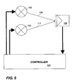
- Fig. 5 is a block diagram of an optical sensor arrangement according to the invention and another embodiment.
- As shown in Fig. 2, for a
radiation source 102 according to the invention, for use in a so-called NDIR (non dispersive infrared) sensor, a miniatureincandescent lamp 101 is used as the infrared source. Thisincandescent lamp 101 is connected by a first terminal to a supply voltage VS, in the shown application case of a DC voltage, and by its second terminal, via a semiconductor switch V1, here an n-channel enhancement MOSFET, to ground. The semiconductor switch V1 is switched on and off at its gate terminal G by a pulsed control signal VCONTROL. - A single pulse, for which the HIGH level corresponds to a switched-on state of the lamp, is shown schematically at the input. In this way, the
incandescent lamp 101 can be controlled by switching the semiconductor switch V1 on and off so that it emits light pulses. - The
radiation source 102 according to the invention forms the infrared source of agas sensor unit 100, as shown in Fig. 4. The basic components here, apart from theinfrared source 102, are thegas measurement space 104, awavelength filter 106 and aninfrared detector 108. However, the principles according to the invention can be used in the general sensor field, with all optical methods in which the turbidity or absorption is measured. - The
measurement gas 110 is pumped or diffused into thegas measurement space 104, through the inlets andoutlets infrared radiation 116 is guided through thegas measurement space 104 to thedetector 108. Thedetector 108 has anoptical wavelength filter 106, which lets through only the wavelength range in which the gas molecules to be detected absorb. Other gas molecules normally absorb no light at this wavelength, and therefore do not affect the amount of radiation which reaches thedetector 108. The IR signal is pulsed by theradiation source 102 by driving the semiconductor switch V1 appropriately, to be able to filter thermal background signals out of the desired signal. Acontroller 120 drives theradiation source 102 on the one hand, and on the other hand receives the output signals of thedetector 108 and processes them further. Atemperature sensor 124 can also be provided, to capture the temperature in thegas measurement space 104. - With reference to Fig. 2, the circuit according to the invention of the semiconductor switch V1 which in this case is a MOSFET and includes a capacitor C2, is connected by one terminal to the drain terminal of the MOSFET, and by its second terminal to the gate terminal of the MOSFET. A first resistor R1 is connected on the one hand to the control terminal of the MOSFET and on the other hand to the control signal VCONTROL to control the lamp. A second resistor R2 is provided between the gate terminal of the MOSFET and ground. Alternatively, the second resistor R2 can be replaced by a capacitor (not shown here).
- The advantages of this circuit according to the invention to reduce peak currents, also called "inrush currents", can be seen from the representation in Fig. 3.
- Fig. 3 shows the lamp current IL through the
incandescent lamp 101 over time when the semiconductor switch V1 is switched on, i.e. when a rising pulse occurs on the control signal VCONTROL. Thecurve 302 shows lamp current in the circuit according to Fig. 2, in comparison with acurrent curve 301 when the semiconductor switch is connected according to the arrangement of Fig. 1. - It can clearly be seen that by increasing the Miller capacitance of the semiconductor switch V1 by means of the capacitor C2, the switching performance of the semiconductor switch V1 is changed so that the peak making current is significantly reduced. Admittedly, with the circuit according to the invention, the lamp current IL does not reach its final value until later than in the case of the known circuit according to Fig. 1, but this is not a problem with comparatively low switching frequencies. Much more important is the fact that the lamp stress which occurs particularly in the case of frequent on and off switching cycles because of increased peak currents can be significantly improved by the circuit according to the invention.
- Obviously, the principles according to the invention can also be used if, instead of a single
infrared radiation source 102, tworadiation sources - Since the
incandescent lamp 101 is, for instance, a miniature incandescent lamp which is operated at around 6 V and at very low power ranges, the components R1, R2 and C2 can be implemented as thick film resistors according to industry standard format 0603, or the capacitor can be implemented as a ceramic multi-layer chip capacitor according to industry standard format 0603 or 0805. In this way, the whole circuit can be miniaturised to a very large extent. The semiconductor switch V1 can be provided as a SOT 23, for instance.
Claims (12)
- Radiation source for an optical sensor arrangement, wherein the radiation source (102, 103) has the following components:an incandescent lamp (101) which emits a broadband light spectrum,a semiconductor switch (V1) to switch a connection of the incandescent lamp (101) to a supply voltage (Vs), said switch having a first terminal which is connected to the incandescent lamp (101), and a second terminal which is connected to a reference potential, wherein in the switched-on state of the semiconductor switch (V1) a current path is formed between the first and second terminals, and wherein the semiconductor switch (V1) has a control terminal to apply a control signal (VCONTROL),wherein, to reduce peak currents through the incandescent lamp (101), a capacitor (C2) is arranged between the control terminal and the first terminal, and
wherein the control terminal is connected to the control signal via a first resistor (R1), and the control terminal is also connected via a second resistor (R2) or capacitor to the reference potential.
Radiation source according to claim 1, wherein the semiconductor switch (V1) is a MOSFET, wherein the first terminal is a drain terminal and the second terminal is a source terminal, and wherein the control terminal is a gate terminal of the MOSFET. - Radiation source according to either claim 1 or claim 2, wherein the supply voltage (Vs) is a DC voltage.
- Radiation source according to at least one of the preceding claims, wherein the reference potential is ground potential.
- Radiation source according to at least one of the preceding claims, wherein the incandescent lamp (101) is a miniature incandescent lamp with a power consumption of 0.5 W to 5.0 W.Optical sensor arrangement with at least one radiation-emitting radiation source (102, 103), a measurement space (104), which can be filled with a fluid (110) containing at least one analyte to be measured, and at least one detector device (108) which detects the radiation and generates an output signal depending on the presence and/or concentration of the analyte, wherein the at least one radiation source (102, 103) has the following components:an incandescent lamp (101) which emits a broadband light spectrum,a semiconductor switch (V1) to switch a connection of the incandescent lamp (101) to a supply voltage (Vs), said switch having a first terminal which is connected to the incandescent lamp (101), and a second terminal which is connected to a reference potential, wherein in the switched-on state of the semiconductor switch (V1) a current path is formed between the first and second terminals, and wherein the semiconductor switch (V1) has a control terminal to apply a control signal (VCONTROL),wherein, to reduce peak currents through the incandescent lamp (101), a capacitor (C2) is arranged between the control terminal and the first terminal, and
wherein the control terminal is connected to the control signal via a first resistor (R1), and the control terminal is also connected via a second resistor (R2) or capacitor to the reference potential. - Sensor arrangement according to claim 6, wherein the semiconductor switch (V1) is a MOSFET, wherein the first terminal is a drain terminal and the second terminal is a source terminal, and wherein the control terminal is a gate terminal of the MOSFET.
- Sensor arrangement according to either claim 6 or claim 7, wherein the supply voltage (Vs) is a DC voltage.
- Sensor arrangement according to any one of claims 6 to 8, wherein the reference potential is ground potential.
- Sensor arrangement according to any one of claims 6 to 9, wherein the incandescent lamp (101) is a miniature incandescent lamp with a power consumption of 0.5 W to 5.0 W.
- Sensor arrangement according to any one of claims 6 to 9, wherein the control signal (VCONTROL) is a pulsed signal, to operate the incandescent lamp (101) so that it emits light pulses defined by the control signal.
- Sensor arrangement according to any one of claims 6 to 11, wherein the radiation to be detected is infrared radiation.
- Sensor arrangement according to any one of claims 6 to 12, wherein at least one measurement radiation source (102) and at least one reference radiation source (103) are provided, and are arranged symmetrically to at least one axis of symmetry of the measurement space (104), and wherein the detector device (108) is arranged on this axis of symmetry so that the beam paths of the radiation sources have the same effective path length to the detector device.
- Sensor arrangement according to any one of claims 6 to 13, which is set up to detect gaseous analytes, preferably carbon dioxide, and/or to determine the concentration thereof.
Applications Claiming Priority (1)
| Application Number | Priority Date | Filing Date | Title |
|---|---|---|---|
| DE102006005310A DE102006005310B3 (en) | 2006-02-06 | 2006-02-06 | Radiation source for a sensor arrangement with inrush current limiting |
Publications (2)
| Publication Number | Publication Date |
|---|---|
| EP1816902A2 true EP1816902A2 (en) | 2007-08-08 |
| EP1816902A3 EP1816902A3 (en) | 2008-07-02 |
Family
ID=37998276
Family Applications (1)
| Application Number | Title | Priority Date | Filing Date |
|---|---|---|---|
| EP07001061A Withdrawn EP1816902A3 (en) | 2006-02-06 | 2007-01-18 | Radiation source for a sensor arrangement with making current limitation |
Country Status (4)
| Country | Link |
|---|---|
| US (1) | US7842925B2 (en) |
| EP (1) | EP1816902A3 (en) |
| JP (1) | JP2007212459A (en) |
| DE (1) | DE102006005310B3 (en) |
Families Citing this family (9)
| Publication number | Priority date | Publication date | Assignee | Title |
|---|---|---|---|---|
| JP5018465B2 (en) * | 2007-12-27 | 2012-09-05 | トヨタ紡織株式会社 | Carbon dioxide concentration detector |
| DE102008009100B4 (en) * | 2008-02-14 | 2010-05-12 | GFG Gesellschaft für Gerätebau mbH | Optical analyzer |
| DE102010003966B3 (en) * | 2010-01-02 | 2011-05-19 | Ust Umweltsensortechnik Gmbh | Sensor arrangement i.e. multifunctional sensor, for determining comfort-relevant data to control e.g. air-conditioning in motor vehicles, has gas-sensitive semiconductor sensor with gas-sensitive semiconductor metal oxide layer |
| US20120078532A1 (en) * | 2010-09-24 | 2012-03-29 | David Edward Forsyth | Non-dispersive infrared sensor measurement system and method |
| US9170193B2 (en) | 2013-06-06 | 2015-10-27 | General Electric Company | Detecting coolant leaks in turbine generators |
| US9097657B2 (en) | 2013-07-23 | 2015-08-04 | General Electric Company | Leak detection of stator liquid cooling system |
| US20160370287A1 (en) * | 2015-06-17 | 2016-12-22 | Flodesign Sonics, Inc. | Turbidity sensor with improved flow path |
| EP3225303A1 (en) | 2016-03-31 | 2017-10-04 | TIME Global Solution | Device for filling a container with a particle-form material |
| EP4291873A1 (en) * | 2021-02-11 | 2023-12-20 | trinamiX GmbH | Sinusoidal lamp driver |
Citations (1)
| Publication number | Priority date | Publication date | Assignee | Title |
|---|---|---|---|---|
| EP1605251A1 (en) * | 2004-06-09 | 2005-12-14 | Tyco Electronics Raychem GmbH | Gas sensor arrangement with reduced settling time |
Family Cites Families (13)
| Publication number | Priority date | Publication date | Assignee | Title |
|---|---|---|---|---|
| DE3043332A1 (en) * | 1980-11-17 | 1982-07-01 | Siemens AG, 1000 Berlin und 8000 München | NON-DISPERSIVE INFRARED GAS ANALYZER |
| CA2047980A1 (en) * | 1990-08-09 | 1992-02-10 | Hideo Sugimori | Luminaire |
| TW203145B (en) * | 1991-04-09 | 1993-04-01 | Hayashibara Ken | |
| US5374887A (en) * | 1993-11-12 | 1994-12-20 | Northern Telecom Limited | Inrush current limiting circuit |
| US6023069A (en) * | 1997-10-28 | 2000-02-08 | Engelhard Sensor Technologies, Inc. | Semi-constant power circuit for use with a thermal radiation source |
| SE520664C2 (en) * | 2000-04-27 | 2003-08-05 | Senseair Ab | Carbon dioxide-adapted gas cell |
| JP2002216979A (en) * | 2001-01-16 | 2002-08-02 | Auto Network Gijutsu Kenkyusho:Kk | Incandescent lamp lighting method and incandescent lamp lighting circuit |
| JP2003178893A (en) * | 2001-12-07 | 2003-06-27 | Yazaki Corp | Power supply for vehicles |
| DE10253980B4 (en) * | 2002-11-20 | 2005-06-23 | Daimlerchrysler Ag | Device for limiting the inrush current |
| EP1526623B1 (en) * | 2003-10-24 | 2007-07-04 | Agfa-Gevaert HealthCare GmbH | Inrush current limiting circuit |
| DE102004006677A1 (en) * | 2004-02-11 | 2005-09-15 | Kendro Laboratory Products Gmbh | Infrared gas sensor and method for gas concentration measurement with this sensor |
| DE102004007946A1 (en) | 2004-02-18 | 2005-09-15 | Tyco Electronics Raychem Gmbh | Gas sensor arrangement in integrated design |
| JP2006275980A (en) * | 2005-03-30 | 2006-10-12 | Denso Corp | Infrared gas detector |
-
2006
- 2006-02-06 DE DE102006005310A patent/DE102006005310B3/en not_active Expired - Lifetime
-
2007
- 2007-01-18 EP EP07001061A patent/EP1816902A3/en not_active Withdrawn
- 2007-02-02 US US11/670,561 patent/US7842925B2/en active Active
- 2007-02-06 JP JP2007026225A patent/JP2007212459A/en active Pending
Patent Citations (1)
| Publication number | Priority date | Publication date | Assignee | Title |
|---|---|---|---|---|
| EP1605251A1 (en) * | 2004-06-09 | 2005-12-14 | Tyco Electronics Raychem GmbH | Gas sensor arrangement with reduced settling time |
Also Published As
| Publication number | Publication date |
|---|---|
| DE102006005310B3 (en) | 2007-09-13 |
| US20070181812A1 (en) | 2007-08-09 |
| EP1816902A3 (en) | 2008-07-02 |
| US7842925B2 (en) | 2010-11-30 |
| JP2007212459A (en) | 2007-08-23 |
Similar Documents
| Publication | Publication Date | Title |
|---|---|---|
| US7842925B2 (en) | Radiation source for a sensor arrangement with making current limitation | |
| US20080198613A1 (en) | LED driver touch switch circuit | |
| CN101688830B (en) | Gas sensors and methods of controlling light sources therefor | |
| EP2767143A1 (en) | Led light source with reduced flicker | |
| CN106448030A (en) | Smoke detection unit and light emitting diode | |
| WO2017217318A1 (en) | Load driving device, and vehicular lighting fixture | |
| KR100909065B1 (en) | Air filter replacement timing detection device | |
| CN107228457A (en) | Frequency-variable module temperature protective device, method, air conditioner | |
| CN101981326A (en) | Automatic air bleed valve for a closed hydraulic system | |
| CN110879214A (en) | SF6 electrical equipment running state detection device based on TDLAS | |
| KR100673563B1 (en) | Microwave-driven lamps for reliably detecting broken incandescent lamps and methods of operation thereof | |
| US20170032643A1 (en) | Heatable smoke alarm | |
| EP1605251B1 (en) | Gas sensor arrangement with reduced settling time | |
| EP1617201A1 (en) | A method of reducing condensation of water in a gas sensor arrangement and a device for use in the method | |
| TW201315991A (en) | Blood composition analyzing device | |
| JP2006313164A (en) | Gas sensor device and gas measurement method | |
| US20050063186A1 (en) | Light source apparatus, analyzer using the same, and method for controlling light source apparatus | |
| SE524211C2 (en) | Microwave lighting apparatus for generating visible rays, has sensing unit that intercepts microwave and sends output signal to control unit for turning on or off power supplied to magnetron | |
| EP1722214A1 (en) | Gas sensor arrangement and measuring method for improving long-term stability | |
| US20080150740A1 (en) | Method of processing an analog sensor signal in a gas sensor arrangement and measured value processing device | |
| JP2009150828A (en) | Infrared gas analyzer infrared control system | |
| JP2012058105A (en) | Optical analyzer | |
| JP2004213955A (en) | Lighting equipment | |
| CN118235524A (en) | Predictive maintenance of light emitting components | |
| US8541948B2 (en) | Operating device and method for operating at least one Hg low pressure discharge lamp |
Legal Events
| Date | Code | Title | Description |
|---|---|---|---|
| PUAI | Public reference made under article 153(3) epc to a published international application that has entered the european phase |
Free format text: ORIGINAL CODE: 0009012 |
|
| AK | Designated contracting states |
Kind code of ref document: A2 Designated state(s): AT BE BG CH CY CZ DE DK EE ES FI FR GB GR HU IE IS IT LI LT LU LV MC NL PL PT RO SE SI SK TR |
|
| AX | Request for extension of the european patent |
Extension state: AL BA HR MK YU |
|
| PUAL | Search report despatched |
Free format text: ORIGINAL CODE: 0009013 |
|
| AK | Designated contracting states |
Kind code of ref document: A3 Designated state(s): AT BE BG CH CY CZ DE DK EE ES FI FR GB GR HU IE IS IT LI LT LU LV MC NL PL PT RO SE SI SK TR |
|
| AX | Request for extension of the european patent |
Extension state: AL BA HR MK RS |
|
| RIC1 | Information provided on ipc code assigned before grant |
Ipc: H05B 39/02 20060101AFI20070522BHEP Ipc: H02H 9/00 20060101ALI20080528BHEP |
|
| 17P | Request for examination filed |
Effective date: 20081213 |
|
| 17Q | First examination report despatched |
Effective date: 20090120 |
|
| RAP1 | Party data changed (applicant data changed or rights of an application transferred) |
Owner name: BAYERISCHE MOTOREN WERKE AKTIENGESELLSCHAFT |
|
| AKX | Designation fees paid |
Designated state(s): DE ES FR GB IT SE |
|
| STAA | Information on the status of an ep patent application or granted ep patent |
Free format text: STATUS: THE APPLICATION HAS BEEN WITHDRAWN |
|
| 18W | Application withdrawn |
Effective date: 20180322 |