EP1816742B1 - Differential amplifier and radio system with differential amplifier - Google Patents
Differential amplifier and radio system with differential amplifier Download PDFInfo
- Publication number
- EP1816742B1 EP1816742B1 EP07001562.3A EP07001562A EP1816742B1 EP 1816742 B1 EP1816742 B1 EP 1816742B1 EP 07001562 A EP07001562 A EP 07001562A EP 1816742 B1 EP1816742 B1 EP 1816742B1
- Authority
- EP
- European Patent Office
- Prior art keywords
- transistor
- differential amplifier
- inductor
- terminal
- differential
- Prior art date
- Legal status (The legal status is an assumption and is not a legal conclusion. Google has not performed a legal analysis and makes no representation as to the accuracy of the status listed.)
- Active
Links
Images

Classifications
-
- H—ELECTRICITY
- H03—ELECTRONIC CIRCUITRY
- H03F—AMPLIFIERS
- H03F3/00—Amplifiers with only discharge tubes or only semiconductor devices as amplifying elements
- H03F3/189—High frequency amplifiers, e.g. radio frequency amplifiers
- H03F3/19—High frequency amplifiers, e.g. radio frequency amplifiers with semiconductor devices only
- H03F3/191—Tuned amplifiers
-
- H—ELECTRICITY
- H03—ELECTRONIC CIRCUITRY
- H03F—AMPLIFIERS
- H03F1/00—Details of amplifiers with only discharge tubes, only semiconductor devices or only unspecified devices as amplifying elements
- H03F1/56—Modifications of input or output impedances, not otherwise provided for
- H03F1/565—Modifications of input or output impedances, not otherwise provided for using inductive elements
-
- H—ELECTRICITY
- H03—ELECTRONIC CIRCUITRY
- H03F—AMPLIFIERS
- H03F3/00—Amplifiers with only discharge tubes or only semiconductor devices as amplifying elements
- H03F3/45—Differential amplifiers
- H03F3/45071—Differential amplifiers with semiconductor devices only
- H03F3/45076—Differential amplifiers with semiconductor devices only characterised by the way of implementation of the active amplifying circuit in the differential amplifier
- H03F3/4508—Differential amplifiers with semiconductor devices only characterised by the way of implementation of the active amplifying circuit in the differential amplifier using bipolar transistors as the active amplifying circuit
- H03F3/45085—Long tailed pairs
-
- H—ELECTRICITY
- H03—ELECTRONIC CIRCUITRY
- H03F—AMPLIFIERS
- H03F3/00—Amplifiers with only discharge tubes or only semiconductor devices as amplifying elements
- H03F3/45—Differential amplifiers
- H03F3/45071—Differential amplifiers with semiconductor devices only
- H03F3/45076—Differential amplifiers with semiconductor devices only characterised by the way of implementation of the active amplifying circuit in the differential amplifier
- H03F3/45179—Differential amplifiers with semiconductor devices only characterised by the way of implementation of the active amplifying circuit in the differential amplifier using MOSFET transistors as the active amplifying circuit
-
- H—ELECTRICITY
- H03—ELECTRONIC CIRCUITRY
- H03F—AMPLIFIERS
- H03F3/00—Amplifiers with only discharge tubes or only semiconductor devices as amplifying elements
- H03F3/45—Differential amplifiers
- H03F3/45071—Differential amplifiers with semiconductor devices only
- H03F3/45479—Differential amplifiers with semiconductor devices only characterised by the way of common mode signal rejection
- H03F3/45484—Differential amplifiers with semiconductor devices only characterised by the way of common mode signal rejection in differential amplifiers with bipolar transistors as the active amplifying circuit
-
- H—ELECTRICITY
- H03—ELECTRONIC CIRCUITRY
- H03F—AMPLIFIERS
- H03F3/00—Amplifiers with only discharge tubes or only semiconductor devices as amplifying elements
- H03F3/45—Differential amplifiers
- H03F3/45071—Differential amplifiers with semiconductor devices only
- H03F3/45479—Differential amplifiers with semiconductor devices only characterised by the way of common mode signal rejection
- H03F3/45632—Differential amplifiers with semiconductor devices only characterised by the way of common mode signal rejection in differential amplifiers with FET transistors as the active amplifying circuit
-
- H—ELECTRICITY
- H03—ELECTRONIC CIRCUITRY
- H03F—AMPLIFIERS
- H03F2200/00—Indexing scheme relating to amplifiers
- H03F2200/222—A circuit being added at the input of an amplifier to adapt the input impedance of the amplifier
-
- H—ELECTRICITY
- H03—ELECTRONIC CIRCUITRY
- H03F—AMPLIFIERS
- H03F2200/00—Indexing scheme relating to amplifiers
- H03F2200/294—Indexing scheme relating to amplifiers the amplifier being a low noise amplifier [LNA]
-
- H—ELECTRICITY
- H03—ELECTRONIC CIRCUITRY
- H03F—AMPLIFIERS
- H03F2200/00—Indexing scheme relating to amplifiers
- H03F2200/372—Noise reduction and elimination in amplifier
-
- H—ELECTRICITY
- H03—ELECTRONIC CIRCUITRY
- H03F—AMPLIFIERS
- H03F2200/00—Indexing scheme relating to amplifiers
- H03F2200/387—A circuit being added at the output of an amplifier to adapt the output impedance of the amplifier
-
- H—ELECTRICITY
- H03—ELECTRONIC CIRCUITRY
- H03F—AMPLIFIERS
- H03F2200/00—Indexing scheme relating to amplifiers
- H03F2200/391—Indexing scheme relating to amplifiers the output circuit of an amplifying stage comprising an LC-network
-
- H—ELECTRICITY
- H03—ELECTRONIC CIRCUITRY
- H03F—AMPLIFIERS
- H03F2200/00—Indexing scheme relating to amplifiers
- H03F2200/451—Indexing scheme relating to amplifiers the amplifier being a radio frequency amplifier
-
- H—ELECTRICITY
- H03—ELECTRONIC CIRCUITRY
- H03F—AMPLIFIERS
- H03F2200/00—Indexing scheme relating to amplifiers
- H03F2200/72—Indexing scheme relating to amplifiers the amplifier stage being a common gate configuration MOSFET
-
- H—ELECTRICITY
- H03—ELECTRONIC CIRCUITRY
- H03F—AMPLIFIERS
- H03F2203/00—Indexing scheme relating to amplifiers with only discharge tubes or only semiconductor devices as amplifying elements covered by H03F3/00
- H03F2203/45—Indexing scheme relating to differential amplifiers
- H03F2203/45268—A common gate stage being coupled at the one or more outputs of the dif amp
-
- H—ELECTRICITY
- H03—ELECTRONIC CIRCUITRY
- H03F—AMPLIFIERS
- H03F2203/00—Indexing scheme relating to amplifiers with only discharge tubes or only semiconductor devices as amplifying elements covered by H03F3/00
- H03F2203/45—Indexing scheme relating to differential amplifiers
- H03F2203/45306—Indexing scheme relating to differential amplifiers the common gate stage implemented as dif amp eventually for cascode dif amp
Definitions
- the present invention relates to a differential amplifier and a radio system with a differential amplifier.
- High frequency amplifiers are needed for a variety of applications.
- high frequency amplifiers are used to amplify received or to be transmitted radio signals.
- high-frequency amplifiers are used in sensor systems, in mobile phones or radars.
- the amplifier only amplifies a narrow frequency band in the range of an operating frequency.
- Such an amplifier is also referred to as a selective amplifier.
- Known amplifier circuits are, for example, the differential amplifier.
- a differential amplifier is for example in “ Analog Circuits”; Seifart, 4th edition, Verlagtechnik Berlin, 1994, pages 107 ff , disclosed.
- the output voltage of the differential amplifier is proportional to the difference voltage between both input terminals. Common mode voltages acting on both inputs in the same amplitude and phase are not amplified by the ideal differential amplifier.
- the advantageous properties of the differential amplifier receives by its largely symmetrical structure.
- the emitters of the two input transistors are usually connected to each other and to a constant current source.
- the MOS input transistors of the amplifier are operated in gate circuit.
- the input transistors are each connected to an inductance as a load.
- Each inductance acts as a short circuit of the gate and drain of the associated low frequency transistor.
- a differential amplifier is known as an integrated module with a push-pull input, a push-pull output, two amplifier stages and two cascode stages.
- the two cascode stages can be switched with a changeover switch.
- a selection circuit is connected to a resonant circuit having two coils and a capacitor.
- a differential amplifier which has a first inductance, a second inductance and a capacitance, wherein the capacitance, the first inductance and the second inductance are connected in such a way to form a resonant circuit.
- the invention is based on the object of further developing a differential amplifier with as improved electrical properties as possible for a high frequency. This object is achieved by a differential amplifier having the features of claim 1. Another object is to develop a radio system with a differential amplifier that is as improved as possible. This object is achieved by a radio system with the features of claim 14. Advantageous developments of the invention are the subject of dependent claims.
- a differential amplifier which has a first inductance, which is magnetically coupled to a second inductance. Furthermore, the differential amplifier has a capacity.
- the capacitance, the first inductor and the second inductor are connected in a resonant circuit such that the common mode resonant circuit has a common mode impedance and, for a push-pull signal, a common mode impedance different from the common mode impedance.
- a common-mode signal is understood to mean a signal which is applied to both inputs of the differential amplifier with the same frequency and the same phase position and the same amplitude.
- a push-pull signal is understood to be a signal present at the inputs with the same frequency, the same amplitude and a phase shifted by 180 °. Common-mode signals and push-pull signals can also be superimposed on one another. The push-pull signal is usually the useful signal.
- an effective input impedance of a subsequent stage and / or influencing parasitic impedances are preferably taken into account in their design.
- the differential amplifier is designed as a selective amplifier for amplifying signals of one or more operating frequencies.
- the resonance of the resonant circuit is tuned to at least one operating frequency, in particular 2.4 GHz.
- the resonant circuit can also be referred to as a resonant circuit.
- the first inductance and the second inductance are the same in the context of manufacturing tolerances.
- the differential amplifier is designed to amplify high-frequency signals, wherein high-frequency is understood to mean a range in which the transient behavior of the transistors is significantly influenced by parasitic impedances, in particular by the Miller effect.
- first transistor and a second transistor wherein the resonant circuit is connected to the first transistor and the second transistor such that the resonant circuit forms a particular symmetrical load for the first transistor and for the second transistor.
- the first transistor and the second transistor are of the same design within the scope of the manufacturing tolerances (matching).
- the gain by the first transistor and the second transistor is dependent on the magnitude of the impedance.
- the first transistor and the second transistor are connected in gate circuit (ie also gate circuit). If bipolar transistors are used instead of field effect transistors, these are interconnected in basic circuit.
- the gate circuit the gate terminals (ie also gate terminal) are connected to a constant voltage source and thus with respect to the signal to be amplified to ground AC voltage shorted.
- the base circuit the bases of the first transistor and the second transistor are connected to a constant voltage source and thus also AC-shorted to ground.
- the resonant circuit in each of these developments is the load of the transistors connected in different ways.
- a first source terminal (dt also source terminal) or a first emitter terminal of the first transistor is connected to a first input of the differential amplifier and a second source terminal or a second emitter terminal of the second transistor is connected to a second input of the differential amplifier , In this case, no current source or current sink are preferably connected to these input transistors.
- a transconductance of the first transistor and a transconductance of the second transistor for forming an input impedance of the differential amplifier of 50 ohms are formed.
- the geometries (channel width / channel length) and / or the doping profile are preferably matched to the requirements of the input impedance.
- the first source terminal or the first emitter terminal of the first transistor and the second source terminal or the second emitter terminal of the second transistor is connected to a further resonant circuit of the differential amplifier.
- the further resonant circuit forms a common mode input impedance and a push-pull input impedance to attenuate the push-pull input signal less than the common mode input signal.
- the resonant frequency of both resonant circuits within the manufacturing tolerances is the same for the push-pull signal (English: matching).
- the first inductance and the second inductance are preferably formed by symmetrical coil windings.
- the winding sense determines the sign of the magnetic coupling.
- the magnetic coupling is preferably positive for a symmetrical coil winding.
- the first inductance and the second inductance are formed by an integrated coil with center tap.
- the first inductor and the second inductor are magnetically coupled in such a way that, for common-mode signals, the voltage signal falling through a load current through the first inductor and the induced voltage signal are destructively superimposed.
- the voltage signal falling through the first inductance due to a load current and the induced voltage signal for push-pull signals overlap constructively.
- the induced voltage signal is thereby induced by a magnetic field generated by the second inductor.
- a voltage signal is induced in the second inductance.
- the differential amplifier has two cascaded amplifier stages.
- a second amplifier stage comprises a third transistor and a fourth transistor.
- the first amplifier stage and the second amplifier stage are operated by an identical operating current flowing through both the first amplifier stage and the second amplifier stage.
- the third transistor and the fourth transistor are identical within the scope of the manufacturing tolerances (matching). According to an advantageous development, it is provided that the third transistor and the fourth transistor are respectively connected in source circuit (also source circuit) or in emitter circuit.
- a third gate terminal or a third base terminal of the third transistor is connected via a first coupling capacitance to the first drain terminal (also dc terminal) or to the first collector terminal of the first transistor.
- a fourth gate terminal or a fourth base terminal of the fourth transistor is connected via a second coupling capacitance to the second drain terminal and to the second collector terminal of the second transistor.
- a fifth transistor and a sixth transistor are provided.
- the fifth transistor is connected to the third transistor to a first cascode stage.
- the sixth transistor is connected to the fourth transistor to a second cascode stage.
- capacities for neutralizing the Millerkapazticianen the third transistor and the fourth transistor are provided.
- a fifth transistor and a sixth transistor are provided as capacities for neutralization.
- the fifth transistor is connected to the third transistor and the fourth transistor for neutralizing the Millerkapaztician of the third transistor.
- the sixth transistor is connected to the fourth transistor and the third transistor for neutralizing the Millerkapaztician of the fourth transistor.
- a turn further resonant circuit is provided as a load of the second amplifier stage.
- the resonant circuit is connected to the third transistor and the fourth transistor, unless a cascode stage is used. Otherwise, the further resonant circuit with the fifth transistor and the sixth transistor for forming the second amplifier stage connected.
- the object underlying the invention is further achieved by a radio system.
- the radio system preferably has transmitting and receiving units for communication.
- the radio system has a previously explained differential amplifier for amplifying a transmission frequency.
- the transmission frequency is advantageously 2.4 GHz.
- the differential amplifier advantageously has a first inductance, which is magnetically coupled to a second inductance, and a capacitance.
- the capacitance, the first inductance and the second inductance are preferably connected in such a way to a resonant circuit, that the resonant circuit for a common-mode signal of the transmission frequency has a common-mode impedance. Furthermore, the resonant circuit for a push-pull signal has a push-pull impedance different from the common-mode impedance.
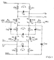
- a first embodiment of a differential amplifier is shown.
- the differential amplifier of Fig. 1 is designed for an operating frequency of preferably 2.4 GHz. It is therefore sufficient that the differential amplifier is designed as Selektiwerschreibr and amplifies a frequency range around the operating frequency.
- the differential amplifier of Fig. 1 has a first positive input I p and a second negative input I n for amplifying a differential signal.
- the differential amplifier of Fig. 1 is designed such that a push-pull signal at the inputs I n and l p is amplified significantly higher than a common to the inputs I n and I p common-mode signal.
- the ratio of the gain of the push-pull signal to the gain of the common-mode signal is also referred to as common-mode rejection. This common mode rejection is required for the differential input p I In order to achieve a suppression of interference that may arise as a switching noise in the digital part of an integrated circuit.
- the differential amplifier of Fig. 1 has a first amplifier stage and a second amplifier stage which are cascaded.
- the first amplifier stage has a first N-channel field effect transistor M1, which is connected to the positive input I p, and a second N-channel field effect transistor M2, which is connected to the negative input I n on.
- the first transistor M1 and the second transistor M2 are connected in gate circuit, wherein the first gate G1 of the first transistor M1 and the second gate G2 of the second transistor M2 are at a substantially constant voltage potential V B1 .
- the gate circuit of Fig. 1 has the advantage that an input capacitance is significantly reduced compared to a source circuit, since with a given transistor width, the source capacitance is smaller than the gate capacitance. Furthermore, the source connection S1, S2 is considerably more robust with respect to an electrostatic discharge than the gate connection G1, G2 of the same transistor M1, M2. Another advantage of the circuit in Fig. 1 is that the desired input resistance of, for example, 50 ohms can be easily adjusted. The input resistance is inversely proportional to the transconductance of the transistor M1, M2. By dopant profiles and the geometry (length, width) of the transistor M1, M2 whose slope can be adjusted application specific.
- a first drain terminal D1 of the first transistor M1 is connected to a resonant circuit.
- a second drain terminal D2 of the second transistor M2 is also connected to the resonant circuit.
- the resonant circuit is connected as a load for the first transistor M1 and the second transistor M2.
- the resonant circuit has a first inductance L 1p and a second inductance L 1n , which are operatively connected to one another via a magnetic coupling M.
- the first inductance L 1p is connected to the first drain terminal D 1 of the first transistor M 1.
- the second inductance L 1n is connected to the second drain terminal D2 of the second transistor M2.
- the first inductance L 1p and the second inductance L 1n are connected to a capacitor C zw , which shorts the electrical connection of the two inductors L 1p , L 1n to ground GND with respect to the operating frequency.
- the resonant circuit has a capacitance C 1 which is connected to the first drain terminal D1 of the first transistor M1 and the first inductor L 1p and to the second drain terminal D2 of the second transistor M2 and the second inductor L 1n connected is.
- the magnetically coupled inductors L 1p , U 1n are designed, for example, as an integrated coil with a center tap. to Integration of these coils can be used with wiring levels of a chip, wherein an insulator (SiO 2 or the like) with a relative permeability of 1 is used within the coil windings.
- the capacitance C 1 is formed for example as an integrated plate capacitor.
- the resonance of the resonant circuit L 1p , L 1n . C 1 is, with the inclusion of further connected impedances, such as the capacitances C Kp and C Kn , tuned to one at the inputs I n and I p , the operating frequency exhibiting push-pull input signal such that the resonant circuit L 1p , L 1n , C 1 for the push-pull input signal at the operating frequency in or near the resonance has an impedance maximum.
- the first amplifier stage with the transistors M1 and M2 in the base circuit reaches a gain maximum.
- the resonant circuit L 1p , L 1n , C 1 is tuned for common mode signals such that the impedance of the resonant circuit L 1p , L 1n , C 1 for these signals is significantly lower than the impedance maximum for push-pull signals of the operating frequency.
- the different impedances for push-pull and common-mode signals are caused, on the one hand, by the fact that the capacitance C1 is ineffective for common-mode signals.
- the inductive coupling M of the first inductance L 1p with the second inductance L 1n causes the common-mode signals in each inductance L 1p , L 1n to be destructively superimposed and thus the resonance-determining inductances L 1p , L 1n to act correspondingly reduced.
- the coupling M is preferably designed such that in push-pull operation, the total inductance in the resonant circuit is increased by twice the value of the inductive coupling M.
- the lower total inductance in common mode operation leads to a higher resonant frequency of the load resonant circuit L 1p , L 1n , C 1 and thus to a lower gain at the operating frequency to which the resonant circuit L 1p , L 1n , C 1 is tuned in push-pull operation.
- the circuit structure of FIG Fig. 1 Achieve common mode rejections from 15dB to 20dB per amplifier stage.
- the circuit of Fig. 1 also has the advantage that can be dispensed with a current source at the source terminals S1 and S2 of the first transistor M1 and the second transistor M2. Such a power source would require an additional voltage drop, which is lost to the amplifier stages and thus reduces the maximum voltage swing. Instead of a current source, the transistors M1 and M2 are connected in source circuit.
- another resonant circuit L 0p , L 0n , C 0 is connected to ground GND.
- two magnetically coupled inductances L 0p and L 0n are provided, wherein the first inductance L 0p is connected to ground GND and to the first source terminal S1 of the first transistor M1.
- the second inductance L 0n is connected to ground GND and to the second source terminal S2 of the second transistor M2.
- this resonant circuit forms an impedance maximum for push-pull signals for the operating frequency.
- the total input impedance of the differential amplifier of the Fig. 1 however limited to this 50 ohms.
- Common mode signals of the operating frequency may be the total input impedance according to the above embodiments to the load impedance lower.
- the circuit of Fig. 1 is formed as a cascaded arrangement of two amplifier stages. Both amplifier stages use the same quiescent current for operating point adjustment.
- the sum of the direct currents flowing through the first transistor M1 and through the second transistor M2 corresponds to the sum of the direct currents flowing through the third transistor M3 and the fourth transistor M4.
- a capacitor C zw both stages are decoupled with respect to the operating frequency, as this capacitor C zw for the operating frequency represents an AC short to ground GND. For constant operating point currents, therefore, a substantially constant intermediate voltage drops across this capacitor C zw .
- the differential output of the first amplifier stage is AC coupled to the differential input of the second amplifier stage of the transistors M3 and M4 via two integrated coupling capacitors C Kp and C Kn .
- the third transistor M3 and the fourth transistor M4 are connected in source circuit.
- the third gate G3 of the third transistor M3 is connected via a high-resistance resistor R3 to a constant voltage source V B2 for operating point adjustment and to the capacitor C Kp for coupling the AC signal.
- the fourth gate G4 of the fourth transistor M4 is connected via a high-resistance resistor R4 to the same constant voltage source V B2 for operating point adjustment and to the capacitor C Kn for coupling the AC signal.
- a further resonant circuit L 2p , L 2n , C 2 is connected as a load. Furthermore, at the third drain terminal D3 of the third transistor M3 is the negative Output O n of the differential amplifier and connected to the fourth drain terminal D4 of the fourth transistor M4, the positive output Op of the differential amplifier.
- the further resonant circuit L 2p , L 2n , C 2 of the second amplifier stage acts as a load analogous to the load resonant circuit L 1p , L 1n , C 1 of the first amplifier stage.
- the further resonant circuit L 2p , L 2n , C 2 has an impedance maximum in its resonance, so that the gain of the second amplification stage for push-pull signals is maximized.
- the impedance is significantly smaller and thus also the gain of these common-mode signals. Both amplifier stages can thus achieve a common mode rejection of 30 dB to 40 dB.
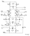
- Fig. 2 shows a second amplifier stage
- the additional to the third transistor M3 and the fourth transistor M4 has a fifth transistor M5 and a sixth transistor M6.
- the fifth transistor M5 is connected to the third transistor M3 to a first cascode arrangement.
- the fourth transistor M4 is connected to the sixth transistor M6 to form a second cascode arrangement.
- the gate terminals G5 and G6 of the fifth transistor M5 and the sixth transistor M6 are connected to a constant voltage source V B2 .
- the drain terminals D5 and D6 of the fifth transistor M5 and the sixth transistor M6 are connected to the further resonant circuit L 2p , L 2n , C 2 and the outputs Op and O n .
- the cascode arrangement has the advantage that a greater gain can be achieved by the second stage. Furthermore, only the transistors M5 and M6 have to have the necessary breakdown voltage resistance for the output voltage swing.
- a third embodiment is in Fig. 3 shown.
- the second amplifier stage has transistors M5 'and M6' in addition to the third transistor M3 and the fourth transistor M4 in the emitter circuit.
- the transistors M5 'and M6' are connected in a neutralization circuit (cross quad) for neutralizing the Miller capacitances.
- the sixth gate terminal G6 of the sixth transistor M6 ' is connected to the fourth gate terminal G4 of the fourth transistor M4.
- the sixth drain terminal D6 of the sixth transistor M6 ' is connected to the third drain terminal D3 of the third transistor M3.
- the fifth gate terminal G5 of the fifth transistor M5 ' is connected to the third gate terminal G3 of the third transistor M3. Furthermore, the fifth drain terminal D5 of the fifth transistor M5 'is connected to the fourth drain terminal D4 of the fourth transistor M4.
- the source terminals S5 and S6 are not connected.
- the embodiment variant Fig. 3 has compared to the embodiment of the Fig. 2 the advantage that at the operating point over the second amplifier stage falling DC voltage is lower, so that a larger output stroke is available at low supply voltages V DD . Furthermore, the embodiment has improved stability over a cascode circuit.
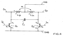
- a first base B1 of a first npn bipolar transistor Q1 is connected to an input Ip of the differential amplifier.
- a second base B2 of a second npn bipolar transistor Q2 is connected to another input I n of Connected differential amplifier.
- the first npn bipolar transistor Q 1 and the second npn bipolar transistor are differentially connected in emitter circuit.
- the collectors K1 and K2 of the two npn bipolar transistors Q1 and Q2 are formed with a resonant circuit of a capacitor C1 and a coil with a center tap whose first inductor L1 p is coupled to the second inductor L1n via the coupling factor M.
- the winding sense of both coil parts is, as in Fig. 4 shown, the same.
- the outputs O n and Op of the single-stage differential amplifier are connected to the collectors K1 and K2 of the npn bipolar transistors Q1 and Q2, respectively.
- This circuit has the advantages of a higher input impedance and a very low supply voltage. Components for operating point adjustment are in Fig. 4 omitted in favor of a simplified presentation.
- P-channel field effect transistors can also be used.
- a mixed use of N-channel field effect transistors and P-channel field effect transistors is advantageous, for example, to use the lower transistor noise of a P-channel field effect transistor in the input amplifier stage.
- a mixed use of field effect transistors and bipolar transistors in one and the same differential amplifier can be interconnected in combination of different basic amplifier circuits. Depending on the type of interconnected differential amplifier basic circuit, the frequency response of the differential amplifier of the application can be adjusted.
Description
Die vorliegende Erfindung betrifft einen Differenzverstärker und ein Funksystem mit einem Differenzverstärker.The present invention relates to a differential amplifier and a radio system with a differential amplifier.
Hochfrequenz-Verstärker werden für eine Vielzahl von Anwendungsfällen benötigt. So dienen Hochfrequenz-Verstärker der Verstärkung von empfangenen oder zu sendenden Radiosignalen. Weiterhin werden Hochfrequenz-Verstärker in Sensorsystemen, in Mobiltelefonen oder Radaranlagen verwendet. Für mehrere Anwendungen ist es dabei ausreichend, dass der Verstärker lediglich ein schmales Frequenzband im Bereich einer Betriebsfrequenz verstärkt. Ein derartiger Verstärker wird auch als Selektivverstärker bezeichnet. Bekannte Verstärkerschaltungen sind beispielsweise der Differenzverstärker.High frequency amplifiers are needed for a variety of applications. Thus, high frequency amplifiers are used to amplify received or to be transmitted radio signals. Furthermore, high-frequency amplifiers are used in sensor systems, in mobile phones or radars. For several applications it is sufficient that the amplifier only amplifies a narrow frequency band in the range of an operating frequency. Such an amplifier is also referred to as a selective amplifier. Known amplifier circuits are, for example, the differential amplifier.
Ein Differenzverstärker ist beispielsweise in "
Aus
Aus der
Aus der
Aus
Aus
Aus
In
Der Erfindung liegt die Aufgabe zu Grunde, für eine Hochfrequenz einen Differenzverstärker mit möglichst verbesserten elektrischen Eigenschaften weiter zu entwickeln. Diese Aufgabe wird durch einen Differenzverstärker mit den Merkmalen des Anspruchs 1 gelöst Eine weitere Aufgabe besteht darin ein Funksystem mit einem möglichst verbesserten Differenzverstärker zu entwickeln. Diese Aufgabe wird durch ein Funksystem mit den Merkmalen des Anspruchs 14 gelöst. Vorteilhafte Weiterbildungen der Erfindung sind Gegenstand von Unteransprüchen.The invention is based on the object of further developing a differential amplifier with as improved electrical properties as possible for a high frequency. This object is achieved by a differential amplifier having the features of claim 1. Another object is to develop a radio system with a differential amplifier that is as improved as possible. This object is achieved by a radio system with the features of claim 14. Advantageous developments of the invention are the subject of dependent claims.
Demzufolge ist ein Differenzverstärker vorgesehen, der eine erste Induktivität aufweist, die mit einer zweiten Induktivität magnetisch gekoppelt ist. Weiterhin weist der Differenzverstärker eine Kapazität auf. Die Kapazität, die erste Induktivität und die zweite Induktivität sind derart zu einem Resonanzkreis verschaltet, dass der Resonanzkreis für ein Gleichtaktsignal eine Gleichtakt-Impedanz und für ein Gegentaktsignal eine von der Gleichtakt-Impedanz verschiedene Gegentakt-Impedanz aufweist.Accordingly, a differential amplifier is provided, which has a first inductance, which is magnetically coupled to a second inductance. Furthermore, the differential amplifier has a capacity. The capacitance, the first inductor and the second inductor are connected in a resonant circuit such that the common mode resonant circuit has a common mode impedance and, for a push-pull signal, a common mode impedance different from the common mode impedance.
Unter einem Gleichtaktsignal wird dabei ein Signal verstanden, dass an beiden Eingängen des Differenzverstärkers mit gleicher Frequenz und gleicher Phasenlage und gleicher Amplitude anliegt. Unter einem Gegentaktsignal wird ein an den Eingängen anliegendes Signal mit gleicher Frequenz, gleicher Amplitude und einer um 180° verschobenen Phase verstanden. Gleichtaktsignale und Gegentaktsignale können auch einander überlagert sein. Das Gegentaktsignal ist dabei üblicherweise das Nutzsignal. Zur Ausbildung der Resonanz für das Gleichtaktsignal werden bei deren Auslegung vorzugsweise eine effektive Eingangsimpedanz einer nachfolgenden Stufe und/oder beeinflussende parasitäre Impedanzen berücksichtigt. Vorteilhafterweise ist der Differenzverstärker als Selektivverstärker zur Verstärkung von Signalen einer oder mehrerer Betriebsfrequenzen ausgebildet. Vorzugsweise ist dabei die Resonanz des Resonanzkreises auf zumindest eine Betriebsfrequenz, insbesondere 2,4 GHz, abgestimmt. Der Resonanzkreis kann auch als Schwingkreis bezeichnet werden. Vorteilhafterweise sind die erste Induktivität und die zweite Induktivität im Rahmen der Fertigungstoleranzen gleich ausgebildet.In this case, a common-mode signal is understood to mean a signal which is applied to both inputs of the differential amplifier with the same frequency and the same phase position and the same amplitude. A push-pull signal is understood to be a signal present at the inputs with the same frequency, the same amplitude and a phase shifted by 180 °. Common-mode signals and push-pull signals can also be superimposed on one another. The push-pull signal is usually the useful signal. In order to form the resonance for the common-mode signal, an effective input impedance of a subsequent stage and / or influencing parasitic impedances are preferably taken into account in their design. Advantageously, the differential amplifier is designed as a selective amplifier for amplifying signals of one or more operating frequencies. Preferably, the resonance of the resonant circuit is tuned to at least one operating frequency, in particular 2.4 GHz. The resonant circuit can also be referred to as a resonant circuit. Advantageously, the first inductance and the second inductance are the same in the context of manufacturing tolerances.
Bevorzugt ist der Differenzverstärker zur Verstärkung von Hochfrequenzsignalen ausgebildet, wobei unter Hochfrequenz ein Bereich verstanden wird, in dem das transiente Verhalten der Transistoren wesentlich durch parasitäre Impedanzen, insbesondere durch den Miller-Effekt beeinflusst wird.Preferably, the differential amplifier is designed to amplify high-frequency signals, wherein high-frequency is understood to mean a range in which the transient behavior of the transistors is significantly influenced by parasitic impedances, in particular by the Miller effect.
Es sind ein erster Transistor und ein zweiter Transistor vorgesehen, wobei der Resonanzkreis mit dem ersten Transistor und dem zweiten Transistor derart verbunden ist, dass der Resonanzkreis eine insbesondere symmetrische Last für den ersten Transistor und für den zweiten Transistor ausbildet. Vorteilhafterweise sind der erste Transistor und der zweite Transistor im Rahmen der Fertigungstoleranzen gleich ausgebildet (engl. matching). Vorzugsweise ist die Verstärkung durch den ersten Transistor und den zweiten Transistor von der Höhe der Impedanz abhängig.There are provided a first transistor and a second transistor, wherein the resonant circuit is connected to the first transistor and the second transistor such that the resonant circuit forms a particular symmetrical load for the first transistor and for the second transistor. Advantageously, the first transistor and the second transistor are of the same design within the scope of the manufacturing tolerances (matching). Preferably, the gain by the first transistor and the second transistor is dependent on the magnitude of the impedance.
Der erste Transistor und der zweite Transistor sind in Gateschaltung (dt. auch Torschaltung) verschaltet. Werden anstelle von Feldeffekttransistoren Bipolartransistoren verwendet, sind diese in Basisschaltung verschaltet. In der Gateschaltung sind die Gate-Anschlüsse (dt. auch Tor-Anschluss) mit einer konstanten Spannungsquelle verbunden und somit bezüglich des zu verstärkenden Signals gegen Masse wechselspannungsmäßig kurzgeschlossen. In der Basisschaltung sind die Basen des ersten Transistors und des zweiten Transistors mit einer Konstant-Spannungsquelle verbunden und somit ebenfalls wechselspannungsmäßig nach Masse kurzgeschlossen. Der Resonanzkreis ist in jeder dieser Weiterbildungen die Last der differentiell verschalteten Transistoren.The first transistor and the second transistor are connected in gate circuit (ie also gate circuit). If bipolar transistors are used instead of field effect transistors, these are interconnected in basic circuit. In the gate circuit, the gate terminals (ie also gate terminal) are connected to a constant voltage source and thus with respect to the signal to be amplified to ground AC voltage shorted. In the base circuit, the bases of the first transistor and the second transistor are connected to a constant voltage source and thus also AC-shorted to ground. The resonant circuit in each of these developments is the load of the transistors connected in different ways.
Ein erster Source-Anschluss (dt. auch Quelle-Anschluss) beziehungsweise ein erster Emitter-Anschluss des ersten Transistors ist mit einem ersten Eingang des Differenzverstärkers und ein zweiter Source-Anschluss beziehungsweise ein zweiter Emitteranschluss des zweiten Transistors ist mit einem zweiten Eingang des Differenzverstärkers verbunden. Bevorzugt sind mit diesen Eingangstransistoren dabei keine Stromquelle oder Stromsenke verbunden.A first source terminal (dt also source terminal) or a first emitter terminal of the first transistor is connected to a first input of the differential amplifier and a second source terminal or a second emitter terminal of the second transistor is connected to a second input of the differential amplifier , In this case, no current source or current sink are preferably connected to these input transistors.
Gemäß einer bevorzugten Ausgestaltung sind eine Steilheit des ersten Transistors und eine Steilheit des zweiten Transistors zur Bildung einer Eingangsimpedanz des Differenzverstärkers von 50 Ohm ausgebildet. Vorzugsweise sind die Geometrien (Kanalbreite/Kanallänge) und/oder das Dotierprofil an die Anforderungen der Eingangsimpedanz angepasst. Vorteilhafterweise ist der erste Source-Anschluss beziehungsweise der erste Emitter-Anschluss des ersten Transistors und der zweite Source-Anschluss beziehungsweise der zweite Emitteranschluss des zweiten Transistors mit einem weiteren Resonanzkreis des Differenzverstärkers verbunden. Vorzugsweise bildet der weitere Resonanzkreis eine Gleichtakt-Eingangsimpedanz und eine Gegentakt-Eingangsimpedanz, um das Gegentakt-Eingangssignal geringer zu Dämpfen als das Gleichtakt-Eingangssignal.According to a preferred embodiment, a transconductance of the first transistor and a transconductance of the second transistor for forming an input impedance of the differential amplifier of 50 ohms are formed. The geometries (channel width / channel length) and / or the doping profile are preferably matched to the requirements of the input impedance. Advantageously, the first source terminal or the first emitter terminal of the first transistor and the second source terminal or the second emitter terminal of the second transistor is connected to a further resonant circuit of the differential amplifier. Preferably, the further resonant circuit forms a common mode input impedance and a push-pull input impedance to attenuate the push-pull input signal less than the common mode input signal.
In einer vorteilhaften Ausgestaltung der Erfindung ist für das Gegentaktsignal die Resonanzfrequenz beider Resonanzkreise im Rahmen der Fertigungstoleranzen gleich (engl. matching).In an advantageous embodiment of the invention, the resonant frequency of both resonant circuits within the manufacturing tolerances is the same for the push-pull signal (English: matching).
Bevorzugt sind die erste Induktivität und die zweite Induktivität durch symmetrische Spulenwicklungen gebildet. Der Wickelsinn bestimmt dabei das Vorzeichen der magnetischen Kopplung. Die magnetische Kopplung ist bei einer symmetrischen Spulenwicklung vorzugsweise positiv.The first inductance and the second inductance are preferably formed by symmetrical coil windings. The winding sense determines the sign of the magnetic coupling. The magnetic coupling is preferably positive for a symmetrical coil winding.
Gemäß einer besonders bevorzugten Ausgestaltung der Erfindung ist vorgesehen, dass die erste Induktivität und die zweite Induktivität durch eine integrierte Spule mit Mittelabgriff gebildet sind.According to a particularly preferred embodiment of the invention it is provided that the first inductance and the second inductance are formed by an integrated coil with center tap.
Um die Erfindung vorteilhaft auszugestalten sind die erste Induktivität und die zweite Induktivität derart magnetisch gekoppelt, dass sich für Gleichtaktsignale das durch einen Laststrom durch die erste Induktivität abfallende Spannungssignal und das induzierte Spannungssignal destruktiv überlagern. Hingegen überlagern sich das durch einen Laststrom durch die erste Induktivität abfallende Spannungssignal und das induzierte Spannungssignal für Gegentaktsignale konstruktiv. Das induzierte Spannungssignal wird dabei durch ein Magnetfeld induziert, das von der zweiten Induktivität erzeugt ist. Dasselbe gilt natürlich auch für den umgekehrten Fall, in dem in der zweiten Induktivität ein Spannungssignal induziert wird.In order to design the invention advantageously, the first inductor and the second inductor are magnetically coupled in such a way that, for common-mode signals, the voltage signal falling through a load current through the first inductor and the induced voltage signal are destructively superimposed. On the other hand, the voltage signal falling through the first inductance due to a load current and the induced voltage signal for push-pull signals overlap constructively. The induced voltage signal is thereby induced by a magnetic field generated by the second inductor. The same naturally also applies to the reverse case, in which a voltage signal is induced in the second inductance.
Gemäß einer vorteilhaften Weiterbildung der Erfindung weist der Differenzverstärker zwei kaskadierte Verstärkerstufen auf. Dabei weist eine erste Verstärkerstufe den ersten Transistor und den zweiten Transistor auf. Eine zweite Verstärkerstufe weist einen dritten Transistor und einen vierten Transistor auf. Vorzugsweise sind die erste Verstärkerstufe und die zweite Verstärkerstufe durch einen identischen Betriebsstrom betrieben, der sowohl durch die erste Verstärkerstufe als auch durch die zweite Verstärkerstufe fließt. Vorteilhafterweise sind der dritte Transistor und der vierte Transistor im Rahmen der Fertigungstoleranzen gleich ausgebildet (engl. matching). Gemäß einer vorteilhaften Weiterbildung ist vorgesehen, dass der dritte Transistor und der vierte Transistor jeweils in Sourceschaltung (dt. auch Quellenschaltung) beziehungsweise in Emitterschaltung verschaltet sind. Bevorzugt ist ein dritter Gate-Anschluss beziehungsweise ein dritter Basis-Anschluss des dritten Transistors über eine erste Koppel-Kapazität mit dem ersten Drain-Anschluss (dt. auch Senken-Anschluss) beziehungsweise mit dem ersten Kollektor-Anschluss des ersten Transistors verbunden. Ebenfalls bevorzugt ist ein vierter Gate-Anschluss beziehungsweise ein vierter Basis-Anschluss des vierten Transistors über eine zweite Koppel-Kapazität mit dem zweiten Drain-Anschluss beziehungsweise mit dem zweiten Kollektor-Anschluss des zweiten Transistors verbunden.According to an advantageous development of the invention, the differential amplifier has two cascaded amplifier stages. In this case, a first amplifier stage to the first transistor and the second transistor. A second amplifier stage comprises a third transistor and a fourth transistor. Preferably, the first amplifier stage and the second amplifier stage are operated by an identical operating current flowing through both the first amplifier stage and the second amplifier stage. Advantageously, the third transistor and the fourth transistor are identical within the scope of the manufacturing tolerances (matching). According to an advantageous development, it is provided that the third transistor and the fourth transistor are respectively connected in source circuit (also source circuit) or in emitter circuit. Preferably, a third gate terminal or a third base terminal of the third transistor is connected via a first coupling capacitance to the first drain terminal (also dc terminal) or to the first collector terminal of the first transistor. Also preferably, a fourth gate terminal or a fourth base terminal of the fourth transistor is connected via a second coupling capacitance to the second drain terminal and to the second collector terminal of the second transistor.
In einer Weiterbildung sind ein fünfter Transistor und eine sechster Transistor vorgesehen. Der fünfte Transistor ist mit dem dritten Transistor zu einer ersten Kaskodestufe verbunden. Der sechste Transistor ist mit dem vierten Transistor zu einer zweiten Kaskodestufe verbunden.In a further development, a fifth transistor and a sixth transistor are provided. The fifth transistor is connected to the third transistor to a first cascode stage. The sixth transistor is connected to the fourth transistor to a second cascode stage.
In einer anderen Weiterbildung sind Kapazitäten zur Neutralisation der Millerkapazitäten des dritten Transistors und des vierten Transistors vorgesehen. Bevorzugt sind ein fünfter Transistor und ein sechster Transistor als Kapazitäten zur Neutralisation vorgesehen. Der fünfte Transistor ist mit dem dritten Transistor und dem vierten Transistor zur Neutralisation der Millerkapazität des dritten Transistors verbunden. Der sechste Transistor ist mit dem vierten Transistor und dem dritten Transistor zur Neutralisation der Millerkapazität des vierten Transistors verbunden.In another development, capacities for neutralizing the Millerkapazitäten the third transistor and the fourth transistor are provided. Preferably, a fifth transistor and a sixth transistor are provided as capacities for neutralization. The fifth transistor is connected to the third transistor and the fourth transistor for neutralizing the Millerkapazität of the third transistor. The sixth transistor is connected to the fourth transistor and the third transistor for neutralizing the Millerkapazität of the fourth transistor.
Gemäß einer besonders vorteilhaften Weiterbildung der Erfindung ist ein wiederum weiterer Resonanzkreis als Last der zweiten Verstärkerstufe vorgesehen. Der Resonanzkreis ist mit dem dritten Transistor und dem vierten Transistor verbunden, sofern keine Kaskodestufe verwendet wird. Andernfalls ist der weitere Resonanzkreis mit dem fünften Transistor und dem sechsten Transistor zur Ausbildung der zweiten Verstärkerstufe verbunden.According to a particularly advantageous embodiment of the invention, a turn further resonant circuit is provided as a load of the second amplifier stage. The resonant circuit is connected to the third transistor and the fourth transistor, unless a cascode stage is used. Otherwise, the further resonant circuit with the fifth transistor and the sixth transistor for forming the second amplifier stage connected.
Die der Erfindung zu Grunde liegende Aufgabe wird weiterhin durch ein Funksystem gelöst. Das Funksystem weist vorzugsweise Sende- und Empfangseinheiten zur Kommunikation auf. Das Funksystem weist einen zuvor erläuterten Differenzverstärker zur Verstärkung einer Übertragungsfrequenz auf. Die Übertragungsfrequenz beträgt vorteilhafterweise 2,4 GHz. Der Differenzverstärker weist vorteilhafterweise eine erste Induktivität, die mit einer zweiten Induktivität magnetisch gekoppelt ist, und eine Kapazität auf.The object underlying the invention is further achieved by a radio system. The radio system preferably has transmitting and receiving units for communication. The radio system has a previously explained differential amplifier for amplifying a transmission frequency. The transmission frequency is advantageously 2.4 GHz. The differential amplifier advantageously has a first inductance, which is magnetically coupled to a second inductance, and a capacitance.
Die Kapazität, die erste Induktivität und die zweite Induktivität sind vorzugsweise derart zu einem Resonanzkreis verschaltet, dass der Resonanzkreis für ein Gleichtaktsignal der Übertragungsfrequenz eine Gleichtakt-Impedanz aufweist. Weiterhin weist der Resonanzkreis für ein Gegentaktsignal eine von der Gleichtakt-Impedanz verschiedene Gegentakt-Impedanz auf.The capacitance, the first inductance and the second inductance are preferably connected in such a way to a resonant circuit, that the resonant circuit for a common-mode signal of the transmission frequency has a common-mode impedance. Furthermore, the resonant circuit for a push-pull signal has a push-pull impedance different from the common-mode impedance.
Im Folgenden wird die Erfindung in Ausführungsbeispielen anhand von Zeichnungen näher erläutert.In the following the invention will be explained in more detail in exemplary embodiments with reference to drawings.
Dabei zeigen
- Fig. 1
- einen ersten Schaltkreis eines Differenzverstärkers,
- Fig. 2
- einen zweiten Schaltkreis eines Differenzverstärkers mit zwei Kaskodeanordnungen,
- Fig. 3
- einen dritten Schaltkreis eines Differenzverstärkers mit einer Neutralisation der Millerkapazitäten, und
- Fig. 4
- einen vierten Schaltkreis eines Differenzverstärkers mit differentiellen npn-Bipolartransistoren in Emitterschaltung.
- Fig. 1
- a first circuit of a differential amplifier,
- Fig. 2
- a second circuit of a differential amplifier with two cascode arrangements,
- Fig. 3
- a third circuit of a differential amplifier with a neutralization of the Millerkapazitäten, and
- Fig. 4
- a fourth circuit of a differential amplifier with differential npn bipolar transistors in emitter circuit.
In
Der Differenzverstärker der
Der Differenzverstärker der
Die Gate-Schaltung der
Ein erster Drain-Anschluss D1 des ersten Transistor M1 ist mit einem Resonanzkreis verbunden. Ein zweiter Drain-Anschluss D2 des zweiten Transistor M2 ist ebenfalls mit dem Resonanzkreis verbunden. Der Resonanzkreis ist dabei als Last für den ersten Transistor M1 und den zweiten Transistor M2 verschaltet. Der Resonanzkreis weist eine erste Induktivität L1p und eine zweite Induktivität L1n auf, die über eine magnetische Kopplung M miteinander wirkverbunden sind.A first drain terminal D1 of the first transistor M1 is connected to a resonant circuit. A second drain terminal D2 of the second transistor M2 is also connected to the resonant circuit. The resonant circuit is connected as a load for the first transistor M1 and the second transistor M2. The resonant circuit has a first inductance L 1p and a second inductance L 1n , which are operatively connected to one another via a magnetic coupling M.
Die erste Induktivität L1p ist mit dem ersten Drain-Anschluss D1 des ersten Transistors M1 verbunden. Die zweite Induktivität L1n ist mit dem zweiten Drain-Anschluss D2 des zweiten Transistors M2 verbinden. Weiterhin sind die erste Induktivität L1p und die zweite Induktivität L1n mit einem Kondensator Czw verbunden, der die elektrische Verbindung der beiden Induktivitäten L1p, L1n nach Masse GND bezüglich der Betriebsfrequenz kurzschließt. Weiterhin weist der Resonanzkreis eine Kapazität C1 auf, der zum einen mit dem ersten Drain-Anschluss D1 des ersten Transistors M1 und der ersten Induktivität L1p und zum anderen mit dem zweiten Drain-Anschluss D2 des zweiten Transistors M2 und der zweiten Induktivität L1n verbunden ist. Die magnetisch gekoppelten Induktivitäten L1p, U1n sind beispielsweise als integrierte Spule mit Mittelabgriff ausgebildet. Zur Integration dieser Spulen können Verdrahtungsebenen eines Chips verwendet werden, wobei innerhalb der Spulenwicklungen ein Isolator (SiO2 oder dergleichen) mit einer relativen Permeabilität von 1 verwendet wird. Die Kapazität C1 ist beispielsweise als integrierter Plattenkondensator ausgebildet.The first inductance L 1p is connected to the first drain terminal D 1 of the first transistor M 1. The second inductance L 1n is connected to the second drain terminal D2 of the second transistor M2. Furthermore, the first inductance L 1p and the second inductance L 1n are connected to a capacitor C zw , which shorts the electrical connection of the two inductors L 1p , L 1n to ground GND with respect to the operating frequency. Furthermore, the resonant circuit has a capacitance C 1 which is connected to the first drain terminal D1 of the first transistor M1 and the first inductor L 1p and to the second drain terminal D2 of the second transistor M2 and the second inductor L 1n connected is. The magnetically coupled inductors L 1p , U 1n are designed, for example, as an integrated coil with a center tap. to Integration of these coils can be used with wiring levels of a chip, wherein an insulator (SiO 2 or the like) with a relative permeability of 1 is used within the coil windings. The capacitance C 1 is formed for example as an integrated plate capacitor.
Die Resonanz des Resonanzkreises L1p, L1n. C1 ist unter Einbeziehung weiterer angeschlossener Impedanzen, wie beispielsweise die Kapazitäten CKp und CKn, auf ein an den Eingängen In und Ip anliegendes, die Betriebsfrequenz aufweisendes Gegentakt-Eingangssignal derart abgestimmt, dass der Resonanzkreis L1p, L1n, C1 für das Gegentakt-Eingangssignal auf der Betriebsfrequenz in oder nahe der Resonanz ein Impedanzmaximum aufweist. Für das Impedanzmaximum erreicht die erste Verstärkerstufe mit den Transistoren M1 und M2 in Basisschaltung ein Verstärkungsmaximum.The resonance of the resonant circuit L 1p , L 1n . C 1 is, with the inclusion of further connected impedances, such as the capacitances C Kp and C Kn , tuned to one at the inputs I n and I p , the operating frequency exhibiting push-pull input signal such that the resonant circuit L 1p , L 1n , C 1 for the push-pull input signal at the operating frequency in or near the resonance has an impedance maximum. For the impedance maximum, the first amplifier stage with the transistors M1 and M2 in the base circuit reaches a gain maximum.
Dagegen ist der Resonanzkreis L1p, L1n, C1 für Gleichtaktsignale derart abgestimmt, dass die Impedanz des Resonanzkreises L1p, L1n, C1 für diese Signale signifikant geringer ist als das Impedanzmaximum für Gegentaktsignale der Betriebsfrequenz. Die unterschiedlichen Impedanzen für Gegentakt- und Gleichtaktsignale werden zum einen dadurch bewirkt, dass die Kapazität C1 für Gleichtaktsignale wirkungslos ist. Weiterhin bewirkt die induktive Kopplung M der ersten Induktivität L1p mit der zweiten Induktivität L1n dass sich die Gleichtaktsignale in jeder Induktivität L1p, L1n destruktiv überlagern und somit die resonanzbestimmenden Induktivitäten L1p, L1n entsprechend reduziert wirken. Die Kopplung M ist vorzugsweise derart ausgebildet sein, dass im Gegentaktbetrieb die Gesamtinduktivität im Resonanzkreis um den zweifachen Wert der induktiven Kopplung M erhöht ist.In contrast, the resonant circuit L 1p , L 1n , C 1 is tuned for common mode signals such that the impedance of the resonant circuit L 1p , L 1n , C 1 for these signals is significantly lower than the impedance maximum for push-pull signals of the operating frequency. The different impedances for push-pull and common-mode signals are caused, on the one hand, by the fact that the capacitance C1 is ineffective for common-mode signals. Furthermore, the inductive coupling M of the first inductance L 1p with the second inductance L 1n causes the common-mode signals in each inductance L 1p , L 1n to be destructively superimposed and thus the resonance-determining inductances L 1p , L 1n to act correspondingly reduced. The coupling M is preferably designed such that in push-pull operation, the total inductance in the resonant circuit is increased by twice the value of the inductive coupling M.
Im Gegentaktbetrieb ist die Gesamtinduktivität ![]()
und im Gleichtaktbetrieb ![]()
![]()
and in common mode operation ![]()
Die geringere Gesamtinduktivität im Gleichtaktbetrieb führt zu einer höheren Resonanzfrequenz des Lastschwingkreises L1p, L1n, C1 und damit zu einer geringeren Verstärkung bei der Betriebsfrequenz, auf die der Resonanzkreis L1p, L1n, C1 bei Gegentaktbetrieb abgestimmt ist. Bei geringen Spulengüten von 5 bis 6, die für integrierte Induktivitäten L1p und L1n erzielbar sind, lassen sich durch den Schaltungsaufbau der
Die Schaltung der
Parallel zu den Eingängen ist ein weiterer Resonanzkreis L0p, L0n, C0 gegen Masse GND geschaltet. Wiederum sind zwei magnetisch gekoppelte Induktivitäten L0p und L0n vorgesehen, wobei die erste Induktivität L0p mit Masse GND und mit dem ersten Source-Anschluss S1 des ersten Transistors M1 verbunden ist. Die zweite Induktivität L0n ist mit Masse GND und mit dem zweiten Source-Anschluss S2 des zweiten Transistors M2 verbunden. Wiederum bildet dieser Resonanzkreis ein Impedanzmaximum für Gegentaktsignale für die Betriebsfrequenz aus. Durch die Parallelschaltung der Eingangsimpedanz von 50 Ohm des ersten Transistors M1 und des zweiten Transistors M2 ist die Gesamt-Eingangsimpedanz des Differenzverstärkers der
Die Schaltung der
Der differentielle Ausgang der ersten Verstärkerstufe ist mit dem differentiellen Eingang der zweiten Verstärkerstufe aus den Transistoren M3 und M4 über zwei integrierte Koppelkondensatoren CKp und CKn wechselspannungsmäßig gekoppelt. Der dritte Transistor M3 und der vierte Transistor M4 sind in Source-Schaltung verschaltet. Das dritte Gate G3 des dritten Transistors M3 ist über einen hochohmigen Widerstand R3 mit einer Konstantspannungsquelle VB2 zur Arbeitspunkteinstellung und mit dem Kondensator CKp zur Einkopplung des Wechselspannungs-Signals verbunden. Das vierte Gate G4 des vierten Transistors M4 ist über einen hochohmigen Widerstand R4 mit derselben Konstantspannungsquelle VB2 zur Arbeitspunkteinstellung und mit dem Kondensator CKn zur Einkopplung des Wechselspannungs-Signals verbunden.The differential output of the first amplifier stage is AC coupled to the differential input of the second amplifier stage of the transistors M3 and M4 via two integrated coupling capacitors C Kp and C Kn . The third transistor M3 and the fourth transistor M4 are connected in source circuit. The third gate G3 of the third transistor M3 is connected via a high-resistance resistor R3 to a constant voltage source V B2 for operating point adjustment and to the capacitor C Kp for coupling the AC signal. The fourth gate G4 of the fourth transistor M4 is connected via a high-resistance resistor R4 to the same constant voltage source V B2 for operating point adjustment and to the capacitor C Kn for coupling the AC signal.
An dem dritten Drain-Anschluss D3 des dritten Transistors M3 und an dem vierten Drain-Anschluss D4 des vierten Transistors M4 ist wiederum ein weiterer Resonanzkreis L2p, L2n, C2 als Last angeschlossen. Weiterhin ist an dem dritten Drain-Anschluss D3 des dritten Transistors M3 der negative Ausgang On des Differenzverstärkers und an dem vierten Drain-Anschluss D4 des vierten Transistors M4 der positive Ausgang Op des Differenzverstärkers angeschlossen.At the third drain terminal D3 of the third transistor M3 and at the fourth drain terminal D4 of the fourth transistor M4, in turn, a further resonant circuit L 2p , L 2n , C 2 is connected as a load. Furthermore, at the third drain terminal D3 of the third transistor M3 is the negative Output O n of the differential amplifier and connected to the fourth drain terminal D4 of the fourth transistor M4, the positive output Op of the differential amplifier.
Der weitere Resonanzkreis L2p, L2n, C2 der zweiten Verstärkerstufe wirkt als Last analog dem Lastschwingkreis L1p, L1n, C1 der ersten Verstärkerstufe. Für Gegentaktsignale der Betriebsfrequenz weist der weitere Resonanzkreis L2p, L2n, C2 in seiner Resonanz ein Impedanzmaximum auf, so dass die Verstärkung der zweiten Verstärkungsstufe für Gegentaktsignale maximiert ist. Hingegen ist für Gleichtaktsignale die Impedanz signifikant kleiner und somit auch die Verstärkung dieser Gleichtaktsignale. Durch beide Verstärkerstufen kann somit eine Gleichtaktunterdrückung von 30dB bis 40dB erzielt werden.The further resonant circuit L 2p , L 2n , C 2 of the second amplifier stage acts as a load analogous to the load resonant circuit L 1p , L 1n , C 1 of the first amplifier stage. For push-pull signals of the operating frequency, the further resonant circuit L 2p , L 2n , C 2 has an impedance maximum in its resonance, so that the gain of the second amplification stage for push-pull signals is maximized. On the other hand, for common-mode signals, the impedance is significantly smaller and thus also the gain of these common-mode signals. Both amplifier stages can thus achieve a common mode rejection of 30 dB to 40 dB.
Um gegebenenfalls Rückwirkungen der Miller-Kapazität des dritten Transistors M3 und des vierten Transistors M4 zu reduzierten, sind in den
Die Drain-Anschlüsse D5 und D6 des fünften Transistors M5 und des sechsten Transistors M6 sind mit dem weiteren Resonanzkreis L2p, L2n, C2 und den Ausgängen Op und On verbunden. Zusätzlich zur Verhinderung des Miller-Effektes hat die Kaskodeanordnung den Vorteil inne, dass eine größere Verstärkung durch die zweite Stufe erzielbar ist. Weiterhin müssen lediglich die Transistoren M5 und M6 für den Ausgangsspannungshub die notwendige Durchbruchspannungsfestigkeit aufweisen.The drain terminals D5 and D6 of the fifth transistor M5 and the sixth transistor M6 are connected to the further resonant circuit L 2p , L 2n , C 2 and the outputs Op and O n . In addition to preventing the Miller effect, the cascode arrangement has the advantage that a greater gain can be achieved by the second stage. Furthermore, only the transistors M5 and M6 have to have the necessary breakdown voltage resistance for the output voltage swing.
Ein drittes Ausführungsbeispiel ist in
Die Ausführungsvariante aus
Eine nicht beanspruchte Schaltung ist in
Alternativ zu den in den
Claims (14)
- A differential amplifier- with a first inductor (L1p) and a second inductor (L1n), and- with a capacitor (C1),- in which the capacitor (C1), the first inductor (L1p) and the second inductor (L1n) are connected in a resonance circuit (C1, L1p, L1n) in such a way that the resonance circuit (C1, L1p, L1n) has a common-mode impedance for a common-mode signal and a differential-mode impedance different from the common-mode impedance for a differential-mode signal,- in which a first transistor (M1) and a second transistor (M2) are connected in a gate circuit or base circuit for amplification in a frequency range around an operating frequency,- in which the resonance circuit (C1, L1p, L1n) is connected to the first transistor (M1) and the second transistor (M2) in such a way that the resonance circuit (C1, L1p, L1n) forms a symmetrical load for the first transistor (M1) and for the second transistor (M2),- in which a first source terminal (S1) or a first emitter terminal of the first transistor (M1) is connected to a first input (Ip) of the differential amplifier and in which a second source terminal (S2) or a second emitter terminal of the second transistor (M2) is connected to a second input (In) of the differential amplifier,characterized in that
the first inductor and the second inductor are coupled magnetically in such a way that the voltage signal decreasing by a load current through the first inductor and the induced voltage signal produced by the magnetic field generated by the second inductor are superimposed in a destructive manner for common-mode signals and in a constructive manner for differential-mode signals, so that for the common-mode rejection for the operating frequency the common-mode impedance is lower than the differential-mode impedance. - A differential amplifier according to Claim 1, in which a transconductance of the first transistor (M1) and a transconductance of the second transistor (M2) are designed within the scope of manufacturing tolerances in order to form an input impedance of the differential amplifier of 50 Ω.
- A differential amplifier according to any one of the preceding Claims, in which a first source terminal (S1) or a first emitter terminal of the first transistor (M1) and a second source terminal (S2) or a second emitter terminal of the second transistor (M2) are connected to a further resonance circuit (C1, L1p, L1n) of the differential amplifier.
- A differential amplifier according to Claim 3, in which the resonance frequency of the two resonance circuits ([C0, L0p, L0n], [C1, L1p, L1n]) is the same within the scope of manufacturing tolerances for the differential-mode signal.
- A differential amplifier according to any one of the preceding Claims, in which the first inductor (L0p, L1p, L2p) and the second inductor (L0n, L1n, L2n) are formed by symmetrical coil windings.
- A differential amplifier according to any one of the preceding Claims, in which the first inductor (L0p, L1p, L2p) and the second inductor (L0n, L1n, L2n) are formed by an integrated coil with a centre tap.
- A differential amplifier according to any one of the preceding Claims, which is designed in the form of a selective amplifier in order to amplify an operating frequency, wherein a resonance of the resonance circuit ([C0, L0p, L0n], [C1, L1p, L1n], [C2, L2p, L2n]) corresponds within the scope of manufacturing tolerances to the operating frequency of 2.4 GHz.
- A differential amplifier according to any one of the preceding Claims, with two cascaded amplifier stages,- in which the first amplifier stage has the first transistor (M1) and the second transistor (M2),- in which the second amplifier stage has a third transistor (M3) and a fourth transistor (M4),- in which the first amplifier stage and the second amplifier stage are operated by an identical operating current which flow both through the first amplifier stage and through the second amplifier stage.
- A differential amplifier according to Claim 8,- in which the third transistor (M3) and the fourth transistor (M4) are in each case connected in a source circuit or in an emitter circuit,- in which a third gate terminal (G3) or a third base terminal of the third transistor (M3) is connected by way of a first coupling capacitor (CKp) to the first drain terminal (D1) or to the first collector terminal of the first transistor (M1), and- in which a fourth gate terminal (G4) or a fourth base terminal of the fourth transistor (M4) is connected by way of a second coupling capacitor (CKn) to the second drain terminal (D2) or to the second collector terminal of the second transistor (M2).
- A differential amplifier according to one of Claims 8 or 9,- with a fifth transistor (M5) which is connected to the third transistor (M3) to form a first cascode stage,- with a sixth transistor (M6) which is connected to the fourth transistor (M4) to form a second cascode stage.
- A differential amplifier according to one of Claims 8 or 9,- with a first neutralization capacitor (M5') which is connected to the third transistor (M3) and the fourth transistor (M4) in order to neutralize the Miller capacitance of the third transistor (M3), and- with a second neutralization capacitor (M6') which is connected to the fourth transistor (M4) and the third transistor (M3) in order to neutralize the Miller capacitance of the fourth transistor (M4).
- A differential amplifier according to Claim 11, in which- the first neutralization capacitor is formed by a fifth transistor (M5'), and- the second neutralization capacitor is formed by a sixth transistor (M6').
- A differential amplifier according to any one of Claims 8 to 11, with in turn a further resonance circuit (C2, L2p, L2n) in the form of a load of the second amplifier stage, wherein the resonance circuit (C2, L2p, L2n) is connected to the third transistor (M3) and the fourth transistor (M4) or to the fifth transistor (M5) and the sixth transistor (M6) to form the second amplifier stage.
- A radio system for communication, which has a differential amplifier according to any one of the preceding Claims for the amplification of a transmission frequency of 2.4 GHz.
Applications Claiming Priority (1)
| Application Number | Priority Date | Filing Date | Title |
|---|---|---|---|
| DE102006004952A DE102006004952A1 (en) | 2006-02-01 | 2006-02-01 | Differential amplifier and radio system with differential amplifier |
Publications (3)
| Publication Number | Publication Date |
|---|---|
| EP1816742A2 EP1816742A2 (en) | 2007-08-08 |
| EP1816742A3 EP1816742A3 (en) | 2008-06-04 |
| EP1816742B1 true EP1816742B1 (en) | 2013-07-03 |
Family
ID=37982450
Family Applications (1)
| Application Number | Title | Priority Date | Filing Date |
|---|---|---|---|
| EP07001562.3A Active EP1816742B1 (en) | 2006-02-01 | 2007-01-25 | Differential amplifier and radio system with differential amplifier |
Country Status (3)
| Country | Link |
|---|---|
| US (1) | US7521996B2 (en) |
| EP (1) | EP1816742B1 (en) |
| DE (1) | DE102006004952A1 (en) |
Families Citing this family (18)
| Publication number | Priority date | Publication date | Assignee | Title |
|---|---|---|---|---|
| US7649416B2 (en) * | 2007-09-27 | 2010-01-19 | Nanoamp Mobile, Inc. | Load inductor sharing |
| US7705682B2 (en) * | 2007-09-27 | 2010-04-27 | Nanoamp Mobile, Inc. | Inductor sharing in radio frequency communications |
| KR20090090928A (en) * | 2008-02-22 | 2009-08-26 | 삼성전자주식회사 | Low noise amplifier |
| JP2011066570A (en) * | 2009-09-16 | 2011-03-31 | Toshiba Corp | Semiconductor integrated circuit |
| WO2012088517A1 (en) | 2010-12-23 | 2012-06-28 | Marvell World Trade Ltd | Cmos push-pull power amplifier with even-harmonic cancellation |
| FR2974957B1 (en) * | 2011-05-05 | 2013-06-07 | Commissariat Energie Atomique | AMPLIFICATION CIRCUIT AND RECEIVING CHAIN |
| US8604876B2 (en) * | 2011-05-13 | 2013-12-10 | Qualcomm, Incorporated | Current buffer |
| RU2465720C1 (en) * | 2011-11-08 | 2012-10-27 | Федеральное государственное бюджетное образовательное учреждение высшего профессионального образования "Южно-Российский государственный университет экономики и сервиса" (ФГБОУ ВПО "ЮРГУЭС") | Selective amplifier |
| US9564948B2 (en) * | 2011-11-18 | 2017-02-07 | Nxp B.V. | 3-level bridge driver with single supply and low common mode EMI emission |
| RU2475944C1 (en) * | 2012-01-18 | 2013-02-20 | Государственное образовательное учреждение высшего профессионального образования "Южно-Российский государственный университет экономики и сервиса" (ГОУ ВПО "ЮРГУЭС") | Selective amplifier |
| EP2685630B1 (en) * | 2012-07-13 | 2014-10-22 | CSEM Centre Suisse d'Electronique et de Microtechnique SA | A two stage single-ended input, differential output current reuse low noise amplifier |
| US9172337B2 (en) * | 2013-11-06 | 2015-10-27 | University Of Macau | Wideband driver amplifier |
| WO2015153807A1 (en) * | 2014-04-03 | 2015-10-08 | Marvell World Trade Ltd. | Power amplifier |
| US9654066B2 (en) | 2014-04-03 | 2017-05-16 | Marvell World Trade Ltd. | Common-source power amplifiers |
| US10797655B2 (en) | 2016-11-04 | 2020-10-06 | Taiwan Semiconductor Manufacturing Co., Ltd. | Wireless receiver |
| US9979358B1 (en) * | 2017-04-28 | 2018-05-22 | Inphi Corporation | Differential amplifier with extended bandwidth and THD reduction |
| US10447206B2 (en) * | 2017-09-29 | 2019-10-15 | Nxp Usa, Inc. | Radio frequency (RF) receiver circuit |
| DE102021107212A1 (en) * | 2021-03-23 | 2022-09-29 | Infineon Technologies Ag | Oscillator circuit for driving a transformer |
Family Cites Families (5)
| Publication number | Priority date | Publication date | Assignee | Title |
|---|---|---|---|---|
| US5343162A (en) * | 1993-04-06 | 1994-08-30 | At&T Bell Laboratories | RF variable gain tuned output amplifier which maintains high Q in saturation |
| FR2770053B1 (en) * | 1997-10-22 | 2000-01-07 | Sgs Thomson Microelectronics | DOUBLE GAIN AMPLIFIER CIRCUIT |
| US6373337B1 (en) | 1999-06-30 | 2002-04-16 | Infineon Technologies Ag | Differential amplifier |
| US6392486B1 (en) * | 2001-08-14 | 2002-05-21 | Xilinx, Inc. | Low-noise common-gate amplifier for wireless communications |
| US6774721B1 (en) * | 2003-03-07 | 2004-08-10 | Quake Technologies, Inc. | High speed logic circuits |
-
2006
- 2006-02-01 DE DE102006004952A patent/DE102006004952A1/en not_active Withdrawn
-
2007
- 2007-01-25 EP EP07001562.3A patent/EP1816742B1/en active Active
- 2007-02-01 US US11/700,791 patent/US7521996B2/en active Active
Non-Patent Citations (3)
| Title |
|---|
| GRAMEGNA G ET AL: "23mm<2> single_chip 0.18/spl mu/m CMOS GPS receiver with 28mW-4.1 mm<2> radio and CPU/DSP/RAM/ROM", CUSTOM INTEGRATED CIRCUITS CONFERENCE, 2004. PROCEEDINGS OF THE IEEE 2004, IEEE, PISCATAWAY, NJ, USA, 3 October 2004 (2004-10-03), pages 81 - 84, XP010742234, ISBN: 978-0-7803-8495-8, DOI: 10.1109/CICC.2004.1358740 * |
| KLUGE W ET AL: "A Fully Integrated 2.4GHz IEEE 802.15.4 Compliant Transceiver for ZigBee Applications", DIGEST OF TECHNICAL PAPERS / 2006 IEEE INTERNATIONAL SOLID-STATE CIRCUITS CONFERENCE : SAN FRANCISCO, CA, 5 - 9 FEBRUARY 2006, IEEE SERVICE CENTER, PISCATAWAY, NJ , US, 6 February 2006 (2006-02-06), pages 1470 - 1479, XP010940541, ISBN: 978-1-4244-0079-9, DOI: 10.1109/ISSCC.2006.1696197 * |
| RAGONESE E ET AL: "A 5-GHz monolithic silicon bipolar down-converter with on-chip image filtering", ELECTROTECHNICAL CONFERENCE, 2004. MELECON 2004. PROCEEDINGS OF THE 12 TH IEEE MEDITERRANEAN DUBROVNIK, CROATIA 12-15 MAY 2004, PISCATAWAY, NJ, USA,IEEE, US, 12 May 2004 (2004-05-12), pages 159 - 162Vol.1, XP010733752, ISBN: 978-0-7803-8271-8, DOI: 10.1109/MELCON.2004.1346797 * |
Also Published As
| Publication number | Publication date |
|---|---|
| DE102006004952A1 (en) | 2007-08-16 |
| US20070176679A1 (en) | 2007-08-02 |
| EP1816742A3 (en) | 2008-06-04 |
| EP1816742A2 (en) | 2007-08-08 |
| US7521996B2 (en) | 2009-04-21 |
Similar Documents
| Publication | Publication Date | Title |
|---|---|---|
| EP1816742B1 (en) | Differential amplifier and radio system with differential amplifier | |
| DE102016105181B4 (en) | Apparatus and methods for a cascode repeater topology for millimeter wave power application | |
| DE10132800C1 (en) | Low noise amplifier circuit | |
| DE102005048409B4 (en) | Amplifier arrangement for ultra-wideband applications and methods | |
| DE102006019888B4 (en) | Amplifier with ESD protection | |
| DE3725323A1 (en) | FULL DIFFERENTIAL, CMOS OPERATION POWER AMPLIFIER | |
| US20040227573A1 (en) | Active inductance circuit and differential amplifier circuit | |
| WO2007118597A1 (en) | Integrated oscillator circuit having at least two resonant circuits | |
| DE102008014930A1 (en) | Output circuit and power component | |
| US20080061859A1 (en) | Low noise mixer with reduced distortion | |
| EP1806839A1 (en) | Cascoded differential amplifier | |
| DE112022003116T5 (en) | STACKED MULTI-STAGE PROGRAMMABLE LNA ARCHITECTURE | |
| EP1903672A2 (en) | Three-stage amplifier | |
| DE60014032T2 (en) | ACTIVE DIFFERENTIAL ASYMMETRIC CONVERSION | |
| DE19724485A1 (en) | Low noise amplifier | |
| EP1754308B1 (en) | Q enhancement circuit and method | |
| US20070103235A1 (en) | Inductorless broadband RF low noise amplifier | |
| EP1845611A1 (en) | Integrated differential oscillator circuit | |
| DE102016106562A1 (en) | AMPLIFIER WITH TWO ENTRANCES | |
| DE102004001660A1 (en) | Amplifier circuit e.g. for mobile telecommunications, has transformer primary connected to first- and second-terminals of transistor | |
| CN108880481B (en) | Low noise amplifier, receiver for low noise amplifier and method | |
| EP2013968A1 (en) | Operational amplifier | |
| US7049878B2 (en) | Down-converter using an on-chip bias circuit for enhancing symmetry and linearity and testing device thereof | |
| DE102006019887B4 (en) | Multifunction RF circuit | |
| EP1500185B1 (en) | Integrated circuit |
Legal Events
| Date | Code | Title | Description |
|---|---|---|---|
| PUAI | Public reference made under article 153(3) epc to a published international application that has entered the european phase |
Free format text: ORIGINAL CODE: 0009012 |
|
| 17P | Request for examination filed |
Effective date: 20070125 |
|
| AK | Designated contracting states |
Kind code of ref document: A2 Designated state(s): AT BE BG CH CY CZ DE DK EE ES FI FR GB GR HU IE IS IT LI LT LU LV MC NL PL PT RO SE SI SK TR |
|
| AX | Request for extension of the european patent |
Extension state: AL BA HR MK RS |
|
| PUAL | Search report despatched |
Free format text: ORIGINAL CODE: 0009013 |
|
| AK | Designated contracting states |
Kind code of ref document: A3 Designated state(s): AT BE BG CH CY CZ DE DK EE ES FI FR GB GR HU IE IS IT LI LT LU LV MC NL PL PT RO SE SI SK TR |
|
| AX | Request for extension of the european patent |
Extension state: AL BA HR MK RS |
|
| RIC1 | Information provided on ipc code assigned before grant |
Ipc: H03F 1/56 20060101ALI20080429BHEP Ipc: H03F 3/45 20060101ALI20080429BHEP Ipc: H03F 3/191 20060101AFI20070508BHEP |
|
| AKX | Designation fees paid |
Designated state(s): DE FR |
|
| RAP1 | Party data changed (applicant data changed or rights of an application transferred) |
Owner name: ATMEL AUTOMOTIVE GMBH |
|
| 17Q | First examination report despatched |
Effective date: 20090903 |
|
| GRAP | Despatch of communication of intention to grant a patent |
Free format text: ORIGINAL CODE: EPIDOSNIGR1 |
|
| GRAS | Grant fee paid |
Free format text: ORIGINAL CODE: EPIDOSNIGR3 |
|
| GRAA | (expected) grant |
Free format text: ORIGINAL CODE: 0009210 |
|
| AK | Designated contracting states |
Kind code of ref document: B1 Designated state(s): DE FR |
|
| REG | Reference to a national code |
Ref country code: DE Ref legal event code: R082 Ref document number: 502007011967 Country of ref document: DE Representative=s name: GRUENECKER PATENT- UND RECHTSANWAELTE PARTG MB, DE Ref country code: DE Ref legal event code: R082 Ref document number: 502007011967 Country of ref document: DE Representative=s name: GRUENECKER, KINKELDEY, STOCKMAIR & SCHWANHAEUS, DE |
|
| RAP2 | Party data changed (patent owner data changed or rights of a patent transferred) |
Owner name: ATMEL CORPORATION |
|
| REG | Reference to a national code |
Ref country code: DE Ref legal event code: R096 Ref document number: 502007011967 Country of ref document: DE Effective date: 20130829 |
|
| PLBE | No opposition filed within time limit |
Free format text: ORIGINAL CODE: 0009261 |
|
| STAA | Information on the status of an ep patent application or granted ep patent |
Free format text: STATUS: NO OPPOSITION FILED WITHIN TIME LIMIT |
|
| 26N | No opposition filed |
Effective date: 20140404 |
|
| REG | Reference to a national code |
Ref country code: DE Ref legal event code: R097 Ref document number: 502007011967 Country of ref document: DE Effective date: 20140404 |
|
| REG | Reference to a national code |
Ref country code: FR Ref legal event code: ST Effective date: 20140930 |
|
| PG25 | Lapsed in a contracting state [announced via postgrant information from national office to epo] |
Ref country code: FR Free format text: LAPSE BECAUSE OF NON-PAYMENT OF DUE FEES Effective date: 20140131 |
|
| PGFP | Annual fee paid to national office [announced via postgrant information from national office to epo] |
Ref country code: DE Payment date: 20221220 Year of fee payment: 17 |
|
| P01 | Opt-out of the competence of the unified patent court (upc) registered |
Effective date: 20230528 |