EP1816688A2 - Lead frame and light emitting device package using the same - Google Patents
Lead frame and light emitting device package using the same Download PDFInfo
- Publication number
- EP1816688A2 EP1816688A2 EP07290124A EP07290124A EP1816688A2 EP 1816688 A2 EP1816688 A2 EP 1816688A2 EP 07290124 A EP07290124 A EP 07290124A EP 07290124 A EP07290124 A EP 07290124A EP 1816688 A2 EP1816688 A2 EP 1816688A2
- Authority
- EP
- European Patent Office
- Prior art keywords
- light emitting
- emitting device
- leads
- heat sink
- device package
- Prior art date
- Legal status (The legal status is an assumption and is not a legal conclusion. Google has not performed a legal analysis and makes no representation as to the accuracy of the status listed.)
- Granted
Links
Images



Classifications
-
- H—ELECTRICITY
- H10—SEMICONDUCTOR DEVICES; ELECTRIC SOLID-STATE DEVICES NOT OTHERWISE PROVIDED FOR
- H10H—INORGANIC LIGHT-EMITTING SEMICONDUCTOR DEVICES HAVING POTENTIAL BARRIERS
- H10H20/00—Individual inorganic light-emitting semiconductor devices having potential barriers, e.g. light-emitting diodes [LED]
- H10H20/80—Constructional details
- H10H20/85—Packages
- H10H20/857—Interconnections, e.g. lead-frames, bond wires or solder balls
-
- H—ELECTRICITY
- H10—SEMICONDUCTOR DEVICES; ELECTRIC SOLID-STATE DEVICES NOT OTHERWISE PROVIDED FOR
- H10H—INORGANIC LIGHT-EMITTING SEMICONDUCTOR DEVICES HAVING POTENTIAL BARRIERS
- H10H20/00—Individual inorganic light-emitting semiconductor devices having potential barriers, e.g. light-emitting diodes [LED]
- H10H20/80—Constructional details
- H10H20/85—Packages
- H10H20/858—Means for heat extraction or cooling
- H10H20/8582—Means for heat extraction or cooling characterised by their shape
-
- H—ELECTRICITY
- H10—SEMICONDUCTOR DEVICES; ELECTRIC SOLID-STATE DEVICES NOT OTHERWISE PROVIDED FOR
- H10W—GENERIC PACKAGES, INTERCONNECTIONS, CONNECTORS OR OTHER CONSTRUCTIONAL DETAILS OF DEVICES COVERED BY CLASS H10
- H10W72/00—Interconnections or connectors in packages
- H10W72/01—Manufacture or treatment
- H10W72/015—Manufacture or treatment of bond wires
- H10W72/01515—Forming coatings
-
- H—ELECTRICITY
- H10—SEMICONDUCTOR DEVICES; ELECTRIC SOLID-STATE DEVICES NOT OTHERWISE PROVIDED FOR
- H10W—GENERIC PACKAGES, INTERCONNECTIONS, CONNECTORS OR OTHER CONSTRUCTIONAL DETAILS OF DEVICES COVERED BY CLASS H10
- H10W72/00—Interconnections or connectors in packages
- H10W72/071—Connecting or disconnecting
- H10W72/075—Connecting or disconnecting of bond wires
-
- H—ELECTRICITY
- H10—SEMICONDUCTOR DEVICES; ELECTRIC SOLID-STATE DEVICES NOT OTHERWISE PROVIDED FOR
- H10W—GENERIC PACKAGES, INTERCONNECTIONS, CONNECTORS OR OTHER CONSTRUCTIONAL DETAILS OF DEVICES COVERED BY CLASS H10
- H10W72/00—Interconnections or connectors in packages
- H10W72/851—Dispositions of multiple connectors or interconnections
- H10W72/874—On different surfaces
- H10W72/884—Die-attach connectors and bond wires
-
- H—ELECTRICITY
- H10—SEMICONDUCTOR DEVICES; ELECTRIC SOLID-STATE DEVICES NOT OTHERWISE PROVIDED FOR
- H10W—GENERIC PACKAGES, INTERCONNECTIONS, CONNECTORS OR OTHER CONSTRUCTIONAL DETAILS OF DEVICES COVERED BY CLASS H10
- H10W74/00—Encapsulations, e.g. protective coatings
-
- H—ELECTRICITY
- H10—SEMICONDUCTOR DEVICES; ELECTRIC SOLID-STATE DEVICES NOT OTHERWISE PROVIDED FOR
- H10W—GENERIC PACKAGES, INTERCONNECTIONS, CONNECTORS OR OTHER CONSTRUCTIONAL DETAILS OF DEVICES COVERED BY CLASS H10
- H10W90/00—Package configurations
- H10W90/701—Package configurations characterised by the relative positions of pads or connectors relative to package parts
- H10W90/731—Package configurations characterised by the relative positions of pads or connectors relative to package parts of die-attach connectors
- H10W90/736—Package configurations characterised by the relative positions of pads or connectors relative to package parts of die-attach connectors between a chip and a stacked lead frame, conducting package substrate or heat sink
-
- H—ELECTRICITY
- H10—SEMICONDUCTOR DEVICES; ELECTRIC SOLID-STATE DEVICES NOT OTHERWISE PROVIDED FOR
- H10W—GENERIC PACKAGES, INTERCONNECTIONS, CONNECTORS OR OTHER CONSTRUCTIONAL DETAILS OF DEVICES COVERED BY CLASS H10
- H10W90/00—Package configurations
- H10W90/701—Package configurations characterised by the relative positions of pads or connectors relative to package parts
- H10W90/751—Package configurations characterised by the relative positions of pads or connectors relative to package parts of bond wires
- H10W90/756—Package configurations characterised by the relative positions of pads or connectors relative to package parts of bond wires between a chip and a stacked lead frame, conducting package substrate or heat sink
Definitions
- the mount 210 may be connected to the second rim 230 via the second connectors 231.
Landscapes
- Led Device Packages (AREA)
Abstract
Description
- This application claims the benefit of
Korean Patent Application No. 10-2006-0010003, filed on February 2, 2006 Korean Patent Application No. 10-2006-0083014, filed on August 30, 2006 - The present invention relates to a lead frame and a light emitting device package using the same, and more particularly, to a lead frame and a light emitting device package using the lead frame which can be easily manufactured and allow application of a multi-chip structure.
- Light emitting diodes (LEDs) are well known as a semiconductor light emitting device which converts current to light, to emit light. Since a red LED using GaAsP compound semiconductor was commercially available in 1962, it has been used, together with a GaP:N-based green LED, as a light source in electronic apparatuses, for image display.
- The wavelength of light emitted from such an LED depends on the semiconductor material used to fabricate the LED. This is because the wavelength of the emitted light depends on the band gap of the semiconductor material representing energy difference between valence-band electrons and conduction-band electrons.
- Gallium nitride (GaN) compound semiconductor has been highlighted in the field of high-power electronic devices because it exhibits a high thermal stability and a wide band gap of 0.8 to 6.2 eV. One of the reasons why GaN compound semiconductor has been highlighted is that it is possible to fabricate semiconductor layers capable of emitting green, blue, and white light, using GaN in combination with other elements, for example, indium (In), aluminum (Al), etc.
- Thus, it is possible to adjust the wavelength of light to be emitted, using GaN in combination with other appropriate elements. Accordingly, where GaN is used, it is possible to appropriately determine the materials of a desired LED in accordance with the characteristics of the apparatus to which the LED is applied. For example, it is possible to fabricate a blue LED useful for optical recording or a white LED to replace a glow lamp.
- On the other hand, initially-developed green LEDs were fabricated using GaP. Since GaP is an indirect transition material causing a degradation in efficiency, the green LEDs fabricated using this material cannot practically produce light of pure green. By virtue of the recent success of growth of an InGaN thin film, however, it has been possible to fabricate a high-luminescent green LED.
- By virtue of the above-mentioned advantages and other advantages of GaN-based LEDs, the GaN-based LED market has rapidly grown. Also, techniques associated with GaN-based electro-optic devices have rapidly developed since the GaN-based LEDs became commercially available in 1994.
- GaN-based LEDs have been developed to exhibit light emission efficiency superior over that of glow lamps. Currently, the efficiency of GaN-based LEDs is substantially equal to that of fluorescent lamps. Thus, it is expected that the GaN-based LED market will grow significantly.
- Such an LED is packaged, together with other previously fabricated elements, for the use thereof. An example of an LED package 10 is illustrated in FIG. 1.
- The illustrated LED package 10 includes a
plastic package body 11 including aheat sink 12 therein, and anLED chip 20 mounted on thepackage body 11. - The
LED chip 20 is electrically connected to leads 13 viawires 14. Sealing materials, for example,resin 15 andsilicon 17, are filled over theLED chip 20, and in turn, alens 16 is provided over the sealing materials. - In the LED package having the above-mentioned structure, heat generated during operation of the LED is transferred via the
package body 11. However, since thepackage body 11 is made of a plastic material exhibiting a low heat transfer rate, there are drawbacks of a degraded heat discharge effect, and thus, a degradation in the optical characteristics of the LED. - Furthermore, a packaging process for inserting the
heat sink 12 into an aperture perforated in theplastic package body 11 is difficult to anticipate a rapid process rate, and cannot ensure smooth insertion of theheat sink 12 if a width of theheat sink 12 is not equal to a width of the aperture in theplastic package body 11. - In particular, it is difficult to implement an illumination apparatus, such as a backlight, by arranging LEDs, due to problems associated with size, light uniformity, and costs. In this case, also, it is difficult to achieve a multi-chip package in which red, green, and blue LEDs are included in a single package.
- Accordingly, the present invention is directed to a lead frame and a light emitting device package using the same that substantially obviate one or more problems due to limitations and disadvantages of the related art.
- An object of the present invention is to provide a lead frame for a light emitting device and a light emitting device package which can be easily manufactured, allow application of a multi-chip structure, and emit various colors of lights including white light.
- Additional advantages, objects, and features of the invention will be set forth in part in the description which follows and in part will become apparent to those having ordinary skill in the art upon examination of the following or may be learned from practice of the invention. The objectives and other advantages of the invention may be realized and attained by the structure particularly pointed out in the written description and claims hereof as well as the appended drawings.
- To achieve these objects and other advantages and in accordance with the purpose of the invention as embodied and broadly described herein, a light emitting device package comprises: a first frame including a heat sink; a second frame coupled to an upper side of the first frame, the second frame including at least one pair of leads and a mount formed with a hole; and a molded structure for coupling the first and second frames to each other.
- In a second aspect of the present invention, there is provided a lead frame comprising: a first frame including a heat sink; and a second frame coupled to the first frame, the second frame including at least one pair of leads, and a mount formed with a hole.
- In a third aspect of the present invention, there is provided a light emitting device package comprising: a heat sink; a frame coupled to the heat sink and including at least one pair of leads and a mount formed with a hole; and a molded structure for coupling the heat sink and the frame to each other.
- It is to be understood that both the foregoing general description and the following detailed description of the present invention are exemplary and explanatory and are intended to provide further explanation of the invention as claimed.
- The accompanying drawings, which are included to provide a further understanding of the invention and are incorporated in and constitute a part of this application, illustrate embodiment(s) of the invention and together with the description serve to explain the principle of the invention. In the drawings:
- FIG. 1 is a sectional view illustrating an example of a conventional light emitting device package;
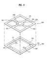
- FIG. 2 is an exploded perspective view illustrating a lead frame according to a first embodiment of the present invention;
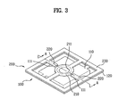
- FIG. 3 is a perspective view illustrating an assembled state of the lead frame shown in FIG. 2;
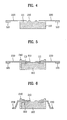
- FIG. 4 is a sectional view taken along the line A-A of FIG. 3;
- FIG. 5 is a sectional view illustrating a state in which a molded structure is provided at the lead frame shown in FIG. 4;
- FIG. 6 is a sectional view of the lead frame according to the first embodiment of the present invention;
- FIG. 7 is an exploded perspective view illustrating a lead frame according to a second embodiment of the present invention;
- FIG. 8 is a sectional view illustrating an assembled state of the lead frame shown in FIG. 7;
- FIG. 9 is a plan view illustrating an example of a second frame for forming a multi-chip structure on the lead frame according to the present invention;
- FIG. 10 is a sectional view taken along the line B-B of FIG. 9;
- FIG. 11 is a plan view illustrating an example of a first frame for forming a multi-chip structure on the lead frame according to the present invention;
- FIG. 12 is a sectional view illustrating an example of a light emitting device package according to the present invention;
- FIG. 13 is a plan view of the light emitting device package shown in FIG. 12; and
- FIG. 14 is a plan view illustrating another example of the light emitting device package according to the present invention.
- Reference will now be made in detail to the preferred embodiments of the present invention, examples of which are illustrated in the accompanying drawings.
- The present invention may, however, be embodied in many alternate forms and should not be construed as limited to the embodiments set forth herein. Accordingly, while the invention is susceptible to various modifications and alternative forms, specific embodiments thereof are shown by way of example in the drawings and will herein be described in detail. It should be understood, however, that there is no intent to limit the invention to the particular forms disclosed, but on the contrary, the invention is to cover all modifications, equivalents, and alternatives falling within the spirit and scope of the invention as defined by the claims
- The same reference numbers will be used throughout the drawings to refer to the same or like parts. In the drawings, dimensions of layers and regions are exaggerated for clarity of description.
- It will be understood that, when an element such as a layer, region or substrate is referred to as being "on" another element, it can be directly on the other element or intervening elements may also be present. It will also be understood that if part of an element, such as a surface, is referred to as "inner," it is farther to the outside of the device than other parts of the element.
- In addition, relative terms, such as "beneath" and "overlies", may be used herein to describe one layer's or region's relationship to another layer or region as illustrated in the figures.
- It will be understood that these terms are intended to encompass different orientations of the device in addition to the orientation depicted in the figures. Finally, the term "directly" means that there are no intervening elements. As used herein, the term "and/or" includes any and all combinations of one or more of the associated listed items.
- It will be understood that, although the terms first, second, etc. may be used herein to describe various elements, components, regions, layers and/or sections, these elements, components, regions, layers and/or sections should not be limited by these terms.
- The above terms first, second, etc. are used simply to discriminate any one element, component, region, layer, or area from other elements, components, regions, layers, or areas. Accordingly, the terms first region, first layer, first area, etc., which will be described hereinafter, may be replaced by the terms second region, second layer, or second area, etc.
- Hereinafter, the preferred embodiments of the present invention will be described in detail with reference to the accompanying drawings.
- As shown in FIG. 2, there are provided a
first frame 100 and asecond frame 200, which may be coupled to each other, so as to complete a lead frame, on which a light emitting device chip will be mounted. - Specifically, the
first frame 100 may include afirst rim 120, and aheat sink 110 located inside thefirst rim 120, theheat sink 110 being connected to thefirst rim 120 viafirst connectors 121. Thesecond frame 200 may include asecond rim 230, amount 210 located inside thesecond rim 230, themount 210 being connected to thesecond rim 230 viasecond connectors 231, and leads 220 extended from thesecond rim 230 toward themount 210. - In this case, the light emitting device chip is coupled to the
heat sink 110, so as to be operated by theheat sink 110. Theheat sink 110 is able to discharge heat generated during operation of the light emitting device chip, and in particular, may be made of a metal having a high thermal-conductivity. - The
mount 210 may be internally formed with ahole 211 for mounting the light emitting device chip. Themount 210 may have a circular shape and be inclined toward the center of thesecond frame 200. - The inclined portion of the
mount 210 may be formed with a film by use of a high-reflectivity material, such as a metal, to provide themount 210 with a reflective surface. - As shown in FIG. 2, the
mount 210 may be connected to thesecond rim 230 via twosecond connectors 231, and theheat sink 110 may be connected to thefirst rim 120 via twofirst connectors 121. - These
connectors rims - Meanwhile, to couple the
first frame 100 and thesecond frame 200 to each other, theheat sink 110 hasfirst recesses 111 formed at positions where theheat sink 110 is overlapped with theleads 220. This has the effect of preventing electrical short-circuit between theleads 220 and theheat sink 110. - FIG. 3 illustrates a coupled state of the first and
second frames - Also, FIG. 4 illustrates the cross section of the coupled first and
second frames - Referring to FIG. 5, a molded
structure 240 is formed through the coupled first andsecond frames second frames - In this case, the molded
structure 240 is formed by a transfer molding process or injection molding process. - After forming the molded
structure 240, the above mentionedconnectors rims leads 220 is bent, at its appropriate position not surrounded by the moldedstructure 240, to have a shape as shown in FIG. 6. - Here, the reason why bending the
leads 220 is to facilitate bonding of the light emitting device package to a substrate, such as a sub-mount substrate. - As shown in FIG. 6, a
space 300 is defined between theheat sink 110 and theleads 220. Specifically, thespace 300 may be defined by thefirst recesses 111 formed at theheat sink 110. - In an alternative embodiment, as shown in FIG. 7, instead of forming the
recesses 111 at theheat sink 110 in order to define thespace 300, asecond recess 221 may be formed at a part of a lower surface of each lead 220. Other configurations are identical to those shown in FIG. 2. - With the same procedure as described above with reference to FIGs. 3 to 5, a lead frame as shown in FIG. 8 can be accomplished by the configurations shown in FIG. 7.
- As shown, in the present embodiment, the
space 300 is defined, by thesecond recesses 221 formed at the lower surfaces of theleads 220, at positions where theheat sink 110 is overlapped with theleads 220. - As occasion demands, defining the
space 300 by forming thesecond recesses 221 at theleads 220 may be more advantageous than defining thespace 300 by forming thefirst recesses 111 at theheat sink 110. - This is because, when a plurality of light emitting device chips are coupled to the lead frame, namely, when forming a multi-chip package, the number of the
leads 220 have to be increased as many as the number of the chips, and consequently, thespace 300 for preventing electrical short-circuit have to be increased in proportion to the increased number of theleads 220. - Since the lower
first frame 100 including theheat sink 110 is made of a thick material, however, it may be difficult to pattern thefirst recesses 111 in thefirst frame 100 due to a relatively complex shape of the first recesses 111. - On the other hand, the upper
second frame 200 has a smaller thickness than that of the lowerfirst frame 100, and therefore, thespace 300 can be defined easily by forming thesecond recesses 221 at theleads 220 via an etching process or stamping process. - FIGs. 9 to 14 illustrate an embodiment in which the lead frame is used to construct a multi-chip package.
- As shown in FIG. 9, to construct a package including a plurality of light emitting device chips, plural pairs of
leads 220 may be provided. - In FIG. 9, more specifically, the
second frame 200 is provided with three pairs ofleads 220, for application of three light emitting device chips. - As shown in FIG. 10, each lead 220 may have the
second recess 221 formed at the lower surface thereof as described above, to define the space 300 (See FIG. 12). - Accordingly, all the
leads 220 have no risk of coming into contact with theheat sink 110, and thus, it is possible to prevent electrical short-circuit between theleads 220 and theheat sink 110. - The
mount 210 may be longitudinally formed with thehole 221, in consideration of a mounting space for the plurality of light emitting device chips. Thehole 221 may have a rectangular or elliptical shape. - The
mount 210 may be connected to thesecond rim 230 via thesecond connectors 231. - In the present embodiment, as shown in FIG. 11, the
first frame 110 includes theheat sink 110, and similarly, theheat sink 110 may be connected to thefirst rim 120 via thefirst connectors 121. - The first and
second frames - Specifically, the
mount 210 and theleads 220 are coupled onto theheat sink 110 by the moldedstructure 240, to thereby complete the lead frame. One or more light emittingdevice chips 400 are mounted on themount 210. - The light emitting
device chips 400 are attached to theheat sink 110 by use of a heat transfer material, and electrically connected to theleads 220 viawires 410. - Thereafter, a sealing
material 500 may be filled over the light emittingdevice chips 400, and in turn, alens 600 may be mounted over the sealingmaterial 500. - The sealing
material 500 may be selected from among a silicone sealing material and other resins including epoxy resin. - Meanwhile, as occasion demands, the sealing
material 500 may contain phosphor for changing colors of lights discharged from the light emitting device chips 400. - FIG. 13 illustrates a light emitting device package, which includes three light emitting
device chips 400 for emitting three colors of lights. Here, the three colors of lights may include red, green, and blue lights, and white color may be created by blending the three colors of lights. - Of course, it will be appreciated that other light emitting
device chips 400 for emitting other colors of lights may be used. - Meanwhile, as shown in FIG. 14, a light emitting device package may include four light emitting device chips 400. For example, in addition to the red, green, and blue light emitting device chips, the package may further include a light emitting device chip for emitting a supplementary color of light.
- Although FIG. 14 illustrates a state in which the four light emitting
device chips 400 and theleads 220 are radially arranged, it will be appreciated that they are arranged in a line as shown in FIG. 13. - In addition to the above mentioned four light emitting
device chips 400, if necessary, additional light emittingdevice chips 400 may be arranged together with theleads 200. - Of course, other light emitting device packages capable of emitting various colors of lights except for white light can be accomplished.
- Moreover, it will be appreciated that multiple light emitting device chips for emitting white light or other single color light may be provided to achieve an increase in brightness. Accordingly, the package having the increased brightness can be used as an illumination package or other decorative packages.
- It will be apparent to those skilled in the art that various modifications and variations can be made in the present invention without departing from the spirit or scope of the inventions. Thus, it is intended that the present invention covers the modifications and variations of this invention provided they come within the scope of the appended claims and their equivalents.
Claims (20)
- A light emitting device package comprising:a first frame including a heat sink;a second frame coupled to an upper side of the first frame, the second frame including at least one pair of leads and a mount formed with a hole; anda molded structure for coupling the first and second frames to each other.
- The light emitting device package according to claim 1, wherein a space is defined between the heat sink and the leads for providing a gap between the heat sink and the leads.
- The light emitting device package according to claim 2, wherein the space includes first recesses formed in the heat sink at positions where the heat sink is overlapped with the leads.
- The light emitting device package according to claim 2, wherein the space includes second recesses formed in the leads at positions where the leads are overlapped with the heat sink.
- The light emitting device package according to claim 2, wherein the molded structure is formed in the space.
- The light emitting device package according to claim 1, wherein the mount has a circular, rectangular, or elliptical shape.
- The light emitting device package according to claim 1, wherein the mount has an inwardly inclined portion.
- The light emitting device package according to claim 7, wherein the inclined portion has a reflective surface.
- The light emitting device package according to claim 1, wherein the leads comprise three or more pairs of leads.
- The light emitting device package according to claim 1, further comprising:at least one light emitting device chip located inside the mount.
- The light emitting device package according to claim 10, wherein the light emitting device chip is attached to the heat sink and electrically connected to the leads.
- The light emitting device package according to claim 11, wherein the light emitting device chip is connected to the leads via wires.
- The light emitting device package according to claim 1, wherein a plurality of light emitting device chips are mounted inside the mount.
- The light emitting device package according to claim 1, further comprising:a sealing material; anda lens,wherein the sealing material and the lens are provided over the mount in sequence.
- The light emitting device package according to claim 14, wherein the sealing material includes silicone or epoxy.
- A lead frame comprising:a first frame including a heat sink; anda second frame coupled to the first frame, the second frame including at least one pair of leads, and a mount formed with a hole.
- The lead frame according to claim 16, wherein the heat sink is connected to a first rim of the first frame, and the mount and the leads are connected to a second rim of the second frame.
- The lead frame according to claim 16, wherein the heat sink has a thickness larger than that of the leads.
- The lead frame according to claim 16, wherein a space is defined between the heat sink and the leads for providing a gap between the heat sink and the leads.
- A light emitting device package comprising:a heat sink;a frame coupled to the heat sink and including at least one pair of leads and a mount formed with a hole; anda molded structure for coupling the heat sink and the frame to each other.
Applications Claiming Priority (2)
| Application Number | Priority Date | Filing Date | Title |
|---|---|---|---|
| KR1020060010003A KR100809816B1 (en) | 2006-02-02 | 2006-02-02 | Lead frame, light emitting device package using same, and method for manufacturing same |
| KR1020060083014A KR100781285B1 (en) | 2006-08-30 | 2006-08-30 | Lead frame and light emitting device package for light emitting device |
Publications (3)
| Publication Number | Publication Date |
|---|---|
| EP1816688A2 true EP1816688A2 (en) | 2007-08-08 |
| EP1816688A3 EP1816688A3 (en) | 2014-06-18 |
| EP1816688B1 EP1816688B1 (en) | 2016-11-02 |
Family
ID=37903974
Family Applications (1)
| Application Number | Title | Priority Date | Filing Date |
|---|---|---|---|
| EP07290124.2A Active EP1816688B1 (en) | 2006-02-02 | 2007-01-31 | Light emitting diode package |
Country Status (4)
| Country | Link |
|---|---|
| US (1) | US7855391B2 (en) |
| EP (1) | EP1816688B1 (en) |
| JP (1) | JP5209881B2 (en) |
| CN (1) | CN102903707B (en) |
Cited By (4)
| Publication number | Priority date | Publication date | Assignee | Title |
|---|---|---|---|---|
| DE102008003971A1 (en) * | 2008-01-11 | 2009-07-16 | Ledon Lighting Jennersdorf Gmbh | Light-emitting diode arrangement with protective frame |
| EP2038924A4 (en) * | 2006-06-30 | 2011-03-23 | Seoul Semiconductor Co Ltd | MOUNTING FRAME PROVIDED WITH A HEAT SINK HOLDING ELEMENT, METHOD FOR MANUFACTURING THE LIGHT EMITTING DIODE HOUSING USING SUCH FRAME, AND LIGHT EMITTING DIODE HOUSING MADE ACCORDING TO THE ABOVE-MENTIONED METHOD |
| EP2469617A3 (en) * | 2010-12-22 | 2013-04-17 | PSI Technologies Inc. | Scalable heat dissipating microelectronic integration platform (SHDMIP) for lighting solutions and method of manufacturing thereof |
| EP2469614A3 (en) * | 2010-12-24 | 2014-07-30 | Samsung Electronics Co., Ltd. | Light emitting device package and method of manufacturing the same |
Families Citing this family (14)
| Publication number | Priority date | Publication date | Assignee | Title |
|---|---|---|---|---|
| CN101939852A (en) * | 2007-12-24 | 2011-01-05 | 三星Led株式会社 | LED Package |
| JP5416975B2 (en) * | 2008-03-11 | 2014-02-12 | ローム株式会社 | Semiconductor light emitting device |
| KR101660721B1 (en) * | 2009-06-15 | 2016-09-29 | 엘지전자 주식회사 | Light emitting diode package, and back-light unit and liquid crystal display device using the same |
| KR101628366B1 (en) * | 2009-07-06 | 2016-06-08 | 엘지전자 주식회사 | optical assembly, backlight unit having the same, and display apparatus thereof |
| EP2354817A1 (en) * | 2009-12-14 | 2011-08-10 | Lg Electronics Inc. | Backlight unit, and display apparatus including the backlight unit |
| KR101766719B1 (en) * | 2010-03-25 | 2017-08-09 | 엘지이노텍 주식회사 | Light emitting diode and Light emitting device comprising the same |
| JP2012049278A (en) * | 2010-08-26 | 2012-03-08 | I-Chiun Precision Industry Co Ltd | Method for manufacturing electrothermal separation type light-emitting diode bracket |
| US8575645B2 (en) * | 2011-11-22 | 2013-11-05 | GEM Weltronics TWN Corporation | Thin multi-layer LED array engine |
| WO2018071353A1 (en) | 2016-10-10 | 2018-04-19 | The Procter & Gamble Company | Personal care compositions substantially free of sulfated surfactants and containing a gel network |
| US11628126B2 (en) | 2018-06-05 | 2023-04-18 | The Procter & Gamble Company | Clear cleansing composition |
| TWI800538B (en) | 2018-10-08 | 2023-05-01 | 晶元光電股份有限公司 | Light-emitting device |
| CN114597188A (en) * | 2020-12-02 | 2022-06-07 | 新光电气工业株式会社 | Lead frame, semiconductor device, and manufacturing method of lead frame |
| US12053130B2 (en) | 2021-02-12 | 2024-08-06 | The Procter & Gamble Company | Container containing a shampoo composition with an aesthetic design formed by bubbles |
| US11633072B2 (en) | 2021-02-12 | 2023-04-25 | The Procter & Gamble Company | Multi-phase shampoo composition with an aesthetic design |
Family Cites Families (17)
| Publication number | Priority date | Publication date | Assignee | Title |
|---|---|---|---|---|
| EP0629507B1 (en) * | 1993-06-18 | 1997-12-03 | Xeikon Nv | Led recording head |
| JP3618534B2 (en) * | 1997-11-28 | 2005-02-09 | 同和鉱業株式会社 | Optical communication lamp device and manufacturing method thereof |
| US6335548B1 (en) * | 1999-03-15 | 2002-01-01 | Gentex Corporation | Semiconductor radiation emitter package |
| US6274924B1 (en) | 1998-11-05 | 2001-08-14 | Lumileds Lighting, U.S. Llc | Surface mountable LED package |
| DE19918370B4 (en) * | 1999-04-22 | 2006-06-08 | Osram Opto Semiconductors Gmbh | LED white light source with lens |
| US6517218B2 (en) * | 2000-03-31 | 2003-02-11 | Relume Corporation | LED integrated heat sink |
| JP3770192B2 (en) * | 2002-04-12 | 2006-04-26 | 松下電器産業株式会社 | Chip-type LED lead frame |
| WO2004001862A1 (en) * | 2002-06-19 | 2003-12-31 | Sanken Electric Co., Ltd. | Semiconductor light emitting device, method for producing the same and reflector for semiconductor light emitting device |
| JP3910171B2 (en) * | 2003-02-18 | 2007-04-25 | シャープ株式会社 | Semiconductor light emitting device, method for manufacturing the same, and electronic imaging device |
| WO2004102685A1 (en) | 2003-05-14 | 2004-11-25 | Nano Packaging Technology, Inc. | Light emitting device, package structure thereof and manufacturing method thereof |
| JP3938100B2 (en) * | 2003-05-15 | 2007-06-27 | 邦裕 服部 | LED lamp and LED lighting fixture |
| KR100575216B1 (en) | 2004-03-05 | 2006-04-28 | 럭스피아 주식회사 | Package base for light emitting device |
| KR100613065B1 (en) | 2004-05-21 | 2006-08-16 | 서울반도체 주식회사 | LED package using high thermal conductivity reflector and its manufacturing method |
| CN2710159Y (en) * | 2004-06-11 | 2005-07-13 | 佛山市国星光电科技有限公司 | Power LED mounting |
| EP1794808B1 (en) * | 2004-09-10 | 2017-08-09 | Seoul Semiconductor Co., Ltd. | Light emitting diode package having multiple molding resins |
| KR100635779B1 (en) | 2005-01-03 | 2006-10-17 | 서울반도체 주식회사 | Lead frame having heat sink support ring, light emitting diode package manufacturing method using same and light emitting diode package manufactured by same |
| WO2006065007A1 (en) * | 2004-12-16 | 2006-06-22 | Seoul Semiconductor Co., Ltd. | Leadframe having a heat sink supporting ring, fabricating method of a light emitting diodepackage using the same and light emitting diodepackage fabbricated by the method |
-
2007
- 2007-01-31 EP EP07290124.2A patent/EP1816688B1/en active Active
- 2007-02-01 JP JP2007022571A patent/JP5209881B2/en active Active
- 2007-02-02 CN CN201210326272.1A patent/CN102903707B/en active Active
- 2007-02-02 US US11/701,460 patent/US7855391B2/en active Active
Cited By (6)
| Publication number | Priority date | Publication date | Assignee | Title |
|---|---|---|---|---|
| EP2038924A4 (en) * | 2006-06-30 | 2011-03-23 | Seoul Semiconductor Co Ltd | MOUNTING FRAME PROVIDED WITH A HEAT SINK HOLDING ELEMENT, METHOD FOR MANUFACTURING THE LIGHT EMITTING DIODE HOUSING USING SUCH FRAME, AND LIGHT EMITTING DIODE HOUSING MADE ACCORDING TO THE ABOVE-MENTIONED METHOD |
| US8482023B2 (en) | 2006-06-30 | 2013-07-09 | Seoul Semiconductor Co., Ltd. | Leadframe having a heat sink supporting part, fabricating method of a light emitting diode package using the same, and light emitting diode package fabricated by the method |
| DE102008003971A1 (en) * | 2008-01-11 | 2009-07-16 | Ledon Lighting Jennersdorf Gmbh | Light-emitting diode arrangement with protective frame |
| EP2469617A3 (en) * | 2010-12-22 | 2013-04-17 | PSI Technologies Inc. | Scalable heat dissipating microelectronic integration platform (SHDMIP) for lighting solutions and method of manufacturing thereof |
| US8669580B2 (en) | 2010-12-22 | 2014-03-11 | Psi Technologies, Inc. | Scalable heat dissipating microelectronic integration platform (SHDMIP) for lighting solutions and method of manufacturing thereof |
| EP2469614A3 (en) * | 2010-12-24 | 2014-07-30 | Samsung Electronics Co., Ltd. | Light emitting device package and method of manufacturing the same |
Also Published As
| Publication number | Publication date |
|---|---|
| CN102903707A (en) | 2013-01-30 |
| US7855391B2 (en) | 2010-12-21 |
| EP1816688A3 (en) | 2014-06-18 |
| EP1816688B1 (en) | 2016-11-02 |
| JP2007208265A (en) | 2007-08-16 |
| JP5209881B2 (en) | 2013-06-12 |
| US20070210325A1 (en) | 2007-09-13 |
| CN102903707B (en) | 2015-09-30 |
Similar Documents
| Publication | Publication Date | Title |
|---|---|---|
| US7855391B2 (en) | Lead frame and light emitting device package using the same | |
| US8866166B2 (en) | Solid state lighting device | |
| US8564000B2 (en) | Light emitting devices for light emitting diodes (LEDs) | |
| KR101578090B1 (en) | Light emitting devices and methods | |
| US9231166B2 (en) | Light emitting device and lighting apparatus having the same | |
| US8097896B2 (en) | Light emitting device package and method for manufacturing the same | |
| CN109983590B (en) | Light emitting device package and light source unit | |
| TWI523273B (en) | Light-emitting diode package with contrast surface | |
| KR100550750B1 (en) | Light emitting diode package and manufacturing method thereof | |
| CN101427369A (en) | Lead frame having heat sink supporting part, method of manufacturing light emitting diode package using the same, and light emitting diode package manufactured by the method | |
| US20090294793A1 (en) | Led package and method of manufacturing the same | |
| TWI476963B (en) | LED package | |
| JP2006080251A (en) | Light emitting device and manufacturing method thereof | |
| CN103545431A (en) | Light emitting device | |
| CN101013735A (en) | Lead frame and light emitting device package using the same | |
| US20160254423A1 (en) | Non-magnified led for high center-beam candle power | |
| US20100213497A1 (en) | Light emitting device package and lighting system including the same | |
| KR101327124B1 (en) | Lighting Emitting Apparatus | |
| US20100148201A1 (en) | Led package | |
| CN202111155U (en) | LED package | |
| KR100781285B1 (en) | Lead frame and light emitting device package for light emitting device | |
| TW202612554A (en) | Lens structures for light-emitting diode (led) chips in led packages | |
| CN202797078U (en) | LED package and LED display |
Legal Events
| Date | Code | Title | Description |
|---|---|---|---|
| PUAI | Public reference made under article 153(3) epc to a published international application that has entered the european phase |
Free format text: ORIGINAL CODE: 0009012 |
|
| AK | Designated contracting states |
Kind code of ref document: A2 Designated state(s): AT BE BG CH CY CZ DE DK EE ES FI FR GB GR HU IE IS IT LI LT LU LV MC NL PL PT RO SE SI SK TR |
|
| AX | Request for extension of the european patent |
Extension state: AL BA HR MK YU |
|
| RAP1 | Party data changed (applicant data changed or rights of an application transferred) |
Owner name: LG INNOTEK CO., LTD. Owner name: LG ELECTRONICS INC. |
|
| 17P | Request for examination filed |
Effective date: 20140327 |
|
| RBV | Designated contracting states (corrected) |
Designated state(s): AT BE BG CH CY CZ DE DK EE ES FI FR GB GR HU IE IS IT LI LT LU LV MC NL PL PT RO SE SI SK TR |
|
| PUAL | Search report despatched |
Free format text: ORIGINAL CODE: 0009013 |
|
| RAP1 | Party data changed (applicant data changed or rights of an application transferred) |
Owner name: LG INNOTEK CO., LTD. Owner name: LG ELECTRONICS INC. |
|
| AK | Designated contracting states |
Kind code of ref document: A3 Designated state(s): AT BE BG CH CY CZ DE DK EE ES FI FR GB GR HU IE IS IT LI LT LU LV MC NL PL PT RO SE SI SK TR |
|
| AX | Request for extension of the european patent |
Extension state: AL BA HR MK RS |
|
| RIC1 | Information provided on ipc code assigned before grant |
Ipc: H01L 33/62 20100101AFI20140509BHEP Ipc: H01L 33/64 20100101ALI20140509BHEP |
|
| AKX | Designation fees paid |
Designated state(s): AT BE BG CH CY CZ DE DK EE ES FI FR GB GR HU IE IS IT LI LT LU LV MC NL PL PT RO SE SI SK TR |
|
| AXX | Extension fees paid |
Extension state: RS Extension state: HR Extension state: MK Extension state: BA Extension state: AL |
|
| REG | Reference to a national code |
Ref country code: DE Ref legal event code: R079 Ref document number: 602007048542 Country of ref document: DE Free format text: PREVIOUS MAIN CLASS: H01L0033000000 Ipc: H01L0033620000 |
|
| GRAP | Despatch of communication of intention to grant a patent |
Free format text: ORIGINAL CODE: EPIDOSNIGR1 |
|
| RIC1 | Information provided on ipc code assigned before grant |
Ipc: H01L 25/075 20060101ALN20160429BHEP Ipc: H01L 33/64 20100101ALI20160429BHEP Ipc: H01L 33/62 20100101AFI20160429BHEP |
|
| INTG | Intention to grant announced |
Effective date: 20160519 |
|
| RIN1 | Information on inventor provided before grant (corrected) |
Inventor name: PARK KWANG SUK Inventor name: WON YU HO |
|
| GRAS | Grant fee paid |
Free format text: ORIGINAL CODE: EPIDOSNIGR3 |
|
| GRAA | (expected) grant |
Free format text: ORIGINAL CODE: 0009210 |
|
| AK | Designated contracting states |
Kind code of ref document: B1 Designated state(s): AT BE BG CH CY CZ DE DK EE ES FI FR GB GR HU IE IS IT LI LT LU LV MC NL PL PT RO SE SI SK TR |
|
| REG | Reference to a national code |
Ref country code: GB Ref legal event code: FG4D |
|
| REG | Reference to a national code |
Ref country code: DE Ref legal event code: R081 Ref document number: 602007048542 Country of ref document: DE Owner name: SUZHOU LEKIN SEMICONDUCTOR CO. LTD., TAICANG, CN Free format text: FORMER OWNERS: LG ELECTRONICS INC., SEOUL, KR; LG INNOTEK CO., LTD., SEOUL/SOUL, KR Ref country code: DE Ref legal event code: R081 Ref document number: 602007048542 Country of ref document: DE Owner name: LG ELECTRONICS INC., KR Free format text: FORMER OWNERS: LG ELECTRONICS INC., SEOUL, KR; LG INNOTEK CO., LTD., SEOUL/SOUL, KR |
|
| REG | Reference to a national code |
Ref country code: AT Ref legal event code: REF Ref document number: 842632 Country of ref document: AT Kind code of ref document: T Effective date: 20161115 Ref country code: CH Ref legal event code: EP |
|
| REG | Reference to a national code |
Ref country code: IE Ref legal event code: FG4D |
|
| REG | Reference to a national code |
Ref country code: DE Ref legal event code: R096 Ref document number: 602007048542 Country of ref document: DE |
|
| REG | Reference to a national code |
Ref country code: FR Ref legal event code: PLFP Year of fee payment: 11 |
|
| PG25 | Lapsed in a contracting state [announced via postgrant information from national office to epo] |
Ref country code: LV Free format text: LAPSE BECAUSE OF FAILURE TO SUBMIT A TRANSLATION OF THE DESCRIPTION OR TO PAY THE FEE WITHIN THE PRESCRIBED TIME-LIMIT Effective date: 20161102 |
|
| REG | Reference to a national code |
Ref country code: NL Ref legal event code: MP Effective date: 20161102 |
|
| REG | Reference to a national code |
Ref country code: LT Ref legal event code: MG4D |
|
| REG | Reference to a national code |
Ref country code: AT Ref legal event code: MK05 Ref document number: 842632 Country of ref document: AT Kind code of ref document: T Effective date: 20161102 |
|
| PG25 | Lapsed in a contracting state [announced via postgrant information from national office to epo] |
Ref country code: GR Free format text: LAPSE BECAUSE OF FAILURE TO SUBMIT A TRANSLATION OF THE DESCRIPTION OR TO PAY THE FEE WITHIN THE PRESCRIBED TIME-LIMIT Effective date: 20170203 Ref country code: LT Free format text: LAPSE BECAUSE OF FAILURE TO SUBMIT A TRANSLATION OF THE DESCRIPTION OR TO PAY THE FEE WITHIN THE PRESCRIBED TIME-LIMIT Effective date: 20161102 Ref country code: SE Free format text: LAPSE BECAUSE OF FAILURE TO SUBMIT A TRANSLATION OF THE DESCRIPTION OR TO PAY THE FEE WITHIN THE PRESCRIBED TIME-LIMIT Effective date: 20161102 Ref country code: NL Free format text: LAPSE BECAUSE OF FAILURE TO SUBMIT A TRANSLATION OF THE DESCRIPTION OR TO PAY THE FEE WITHIN THE PRESCRIBED TIME-LIMIT Effective date: 20161102 |
|
| RAP2 | Party data changed (patent owner data changed or rights of a patent transferred) |
Owner name: LG ELECTRONICS INC. Owner name: LG INNOTEK CO., LTD. |
|
| PG25 | Lapsed in a contracting state [announced via postgrant information from national office to epo] |
Ref country code: PT Free format text: LAPSE BECAUSE OF FAILURE TO SUBMIT A TRANSLATION OF THE DESCRIPTION OR TO PAY THE FEE WITHIN THE PRESCRIBED TIME-LIMIT Effective date: 20170302 Ref country code: PL Free format text: LAPSE BECAUSE OF FAILURE TO SUBMIT A TRANSLATION OF THE DESCRIPTION OR TO PAY THE FEE WITHIN THE PRESCRIBED TIME-LIMIT Effective date: 20161102 Ref country code: AT Free format text: LAPSE BECAUSE OF FAILURE TO SUBMIT A TRANSLATION OF THE DESCRIPTION OR TO PAY THE FEE WITHIN THE PRESCRIBED TIME-LIMIT Effective date: 20161102 Ref country code: ES Free format text: LAPSE BECAUSE OF FAILURE TO SUBMIT A TRANSLATION OF THE DESCRIPTION OR TO PAY THE FEE WITHIN THE PRESCRIBED TIME-LIMIT Effective date: 20161102 Ref country code: IS Free format text: LAPSE BECAUSE OF FAILURE TO SUBMIT A TRANSLATION OF THE DESCRIPTION OR TO PAY THE FEE WITHIN THE PRESCRIBED TIME-LIMIT Effective date: 20170302 Ref country code: FI Free format text: LAPSE BECAUSE OF FAILURE TO SUBMIT A TRANSLATION OF THE DESCRIPTION OR TO PAY THE FEE WITHIN THE PRESCRIBED TIME-LIMIT Effective date: 20161102 Ref country code: BE Free format text: LAPSE BECAUSE OF NON-PAYMENT OF DUE FEES Effective date: 20170131 |
|
| PG25 | Lapsed in a contracting state [announced via postgrant information from national office to epo] |
Ref country code: RO Free format text: LAPSE BECAUSE OF FAILURE TO SUBMIT A TRANSLATION OF THE DESCRIPTION OR TO PAY THE FEE WITHIN THE PRESCRIBED TIME-LIMIT Effective date: 20161102 Ref country code: SK Free format text: LAPSE BECAUSE OF FAILURE TO SUBMIT A TRANSLATION OF THE DESCRIPTION OR TO PAY THE FEE WITHIN THE PRESCRIBED TIME-LIMIT Effective date: 20161102 Ref country code: CZ Free format text: LAPSE BECAUSE OF FAILURE TO SUBMIT A TRANSLATION OF THE DESCRIPTION OR TO PAY THE FEE WITHIN THE PRESCRIBED TIME-LIMIT Effective date: 20161102 Ref country code: EE Free format text: LAPSE BECAUSE OF FAILURE TO SUBMIT A TRANSLATION OF THE DESCRIPTION OR TO PAY THE FEE WITHIN THE PRESCRIBED TIME-LIMIT Effective date: 20161102 Ref country code: DK Free format text: LAPSE BECAUSE OF FAILURE TO SUBMIT A TRANSLATION OF THE DESCRIPTION OR TO PAY THE FEE WITHIN THE PRESCRIBED TIME-LIMIT Effective date: 20161102 |
|
| REG | Reference to a national code |
Ref country code: DE Ref legal event code: R097 Ref document number: 602007048542 Country of ref document: DE |
|
| PG25 | Lapsed in a contracting state [announced via postgrant information from national office to epo] |
Ref country code: IT Free format text: LAPSE BECAUSE OF FAILURE TO SUBMIT A TRANSLATION OF THE DESCRIPTION OR TO PAY THE FEE WITHIN THE PRESCRIBED TIME-LIMIT Effective date: 20161102 Ref country code: BE Free format text: LAPSE BECAUSE OF FAILURE TO SUBMIT A TRANSLATION OF THE DESCRIPTION OR TO PAY THE FEE WITHIN THE PRESCRIBED TIME-LIMIT Effective date: 20161102 Ref country code: BG Free format text: LAPSE BECAUSE OF FAILURE TO SUBMIT A TRANSLATION OF THE DESCRIPTION OR TO PAY THE FEE WITHIN THE PRESCRIBED TIME-LIMIT Effective date: 20170202 |
|
| REG | Reference to a national code |
Ref country code: CH Ref legal event code: PL |
|
| PLBE | No opposition filed within time limit |
Free format text: ORIGINAL CODE: 0009261 |
|
| STAA | Information on the status of an ep patent application or granted ep patent |
Free format text: STATUS: NO OPPOSITION FILED WITHIN TIME LIMIT |
|
| PG25 | Lapsed in a contracting state [announced via postgrant information from national office to epo] |
Ref country code: MC Free format text: LAPSE BECAUSE OF FAILURE TO SUBMIT A TRANSLATION OF THE DESCRIPTION OR TO PAY THE FEE WITHIN THE PRESCRIBED TIME-LIMIT Effective date: 20161102 |
|
| 26N | No opposition filed |
Effective date: 20170803 |
|
| PG25 | Lapsed in a contracting state [announced via postgrant information from national office to epo] |
Ref country code: CH Free format text: LAPSE BECAUSE OF NON-PAYMENT OF DUE FEES Effective date: 20170131 Ref country code: LI Free format text: LAPSE BECAUSE OF NON-PAYMENT OF DUE FEES Effective date: 20170131 |
|
| REG | Reference to a national code |
Ref country code: IE Ref legal event code: MM4A |
|
| PG25 | Lapsed in a contracting state [announced via postgrant information from national office to epo] |
Ref country code: SI Free format text: LAPSE BECAUSE OF FAILURE TO SUBMIT A TRANSLATION OF THE DESCRIPTION OR TO PAY THE FEE WITHIN THE PRESCRIBED TIME-LIMIT Effective date: 20161102 Ref country code: LU Free format text: LAPSE BECAUSE OF NON-PAYMENT OF DUE FEES Effective date: 20170131 |
|
| REG | Reference to a national code |
Ref country code: FR Ref legal event code: PLFP Year of fee payment: 12 |
|
| PG25 | Lapsed in a contracting state [announced via postgrant information from national office to epo] |
Ref country code: IE Free format text: LAPSE BECAUSE OF NON-PAYMENT OF DUE FEES Effective date: 20170131 |
|
| PG25 | Lapsed in a contracting state [announced via postgrant information from national office to epo] |
Ref country code: HU Free format text: LAPSE BECAUSE OF FAILURE TO SUBMIT A TRANSLATION OF THE DESCRIPTION OR TO PAY THE FEE WITHIN THE PRESCRIBED TIME-LIMIT; INVALID AB INITIO Effective date: 20070131 |
|
| PG25 | Lapsed in a contracting state [announced via postgrant information from national office to epo] |
Ref country code: CY Free format text: LAPSE BECAUSE OF NON-PAYMENT OF DUE FEES Effective date: 20161102 |
|
| PG25 | Lapsed in a contracting state [announced via postgrant information from national office to epo] |
Ref country code: TR Free format text: LAPSE BECAUSE OF FAILURE TO SUBMIT A TRANSLATION OF THE DESCRIPTION OR TO PAY THE FEE WITHIN THE PRESCRIBED TIME-LIMIT Effective date: 20161102 |
|
| REG | Reference to a national code |
Ref country code: DE Ref legal event code: R081 Ref document number: 602007048542 Country of ref document: DE Owner name: LG INNOTEK CO., LTD., KR Free format text: FORMER OWNERS: LG ELECTRONICS INC., SEOUL, KR; LG INNOTEK CO., LTD., SEOUL, KR Ref country code: DE Ref legal event code: R081 Ref document number: 602007048542 Country of ref document: DE Owner name: SUZHOU LEKIN SEMICONDUCTOR CO. LTD., TAICANG, CN Free format text: FORMER OWNERS: LG ELECTRONICS INC., SEOUL, KR; LG INNOTEK CO., LTD., SEOUL, KR Ref country code: DE Ref legal event code: R081 Ref document number: 602007048542 Country of ref document: DE Owner name: LG ELECTRONICS INC., KR Free format text: FORMER OWNERS: LG ELECTRONICS INC., SEOUL, KR; LG INNOTEK CO., LTD., SEOUL, KR |
|
| PGFP | Annual fee paid to national office [announced via postgrant information from national office to epo] |
Ref country code: GB Payment date: 20221220 Year of fee payment: 17 Ref country code: FR Payment date: 20221220 Year of fee payment: 17 |
|
| REG | Reference to a national code |
Ref country code: DE Ref legal event code: R081 Ref document number: 602007048542 Country of ref document: DE Owner name: LG INNOTEK CO., LTD., KR Free format text: FORMER OWNERS: LG ELECTRONICS INC., SEOUL, KR; SUZHOU LEKIN SEMICONDUCTOR CO. LTD., TAICANG, SUZHOU, CN Ref country code: DE Ref legal event code: R081 Ref document number: 602007048542 Country of ref document: DE Owner name: LG ELECTRONICS INC., KR Free format text: FORMER OWNERS: LG ELECTRONICS INC., SEOUL, KR; SUZHOU LEKIN SEMICONDUCTOR CO. LTD., TAICANG, SUZHOU, CN |
|
| GBPC | Gb: european patent ceased through non-payment of renewal fee |
Effective date: 20240131 |
|
| PG25 | Lapsed in a contracting state [announced via postgrant information from national office to epo] |
Ref country code: GB Free format text: LAPSE BECAUSE OF NON-PAYMENT OF DUE FEES Effective date: 20240131 |
|
| PG25 | Lapsed in a contracting state [announced via postgrant information from national office to epo] |
Ref country code: FR Free format text: LAPSE BECAUSE OF NON-PAYMENT OF DUE FEES Effective date: 20240131 |
|
| PG25 | Lapsed in a contracting state [announced via postgrant information from national office to epo] |
Ref country code: GB Free format text: LAPSE BECAUSE OF NON-PAYMENT OF DUE FEES Effective date: 20240131 Ref country code: FR Free format text: LAPSE BECAUSE OF NON-PAYMENT OF DUE FEES Effective date: 20240131 |
|
| REG | Reference to a national code |
Ref country code: DE Ref legal event code: R079 Ref document number: 602007048542 Country of ref document: DE Free format text: PREVIOUS MAIN CLASS: H01L0033620000 Ipc: H10H0020857000 |
|
| PGFP | Annual fee paid to national office [announced via postgrant information from national office to epo] |
Ref country code: DE Payment date: 20241223 Year of fee payment: 19 |