EP1815989A1 - Inkjet printhead employing piezoelectric actuator - Google Patents
Inkjet printhead employing piezoelectric actuator Download PDFInfo
- Publication number
- EP1815989A1 EP1815989A1 EP06252594A EP06252594A EP1815989A1 EP 1815989 A1 EP1815989 A1 EP 1815989A1 EP 06252594 A EP06252594 A EP 06252594A EP 06252594 A EP06252594 A EP 06252594A EP 1815989 A1 EP1815989 A1 EP 1815989A1
- Authority
- EP
- European Patent Office
- Prior art keywords
- piezoelectric
- inkjet printhead
- piezoelectric actuator
- layer
- damping layer
- Prior art date
- Legal status (The legal status is an assumption and is not a legal conclusion. Google has not performed a legal analysis and makes no representation as to the accuracy of the status listed.)
- Granted
Links
Images


Classifications
-
- B—PERFORMING OPERATIONS; TRANSPORTING
- B41—PRINTING; LINING MACHINES; TYPEWRITERS; STAMPS
- B41J—TYPEWRITERS; SELECTIVE PRINTING MECHANISMS, i.e. MECHANISMS PRINTING OTHERWISE THAN FROM A FORME; CORRECTION OF TYPOGRAPHICAL ERRORS
- B41J2/00—Typewriters or selective printing mechanisms characterised by the printing or marking process for which they are designed
- B41J2/005—Typewriters or selective printing mechanisms characterised by the printing or marking process for which they are designed characterised by bringing liquid or particles selectively into contact with a printing material
- B41J2/01—Ink jet
- B41J2/015—Ink jet characterised by the jet generation process
- B41J2/04—Ink jet characterised by the jet generation process generating single droplets or particles on demand
- B41J2/045—Ink jet characterised by the jet generation process generating single droplets or particles on demand by pressure, e.g. electromechanical transducers
- B41J2/055—Devices for absorbing or preventing back-pressure
-
- B—PERFORMING OPERATIONS; TRANSPORTING
- B41—PRINTING; LINING MACHINES; TYPEWRITERS; STAMPS
- B41J—TYPEWRITERS; SELECTIVE PRINTING MECHANISMS, i.e. MECHANISMS PRINTING OTHERWISE THAN FROM A FORME; CORRECTION OF TYPOGRAPHICAL ERRORS
- B41J2/00—Typewriters or selective printing mechanisms characterised by the printing or marking process for which they are designed
- B41J2/005—Typewriters or selective printing mechanisms characterised by the printing or marking process for which they are designed characterised by bringing liquid or particles selectively into contact with a printing material
- B41J2/01—Ink jet
- B41J2/015—Ink jet characterised by the jet generation process
- B41J2/04—Ink jet characterised by the jet generation process generating single droplets or particles on demand
- B41J2/045—Ink jet characterised by the jet generation process generating single droplets or particles on demand by pressure, e.g. electromechanical transducers
-
- B—PERFORMING OPERATIONS; TRANSPORTING
- B41—PRINTING; LINING MACHINES; TYPEWRITERS; STAMPS
- B41J—TYPEWRITERS; SELECTIVE PRINTING MECHANISMS, i.e. MECHANISMS PRINTING OTHERWISE THAN FROM A FORME; CORRECTION OF TYPOGRAPHICAL ERRORS
- B41J2/00—Typewriters or selective printing mechanisms characterised by the printing or marking process for which they are designed
- B41J2/005—Typewriters or selective printing mechanisms characterised by the printing or marking process for which they are designed characterised by bringing liquid or particles selectively into contact with a printing material
- B41J2/01—Ink jet
-
- B—PERFORMING OPERATIONS; TRANSPORTING
- B41—PRINTING; LINING MACHINES; TYPEWRITERS; STAMPS
- B41J—TYPEWRITERS; SELECTIVE PRINTING MECHANISMS, i.e. MECHANISMS PRINTING OTHERWISE THAN FROM A FORME; CORRECTION OF TYPOGRAPHICAL ERRORS
- B41J2/00—Typewriters or selective printing mechanisms characterised by the printing or marking process for which they are designed
- B41J2/005—Typewriters or selective printing mechanisms characterised by the printing or marking process for which they are designed characterised by bringing liquid or particles selectively into contact with a printing material
- B41J2/01—Ink jet
- B41J2/135—Nozzles
- B41J2/14—Structure thereof only for on-demand ink jet heads
- B41J2/14201—Structure of print heads with piezoelectric elements
- B41J2/14233—Structure of print heads with piezoelectric elements of film type, deformed by bending and disposed on a diaphragm
Definitions
- the present invention relates to an inkjet printhead, and more particularly, to an inkjet printhead which ejects ink in a piezoelectric method.
- an inkjet printhead prints a predetermined color image by ejecting fine droplets of printing ink to a desired position on a print paper.
- the inkjet printhead can be classified into two types according to an ink ejection method: a thermal inkjet printhead and a piezoelectric inkjet printhead.
- the thermal inkjet printhead generates a bubble in the ink using a heat source to eject the ink using an extension force of the bubble.
- the piezoelectric inkjet printhead uses a piezoelectric material to eject the ink using a pressure applied to the ink which is generated by the deformation of a piezoelectric material.
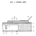
- FIG. 1 is a cross-sectional view showing the configuration of a conventional piezoelectric inkjet printhead.
- a fluid path forming substrate 10 includes a manifold 13 forming a path for ink, a plurality of restrictors 12, and a plurality of pressure chambers 11.
- a nozzle substrate 20 includes a plurality of nozzles 22 respectively corresponding to the pressure chambers 11.
- a piezoelectric actuator 40 is provided in the upper portion of the fluid path forming substrate 10.
- the manifold 13 is a path through which ink supplied from an ink reservoir is provided to each of the pressure chambers 11.
- the restrictor 12 is a path through which the ink passes from the manifold 13 into each of the pressure chamber 11.
- the pressure chambers 11 are filled with the ink to be ejected and arranged at one side or both sides of the manifold 13.
- the pressure chambers 11 generate a change in pressure for ejection or sucking of the ink as its volume varies according to the operation of the piezoelectric actuator 40.
- a portion forming the upper wall of the pressure chambers 11 of the fluid path forming substrate 10 functions as a vibration plate 14 which is deformed by the piezoelectric actuator 40.
- the piezoelectric actuator 40 includes a lower electrode 41, a piezoelectric layer 42, and an upper electrode 43 which are sequentially deposited on the fluid path forming substrate 10.
- a silicon oxide layer 31 is formed between the lower electrode 41 and the fluid path forming substrate 10 as an insulating layer.
- the lower electrode 41 is formed over the entire surface of the silicon oxide layer 31 to function as a common electrode.
- the piezoelectric layer 42 is formed on the lower electrode 41 to be located on the pressure chambers 11.
- the upper electrode 43 is formed on the piezoelectric layer 42 and functions as a drive electrode to apply a voltage to the piezoelectric layer 42.
- a flexible printed circuit 50 for supplying a voltage is connected to the upper electrode 43.
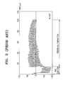
- FIG. 2 shows the result of measurement of the displacement of the piezoelectric layer 42, using a laser-dopler velocimetry (LDV), after a drive pulse is applied to the upper electrode 43.
- LDV laser-dopler velocimetry
- a piezoelectric inkjet printhead comprises a fluid path forming substrate having a pressure chamber, a piezoelectric actuator formed on the fluid path forming substrate and providing to the pressure chamber a drive force to eject ink, and a damping layer formed on at least the piezoelectric actuator and damping a residual vibration of the piezoelectric actuator.
- the damping layer may be formed to an area of an upper portion of the fluid path forming substrate corresponding to the pressure chamber.
- the piezoelectric inkjet printhead may further comprise a printed circuit to apply a drive voltage to drive the piezoelectric actuator, wherein the damping layer is formed on a conjunction portion between the printed circuit and the piezoelectric actuator.
- a mechanical loss rate of the damping layer may be larger than that of the piezoelectric actuator and that of the fluid path forming substrate.
- Young's modulus of the damping layer is not more than 5,000 MPa.
- the damping layer may be formed of one selected from a group consisting of silicon rubber, epoxy, polyurethane, and photoresist substance, or a combination thereof.
- a piezoelectric inkjet printhead comprising: a fluid path forming substrate having a pressure chamber; a piezoelectric actuator providing to the pressure chamber a drive force to eject ink; and a damping layer formed on the piezoelectric actuator, a mechanical loss rate of the damping layer is larger than that of the piezoelectric actuator and that of the fluid path forming substrate.
- the present invention thus provides a piezoelectric inkjet printhead which can quickly damp out the residual vibration of a piezoelectric layer.
- FIG. 3 is a cross-sectional view showing the configuration of an inkjet printhead according to an embodiment of the present invention.
- FIG. 4 is a plan view of the inkjet printhead of FIG. 3.
- an inkjet printhead according to an embodiment of the present invention includes a fluid path forming substrate 110 where an ink path is formed and a piezoelectric actuator 140 to provide an ink ejection pressure.
- the fluid path forming substrate 110 includes a pressure chamber 111, a manifold 113 to supply ink into the pressure chamber 111, and a restrictor 112.
- a nozzle 122 to eject the ink from the ink chamber 111 is formed in a nozzle substrate 120 which is attached to the fluid path forming substrate 110.
- a vibration plate 114 is provided on the pressure chamber 111 and deformed by the operation of the piezoelectric actuator 140.
- the ink path is defined by the fluid path forming substrate 110 and the nozzle substrate 120.
- the piezoelectric actuator 140 is formed on the fluid path forming substrate 110 and provides a drive force for ejecting the ink to the pressure chamber 111.
- the piezoelectric actuator 140 includes a lower electrode 141 to function as a common electrode, a piezoelectric layer 142 deformed by the application of a voltage, and an upper electrode 143 to function as a drive electrode.
- the lower electrode 141, the piezoelectric layer 142, and the upper electrode 143 are sequentially deposited on the fluid path forming substrate 110.
- the lower electrode 141 is formed on the fluid path forming substrate 110 where the pressure chamber 111 is formed.
- a silicon oxide layer 131 can be formed between the fluid path forming substrate 110 and the lower electrode 141 as an insulating layer.
- the lower electrode 141 is formed of a conductive metal material.
- the lower electrode 141 can be made into a single metal layer, or preferably two metal layers formed of a Ti layer and a Pt layer.
- the lower electrode 141 made of Ti/Pt layers not only functions as the common electrode but also as a diffusion barrier layer to prevent inter-diffusion between the piezoelectric layer 142 and the fluid path forming substrate 110 which are respectively formed on and below the lower electrode 141.
- the piezoelectric layer 142 is formed on the lower electrode 141 and is arranged at a position corresponding to the pressure chamber 111.
- the piezoelectric layer 142 can be formed of a piezoelectric material, preferably a PZT (lead zirconate titanate) ceramic material.
- the upper electrode 143 functions as the drive electrode to apply a voltage to the piezoelectric layer 142.
- the structures of the fluid path forming substrate 110, the nozzle substrate 120, and the piezoelectric actuator 140 shown in FIGS. 3 and 4 are merely an example. That is, an ink path having a variety of structures can be provided in the piezoelectric inkjet printhead and such an ink path can be formed using a plurality of substrates more than the two substrates 110 and 120 shown in FIG. 3. Also, the structure of the piezoelectric actuator 140 and the structure for connecting the piezoelectric actuator 140 and the voltage application drive circuit can be modified in a variety of ways.
- the present invention has a characteristic feature in the structure for damping a residual vibration of the piezoelectric layer 142, not in the structures of the ink path, the piezoelectric actuator 140, and the connection for the piezoelectric actuator 140 and the voltage application drive circuit.
- the vibration of the piezoelectric layer 142 needs to be quickly damped out.
- an active damping method, a passive damping method, and a method using a bulk actuator can be taken into consideration.
- the active damping method is to forcibly damp out a residual vibration by applying an auxiliary pulse next to a main drive pulse to eject ink to generate in the piezoelectric layer 142 a vibration opposite to a residual vibration wave of the piezoelectric layer 142.
- the auxiliary pulse is applied in a section between 15 ⁇ s and 100 ⁇ s in the graph of FIG. 2. According to this method, although quicker damping is possible, the structure of the drive circuit to drive the piezoelectric actuator 140 is complicated. Also, a time point to apply the auxiliary pulse needs to be carefully reviewed.
- the passive damping method is to add a material having a large mechanical loss rate to a vibrating material so that a passive damping material absorbs or consumes residual vibration energy.
- the bulk actuator refers to a piezoelectric actuator manufactured by etching a sintered piezoelectric material. Since the density of a material is high and the thickness thereof is large, stiffness is great. Thus, the bulk actuator is effective in damping the residual vibration. However, a manufacturing process of the bulk actuator is complicated and yield is low. Also, since the displacement of the bulk actuator is relatively small, a high drive voltage is required.
- a damping layer 160 is formed on the piezoelectric actuator 140. It is preferable that the mechanical loss rate of the damping layer 160 is greater than that of the piezoelectric actuator 140 or the fluid path forming substrate 110.
- the mechanical loss rate can be expressed in a variety of methods such as Young's modulus and a loss coefficient in a shear mode where the loss coefficient is a tangent value of an imaginary number portion/a real number portion of shear modulus "G".
- the mechanical loss rate is indicated by the Young's modulus. As the Young's modulus decreases, the mechanical loss rate increases.
- the Young's modulus of a silicon mono-crystalline substrate which can be used as the fluid path forming substrate 110 is about 150-2,000 GPa.
- the PZT (lead zirconate titanate) forming the piezoelectric layer 142 has a Young's modulus of about 40-600 GPa.
- the damping layer 160 must be so soft not to restrict a very small force and displacement generated by the piezoelectric actuator 140 to eject ink.
- the Young's modulus of the damping layer 160 needs to be sufficiently less than that of the fluid path forming substrate 110 or the piezoelectric layer 142.
- the Young's modulus of a material that can be employed as the damping layer 160 is preferably not more than about 5,000 MPa.
- the damping layer 160 can be formed of, for example, silicon rubber, preferably, any of RTV (room temperature volcanizing) silicon rubber, epoxy, polyurethane, and a photoresist material or a combination of one or two of them.
- RTV room temperature volcanizing
- the above-described materials are mere examples and the damping layer 160 can be formed of a variety of materials having a Young's modules that is sufficiently lower than that of the fluid path forming substrate 110 or the piezoelectric layer 142.
- the damping layer 160 is preferably formed to cover at least the upper portion of the piezoelectric actuator 140. More preferably, the damping layer 160 is formed to cover the overall area of the fluid path forming substrate 110 corresponding to the pressure chamber 111. Also, the damping layer 160 can be formed to cover a conjunction portion 152 between the flexible printed circuit 150 and the piezoelectric actuator 140. When the damping layer 160 is formed by using a dispenser or by spin coating or spray coating, it is formed over the overall upper portion of the print head including the piezoelectric actuator 140.
- FIG. 5 shows the result of the test of a damping effect after the damping layer 160 formed of silicon rubber is formed.
- the thickness of the damping layer 160 is about 2 mm and an average elastic coefficient of the silicon rubber is about 5 MPa.
- the voltage of a drive pulse applied to the piezoelectric actuator 140 is 35 V and the application time is 10 ⁇ s.
- the residual vibration is almost damped out within a period of about 35 ⁇ s after a drive pulse is applied. Compared to the result shown in FIG. 2, it is noted that the damping time of the residual vibration is remarkably reduced.
- the thickness of the damping layer 160 is set to 2 mm in the test, the present invention is not limited thereto.
- the displacement of the piezoelectric layer 142 is substantially proportional to the size of the piezoelectric layer 142. Since the displacement of the piezoelectric layer 142 decreases when the thickness of the piezoelectric layer 142 increases, a large drive voltage is needed to obtain the same displacement.
- the length of the piezoelectric layer 142 is dependent upon the length of the pressure chamber 111. Thus, to increase the size of the piezoelectric layer 142, the width of the piezoelectric layer 142 needs to be increased.
- the inkjet printhead capable of stably ejecting ink having a high viscosity can be provided.
- the drive circuit can be simplified and the frequency of the drive pulse can be increased.
- an inkjet printhead capable of stable and high speed operation can be provided.
- an ejection response characteristic with respect to the drive pulse can be improved. Movement stability of ink droplets can be secured so that high quality printing can be obtained.
- cross-talk between the adjacent pressure chambers 111 is lowered, the speed or volume of the ink droplets ejected from the nozzles can be uniformly maintained, thereby producing a uniform print quality.
- the damping layer 160 is formed to an area corresponding to the pressure chamber 111 of the fluid path forming substrate 110, a vibration transmitted to the entire fluid path forming substrate 110 by a pressure wave in the pressure chamber 111 can be absorbed. Additionally, the damping layer 160 can have a sealing function. When the number of ink ejection is accumulated, since the vibration plate 114 repeats vibrations, there is a possibility of generating micro-damage(for example cracks) in a corner portion 116 around a partition wall 115 extending to the restrictor 112. When the ink leaks through the cracks, the upper and lower electrodes 143 and 141 are short-circuited so that the jetting reliability may be seriously decreased.
- the damping layer 160 is formed to the area corresponding to the pressure chamber 111 of the fluid path forming substrate 110, the leakage of ink can be prevented. Also, the damping layer 160 can function as an electric, mechanical, and chemical surface protection layer of the entire inkjet printhead including the piezoelectric actuator 140. To maximize the effects of the sealing and surface protection functions, the damping layer 160 is more preferably forming over the entire upper surface of the fluid path forming substrate 110 including the piezoelectric actuator 140. Also, since the damping layer 160 is formed to cover the conjunction portion 152 between the flexible printed circuit 150 and the piezoelectric actuator 140, durability in combination of the flexible printed circuit 150 and the piezoelectric actuator 140 can be improved.
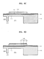
- FIGS. 6A through 6D are cross-sectional views showing a method for manufacturing the piezoelectric inkjet printhead of FIG. 3.
- the fluid path forming substrate 110 is prepared in which the pressure chamber 111, the restrictor 112, the manifold 113, and the vibration plate 114 are formed.
- the silicon oxide layer 131 is formed as an insulating layer on the upper surface of the fluid path forming substrate 110.
- the lower electrode 141 is formed on the silicon oxide layer 131.
- the lower electrode 141 can be formed of two metal layers of the Ti layer and the Pt layer as described above.
- the lower electrode 141 can be formed to have a predetermined thickness by depositing Ti and Pt on the entire surface of the silicon oxide layer 131 by deposition method.
- the piezoelectric layer 142 is formed by coating a piezoelectric material on the lower electrode 141 to have a predetermined thickness by patterning method, for example screen printing.
- the piezoelectric layer 142 is formed at a position corresponding to the pressure chamber 111.
- a PZT (lead zircornate titanate) ceramic material can be preferably used.
- FIG. 6D shows a state in which the upper electrode 143 is formed on the piezoelectric layer 142.
- the upper electrode 143 can be formed by screen printing a conductive metal material on the piezoelectric layer 142. After the piezoelectric layer 142 and the upper electrode 143 are sintered at a predetermined temperature, an electric field is applied to the piezoelectric layer 142 to perform a poling process which generates a piezoelectric characteristic.
- a damping material such as silicon rubber or epoxy is coated on the upper portion of the piezoelectric actuator 140 using a dispenser or by spin coating or spray coating, to form the damping layer 160.
- the damping layer 160 is not formed on a position where the wiring 151 of the flexible printed circuit 150 is bonded.
- the voltage application drive circuit for example, the wiring 151 of the flexible printed circuit 150, is bonded to the upper surface of the upper electrode 143 so that the piezoelectric inkjet printhead having the damping layer 160 as shown in FIG. 3 is manufactured.
- the damping layer 160 can be formed in the above-described method after the wiring 151 of the flexible printed circuit 150 is bonded to the upper electrode 142. In this case, the damping layer 160 is preferably formed to the conjunction portion 152. Although it is not shown in the drawing, the damping layer 160 can be formed by coating a damping material such as silicon rubber or epoxy on a surface exposed after the inkjet printhead is packaged to a bezel (not shown) using a dispenser or by spin coating or spray coating.
- a damping material such as silicon rubber or epoxy
- the piezoelectric inkjet printhead since the damping layer is formed on the upper portion of the piezoelectric actuator, the time to damp a residual vibration can be remarkably reduced. Thus, even when ink having a high viscosity is used, an inkjet printhead can stably eject ink. Also, the frequency of a drive pulse for driving the piezoelectric actuator can be increased so that an inkjet printhead capable of a stable and high speed operation can be provided. Since an ejection response characteristic with respect to the drive pulse can be improved and the movement stability of the ink droplet can be secured, high quality printing can be obtained and cross-talk between the adjacent pressure chambers can be reduced. Additionally, an effect of sealing for preventing leakage of ink and an effect of firmly maintaining the combination between the piezoelectric actuator and the flexible printed circuit can be obtained.
Landscapes
- Particle Formation And Scattering Control In Inkjet Printers (AREA)
Abstract
Description
- The present invention relates to an inkjet printhead, and more particularly, to an inkjet printhead which ejects ink in a piezoelectric method.
- In general, an inkjet printhead prints a predetermined color image by ejecting fine droplets of printing ink to a desired position on a print paper. The inkjet printhead can be classified into two types according to an ink ejection method: a thermal inkjet printhead and a piezoelectric inkjet printhead. The thermal inkjet printhead generates a bubble in the ink using a heat source to eject the ink using an extension force of the bubble. The piezoelectric inkjet printhead uses a piezoelectric material to eject the ink using a pressure applied to the ink which is generated by the deformation of a piezoelectric material.
- FIG. 1 is a cross-sectional view showing the configuration of a conventional piezoelectric inkjet printhead. Referring to FIG. 1, a fluid
path forming substrate 10 includes amanifold 13 forming a path for ink, a plurality ofrestrictors 12, and a plurality ofpressure chambers 11. Anozzle substrate 20 includes a plurality ofnozzles 22 respectively corresponding to thepressure chambers 11. Apiezoelectric actuator 40 is provided in the upper portion of the fluidpath forming substrate 10. Themanifold 13 is a path through which ink supplied from an ink reservoir is provided to each of thepressure chambers 11. Therestrictor 12 is a path through which the ink passes from themanifold 13 into each of thepressure chamber 11. Thepressure chambers 11 are filled with the ink to be ejected and arranged at one side or both sides of themanifold 13. Thepressure chambers 11 generate a change in pressure for ejection or sucking of the ink as its volume varies according to the operation of thepiezoelectric actuator 40. To this end, a portion forming the upper wall of thepressure chambers 11 of the fluidpath forming substrate 10 functions as avibration plate 14 which is deformed by thepiezoelectric actuator 40. - The
piezoelectric actuator 40 includes alower electrode 41, apiezoelectric layer 42, and anupper electrode 43 which are sequentially deposited on the fluidpath forming substrate 10. Asilicon oxide layer 31 is formed between thelower electrode 41 and the fluidpath forming substrate 10 as an insulating layer. Thelower electrode 41 is formed over the entire surface of thesilicon oxide layer 31 to function as a common electrode. Thepiezoelectric layer 42 is formed on thelower electrode 41 to be located on thepressure chambers 11. Theupper electrode 43 is formed on thepiezoelectric layer 42 and functions as a drive electrode to apply a voltage to thepiezoelectric layer 42. A flexible printedcircuit 50 for supplying a voltage is connected to theupper electrode 43. - When a drive pulse is applied to the
upper electrode 43, thepiezoelectric layer 42 is deformed and thevibration plate 14 is deformed so that the volume of each of thepressure chambers 11 is changed. Thus, the ink in thepressure chambers 11 is ejected through thenozzles 22. The frequency of the drive pulse is affected by the damping performance of thepiezoelectric layer 42. Therefore, the vibration of thepiezoelectric layer 42 needs to be quickly damped out. - FIG. 2 shows the result of measurement of the displacement of the
piezoelectric layer 42, using a laser-dopler velocimetry (LDV), after a drive pulse is applied to theupper electrode 43. Referring to FIG. 2, the displacement of thepiezoelectric layer 42 to eject the ink is generated for about 15 µs and then a residual vibration of thepiezoelectric layer 42 continues for about 85 µs. According to the result of the above test, when the frequency of the drive pulse is greater than 10 KHz, the displacement of thepiezoelectric layer 42 is affected by the residual vibration caused by the drive pulse of the preceding cycle. As a result, it is difficult to eject ink droplets at a constant speed and the volume of the ejected ink droplet may be irregular. Also, since a pressure wave in each of thepressure chambers 11 is not removed within a short time, cross-talk can be generated between theadjacent pressure chambers 11. - According to an aspect of the present invention, a piezoelectric inkjet printhead comprises a fluid path forming substrate having a pressure chamber, a piezoelectric actuator formed on the fluid path forming substrate and providing to the pressure chamber a drive force to eject ink, and a damping layer formed on at least the piezoelectric actuator and damping a residual vibration of the piezoelectric actuator.
- The damping layer may be formed to an area of an upper portion of the fluid path forming substrate corresponding to the pressure chamber.
- The piezoelectric inkjet printhead may further comprise a printed circuit to apply a drive voltage to drive the piezoelectric actuator, wherein the damping layer is formed on a conjunction portion between the printed circuit and the piezoelectric actuator.
- A mechanical loss rate of the damping layer may be larger than that of the piezoelectric actuator and that of the fluid path forming substrate. In one embodiment, Young's modulus of the damping layer is not more than 5,000 MPa.
- The damping layer may be formed of one selected from a group consisting of silicon rubber, epoxy, polyurethane, and photoresist substance, or a combination thereof.
- According to another aspect of the present invention, a piezoelectric inkjet printhead comprising: a fluid path forming substrate having a pressure chamber;
a piezoelectric actuator providing to the pressure chamber a drive force to eject ink; and a damping layer formed on the piezoelectric actuator, a mechanical loss rate of the damping layer is larger than that of the piezoelectric actuator and that of the fluid path forming substrate. - The present invention thus provides a piezoelectric inkjet printhead which can quickly damp out the residual vibration of a piezoelectric layer.
- The above and other features and advantages of the present invention will become more apparent by describing in detail preferred embodiments thereof with reference to the attached drawings in which:
- FIG. 1 is a cross-sectional view showing the configuration of a conventional piezoelectric inkjet printhead;
- FIG. 2 is a graph showing the residual vibration the piezoelectric layer;
- FIG. 3 is a cross-sectional view showing the configuration of an inkjet printhead according to an embodiment of the present invention;
- FIG. 4 is a plan view of the inkjet printhead of FIG. 3;
- FIG. 5 is a graph showing the damping effect of the residual vibration by the inkjet printhead of FIG. 3; and
- FIGS. 6A through 6D are cross-sectional views showing a method for manufacturing the inkjet printhead of FIG. 3.
- In the accompanying drawings, the same reference numerals indicate the same constituent elements. The size of each constituent element in the drawings can be exaggerated for the convenience of explanation. Also, when a layer is described to exist on another layer, the layer can exist while directly contacting the other layer or a third layer can exist therebetween. An embodiment of the present invention will be described in detail with reference to the accompanying drawings.
- FIG. 3 is a cross-sectional view showing the configuration of an inkjet printhead according to an embodiment of the present invention. FIG. 4 is a plan view of the inkjet printhead of FIG. 3. Referring to FIGS. 3 and 4, an inkjet printhead according to an embodiment of the present invention includes a fluid
path forming substrate 110 where an ink path is formed and apiezoelectric actuator 140 to provide an ink ejection pressure. The fluidpath forming substrate 110 includes apressure chamber 111, amanifold 113 to supply ink into thepressure chamber 111, and arestrictor 112. Anozzle 122 to eject the ink from theink chamber 111 is formed in anozzle substrate 120 which is attached to the fluidpath forming substrate 110. Avibration plate 114 is provided on thepressure chamber 111 and deformed by the operation of thepiezoelectric actuator 140. The ink path is defined by the fluidpath forming substrate 110 and thenozzle substrate 120. - The
piezoelectric actuator 140 is formed on the fluidpath forming substrate 110 and provides a drive force for ejecting the ink to thepressure chamber 111. Thepiezoelectric actuator 140 includes alower electrode 141 to function as a common electrode, apiezoelectric layer 142 deformed by the application of a voltage, and anupper electrode 143 to function as a drive electrode. Thelower electrode 141, thepiezoelectric layer 142, and theupper electrode 143 are sequentially deposited on the fluidpath forming substrate 110. - The
lower electrode 141 is formed on the fluidpath forming substrate 110 where thepressure chamber 111 is formed. When the fluidpath forming substrate 110 is formed of a silicon wafer, asilicon oxide layer 131 can be formed between the fluidpath forming substrate 110 and thelower electrode 141 as an insulating layer. Thelower electrode 141 is formed of a conductive metal material. Thelower electrode 141 can be made into a single metal layer, or preferably two metal layers formed of a Ti layer and a Pt layer. Thelower electrode 141 made of Ti/Pt layers not only functions as the common electrode but also as a diffusion barrier layer to prevent inter-diffusion between thepiezoelectric layer 142 and the fluidpath forming substrate 110 which are respectively formed on and below thelower electrode 141. - The
piezoelectric layer 142 is formed on thelower electrode 141 and is arranged at a position corresponding to thepressure chamber 111. Thepiezoelectric layer 142 can be formed of a piezoelectric material, preferably a PZT (lead zirconate titanate) ceramic material. Theupper electrode 143 functions as the drive electrode to apply a voltage to thepiezoelectric layer 142. Awiring 151 of a voltage application drive circuit, for example, a flexible printedcircuit 150, is bonded to the upper surface of theupper electrode 143. - The structures of the fluid
path forming substrate 110, thenozzle substrate 120, and thepiezoelectric actuator 140 shown in FIGS. 3 and 4 are merely an example. That is, an ink path having a variety of structures can be provided in the piezoelectric inkjet printhead and such an ink path can be formed using a plurality of substrates more than the twosubstrates piezoelectric actuator 140 and the structure for connecting thepiezoelectric actuator 140 and the voltage application drive circuit can be modified in a variety of ways. In other words, the present invention has a characteristic feature in the structure for damping a residual vibration of thepiezoelectric layer 142, not in the structures of the ink path, thepiezoelectric actuator 140, and the connection for thepiezoelectric actuator 140 and the voltage application drive circuit. - The vibration of the
piezoelectric layer 142 needs to be quickly damped out. To this end, an active damping method, a passive damping method, and a method using a bulk actuator can be taken into consideration. - The active damping method is to forcibly damp out a residual vibration by applying an auxiliary pulse next to a main drive pulse to eject ink to generate in the piezoelectric layer 142 a vibration opposite to a residual vibration wave of the
piezoelectric layer 142. In other words, the auxiliary pulse is applied in a section between 15 µs and 100 µs in the graph of FIG. 2. According to this method, although quicker damping is possible, the structure of the drive circuit to drive thepiezoelectric actuator 140 is complicated. Also, a time point to apply the auxiliary pulse needs to be carefully reviewed. - The passive damping method is to add a material having a large mechanical loss rate to a vibrating material so that a passive damping material absorbs or consumes residual vibration energy.
- The bulk actuator refers to a piezoelectric actuator manufactured by etching a sintered piezoelectric material. Since the density of a material is high and the thickness thereof is large, stiffness is great. Thus, the bulk actuator is effective in damping the residual vibration. However, a manufacturing process of the bulk actuator is complicated and yield is low. Also, since the displacement of the bulk actuator is relatively small, a high drive voltage is required.
- Referring to FIG. 3, a damping
layer 160 is formed on thepiezoelectric actuator 140. It is preferable that the mechanical loss rate of the dampinglayer 160 is greater than that of thepiezoelectric actuator 140 or the fluidpath forming substrate 110. The mechanical loss rate can be expressed in a variety of methods such as Young's modulus and a loss coefficient in a shear mode where the loss coefficient is a tangent value of an imaginary number portion/a real number portion of shear modulus "G". Hereinafter, the mechanical loss rate is indicated by the Young's modulus. As the Young's modulus decreases, the mechanical loss rate increases. The Young's modulus of a silicon mono-crystalline substrate which can be used as the fluid path forming substrate 110is about 150-2,000 GPa. Also, the PZT (lead zirconate titanate) forming thepiezoelectric layer 142 has a Young's modulus of about 40-600 GPa. The dampinglayer 160 must be so soft not to restrict a very small force and displacement generated by thepiezoelectric actuator 140 to eject ink. Thus, the Young's modulus of the dampinglayer 160 needs to be sufficiently less than that of the fluidpath forming substrate 110 or thepiezoelectric layer 142. The Young's modulus of a material that can be employed as the dampinglayer 160 is preferably not more than about 5,000 MPa. The dampinglayer 160 can be formed of, for example, silicon rubber, preferably, any of RTV (room temperature volcanizing) silicon rubber, epoxy, polyurethane, and a photoresist material or a combination of one or two of them. The above-described materials are mere examples and the dampinglayer 160 can be formed of a variety of materials having a Young's modules that is sufficiently lower than that of the fluidpath forming substrate 110 or thepiezoelectric layer 142. - The damping
layer 160 is preferably formed to cover at least the upper portion of thepiezoelectric actuator 140. More preferably, the dampinglayer 160 is formed to cover the overall area of the fluidpath forming substrate 110 corresponding to thepressure chamber 111. Also, the dampinglayer 160 can be formed to cover aconjunction portion 152 between the flexible printedcircuit 150 and thepiezoelectric actuator 140. When the dampinglayer 160 is formed by using a dispenser or by spin coating or spray coating, it is formed over the overall upper portion of the print head including thepiezoelectric actuator 140. - FIG. 5 shows the result of the test of a damping effect after the damping
layer 160 formed of silicon rubber is formed. The thickness of the dampinglayer 160 is about 2 mm and an average elastic coefficient of the silicon rubber is about 5 MPa. The voltage of a drive pulse applied to thepiezoelectric actuator 140 is 35 V and the application time is 10 µs. - Referring to FIG. 5, the residual vibration is almost damped out within a period of about 35 µs after a drive pulse is applied. Compared to the result shown in FIG. 2, it is noted that the damping time of the residual vibration is remarkably reduced. Although the thickness of the damping
layer 160 is set to 2 mm in the test, the present invention is not limited thereto. - In order to stably eject ink having a high viscosity, there is a need to increase the displacement of the
piezoelectric layer 142. The displacement of thepiezoelectric layer 142 is substantially proportional to the size of thepiezoelectric layer 142. Since the displacement of thepiezoelectric layer 142 decreases when the thickness of thepiezoelectric layer 142 increases, a large drive voltage is needed to obtain the same displacement. The length of thepiezoelectric layer 142 is dependent upon the length of thepressure chamber 111. Thus, to increase the size of thepiezoelectric layer 142, the width of thepiezoelectric layer 142 needs to be increased. When the thickness and length of thepiezoelectric layer 142 are the same, if the width of thepiezoelectric layer 142 only is increased, stiffness of thepiezoelectric layer 142 decreases which is disadvantageous to the restriction of the residual vibration. According to the inkjet printhead according to the present invention, by forming the dampinglayer 160, the lowering of the stiffness according to the increase of the width of thepiezoelectric layer 142 can be compensated for. Therefore, since the residual vibration can be effectively damped out while maintaining a high displacement of thepiezoelectric layer 142, the inkjet printhead capable of stably ejecting ink having a high viscosity can be provided. - Since the auxiliary pulse for the active damping is not needed, the drive circuit can be simplified and the frequency of the drive pulse can be increased. Thus, an inkjet printhead capable of stable and high speed operation can be provided. Also, since the residual vibration can be quickly damped out, an ejection response characteristic with respect to the drive pulse can be improved. Movement stability of ink droplets can be secured so that high quality printing can be obtained. Further, since cross-talk between the
adjacent pressure chambers 111 is lowered, the speed or volume of the ink droplets ejected from the nozzles can be uniformly maintained, thereby producing a uniform print quality. - Since the damping
layer 160 is formed to an area corresponding to thepressure chamber 111 of the fluidpath forming substrate 110, a vibration transmitted to the entire fluidpath forming substrate 110 by a pressure wave in thepressure chamber 111 can be absorbed. Additionally, the dampinglayer 160 can have a sealing function. When the number of ink ejection is accumulated, since thevibration plate 114 repeats vibrations, there is a possibility of generating micro-damage(for example cracks) in acorner portion 116 around apartition wall 115 extending to therestrictor 112. When the ink leaks through the cracks, the upper andlower electrodes - According to the inkjet printhead according to the present invention, since the damping
layer 160 is formed to the area corresponding to thepressure chamber 111 of the fluidpath forming substrate 110, the leakage of ink can be prevented. Also, the dampinglayer 160 can function as an electric, mechanical, and chemical surface protection layer of the entire inkjet printhead including thepiezoelectric actuator 140. To maximize the effects of the sealing and surface protection functions, the dampinglayer 160 is more preferably forming over the entire upper surface of the fluidpath forming substrate 110 including thepiezoelectric actuator 140. Also, since the dampinglayer 160 is formed to cover theconjunction portion 152 between the flexible printedcircuit 150 and thepiezoelectric actuator 140, durability in combination of the flexible printedcircuit 150 and thepiezoelectric actuator 140 can be improved. - FIGS. 6A through 6D are cross-sectional views showing a method for manufacturing the piezoelectric inkjet printhead of FIG. 3. Referring to FIG. 6A, the fluid
path forming substrate 110 is prepared in which thepressure chamber 111, therestrictor 112, the manifold 113, and thevibration plate 114 are formed. Thesilicon oxide layer 131 is formed as an insulating layer on the upper surface of the fluidpath forming substrate 110. - As shown in FIG. 6B, the
lower electrode 141 is formed on thesilicon oxide layer 131. In detail, thelower electrode 141 can be formed of two metal layers of the Ti layer and the Pt layer as described above. Thelower electrode 141 can be formed to have a predetermined thickness by depositing Ti and Pt on the entire surface of thesilicon oxide layer 131 by deposition method. - As shown in FIG. 6C, the
piezoelectric layer 142 is formed by coating a piezoelectric material on thelower electrode 141 to have a predetermined thickness by patterning method, for example screen printing. Thepiezoelectric layer 142 is formed at a position corresponding to thepressure chamber 111. Although a variety of materials can be used as the piezoelectric material, a PZT (lead zircornate titanate) ceramic material can be preferably used. - FIG. 6D shows a state in which the
upper electrode 143 is formed on thepiezoelectric layer 142. Theupper electrode 143 can be formed by screen printing a conductive metal material on thepiezoelectric layer 142. After thepiezoelectric layer 142 and theupper electrode 143 are sintered at a predetermined temperature, an electric field is applied to thepiezoelectric layer 142 to perform a poling process which generates a piezoelectric characteristic. - Next, a damping material such as silicon rubber or epoxy is coated on the upper portion of the
piezoelectric actuator 140 using a dispenser or by spin coating or spray coating, to form the dampinglayer 160. By masking theupper electrode 143, the dampinglayer 160 is not formed on a position where thewiring 151 of the flexible printedcircuit 150 is bonded. Then, the voltage application drive circuit, for example, thewiring 151 of the flexible printedcircuit 150, is bonded to the upper surface of theupper electrode 143 so that the piezoelectric inkjet printhead having the dampinglayer 160 as shown in FIG. 3 is manufactured. - The damping
layer 160 can be formed in the above-described method after thewiring 151 of the flexible printedcircuit 150 is bonded to theupper electrode 142. In this case, the dampinglayer 160 is preferably formed to theconjunction portion 152. Although it is not shown in the drawing, the dampinglayer 160 can be formed by coating a damping material such as silicon rubber or epoxy on a surface exposed after the inkjet printhead is packaged to a bezel (not shown) using a dispenser or by spin coating or spray coating. - As described above, according to the piezoelectric inkjet printhead according to the present invention, since the damping layer is formed on the upper portion of the piezoelectric actuator, the time to damp a residual vibration can be remarkably reduced. Thus, even when ink having a high viscosity is used, an inkjet printhead can stably eject ink. Also, the frequency of a drive pulse for driving the piezoelectric actuator can be increased so that an inkjet printhead capable of a stable and high speed operation can be provided. Since an ejection response characteristic with respect to the drive pulse can be improved and the movement stability of the ink droplet can be secured, high quality printing can be obtained and cross-talk between the adjacent pressure chambers can be reduced. Additionally, an effect of sealing for preventing leakage of ink and an effect of firmly maintaining the combination between the piezoelectric actuator and the flexible printed circuit can be obtained.
- While this invention has been particularly shown and described with reference to preferred embodiments thereof, it will be understood by those skilled in the art that various changes in form and details may be made therein without departing from the scope of the invention as defined by the appended claims.
Claims (11)
- A piezoelectric inkjet printhead comprising:a fluid path forming substrate having a pressure chamber;a piezoelectric actuator formed on the fluid path forming substrate and arranged to provide to the pressure chamber with a drive force to eject ink; anda damping layer formed on at least the piezoelectric actuator for damping a residual vibration of the piezoelectric actuator.
- The piezoelectric inkjet printhead of claim 1, wherein the damping layer is formed to an area of an upper portion of the fluid path forming substrate corresponding to the pressure chamber.
- The piezoelectric inkjet printhead of claim 1 or 2, further comprising a printed circuit arranged to apply a drive voltage to drive the piezoelectric actuator, wherein the damping layer is formed on a conjunction portion between the printed circuit and the piezoelectric actuator.
- The piezoelectric inkjet printhead of any preceding claim, wherein a mechanical loss rate of the damping layer is larger than that of the piezoelectric actuator and that of the fluid path forming substrate.
- The piezoelectric inkjet printhead of any preceding claim, wherein Young's modulus of the damping layer is not more than 5,000 MPa.
- The piezoelectric inkjet printhead of any preceding claim, wherein the damping layer is formed of silicon rubber, epoxy, polyurethane, photoresist substance, or a combination thereof.
- A piezoelectric inkjet printhead comprising:a fluid path forming substrate having a pressure chamber;a piezoelectric actuator arranged to provide to the pressure chamber with a drive force to eject ink; anda damping layer formed on the piezoelectric actuator, wherein a mechanical loss rate of the damping layer is larger than that of the piezoelectric actuator and that of the fluid path forming substrate.
- The piezoelectric inkjet printhead of claim 7, wherein Young's modulus of the damping layer is not more than 5,000 MPa.
- The piezoelectric inkjet printhead of claim 7 or 8, wherein the damping layer is formed of silicon rubber, epoxy, polyurethane, photoresist substance, or a combination thereof.
- The piezoelectric inkjet printhead of any of claims 7 to 9, wherein the damping layer is formed to an area corresponding to the pressure chamber.
- The piezoelectric inkjet printhead of claim 10, further comprising a printed circuit arranged to apply a drive voltage to drive the piezoelectric actuator, wherein the damping layer is formed on a conjunction portion between the printed circuit and the piezoelectric actuator.
Applications Claiming Priority (1)
| Application Number | Priority Date | Filing Date | Title |
|---|---|---|---|
| KR1020060010055A KR101153681B1 (en) | 2006-02-02 | 2006-02-02 | Ink-jet printhead adopting piezoelectric actuator |
Publications (2)
| Publication Number | Publication Date |
|---|---|
| EP1815989A1 true EP1815989A1 (en) | 2007-08-08 |
| EP1815989B1 EP1815989B1 (en) | 2011-11-30 |
Family
ID=37983522
Family Applications (1)
| Application Number | Title | Priority Date | Filing Date |
|---|---|---|---|
| EP06252594A Expired - Lifetime EP1815989B1 (en) | 2006-02-02 | 2006-05-18 | Inkjet printhead employing piezoelectric actuator |
Country Status (5)
| Country | Link |
|---|---|
| US (1) | US7857433B2 (en) |
| EP (1) | EP1815989B1 (en) |
| JP (1) | JP5140283B2 (en) |
| KR (1) | KR101153681B1 (en) |
| CN (1) | CN101011881B (en) |
Families Citing this family (8)
| Publication number | Priority date | Publication date | Assignee | Title |
|---|---|---|---|---|
| US7980680B2 (en) * | 2007-03-30 | 2011-07-19 | Brother Kogyo Kabushiki Kaisha | Method for manufacturing piezoelectric actuator, method for manufacturing liquid transporting apparatus, piezoelectric actuator, and liquid transporting apparatus |
| KR20090040157A (en) | 2007-10-19 | 2009-04-23 | 삼성전자주식회사 | Piezoelectric inkjet printheads and manufacturing method thereof |
| JP5201344B2 (en) * | 2008-10-21 | 2013-06-05 | セイコーエプソン株式会社 | Liquid ejecting head and liquid ejecting apparatus |
| CN103434272B (en) * | 2013-08-23 | 2015-04-29 | 浙江大学 | Piezoelectric type jet nozzle device for micro-droplet generation |
| JP6638371B2 (en) * | 2015-12-16 | 2020-01-29 | 株式会社リコー | Liquid discharge head, liquid discharge unit, device for discharging liquid |
| CN107344453A (en) * | 2016-05-06 | 2017-11-14 | 中国科学院苏州纳米技术与纳米仿生研究所 | A kind of piezoelectric ink jet printing equipment and preparation method thereof |
| CN111464899B (en) * | 2019-01-18 | 2022-02-01 | 张百良 | Moving-iron earphone, and damping short-circuit ring of inductor and transformer |
| JP7136993B1 (en) * | 2021-12-20 | 2022-09-13 | エスアイアイ・プリンテック株式会社 | HEAD CHIP, LIQUID JET HEAD AND LIQUID JET RECORDING APPARATUS |
Citations (3)
| Publication number | Priority date | Publication date | Assignee | Title |
|---|---|---|---|---|
| JP2000289201A (en) * | 1999-04-06 | 2000-10-17 | Fujitsu Ltd | INK JET HEAD, INK JET PRINTER, AND METHOD OF MANUFACTURING INK JET HEAD |
| US20060012647A1 (en) * | 2004-07-15 | 2006-01-19 | Takahiro Yamada | Inkjet recording head having dynamic vibration absorber |
| EP1640163A2 (en) * | 2004-09-24 | 2006-03-29 | Brother Kogyo Kabushiki Kaisha | Liquid ejecting apparatus, method for manufacturing liquid ejecting apparatus, and ink-jet printer |
Family Cites Families (9)
| Publication number | Priority date | Publication date | Assignee | Title |
|---|---|---|---|---|
| DE69318641T2 (en) * | 1992-01-20 | 1999-02-11 | Seiko Epson Corp., Tokio/Tokyo | METHOD AND DEVICE FOR PRINTING AND COPYING |
| US5541630A (en) * | 1992-08-11 | 1996-07-30 | Rohm Co., Ltd. | Inkjet print head and inkjet printer |
| JP3501860B2 (en) * | 1994-12-21 | 2004-03-02 | 日本碍子株式会社 | Piezoelectric / electrostrictive film type element and manufacturing method thereof |
| JPH11245400A (en) * | 1998-02-27 | 1999-09-14 | Hitachi Koki Co Ltd | Inkjet head |
| GB2335628B (en) * | 1998-03-19 | 2001-09-05 | The Technology Partnership Plc | Droplet generator and method of operating a droplet generator |
| JP2000028920A (en) | 1998-07-10 | 2000-01-28 | Minolta Co Ltd | Image forming optical system |
| JP2000323959A (en) * | 1999-05-14 | 2000-11-24 | Murata Mfg Co Ltd | Piezo components |
| US20040051762A1 (en) * | 2002-09-12 | 2004-03-18 | Nishi Shin-Ichi | Inkjet recording head |
| JP4600650B2 (en) * | 2003-11-05 | 2010-12-15 | セイコーエプソン株式会社 | Piezoelectric film, piezoelectric element, piezoelectric actuator, piezoelectric pump, ink jet recording head, ink jet printer, surface acoustic wave element, thin film piezoelectric resonator, frequency filter, oscillator, electronic circuit, and electronic equipment |
-
2006
- 2006-02-02 KR KR1020060010055A patent/KR101153681B1/en not_active Expired - Fee Related
- 2006-05-18 EP EP06252594A patent/EP1815989B1/en not_active Expired - Lifetime
- 2006-06-21 US US11/471,487 patent/US7857433B2/en not_active Expired - Fee Related
- 2006-06-29 CN CN2006100943608A patent/CN101011881B/en not_active Expired - Fee Related
-
2007
- 2007-02-02 JP JP2007024871A patent/JP5140283B2/en not_active Expired - Fee Related
Patent Citations (3)
| Publication number | Priority date | Publication date | Assignee | Title |
|---|---|---|---|---|
| JP2000289201A (en) * | 1999-04-06 | 2000-10-17 | Fujitsu Ltd | INK JET HEAD, INK JET PRINTER, AND METHOD OF MANUFACTURING INK JET HEAD |
| US20060012647A1 (en) * | 2004-07-15 | 2006-01-19 | Takahiro Yamada | Inkjet recording head having dynamic vibration absorber |
| EP1640163A2 (en) * | 2004-09-24 | 2006-03-29 | Brother Kogyo Kabushiki Kaisha | Liquid ejecting apparatus, method for manufacturing liquid ejecting apparatus, and ink-jet printer |
Also Published As
| Publication number | Publication date |
|---|---|
| US20070176979A1 (en) | 2007-08-02 |
| US7857433B2 (en) | 2010-12-28 |
| CN101011881A (en) | 2007-08-08 |
| KR101153681B1 (en) | 2012-06-18 |
| JP2007203737A (en) | 2007-08-16 |
| JP5140283B2 (en) | 2013-02-06 |
| EP1815989B1 (en) | 2011-11-30 |
| CN101011881B (en) | 2010-09-01 |
| KR20070079412A (en) | 2007-08-07 |
Similar Documents
| Publication | Publication Date | Title |
|---|---|---|
| JP5621684B2 (en) | Liquid ejecting head unit and liquid ejecting apparatus | |
| JP5140283B2 (en) | Piezoelectric inkjet printhead | |
| KR20070078201A (en) | Piezoelectric inkjet printheads and manufacturing method thereof | |
| JP2009279830A (en) | Liquid jet head and liquid jet apparatus equipped with it | |
| CN101415560A (en) | Liquid discharge device | |
| US8262202B2 (en) | Liquid ejecting head, liquid ejecting apparatus and piezoelectric element | |
| JP6390851B2 (en) | Liquid ejecting head and liquid ejecting apparatus | |
| US20090085985A1 (en) | Liquid jet head, method for manufacturing the liquid jet head, and liquid jet apparatus | |
| US8998380B2 (en) | Liquid ejecting head, liquid ejecting apparatus | |
| JP2009137133A (en) | Method for manufacturing liquid jet head and method for etching crystal substrate | |
| JP2009096128A (en) | Liquid ejecting head and liquid ejecting apparatus | |
| JP2004106217A (en) | INK JET HEAD AND INK JET RECORDING APPARATUS HAVING THE SAME | |
| JP2012206281A (en) | Liquid ejecting head and liquid ejecting apparatus | |
| JP2004160947A (en) | Liquid ejecting head, method of manufacturing the same, and liquid ejecting apparatus | |
| JP4284913B2 (en) | Ink jet head, manufacturing method thereof, and ink jet recording apparatus | |
| KR100745758B1 (en) | Inkjet Printheads Employing Piezoelectric Actuators | |
| KR20070078206A (en) | Driving Method of Inkjet Printhead with Piezoelectric Actuator | |
| US8820886B2 (en) | Liquid discharging head and liquid discharging apparatus with liquid repellant film | |
| JP4492051B2 (en) | Method for manufacturing liquid jet head | |
| EP3251855B1 (en) | Liquid discharge head and ink-jet printer | |
| US20110211027A1 (en) | Print head, printer | |
| CN116176128A (en) | Liquid jet head | |
| JP2004034555A (en) | Manufacturing method of liquid jet head | |
| JP2013116569A (en) | Liquid ejecting head and liquid ejecting device | |
| JP2009184307A (en) | Image forming apparatus and maintenance method |
Legal Events
| Date | Code | Title | Description |
|---|---|---|---|
| PUAI | Public reference made under article 153(3) epc to a published international application that has entered the european phase |
Free format text: ORIGINAL CODE: 0009012 |
|
| AK | Designated contracting states |
Kind code of ref document: A1 Designated state(s): AT BE BG CH CY CZ DE DK EE ES FI FR GB GR HU IE IS IT LI LT LU LV MC NL PL PT RO SE SI SK TR |
|
| AX | Request for extension of the european patent |
Extension state: AL BA HR MK YU |
|
| 17P | Request for examination filed |
Effective date: 20071010 |
|
| 17Q | First examination report despatched |
Effective date: 20071108 |
|
| AKX | Designation fees paid |
Designated state(s): DE FR GB |
|
| RAP1 | Party data changed (applicant data changed or rights of an application transferred) |
Owner name: SAMSUNG ELECTRO-MECHANICS CO., LTD. |
|
| GRAP | Despatch of communication of intention to grant a patent |
Free format text: ORIGINAL CODE: EPIDOSNIGR1 |
|
| GRAS | Grant fee paid |
Free format text: ORIGINAL CODE: EPIDOSNIGR3 |
|
| GRAA | (expected) grant |
Free format text: ORIGINAL CODE: 0009210 |
|
| AK | Designated contracting states |
Kind code of ref document: B1 Designated state(s): DE FR GB |
|
| REG | Reference to a national code |
Ref country code: GB Ref legal event code: FG4D |
|
| REG | Reference to a national code |
Ref country code: DE Ref legal event code: R096 Ref document number: 602006026121 Country of ref document: DE Effective date: 20120202 |
|
| PLBE | No opposition filed within time limit |
Free format text: ORIGINAL CODE: 0009261 |
|
| STAA | Information on the status of an ep patent application or granted ep patent |
Free format text: STATUS: NO OPPOSITION FILED WITHIN TIME LIMIT |
|
| 26N | No opposition filed |
Effective date: 20120831 |
|
| REG | Reference to a national code |
Ref country code: DE Ref legal event code: R097 Ref document number: 602006026121 Country of ref document: DE Effective date: 20120831 |
|
| REG | Reference to a national code |
Ref country code: FR Ref legal event code: PLFP Year of fee payment: 10 |
|
| PGFP | Annual fee paid to national office [announced via postgrant information from national office to epo] |
Ref country code: GB Payment date: 20150319 Year of fee payment: 10 Ref country code: FR Payment date: 20150311 Year of fee payment: 10 |
|
| PGFP | Annual fee paid to national office [announced via postgrant information from national office to epo] |
Ref country code: DE Payment date: 20150311 Year of fee payment: 10 |
|
| REG | Reference to a national code |
Ref country code: DE Ref legal event code: R119 Ref document number: 602006026121 Country of ref document: DE |
|
| GBPC | Gb: european patent ceased through non-payment of renewal fee |
Effective date: 20160518 |
|
| REG | Reference to a national code |
Ref country code: FR Ref legal event code: ST Effective date: 20170131 |
|
| PG25 | Lapsed in a contracting state [announced via postgrant information from national office to epo] |
Ref country code: FR Free format text: LAPSE BECAUSE OF NON-PAYMENT OF DUE FEES Effective date: 20160531 Ref country code: DE Free format text: LAPSE BECAUSE OF NON-PAYMENT OF DUE FEES Effective date: 20161201 |
|
| PG25 | Lapsed in a contracting state [announced via postgrant information from national office to epo] |
Ref country code: GB Free format text: LAPSE BECAUSE OF NON-PAYMENT OF DUE FEES Effective date: 20160518 |