EP1813667A1 - Cleaning formulations - Google Patents
Cleaning formulations Download PDFInfo
- Publication number
- EP1813667A1 EP1813667A1 EP07250386A EP07250386A EP1813667A1 EP 1813667 A1 EP1813667 A1 EP 1813667A1 EP 07250386 A EP07250386 A EP 07250386A EP 07250386 A EP07250386 A EP 07250386A EP 1813667 A1 EP1813667 A1 EP 1813667A1
- Authority
- EP
- European Patent Office
- Prior art keywords
- composition
- water
- cleaning
- acid
- substrate
- Prior art date
- Legal status (The legal status is an assumption and is not a legal conclusion. Google has not performed a legal analysis and makes no representation as to the accuracy of the status listed.)
- Granted
Links
Images



Classifications
-
- C—CHEMISTRY; METALLURGY
- C11—ANIMAL OR VEGETABLE OILS, FATS, FATTY SUBSTANCES OR WAXES; FATTY ACIDS THEREFROM; DETERGENTS; CANDLES
- C11D—DETERGENT COMPOSITIONS; USE OF SINGLE SUBSTANCES AS DETERGENTS; SOAP OR SOAP-MAKING; RESIN SOAPS; RECOVERY OF GLYCEROL
- C11D7/00—Compositions of detergents based essentially on non-surface-active compounds
- C11D7/02—Inorganic compounds
- C11D7/04—Water-soluble compounds
- C11D7/08—Acids
-
- H—ELECTRICITY
- H10—SEMICONDUCTOR DEVICES; ELECTRIC SOLID-STATE DEVICES NOT OTHERWISE PROVIDED FOR
- H10P—GENERIC PROCESSES OR APPARATUS FOR THE MANUFACTURE OR TREATMENT OF DEVICES COVERED BY CLASS H10
- H10P52/00—Grinding, lapping or polishing of wafers, substrates or parts of devices
-
- C—CHEMISTRY; METALLURGY
- C11—ANIMAL OR VEGETABLE OILS, FATS, FATTY SUBSTANCES OR WAXES; FATTY ACIDS THEREFROM; DETERGENTS; CANDLES
- C11D—DETERGENT COMPOSITIONS; USE OF SINGLE SUBSTANCES AS DETERGENTS; SOAP OR SOAP-MAKING; RESIN SOAPS; RECOVERY OF GLYCEROL
- C11D7/00—Compositions of detergents based essentially on non-surface-active compounds
- C11D7/02—Inorganic compounds
- C11D7/04—Water-soluble compounds
- C11D7/10—Salts
-
- C—CHEMISTRY; METALLURGY
- C11—ANIMAL OR VEGETABLE OILS, FATS, FATTY SUBSTANCES OR WAXES; FATTY ACIDS THEREFROM; DETERGENTS; CANDLES
- C11D—DETERGENT COMPOSITIONS; USE OF SINGLE SUBSTANCES AS DETERGENTS; SOAP OR SOAP-MAKING; RESIN SOAPS; RECOVERY OF GLYCEROL
- C11D7/00—Compositions of detergents based essentially on non-surface-active compounds
- C11D7/22—Organic compounds
- C11D7/28—Organic compounds containing halogen
-
- C—CHEMISTRY; METALLURGY
- C11—ANIMAL OR VEGETABLE OILS, FATS, FATTY SUBSTANCES OR WAXES; FATTY ACIDS THEREFROM; DETERGENTS; CANDLES
- C11D—DETERGENT COMPOSITIONS; USE OF SINGLE SUBSTANCES AS DETERGENTS; SOAP OR SOAP-MAKING; RESIN SOAPS; RECOVERY OF GLYCEROL
- C11D7/00—Compositions of detergents based essentially on non-surface-active compounds
- C11D7/22—Organic compounds
- C11D7/32—Organic compounds containing nitrogen
- C11D7/3272—Urea, guanidine or derivatives thereof
-
- H—ELECTRICITY
- H10—SEMICONDUCTOR DEVICES; ELECTRIC SOLID-STATE DEVICES NOT OTHERWISE PROVIDED FOR
- H10P—GENERIC PROCESSES OR APPARATUS FOR THE MANUFACTURE OR TREATMENT OF DEVICES COVERED BY CLASS H10
- H10P70/00—Cleaning of wafers, substrates or parts of devices
- H10P70/20—Cleaning during device manufacture
- H10P70/23—Cleaning during device manufacture during, before or after processing of insulating materials
- H10P70/234—Cleaning during device manufacture during, before or after processing of insulating materials the processing being the formation of vias or contact holes
-
- C—CHEMISTRY; METALLURGY
- C11—ANIMAL OR VEGETABLE OILS, FATS, FATTY SUBSTANCES OR WAXES; FATTY ACIDS THEREFROM; DETERGENTS; CANDLES
- C11D—DETERGENT COMPOSITIONS; USE OF SINGLE SUBSTANCES AS DETERGENTS; SOAP OR SOAP-MAKING; RESIN SOAPS; RECOVERY OF GLYCEROL
- C11D2111/00—Cleaning compositions characterised by the objects to be cleaned; Cleaning compositions characterised by non-standard cleaning or washing processes
- C11D2111/10—Objects to be cleaned
- C11D2111/14—Hard surfaces
- C11D2111/22—Electronic devices, e.g. PCBs or semiconductors
Definitions
- the present invention provides cleaning compositions that can be used for a variety of applications including, for example, removing unwanted resist films, post-etch, and post-ash residue on a semiconductor substrate.
- the present invention provides cleaning compositions that comprise a urea derivative as a cleaning agent.
- etching such a film requires that the film be exposed to a chemical etching agent to remove portions of the film.
- the particular etching agent used to remove the portions of the film depends upon the nature of the film. In the case of an oxide film, for example, the etching agent may be hydrofluoric acid. In the case of a polysilicon film, it will typically be hydrofluoric acid or a mixture of nitric acid and acetic acid.
- a photolithography process is used, through which a pattern in a computer drafted photo mask is transferred to the surface of the film.
- the mask serves to identify the areas of the film which are to be selectively removed.
- This pattern is formed with a photoresist material, which is a light sensitive material spun onto the in-process integrated circuit wafer in a thin film and exposed to high intensity radiation projected through the photo mask.
- the exposed or unexposed photoresist material depending on its composition, is typically dissolved with developers, leaving a pattern which allows etching to take place in the selected areas, while preventing etching in other areas.
- Positive-type resists for example, have been extensively used as masking materials to delineate patterns on a substrate that, when etching occurs, will become vias, trenches, contact holes, etc.
- a dry etching process such as, for example, plasma etching, reactive ion etching, or ion milling is used to attack the photoresist-unprotected area of the substrate to form the vias, trenches, contact holes, etc..
- plasma etching reactive ion etching
- ion milling ion milling
- Such dry etching processes also typically render the resist mask extremely difficult to remove.
- reactive ion etching RIE
- RIE reactive ion etching
- Such vias typically expose, Al, AlCu, Cu, Ti, TiN, Ta, TaN, silicon or a silicide such as, for example, a silicide of tungsten, titanium or cobalt.
- the RIE process leaves a residue on the involved substrate comprising a complex mixture that may include, for example, re-sputtered oxide material, polymeric material derived from the etch gas, and organic material from the resist used to delineate the vias.
- the photoresist and etch residues must be removed from the protected area of the wafer so that the final finishing operation can take place.
- This can be accomplished in a plasma "ashing" step by the use of suitable plasma ashing gases. This typically occurs at high temperatures, for example, above 200°C. Ashing converts most of the organic residues to volatile species, but leaves behind on the substrate a predominantly inorganic residue. Such residue typically remains not only on the surface of the substrate, but also on inside walls of vias that may be present.
- ash-treated substrates are often treated with a cleaning composition typically referred to as a "liquid stripping composition" to remove the highly adherent residue from the substrate.
- Finding a suitable cleaning composition for removal of this residue without adversely affecting, e.g., corroding, dissolving or dulling, the metal circuitry has also proven problematic. Failure to completely remove or neutralize the residue can result in discontinuances in the circuitry wiring and undesirable increases in electrical resistance.
- Prior art stripping compositions have included, for example: (a) organic sulfonic acid-based stripping solutions that contain an alkyl benzenesulfonic acid as the main stripping component; and (b) organic amine-based stripping solutions that contain an amine such as monoethanol amine as the main stripping component.
- organic sulfonic acid-based stripping solutions that contain an alkyl benzenesulfonic acid as the main stripping component
- organic amine-based stripping solutions that contain an amine such as monoethanol amine as the main stripping component.
- DMAC dimethyl acetamide
- DMAC dimethyl acetamide
- the present invention satisfies this need by providing a composition useful for removing residue from a semiconductor substrate comprising, in effective cleaning amounts, water, at least one urea derivative as the cleaning component, and a fluoride source.
- the composition according to the present invention includes optionally other materials such as, for example, one or more of a water-miscible organic solvent, a buffering agent, and a corrosion-inhibitor.
- the present invention provides a composition which is useful for removing residue from a semiconductor substrate and which comprises, in effective cleaning amounts, water; at least one compound of formula (I) which functions as a cleaning agent: wherein, R 1 and R 3 are independently hydrogen, C 1 -C 4 alkyl, or C 1 -C 4 alkylol; and R 2 and R 4 are independently C 1 -C 4 alkyl, or C 1 -C 4 alkylol; and a fluoride ion source; and optionally: a water-miscible organic solvent; a buffering agent; and a corrosion-inhibitor.
- the compound of formula (I) is selected from the group consisting of 1,1-dimethylurea and 1,3-dimethylurea and the fluoride ion source is ammonium fluoride.
- the present invention provides a method for removing unwanted residues from a substrate such as, for example, a semiconductor substrate.
- the method includes the steps of contacting the substrate with a composition according to the present invention, rinsing the cleaning composition from the substrate, and drying the substrate.
- composition of the present invention has excellent cleaning properties, is less toxic, and is more environmentally acceptable than compositions that are currently being used in the semiconductor industry.
- the present invention provides a composition whose components are present in amounts that effectively remove residue from a substrate such as, for example, a semiconductor substrate.
- residues include, for example, photoresist residues, ash residues, and etch residues such as, for example, residues caused by reactive ion etching.
- a semiconductor substrate also includes metal, silicon, silicate and/or inter-level dielectric material such as deposited silicon oxides, which will also come into contact with the cleaning composition.
- Typical metals include copper, copper alloy, titanium, titanium nitride, tantalum, tantalum nitride, aluminum and/or aluminum alloy.
- the cleaning composition of the present invention is compatible with such materials as they exhibit a low metal and/or dielectric etch rate.
- the cleaning composition of the present invention is aqueous-based and, thus, comprises water.
- water functions in various ways such as, for example, to dissolve one or more solid components of the composition, as a carrier of the components, as an aid in the removal of the residue, as a viscosity modifier of the composition, and as a diluent.
- the water employed in the cleaning composition is de-ionized (DI) water.
- water will comprise, for example, from 10 to 90% by wt. of the composition.
- Some preferred embodiments of the present invention could comprise from 18 to 90% by wt. of water,more preferably from 35 to 60% by wt. of water.
- Other preferred embodiments of the present invention could comprise from 12 to 25% by wt. of water.
- Still other preferred embodiments of the present invention could include water in an amount to achieve the desired weight percent of the other ingredients.
- the cleaning composition of the present invention comprises an urea derivative that functions as a cleaning agent that principally solubilizes or aids in solubilizing organic residue that is present on the substrate.
- the urea derivative is a compound of formula (I): wherein, R 1 and R 3 are independently hydrogen, C 1 -C 4 alkyl, or C 1 -C 4 alkylol; and R 2 and R 4 are independently C 1 -C 4 alkyl or C 1 -C 4 alkylol.
- the alkyl moiety of the C 1 -C 4 alkyl group or the C 1 -C 4 alkylol group can be straight-chain or branched-chain, for example, a methyl group, an ethyl group, a propyl group, an isopropyl group, and a butyl group.
- the alkylol moiety is non-geminal, that is, not methylol or 1-alkylol.
- compounds of formula (1) are solids at room temperature.
- Preferred urea derivatives according to formula (1) include 1,1-dimethylurea, 1,3-dimethylurea, 1,1,3-trimethylurea, 1,1,3,3-tetramethylurea, 1,3-bis(2-hydroxyethyl) urea, and 1-methyl-3-(2-hydroxypropyl) urea, and mixtures thereof.
- the most preferred urea derivative is 1,3-dimethylurea.
- the amount of the urea derivative will comprise from 2 to 75% by weight of the composition.
- the urea derivative comprises from 5 to 70% by weight and, most preferably, from 5% to 67% by weight of the composition.
- the urea derivative for use in the composition of the present invention is relatively non-toxic compared to conventional organic solvent-based cleaning agents such as, for example, DMAC or N-methyl pyrrolidone and they have excellent cleaning properties. In preferred form, they are highly polar, have high solubility in water, and are biodegradable.
- the cleaning composition of the present invention also comprises one or more sources of fluoride ion.
- Fluoride ion functions principally to assist in removing inorganic residues from the substrate.
- Typical compounds that provide a fluoride ion source according to the present invention are hydrofluoric acid and salts thereof, ammonium fluoride, quaternary ammonium fluorides such as, for example, tetramethylammonium fluoride and tetrabutylammonium fluoride, fluoroborates, fluoroboric acid, tetrabutylammonium tetrafluoroborate, and aluminum hexafluoride.
- a fluoride salt of an aliphatic primary, secondary or tertiary amine can be used, for example, an amine of the formula: R 5 N(R 6 )R 7 wherein R 5 , R 6 and R 7 individually represent H or a (C 1 -C 4 ) alkyl group. Typically, the total number of carbon atoms in the R 5 , R 6 and R 7 groups is 12 carbon atoms or less.
- the fluoride ion source is ammonium fluoride; however, when ammonium fluoride is used, it is preferable to remove ammonium ions from the system. Although this can be accomplished by allowing the prepared cleaning composition to stand at room temperature for a long period of time, they can also be removed by heating the solution.
- the source of the fluoride ion consideration should be given as to whether or not the source would tend to release ions which would tend to affect adversely the surface being cleaned.
- the presence of sodium or calcium ions in the cleaning composition can have an adverse effect on the surface of the element.
- the amount of the compound used as the source of the fluoride ion in the cleaning composition will, for the most applications, comprise, 0.1 to 5% by weight.
- the compound comprises from 0.1 to 3% by weight and, most preferably, from 0.1 to 2.5% by weight.
- the amount of fluoride ion used will typically depend, however, on the particular substrate being cleaned. For example, in certain cleaning applications, the amount of the fluoride ion can be relatively high when cleaning substrates that comprise dielectric materials that have a high resistance to fluoride etching. Conversely, in other applications, the amount of fluoride ion should be relatively low, for example, when cleaning substrates that comprise dielectric materials that have a low resistance to fluoride etching.
- the cleaning composition of the present invention optionally includes one or more water-miscible organic solvents.
- metal lines on the substrate typically dictate whether a water-miscible organic solvent is used.
- a water-miscible organic solvent is used.
- the use of water-miscible organic solvent can significantly reduce, if not eliminate, etching of aluminum.
- water-miscible organic solvents examples include ethylene glycol, propylene glycol, 1,4-butanediol, tripropylene glycol methyl ether, propylene glycol propyl ether, diethylene gycol n-butyl ether (e.g. commercially available under the trade designation Dowanol DB), hexyloxypropylamine, poly(oxyethylene)diamine, dimethylsulfoxide, tetrahydrofurfuryl alcohol, glycerol, alcohols, sulfoxides, or mixtures thereof.
- Preferred solvents are alcohols, diols, or mixtures thereof. Most preferred solvents are diols such as, for example, propylene glycol.
- the amount of water-miscible organic solvent will comprise from 5 to 75% by weight of the composition.
- the solvent comprises from 5 to 70% or from 10 to 75% by weight and, most preferably, from 5% to 67% by weight of the composition.
- the cleaning composition of the present invention optionally includes a buffering agent to control the pH of the composition, typically to within a range of from 3 to 6 and, more typically, from 3.5 to 5.5.
- a buffering agent to control the pH of the composition, typically to within a range of from 3 to 6 and, more typically, from 3.5 to 5.5.
- pH drift can cause significant and undesirable variances in cleaning and substrate etching; a semi-aqueous fluoride-containing stripper at pH of 4.75 may not etch copper significantly, but at pH of 7.5 or higher, the stripper may severely attack copper, causing unacceptable loss of a device critical dimension.
- Buffering agents for use in the present invention typically comprise a weak acid and a soluble salt containing the conjugate base of the weak acid.
- the buffering agent can comprise a weak organic monoacid and its conjugate base such as, for example, acetic acid and ammonium acetate.
- the buffering agent may comprise an organic or inorganic base in combination with an organic diacid.
- suitable bases include: ammonium hydroxide, amines, and quaternary ammonium hydroxides.
- the base not include metal ions, for example, sodium and potassium, because they tend to contaminate the substrate.
- Preferred bases are ammonium hydroxide and monoethanolamine (MEA).
- the pH of the cleaning composition can vary anywhere from 1 to 7, or, more typically, 5.5 to 6.0, depending on the specific mono or diacid chosen and its effective buffering range.
- Diacids for example, are defined by two pKa values and a buffer is generally formed about 0.75 pH units on either side of a given pKa.
- the buffering agent will comprise from 0.2 to 30% by weight of the composition; preferably, it comprises from 0.5 to 30% by weight; most preferably, from 0.5 to 28% by weight of the composition.
- the cleaning composition of the present invention also optionally includes a corrosion-inhibitor.
- a corrosion-inhibitor is preferred when the composition is used to clean a metallic substrate.
- corrosion-inhibitors include aromatic hydroxyl compounds, acetylenic alcohols, carboxyl group-containing organic compounds and anhydrides thereof, and triazole compounds.
- Exemplary aromatic hydroxyl compounds include phenol, cresol, xylenol, pyrocatechol, resorcinol, hydroquinone, pyrogallol, 1.2.4-benzenetriol, salicyl alcohol, p-hydroxybenzyl alcohol, o-hydroxybenzyl alcohol, p-hydroxyphenethyl alcohol, p-aminophenol, m-aminophenol, diaminophenol, amino resorcinol, p-hydroxybenzoic acid, o-hydroxybenzoic acid 2,4-dihydroxybenzoic acid, 2,5-dihydroxybenzoic acid, 3,4-dihydroxybenzoic acid and 3,5-dihydroxybenzoic acid.
- Exemplary acetylenic alcohols include 2-butyne-1,4-diol, 3,5-dimethyl-1-hexyn-3-ol, 2-methyl-3-butyn-2-ol, 3-methyl-1-pentyn-3-ol, 3,6-dimethyl-4-octyn-3,6-diol, 2,4-,7,9-tetramethyl-5-decyne-4,7-diol and 2,5-dimethyl-3-hexyne-2,5-diol.
- Exemplary carboxyl group-containing organic compounds and anhydrides thereof include formic acid, acetic acid, propionic acid, butyric acid, isobutyric acid, oxalic acid, malonic acid, succinic acid, glutaric acid, maleic acid, fumaric acid, benzoic acid, phthalic acid, 1,2,3-benzenetricarboxylic acid, glycolic acid, lactic acid, maleic acid citric acid, acetic anhydride and salicylic acid.
- Exemplary triazole compounds include benzotriazole, o-tolyltriazole, m-tolyltriazole, p-tolyltriazole, carboxybenzotriazole, 1-hydroxybenzotriazole, nitrobenzotriazole and dihydroxypropylbenzotriazole.
- Preferred inhibitors are catechol, gallic acid, benzotriazole, pyrogallol, 4-methyl catechol fumaric acid and diethylhydroxylamine (DEHA); it is preferred that an inhibitor other than benzotriazole be used when cleaning a substrate comprising copper because benzotriazole has a tendency to bind to copper.
- DEHA diethylhydroxylamine
- the corrosion-inhibitor will comprise from 0.01 to 5% by weight of the composition; preferably it comprises from 0.01 to 4% by weight, more preferably, from 0.01 3% by weight of the composition, and most preferably from 0.01 to 2.5% by weight.
- a metal chelating agent Another optional ingredient that can be used in the cleaning composition is a metal chelating agent; it can function to increase the capacity of the composition to retain metals in solution and to enhance the dissolution of metallic residues.
- chelating agents useful for this purpose are the following organic acids and their isomers and salts: (ethylenedinitrilo)tetraacetic acid (EDTA), butylenediaminetetraacetic acid, (1,2-cyclohexylenedinitrilo-)tetraacetic acid (CyDTA), diethylenetriaminepentaacetic acid (DETPA), ethylenediaminetetrapropionic acid, (hydroxyethyl)ethylenediaminetriacetic acid (HEDTA), N,N,N',N'-ethylenediaminetetra(methylenephosphonic) acid (EDTMP), triethylenetetraminehexaacetic acid (TTHA), 1,3-diamino-2-hydroxypropane-N,N,N',N'
- the chelating agent will be present in the composition in an amount of from 0 to 5% by weight, preferably in an amount of from 0.1 to 2% by weight of the composition.
- cleaning composition can be included in conventional amounts, for example, amounts up to a total of about 5 weight % of the composition.
- the cleaning composition of the present invention is typically prepared by mixing the components together in a vessel at room temperature until all solids have dissolved in the aqueous-based medium.
- the cleaning composition of the present invention can be used to remove from a substrate undesired residue. It is believed that the composition can be used to particularly good advantage in cleaning a semiconductor substrate on which residue is deposited or formed during the process for manufacturing semiconductor devices; examples of such residue include resist compositions in the form of films (both positive and negative) and etching deposits formed during dry etching, as well as chemically degraded resist films.
- the use of the composition is particularly effective when the residue to be removed is a resist film and/or an etching deposit on a semiconductor substrate having a metal film-exposed surface.
- substrates that can be cleaned by use of the composition of the present invention without attacking the substrates themselves include metal substrates, for example: aluminum titanium/tungsten; aluminum/silicon; aluminum/silicon/copper; silicon oxide; silicon nitride; and gallium/arsenide.
- Such substrates typically include residues comprising photoresists and/or post etch deposits.
- examples of commercially available photoresist compositions include Clariant Corporation AZ 1518, AZ 4620, Shipley Company, Inc.
- photoresists S1400, APEX-ETM positive DUV, UV5TM positive DUV, MegapositTM SPRTM 220 Series; JSR Microelectronics photoresists KRFTM Series, ARFTM Series; and Tokyo Ohka Kogyo Co., Ltd. Photoresists TSCR Series and TDUR-P/N Series.
- the cleaning composition is especially effective when the metal film is made of copper or a copper alloy containing copper as the main component and also when a low-dielectric film is used as an interlayer insulating film.
- a copper alloy containing copper as the main component is one containing 90% by weight or more copper, and other elements, for example, Sn, Ag, Mg, Ni, Co, Ti, Si, and Al. Since these metals have low resistances and improve the high-speed operation of elements, but are easily dissolved or corroded by chemicals, the "non-corrosive" properties of the composition of the present invention are significant.
- the cleaning composition can be used to remove post-etch and ash, other organic and inorganic residues as well as polymeric residues from semiconductor substrates at relatively low temperatures with little corrosive effect.
- the cleaning composition should be applied to the surface for a period of time to sufficient to obtain the desired cleaning effect. The time will vary depending on numerous factors, including, for example, the nature of the residue the temperature of the cleaning composition and the particular cleaning composition used.
- the cleaning composition can be used, for example, by contacting the substrate at a temperature of from 25° C to 85° C for a period of time ranging from 1 minute to 1 hour followed by rinsing the cleaning composition from the substrate and drying the substrate.
- the contacting step can be carried out by any suitable means such as, for example, immersion, spray, or via a single wafer process; any method that utilizes a liquid for removal of photoresist, ash or etch deposits and/or contaminants can be used.
- the rinsing step is carried out by any suitable means, for example, rinsing the substrate with de-ionized water by immersion or spray techniques.
- the rinsing step is carried out employing a mixture of de-ionized water and a water-miscible organic solvent such as, for example, isopropyl alcohol.
- the drying step is carried out by any suitable means, for example, isopropyl alcohol (IPA) vapor drying or by centripetal force.
- IPA isopropyl alcohol
- the cleaning composition of the present invention may be modified to achieve optimum cleaning without damaging the substrate so that high throughput cleaning can be maintained in the manufacturing process.
- modifications to the amounts of some or all of the components may be made depending upon the composition of the substrate being cleaned, the nature of the residue to be removed, and the particular process parameters used.
- the cleaning compositions of the invention can be employed to clean any substrate that includes organic and inorganic residues.
- compositions which are the subject of the present Examples were prepared by mixing 500g of material in a 600mL beaker with a 1" (21 ⁇ 2cm) TeflonTM-coated stir bar.
- the first material added to the beaker was deionized (DI) water.
- DI deionized
- Dimethyl urea which is highly soluble in water, was added next.
- DMU solid dimethyl urea
- the remaining components can then be added in any order, but the preferred order, as used in the present examples, is (1) acetic acid, (2) ammonium fluoride, (40%), and (3) ammonium acetate, if used.
- compositions that include a water-miscible organic solvent the composition is mixed as stated above, but the solvent such as, for example, propylene glycol, is preferably added to the water before the dimethyl urea is introduced.
- the solvent such as, for example, propylene glycol
- the resulting solution will take a bit longer to turn clear since the urea is not as soluble in propylene glycol as it is in water.
- Each substrate used in the present Examples comprised an organosilicate glass (OSG) dielectric material with a titanium nitride capping layer that was deposited on a silicon nitride substrate.
- the OSG was etched by reactive ion etching (RIE) to leave behind OSG lines capped with titanium nitride.
- RIE reactive ion etching
- the substrates were treated in a plasma to ash the photoresist.
- Figure 1 shows the residues on the substrate prior to cleaning.
- Cleaning tests were run using 305 mL of the cleaning compositions in a 400mL beaker with a 1 ⁇ 2" (1 1 / 4 cm) round TeflonTM stir bar set at 600 rpm.
- the cleaning compositions were heated to the desired temperature indicated below on a hot plate if necessary. Wafer segments approximately 1 ⁇ 2" x 1 ⁇ 2" (1 1 / 4 cm x 1 1 / 4 cm ) in size were immersed in the compositions under the following set of conditions.
- the segments were then rinsed for 3 minutes in a Dl water overflow bath and subsequently dried using filtered nitrogen. They were then analyzed for cleanliness using SEM microscopy.
- Coupons of the blanket Al or blanket Cu wafers were measured for metal layer thickness by measuring the resistivity of the layer by employing a ResMapTM model 273 resistivity instrument from Creative Design Engineering, Inc. The coupons were then immersed in the composition at the desired temperature for up to one hour. Periodically the coupons were removed from the composition, rinsed with de-ionized water and dried and the thickness of the metal layer was again measured. A graph of the change in thickness as a function of immersion time was made and the etch rate in Angstroms/min (0.1 nm/min) was determined from the slope of the curve.
- Table 1 identifies the components of the composition tested and referenced below. Table 1 Component Example 1 Example 2 Comp. Example A Comp. Example B Comp. Example C Comp. Example D Dimethyl Urea a 36.95 36.95 Cyclic Urea b 73.9 Urea 35 35 36.95 Water 61.95 25.0 25.0 60 65 25.0 Propylene Glycol 36.95 36.95 Acetic Acid 0.5 0.5 0.5 0.5 0.5 Ammonium Fluoride Aq. Sol.
- Tables 2 and 3 summarize etch rates of Examples 1 and 2, respectively.
- compositions of Examples 1 and 2 are cleaning compositions according to the present invention wherein dimethyl urea is the cleaning agent.
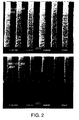
- Figures 2 and 3 illustrate that the compositions of Examples 1 and 2, respectively, are cleaning compositions that are effective at removing etch and ash residue from the surface of a semiconductor wafer.
- Table 2 demonstrates that the compositions of Examples 1 and 2 effectively clean without etching the metals on the substrate.
- composition of Comparative Example A is similar to that of Example 1 except for the urea derivative component.
- the composition of Comparative Example A employs a cyclic urea such as, for example, the kind disclosed in U.S. Patent No. 6,423,480 , as the cleaning agent.
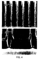
- Figure 4 illustrates that such cyclic ureas are ineffective at removing etch and ash residue from the surface of a semiconductor wafer.
- Comparative Examples B, C, and D compare the cleaning performance of compositions disclosed in the U.S. patent application Publication No. 2001/0014534 ("the 534 publication").
- Figure 5 shows the result of cleaning a semiconductor wafer with the composition of Comparative Example C, which employed urea at 35% of the composition.
- a Comparison of Figure 5 with Figures 2 and 3 demonstrates that the cleaning compositions of the present invention are more effective at removing etch and ash residue from the surface of a semiconductor wafer. This result is consistent with the teachings of the 534 publication, which relies on N-methyl-ethanolamine as the cleaning agent.
- compositions of Comparative Examples B and D were prepared to analyze the cleaning performance of urea.
- the composition of Comparative Example B consists of urea, gallic acid, and water and was prepared to evaluate composition 2 at Table 1 of the 534 publication without the cleaning agent, monoethanolamine, to see whether the urea would clean.
- the composition of Comparative Example D is similar to Example 2 except that the urea derivative component of Example 2 was replaced with urea. Neither of Comparative Examples B or D could be evaluated because all of the components were not soluble in the solution.
Landscapes
- Chemical & Material Sciences (AREA)
- Life Sciences & Earth Sciences (AREA)
- Engineering & Computer Science (AREA)
- Chemical Kinetics & Catalysis (AREA)
- Oil, Petroleum & Natural Gas (AREA)
- Wood Science & Technology (AREA)
- Organic Chemistry (AREA)
- Inorganic Chemistry (AREA)
- Detergent Compositions (AREA)
- Cleaning Or Drying Semiconductors (AREA)
- Organic Low-Molecular-Weight Compounds And Preparation Thereof (AREA)
- Epoxy Compounds (AREA)
- Drying Of Semiconductors (AREA)
- Weting (AREA)
- Exposure Of Semiconductors, Excluding Electron Or Ion Beam Exposure (AREA)
- Photosensitive Polymer And Photoresist Processing (AREA)
Abstract
Description
- The present invention provides cleaning compositions that can be used for a variety of applications including, for example, removing unwanted resist films, post-etch, and post-ash residue on a semiconductor substrate. In particular, the present invention provides cleaning compositions that comprise a urea derivative as a cleaning agent.
- The background of the present invention will be described in connection with its use in cleaning applications involving the manufacture of integrated circuits. It should be understood, however, that the use of the present invention has wider applicability as described hereinafter.
- In the manufacture of integrated circuits, it is sometimes necessary to etch openings or other geometries in a thin film deposited or grown on the surface of silicon, gallium arsenide, glass, or other substrate located on an in-process integrated circuit wafer. Present methods for etching such a film require that the film be exposed to a chemical etching agent to remove portions of the film. The particular etching agent used to remove the portions of the film depends upon the nature of the film. In the case of an oxide film, for example, the etching agent may be hydrofluoric acid. In the case of a polysilicon film, it will typically be hydrofluoric acid or a mixture of nitric acid and acetic acid.
- In order to assure that only desired portions of the film are removed, a photolithography process is used, through which a pattern in a computer drafted photo mask is transferred to the surface of the film. The mask serves to identify the areas of the film which are to be selectively removed. This pattern is formed with a photoresist material, which is a light sensitive material spun onto the in-process integrated circuit wafer in a thin film and exposed to high intensity radiation projected through the photo mask. The exposed or unexposed photoresist material, depending on its composition, is typically dissolved with developers, leaving a pattern which allows etching to take place in the selected areas, while preventing etching in other areas. Positive-type resists, for example, have been extensively used as masking materials to delineate patterns on a substrate that, when etching occurs, will become vias, trenches, contact holes, etc.
- Increasingly, a dry etching process such as, for example, plasma etching, reactive ion etching, or ion milling is used to attack the photoresist-unprotected area of the substrate to form the vias, trenches, contact holes, etc.. As a result of the plasma etching process, photoresist, etching gas and etched material by-products are deposited as residues around or on the sidewall of the etched openings on the substrate.
- Such dry etching processes also typically render the resist mask extremely difficult to remove. For example, in complex semiconductor devices such as advanced DRAMS and logic devices with multiple layers of back end lines of interconnect wiring, reactive ion etching (RIE) is used to produce vias through the interlayer dielectric to provide contact between one level of silicon, silicide or metal wiring to the next level of wiring. These vias typically expose, Al, AlCu, Cu, Ti, TiN, Ta, TaN, silicon or a silicide such as, for example, a silicide of tungsten, titanium or cobalt. The RIE process leaves a residue on the involved substrate comprising a complex mixture that may include, for example, re-sputtered oxide material, polymeric material derived from the etch gas, and organic material from the resist used to delineate the vias.
- Additionally, following the termination of the etching step, the photoresist and etch residues must be removed from the protected area of the wafer so that the final finishing operation can take place. This can be accomplished in a plasma "ashing" step by the use of suitable plasma ashing gases. This typically occurs at high temperatures, for example, above 200°C. Ashing converts most of the organic residues to volatile species, but leaves behind on the substrate a predominantly inorganic residue. Such residue typically remains not only on the surface of the substrate, but also on inside walls of vias that may be present. As a result, ash-treated substrates are often treated with a cleaning composition typically referred to as a "liquid stripping composition" to remove the highly adherent residue from the substrate. Finding a suitable cleaning composition for removal of this residue without adversely affecting, e.g., corroding, dissolving or dulling, the metal circuitry has also proven problematic. Failure to completely remove or neutralize the residue can result in discontinuances in the circuitry wiring and undesirable increases in electrical resistance.
- Prior art stripping compositions have included, for example: (a) organic sulfonic acid-based stripping solutions that contain an alkyl benzenesulfonic acid as the main stripping component; and (b) organic amine-based stripping solutions that contain an amine such as monoethanol amine as the main stripping component. Such prior art stripping compositions for removing the etching residue suffer, however, from significant drawbacks. For example, their use tends to erode copper wire exposed on the bottoms of via holes.
- Cleaning compositions containing dimethyl acetamide (DMAC) are used widely for removing residue from semiconductor substrates. DMAC is particularly suitable for such applications because it is highly polar, which makes it an excellent solvent for organic residues. DMAC is also desirable because it has a high flashpoint, it is water soluble, it has a low viscosity, and it is relatively inexpensive. Unfortunately, however, DMAC is classified as a toxic material in both the United States and in Europe. In this regard, DMAC has an NPFA health rating of 2 and its MSDS indicates that it is easily absorbed through the skin. Toxicity data also suggests that DMAC may be an embryotoxin and, as such, its use has been discouraged in Europe and has received extensive scrutiny in the United States and Asia. As a result, the electronic industry, for example, will not use cleaning compositions that include DMAC.
- Therefore, there is a need in the art for a cleaning composition that is non-toxic and environmentally friendly for back-end cleaning operations including stripping photoresist and plasma ash residue such as, for example, those generated by plasma processes.
- The present invention satisfies this need by providing a composition useful for removing residue from a semiconductor substrate comprising, in effective cleaning amounts, water, at least one urea derivative as the cleaning component, and a fluoride source. The composition according to the present invention includes optionally other materials such as, for example, one or more of a water-miscible organic solvent, a buffering agent, and a corrosion-inhibitor.
- In one embodiment, the present invention provides a composition which is useful for removing residue from a semiconductor substrate and which comprises, in effective cleaning amounts, water; at least one compound of formula (I) which functions as a cleaning agent:

- In another embodiment, the present invention provides a method for removing unwanted residues from a substrate such as, for example, a semiconductor substrate. The method includes the steps of contacting the substrate with a composition according to the present invention, rinsing the cleaning composition from the substrate, and drying the substrate.
- The composition of the present invention has excellent cleaning properties, is less toxic, and is more environmentally acceptable than compositions that are currently being used in the semiconductor industry.
- Results of the use of cleaning compositions within the scope of the present invention and of comparative compositions are illustrated in the accompanying drawings, which consist of the following Figures:
- Figure 1 includes SEM photographs at different magnifications of a semiconductor substrate with unwanted residue prior to a cleaning operation;
- Figure 2 includes SEM photographs at different magnifications of a semiconductor substrate after cleaning with a cleaning composition according to the present invention;
- Figure 3 includes SEM photographs at different magnifications of a semiconductor substrate after cleaning with a cleaning composition according to the present invention;
- Figure 4 includes SEM photographs at different magnifications of a semiconductor substrate after cleaning with the composition of Comparative Example A; and
- Figure 5 includes SEM photographs at different magnifications of a semiconductor substrate after cleaning with the composition of Comparative Example C.
- The present invention provides a composition whose components are present in amounts that effectively remove residue from a substrate such as, for example, a semiconductor substrate. In applications concerning semiconductor substrates, such residues include, for example, photoresist residues, ash residues, and etch residues such as, for example, residues caused by reactive ion etching. Moreover, a semiconductor substrate also includes metal, silicon, silicate and/or inter-level dielectric material such as deposited silicon oxides, which will also come into contact with the cleaning composition. Typical metals include copper, copper alloy, titanium, titanium nitride, tantalum, tantalum nitride, aluminum and/or aluminum alloy. The cleaning composition of the present invention is compatible with such materials as they exhibit a low metal and/or dielectric etch rate.
- The cleaning composition of the present invention is aqueous-based and, thus, comprises water. In the present invention, water functions in various ways such as, for example, to dissolve one or more solid components of the composition, as a carrier of the components, as an aid in the removal of the residue, as a viscosity modifier of the composition, and as a diluent. Preferably, the water employed in the cleaning composition is de-ionized (DI) water.
- It is believed that, for most applications, water will comprise, for example, from 10 to 90% by wt. of the composition. Some preferred embodiments of the present invention could comprise from 18 to 90% by wt. of water,more preferably from 35 to 60% by wt. of water. Other preferred embodiments of the present invention could comprise from 12 to 25% by wt. of water. Still other preferred embodiments of the present invention could include water in an amount to achieve the desired weight percent of the other ingredients.
- The cleaning composition of the present invention comprises an urea derivative that functions as a cleaning agent that principally solubilizes or aids in solubilizing organic residue that is present on the substrate. Preferably, the urea derivative is a compound of formula (I):

- Preferred urea derivatives according to formula (1) include 1,1-dimethylurea, 1,3-dimethylurea, 1,1,3-trimethylurea, 1,1,3,3-tetramethylurea, 1,3-bis(2-hydroxyethyl) urea, and 1-methyl-3-(2-hydroxypropyl) urea, and mixtures thereof. The most preferred urea derivative is 1,3-dimethylurea.
- It is believed that, for most applications, the amount of the urea derivative will comprise from 2 to 75% by weight of the composition. Preferably the urea derivative comprises from 5 to 70% by weight and, most preferably, from 5% to 67% by weight of the composition.
- The urea derivative for use in the composition of the present invention is relatively non-toxic compared to conventional organic solvent-based cleaning agents such as, for example, DMAC or N-methyl pyrrolidone and they have excellent cleaning properties. In preferred form, they are highly polar, have high solubility in water, and are biodegradable.
- The cleaning composition of the present invention also comprises one or more sources of fluoride ion. Fluoride ion functions principally to assist in removing inorganic residues from the substrate. Typical compounds that provide a fluoride ion source according to the present invention are hydrofluoric acid and salts thereof, ammonium fluoride, quaternary ammonium fluorides such as, for example, tetramethylammonium fluoride and tetrabutylammonium fluoride, fluoroborates, fluoroboric acid, tetrabutylammonium tetrafluoroborate, and aluminum hexafluoride. Also, a fluoride salt of an aliphatic primary, secondary or tertiary amine can be used, for example, an amine of the formula:
R5N(R6)R7
wherein R5, R6 and R7 individually represent H or a (C1-C4) alkyl group. Typically, the total number of carbon atoms in the R5, R6 and R7 groups is 12 carbon atoms or less. - In a preferred embodiment, the fluoride ion source is ammonium fluoride; however, when ammonium fluoride is used, it is preferable to remove ammonium ions from the system. Although this can be accomplished by allowing the prepared cleaning composition to stand at room temperature for a long period of time, they can also be removed by heating the solution.
- In selecting the source of the fluoride ion, consideration should be given as to whether or not the source would tend to release ions which would tend to affect adversely the surface being cleaned. For example, in cleaning semiconductor elements, the presence of sodium or calcium ions in the cleaning composition can have an adverse effect on the surface of the element.
- It is believed that the amount of the compound used as the source of the fluoride ion in the cleaning composition will, for the most applications, comprise, 0.1 to 5% by weight. Preferably, the compound comprises from 0.1 to 3% by weight and, most preferably, from 0.1 to 2.5% by weight. It should be understood that the amount of fluoride ion used will typically depend, however, on the particular substrate being cleaned. For example, in certain cleaning applications, the amount of the fluoride ion can be relatively high when cleaning substrates that comprise dielectric materials that have a high resistance to fluoride etching. Conversely, in other applications, the amount of fluoride ion should be relatively low, for example, when cleaning substrates that comprise dielectric materials that have a low resistance to fluoride etching.
- The cleaning composition of the present invention optionally includes one or more water-miscible organic solvents. In various embodiments of the present invention, metal lines on the substrate typically dictate whether a water-miscible organic solvent is used. For example, when aluminum lines are present on a substrate, the combination of water and fluoride ion will typically tend to etch the aluminum. In such embodiments, the use of water-miscible organic solvent can significantly reduce, if not eliminate, etching of aluminum.
- Examples of water-miscible organic solvents that can be used are ethylene glycol, propylene glycol, 1,4-butanediol, tripropylene glycol methyl ether, propylene glycol propyl ether, diethylene gycol n-butyl ether (e.g. commercially available under the trade designation Dowanol DB), hexyloxypropylamine, poly(oxyethylene)diamine, dimethylsulfoxide, tetrahydrofurfuryl alcohol, glycerol, alcohols, sulfoxides, or mixtures thereof. Preferred solvents are alcohols, diols, or mixtures thereof. Most preferred solvents are diols such as, for example, propylene glycol.
- It is believed that, for most applications, the amount of water-miscible organic solvent will comprise from 5 to 75% by weight of the composition. Preferably, the solvent comprises from 5 to 70% or from 10 to 75% by weight and, most preferably, from 5% to 67% by weight of the composition.
- In addition, the cleaning composition of the present invention optionally includes a buffering agent to control the pH of the composition, typically to within a range of from 3 to 6 and, more typically, from 3.5 to 5.5. There are various applications in which the use of buffering is advantageous, indeed even quite important. For example, in some applications, pH drift can cause significant and undesirable variances in cleaning and substrate etching; a semi-aqueous fluoride-containing stripper at pH of 4.75 may not etch copper significantly, but at pH of 7.5 or higher, the stripper may severely attack copper, causing unacceptable loss of a device critical dimension.
- Buffering agents for use in the present invention typically comprise a weak acid and a soluble salt containing the conjugate base of the weak acid. For example, the buffering agent can comprise a weak organic monoacid and its conjugate base such as, for example, acetic acid and ammonium acetate. In other embodiments, the buffering agent may comprise an organic or inorganic base in combination with an organic diacid. Examples of suitable bases include: ammonium hydroxide, amines, and quaternary ammonium hydroxides. In semiconductor applications, it is preferred that the base not include metal ions, for example, sodium and potassium, because they tend to contaminate the substrate. Preferred bases are ammonium hydroxide and monoethanolamine (MEA).
- The pH of the cleaning composition can vary anywhere from 1 to 7, or, more typically, 5.5 to 6.0, depending on the specific mono or diacid chosen and its effective buffering range. Diacids, for example, are defined by two pKa values and a buffer is generally formed about 0.75 pH units on either side of a given pKa. For example, the pK values for malonic acid are pK1=2.8 and pK2=5.7. One can then expect malonic acid to act as a buffer between the pHs of 2.05-3.55 and again between 4.95-6.45. Similarly, the pK values for adipic acid are pK1=4.5 and pK2=5.5. Since the two pHs almost overlap, the effective buffering range of adipic acid is between the pHs of 3.75 and 6.25.
- It is believed that for most applications, the buffering agent, will comprise from 0.2 to 30% by weight of the composition; preferably, it comprises from 0.5 to 30% by weight; most preferably, from 0.5 to 28% by weight of the composition.
- The cleaning composition of the present invention also optionally includes a corrosion-inhibitor. The use of a corrosion-inhibitor is preferred when the composition is used to clean a metallic substrate. Examples of corrosion-inhibitors include aromatic hydroxyl compounds, acetylenic alcohols, carboxyl group-containing organic compounds and anhydrides thereof, and triazole compounds.
- Exemplary aromatic hydroxyl compounds include phenol, cresol, xylenol, pyrocatechol, resorcinol, hydroquinone, pyrogallol, 1.2.4-benzenetriol, salicyl alcohol, p-hydroxybenzyl alcohol, o-hydroxybenzyl alcohol, p-hydroxyphenethyl alcohol, p-aminophenol, m-aminophenol, diaminophenol, amino resorcinol, p-hydroxybenzoic acid, o-hydroxybenzoic acid 2,4-dihydroxybenzoic acid, 2,5-dihydroxybenzoic acid, 3,4-dihydroxybenzoic acid and 3,5-dihydroxybenzoic acid.
- Exemplary acetylenic alcohols include 2-butyne-1,4-diol, 3,5-dimethyl-1-hexyn-3-ol, 2-methyl-3-butyn-2-ol, 3-methyl-1-pentyn-3-ol, 3,6-dimethyl-4-octyn-3,6-diol, 2,4-,7,9-tetramethyl-5-decyne-4,7-diol and 2,5-dimethyl-3-hexyne-2,5-diol.
- Exemplary carboxyl group-containing organic compounds and anhydrides thereof include formic acid, acetic acid, propionic acid, butyric acid, isobutyric acid, oxalic acid, malonic acid, succinic acid, glutaric acid, maleic acid, fumaric acid, benzoic acid, phthalic acid, 1,2,3-benzenetricarboxylic acid, glycolic acid, lactic acid, maleic acid citric acid, acetic anhydride and salicylic acid.
- Exemplary triazole compounds include benzotriazole, o-tolyltriazole, m-tolyltriazole, p-tolyltriazole, carboxybenzotriazole, 1-hydroxybenzotriazole, nitrobenzotriazole and dihydroxypropylbenzotriazole.
- Preferred inhibitors are catechol, gallic acid, benzotriazole, pyrogallol, 4-methyl catechol fumaric acid and diethylhydroxylamine (DEHA); it is preferred that an inhibitor other than benzotriazole be used when cleaning a substrate comprising copper because benzotriazole has a tendency to bind to copper.
- It is believed that for most applications, the corrosion-inhibitor will comprise from 0.01 to 5% by weight of the composition; preferably it comprises from 0.01 to 4% by weight, more preferably, from 0.01 3% by weight of the composition, and most preferably from 0.01 to 2.5% by weight.
- Another optional ingredient that can be used in the cleaning composition is a metal chelating agent; it can function to increase the capacity of the composition to retain metals in solution and to enhance the dissolution of metallic residues. Typical examples of chelating agents useful for this purpose are the following organic acids and their isomers and salts: (ethylenedinitrilo)tetraacetic acid (EDTA), butylenediaminetetraacetic acid, (1,2-cyclohexylenedinitrilo-)tetraacetic acid (CyDTA), diethylenetriaminepentaacetic acid (DETPA), ethylenediaminetetrapropionic acid, (hydroxyethyl)ethylenediaminetriacetic acid (HEDTA), N,N,N',N'-ethylenediaminetetra(methylenephosphonic) acid (EDTMP), triethylenetetraminehexaacetic acid (TTHA), 1,3-diamino-2-hydroxypropane-N,N,N',N'-tetraacetic acid (DHPTA), methyliminodiacetic acid, propylenediaminetetraacetic acid, nitrolotriacetic acid (NTA), citric acid, tartaric acid, gluconic acid, saccharic acid, glyceric acid, oxalic acid, phthalic acid, maleic acid, mandelic acid, malonic acid, lactic acid, salicylic acid, catechol, gallic acid, propyl gallate, pyrogallol, 8-hydroxyquinoline, and cysteine. Preferred chelating agents are aminocarboxylic acids such as EDTA, CyDTA and aminophosphonic acids such as EDTMP.
- It is believed that, for most applications, the chelating agent will be present in the composition in an amount of from 0 to 5% by weight, preferably in an amount of from 0.1 to 2% by weight of the composition.
- Other commonly known components such as dyes, biocides etc. can be included in the cleaning composition in conventional amounts, for example, amounts up to a total of about 5 weight % of the composition.
- The cleaning composition of the present invention is typically prepared by mixing the components together in a vessel at room temperature until all solids have dissolved in the aqueous-based medium.
- The cleaning composition of the present invention can be used to remove from a substrate undesired residue. It is believed that the composition can be used to particularly good advantage in cleaning a semiconductor substrate on which residue is deposited or formed during the process for manufacturing semiconductor devices; examples of such residue include resist compositions in the form of films (both positive and negative) and etching deposits formed during dry etching, as well as chemically degraded resist films. The use of the composition is particularly effective when the residue to be removed is a resist film and/or an etching deposit on a semiconductor substrate having a metal film-exposed surface. Examples of substrates that can be cleaned by use of the composition of the present invention without attacking the substrates themselves include metal substrates, for example: aluminum titanium/tungsten; aluminum/silicon; aluminum/silicon/copper; silicon oxide; silicon nitride; and gallium/arsenide. Such substrates typically include residues comprising photoresists and/or post etch deposits.
- Examples of resist compositions that can be effectively removed by use of the cleaning composition of the present invention include photoresists containing esters or ortho-naphthoquinones and novolak-type binders and chemically amplified resists containing blocked polyhydroxystyrene or copolymers of polyhydroxystyrene and photoacid generators. Examples of commercially available photoresist compositions include Clariant Corporation AZ 1518, AZ 4620, Shipley Company, Inc. photoresists, S1400, APEX-E™ positive DUV, UV5™ positive DUV, Megaposit™ SPR™ 220 Series; JSR Microelectronics photoresists KRF™ Series, ARF™ Series; and Tokyo Ohka Kogyo Co., Ltd. Photoresists TSCR Series and TDUR-P/N Series.
- In addition to being effective when used to remove resist films and/or etching residues on a semiconductor wafer having an exposed surface of a metal film, the cleaning composition is especially effective when the metal film is made of copper or a copper alloy containing copper as the main component and also when a low-dielectric film is used as an interlayer insulating film. An example of a copper alloy containing copper as the main component is one containing 90% by weight or more copper, and other elements, for example, Sn, Ag, Mg, Ni, Co, Ti, Si, and Al. Since these metals have low resistances and improve the high-speed operation of elements, but are easily dissolved or corroded by chemicals, the "non-corrosive" properties of the composition of the present invention are significant.
- The cleaning composition can be used to remove post-etch and ash, other organic and inorganic residues as well as polymeric residues from semiconductor substrates at relatively low temperatures with little corrosive effect. The cleaning composition should be applied to the surface for a period of time to sufficient to obtain the desired cleaning effect. The time will vary depending on numerous factors, including, for example, the nature of the residue the temperature of the cleaning composition and the particular cleaning composition used. In general, the cleaning composition can be used, for example, by contacting the substrate at a temperature of from 25° C to 85° C for a period of time ranging from 1 minute to 1 hour followed by rinsing the cleaning composition from the substrate and drying the substrate.
- The contacting step can be carried out by any suitable means such as, for example, immersion, spray, or via a single wafer process; any method that utilizes a liquid for removal of photoresist, ash or etch deposits and/or contaminants can be used.
- The rinsing step is carried out by any suitable means, for example, rinsing the substrate with de-ionized water by immersion or spray techniques. In preferred embodiments, the rinsing step is carried out employing a mixture of de-ionized water and a water-miscible organic solvent such as, for example, isopropyl alcohol.
- The drying step is carried out by any suitable means, for example, isopropyl alcohol (IPA) vapor drying or by centripetal force.
- It will be appreciated by those skilled in the art that the cleaning composition of the present invention may be modified to achieve optimum cleaning without damaging the substrate so that high throughput cleaning can be maintained in the manufacturing process. For example, one skilled in the art would appreciate that, for example, modifications to the amounts of some or all of the components may be made depending upon the composition of the substrate being cleaned, the nature of the residue to be removed, and the particular process parameters used.
- Although the present invention has been principally described in connection with cleaning semiconductor substrates, the cleaning compositions of the invention can be employed to clean any substrate that includes organic and inorganic residues.
- The following examples are provided for the purpose of further illustrating the present invention but are by no means intended to limit the same.
- All compositions which are the subject of the present Examples were prepared by mixing 500g of material in a 600mL beaker with a 1" (2½cm) Teflon™-coated stir bar. For compositions without a water-miscible organic solvent, the first material added to the beaker was deionized (DI) water. Dimethyl urea, which is highly soluble in water, was added next. When using relatively large amounts of solid dimethyl urea (DMU), it is recommended that the DMU be added to the water as it is stirred until the aqueous solution is clear. The remaining components can then be added in any order, but the preferred order, as used in the present examples, is (1) acetic acid, (2) ammonium fluoride, (40%), and (3) ammonium acetate, if used.
- For compositions that include a water-miscible organic solvent, the composition is mixed as stated above, but the solvent such as, for example, propylene glycol, is preferably added to the water before the dimethyl urea is introduced. The resulting solution will take a bit longer to turn clear since the urea is not as soluble in propylene glycol as it is in water.
- Each substrate used in the present Examples comprised an organosilicate glass (OSG) dielectric material with a titanium nitride capping layer that was deposited on a silicon nitride substrate. The OSG was etched by reactive ion etching (RIE) to leave behind OSG lines capped with titanium nitride. Following RIE, the substrates were treated in a plasma to ash the photoresist. Figure 1 shows the residues on the substrate prior to cleaning.
- Cleaning tests were run using 305 mL of the cleaning compositions in a 400mL beaker with a ½" (11/4cm) round Teflon™ stir bar set at 600 rpm. The cleaning compositions were heated to the desired temperature indicated below on a hot plate if necessary. Wafer segments approximately ½" x ½" (11/4cm x 11/4cm ) in size were immersed in the compositions under the following set of conditions.
- 10 minutes @ 25°C
- 20 minutes @ 25°C
- 10 minutes @ 35°C
- 20 minutes @ 35°C
- The segments were then rinsed for 3 minutes in a Dl water overflow bath and subsequently dried using filtered nitrogen. They were then analyzed for cleanliness using SEM microscopy.
- Coupons of the blanket Al or blanket Cu wafers were measured for metal layer thickness by measuring the resistivity of the layer by employing a ResMap™ model 273 resistivity instrument from Creative Design Engineering, Inc. The coupons were then immersed in the composition at the desired temperature for up to one hour. Periodically the coupons were removed from the composition, rinsed with de-ionized water and dried and the thickness of the metal layer was again measured. A graph of the change in thickness as a function of immersion time was made and the etch rate in Angstroms/min (0.1 nm/min) was determined from the slope of the curve.
- Table 1 identifies the components of the composition tested and referenced below.
Table 1 Component Example 1 Example 2 Comp. Example A Comp. Example B Comp. Example C Comp. Example D Dimethyl Ureaa 36.95 36.95 Cyclic Ureab 73.9 Urea 35 35 36.95 Water 61.95 25.0 25.0 60 65 25.0 Propylene Glycol 36.95 36.95 Acetic Acid 0.5 0.5 0.5 0.5 Ammonium Fluoride Aq. Sol. (40%) 0.4 0.4 0.4 0.4 Ammonium Acetate 0.2 0.2 0.2 0.2 Gallic Acid 5 Cleanability Excellent Excellent Poor Not Soluble Poor Not Soluble a = 1,3-dimethyl urea
b = 1-2-Hydroxyethyl)-2-imidazolidinone (75% aqueous solution) - Tables 2 and 3 summarize etch rates of Examples 1 and 2, respectively.
Table 2 Formulation of Example 1 Substrate Temp. (°C) Etch Rate (Å/min) Al 25 409 Cu 25 1 Coral 25 < 1 Coral 35 < 1 TEOS* 25 1 TEOS* 40 2 TEOS** 25 2 TEOS** 40 7 * = Undoped, Undensified
** = P-doped, UndensifiedTable 3 Formulation of Example 2 Substrate Temp. (ºC) Etch Rate (Å/min) Al 25 12 Al 35 21 Cu 25 2 Cu 35 3 - The compositions of Examples 1 and 2 are cleaning compositions according to the present invention wherein dimethyl urea is the cleaning agent. Figures 2 and 3 illustrate that the compositions of Examples 1 and 2, respectively, are cleaning compositions that are effective at removing etch and ash residue from the surface of a semiconductor wafer. Table 2 demonstrates that the compositions of Examples 1 and 2 effectively clean without etching the metals on the substrate.
- The composition of Comparative Example A is similar to that of Example 1 except for the urea derivative component. In this regard, the composition of Comparative Example A employs a cyclic urea such as, for example, the kind disclosed in
U.S. Patent No. 6,423,480 , as the cleaning agent. Figure 4 illustrates that such cyclic ureas are ineffective at removing etch and ash residue from the surface of a semiconductor wafer. - Comparative Examples B, C, and D compare the cleaning performance of compositions disclosed in the
U.S. patent application Publication No. 2001/0014534 ("the 534 publication"). Figure 5 shows the result of cleaning a semiconductor wafer with the composition of Comparative Example C, which employed urea at 35% of the composition. A Comparison of Figure 5 with Figures 2 and 3 demonstrates that the cleaning compositions of the present invention are more effective at removing etch and ash residue from the surface of a semiconductor wafer. This result is consistent with the teachings of the 534 publication, which relies on N-methyl-ethanolamine as the cleaning agent. - The compositions of Comparative Examples B and D were prepared to analyze the cleaning performance of urea. The composition of Comparative Example B consists of urea, gallic acid, and water and was prepared to evaluate composition 2 at Table 1 of the 534 publication without the cleaning agent, monoethanolamine, to see whether the urea would clean. The composition of Comparative Example D is similar to Example 2 except that the urea derivative component of Example 2 was replaced with urea. Neither of Comparative Examples B or D could be evaluated because all of the components were not soluble in the solution.
- The foregoing examples and description of the preferred embodiments should be taken as illustrating, rather than as limiting the present invention as defined by the claims. As will be readily appreciated, numerous variations and combinations of the features set forth above can be utilized without departing from the present invention as set forth in the claims. Such variations are not regarded as a departure from the scope of the invention, and all such variations are intended to be included within the scope of the following claims.
Claims (21)
- A composition useful for removing residue from a semiconductor substrate comprising in effective cleaning amounts:a) water;b) at least one compound of formula (I):
 R1 and R3 are independently hydrogen, C1-C4 alkyl, or C1-C4 alkylol; andR2 and R4 are independently C1-C4 alkyl, or C1-C4 alkylol;c) a fluoride ion source;d) optionally a water-miscible organic solvent;e) optionally a buffering agent; andf) optionally a corrosion inhibitor.
 - The composition of claim 1, wherein the compound of formula (I) is selected from 1,1-dimethylurea, 1,3-dimethylurea, 1,1,3-trimethylurea, 1,1,3,3-tetramethylurea, 1,3-bis(2-hydroxyethyl) urea, 1-methyl, 3-(2-hydroxypropyl) urea, and mixtures thereof.
- The composition of claim 2, wherein the compound of formula (I) is selected from 1,1-dimethylurea and 1,3-dimethylurea.
- The composition of any preceding claim, wherein the fluoride ion source is selected from hydrofluoric acid, tetramethylammonium fluoride, tetrabutylammonium fluoride, fluoroborates, fluoroboric acid, aluminum hexafluoride, ammonium fluoride, methylamine hydrofluoride, ethylamine hydrofluoride, propylamine hydrofluoride and a fluoride salt of an aliphatic primary, secondary or tertiary amine having the formula R5N(R6)R7, wherein R5, R6 and R7 each represent individually H or a (C1-C4) alkyl group.
- The composition of claim 4, wherein the fluoride ion source is ammonium fluoride.
- The composition of any preceding claim, including a water-miscible organic solvent which is selected from propylene glycol, tripropylene glycol methyl ether, 1,4-butanediol, propylene glycol propyl ether, diethylene gycol n-butyl ether, hexyloxypropylamine, poly(oxyethylene)diamine, tetrahydrofurfuryl alcohol, and mixtures thereof.
- The composition of claim 6, wherein the water-miscible organic solvent which is propylene glycol.
- The composition of any preceding claim, including a buffering agent comprising a diacid.
- The composition of any one of claims 1 to 7, including a buffering agent which comprises acetic acid and ammonium acetate.
- The composition of any preceding claim, including a corrosion inhibitor selected from aromatic hydroxyl compounds, acetylenic alcohols, carboxyl group containing organic compounds and anhydrides thereof, triazole compounds, and mixtures thereof.
- The composition of claim 10 wherein the corrosion inhibitor is selected from catechol, gallic acid, pyrogallol, 4-methyl catechol fumaric acid, diethylhydroxylamine, and mixtures thereof.
- A cleaning composition according to claim 1, the composition comprising:a) from 10.0% by wt. to 90.0% by wt. of water;b) from 2.0% by wt. to 75.0% by wt. of a compound of formula (1);c) from 0.1 % by wt. to 5.0% by wt. of a fluoride ion source;d) optionally from 5.0% by wt. to 75.0% by wt. of at least one water-miscible organic solvent;e) optionally from 0.2% by wt. to 30.0% by wt. of a buffering agent; andf) optionally from 0.01 % by wt. to 5.0% by wt. of a corrosion inhibitor.
- The composition of claim 12, consisting essentially of:a) from 18.0% by wt. to 90.0% by wt. of water;b) from 5.0% by wt. to 67.0% by wt. of the compound of formula (I);c) from 0.1 % by wt. to 2.5% by wt. of a fluoride ion source;d) from 0.5% by wt. to 28.0% by wt. of a buffering agent; ande) from 0.01 % by wt. to 2.5% by wt. of a corrosion inhibitor.
- The composition of claim 12, consisting essentially of:a) from 12.0% by wt. to 25.0% by wt. of water;b) from 5.0% by wt. to 67.0% by wt. of the compound of formula (I);c) from 0.1 % by wt. to 2.5% by wt. of a fluoride ion source;d) from 5.0% by wt. to 67.0% by wt. of at least one water-miscible organic solvent;e) from 0.5% by wt. to 28.0% by wt. of a buffering agent; andf) from 0.01 % by wt. to 2.5% by wt. of a corrosion inhibitor.
- The composition of any one of claims 12 to 14, wherein the compound of formula (I), the fluoride ion source, the water-miscible organic solvent, the buffering agent, and/or the corrosion inhibitor are as defined in any one of claims 2 to 11.
- The composition of any preceding claim claim, further including a chelating agent.
- A method for removing residue from a substrate, the method comprising the steps of:contacting the substrate with a cleaning composition comprising:a) from 10.0% by wt. to 90.0% by wt. of water;b) from 2.0% by wt. to 75% by wt. of a compound of formula (1):
 R1 and R3 are independently hydrogen, C1-C4 alkyl, or C1-C4 alkylol; andR2 and R4 are independently C1-C4 alkyl, or C1-C4 alkylol;c) from 0.1 % by wt. to 5.0% by wt. of a fluoride ion source;d) optionally from 5.0% by wt. to 75.0% by wt. of at least one water-miscible organic solvent;e) optionally from 0.2% by wt. to 30.0% by wt. of a buffering agent; andf) optionally from 0.01 % by wt. to 5.0% by wt. of a corrosion inhibitor; rinsing the cleaning composition from the substrate; anddrying the substrate.
 - The method of claim 17, wherein the substrate is a semiconductor substrate.
- The method of claim 17 or 18, wherein the cleaning composition is as further defined in claim 13 or 14.
- The method of claim 17, 18 or 19, wherein the compound of formula (I), the fluoride ion source, the water-miscible organic solvent, the buffering agent, and/or the corrosion inhibitor are as defined in any one of claims 2 to 11.
- The method of any one of claims 17 to 20, wherein the cleaning composition further includes a chelating agent.
Applications Claiming Priority (1)
| Application Number | Priority Date | Filing Date | Title |
|---|---|---|---|
| US11/342,414 US20070179072A1 (en) | 2006-01-30 | 2006-01-30 | Cleaning formulations |
Publications (2)
| Publication Number | Publication Date |
|---|---|
| EP1813667A1 true EP1813667A1 (en) | 2007-08-01 |
| EP1813667B1 EP1813667B1 (en) | 2009-09-30 |
Family
ID=38001890
Family Applications (1)
| Application Number | Title | Priority Date | Filing Date |
|---|---|---|---|
| EP07250386A Active EP1813667B1 (en) | 2006-01-30 | 2007-01-30 | Cleaning formulations |
Country Status (10)
| Country | Link |
|---|---|
| US (1) | US20070179072A1 (en) |
| EP (1) | EP1813667B1 (en) |
| JP (1) | JP2007243162A (en) |
| KR (1) | KR100857865B1 (en) |
| CN (1) | CN101013273A (en) |
| AT (1) | ATE444351T1 (en) |
| DE (1) | DE602007002572D1 (en) |
| IL (1) | IL180944A0 (en) |
| SG (1) | SG134279A1 (en) |
| TW (1) | TW200728456A (en) |
Cited By (4)
| Publication number | Priority date | Publication date | Assignee | Title |
|---|---|---|---|---|
| EP2217679A4 (en) * | 2007-11-07 | 2012-01-25 | Vitech Internat Inc | TETRAFLUOROBORATE COMPOUNDS, COMPOSITIONS AND METHODS OF RELATED USE |
| US8889609B2 (en) | 2011-03-16 | 2014-11-18 | Air Products And Chemicals, Inc. | Cleaning formulations and method of using the cleaning formulations |
| US9536730B2 (en) | 2012-10-23 | 2017-01-03 | Air Products And Chemicals, Inc. | Cleaning formulations |
| US20210395645A1 (en) * | 2019-03-26 | 2021-12-23 | Fujifilm Electronic Materials Co., Ltd. | Cleaning liquid |
Families Citing this family (26)
| Publication number | Priority date | Publication date | Assignee | Title |
|---|---|---|---|---|
| JP4988165B2 (en) * | 2005-03-11 | 2012-08-01 | 関東化学株式会社 | Photoresist stripping composition and method for stripping photoresist |
| CN101233456B (en) * | 2005-06-07 | 2013-01-02 | 高级技术材料公司 | Metal and dielectric compatible sacrificial antireflective coating cleaning and removal compositions |
| US8211844B2 (en) * | 2005-10-21 | 2012-07-03 | Freescale Semiconductor, Inc. | Method for cleaning a semiconductor structure and chemistry thereof |
| JP4828451B2 (en) * | 2006-03-27 | 2011-11-30 | 東京エレクトロン株式会社 | Substrate processing method, semiconductor device manufacturing method, and substrate processing apparatus |
| US7772128B2 (en) * | 2006-06-09 | 2010-08-10 | Lam Research Corporation | Semiconductor system with surface modification |
| US9058975B2 (en) * | 2006-06-09 | 2015-06-16 | Lam Research Corporation | Cleaning solution formulations for substrates |
| KR20100044777A (en) * | 2007-07-26 | 2010-04-30 | 미츠비시 가스 가가쿠 가부시키가이샤 | Composition for cleaning and rust prevention and process for producing semiconductor element or display element |
| US20090229629A1 (en) * | 2008-03-14 | 2009-09-17 | Air Products And Chemicals, Inc. | Stripper For Copper/Low k BEOL Clean |
| KR101426090B1 (en) * | 2008-04-18 | 2014-08-06 | 에스케이하이닉스 주식회사 | Cleaning liquid composition for phase change memory device and method for manufacturing phase change memory device using the same |
| US20110189049A1 (en) * | 2008-05-09 | 2011-08-04 | Martin Beaulieu | Method for treating odors |
| JP5206177B2 (en) * | 2008-07-09 | 2013-06-12 | 三菱瓦斯化学株式会社 | Resist stripping composition and method for manufacturing semiconductor device using the same |
| US8361237B2 (en) * | 2008-12-17 | 2013-01-29 | Air Products And Chemicals, Inc. | Wet clean compositions for CoWP and porous dielectrics |
| US8518865B2 (en) * | 2009-08-31 | 2013-08-27 | Air Products And Chemicals, Inc. | Water-rich stripping and cleaning formulation and method for using same |
| KR101829399B1 (en) * | 2010-03-04 | 2018-03-30 | 삼성전자주식회사 | photosensitive-resin remover composition and method of fabricating semiconductor device using the same |
| JP5513196B2 (en) | 2010-03-25 | 2014-06-04 | 富士フイルム株式会社 | Cleaning composition and method for manufacturing semiconductor device |
| CN101838111B (en) * | 2010-05-20 | 2012-06-27 | 合肥茂丰电子科技有限公司 | Glass substrate etching solution and preparation method thereof |
| DE102015106026B3 (en) | 2015-04-20 | 2016-08-25 | Interroll Holding Ag | Method for exchanging a control unit in a conveyor device |
| US10934484B2 (en) * | 2018-03-09 | 2021-03-02 | Versum Materials Us, Llc | Etching solution for selectively removing silicon-germanium alloy from a silicon-germanium/ germanium stack during manufacture of a semiconductor device |
| KR101906122B1 (en) | 2018-07-09 | 2018-12-07 | 와이엠티 주식회사 | Au BUMPED SURFACE CLEANING COMPOSITION AND CLEANING METHOD |
| CN109055954A (en) * | 2018-09-05 | 2018-12-21 | 合肥久新不锈钢厨具有限公司 | A kind of composite environmental-friendly stainless steel cleaner and its application method |
| CN109112557A (en) * | 2018-09-05 | 2019-01-01 | 合肥久新不锈钢厨具有限公司 | A kind of preparation method of novel antibacterial stainless steel detergent |
| CN109234048A (en) * | 2018-09-05 | 2019-01-18 | 合肥久新不锈钢厨具有限公司 | A kind of stainless steel cleanser compositions and its application |
| KR102930191B1 (en) | 2019-03-14 | 2026-02-25 | 닛산 가가쿠 가부시키가이샤 | Detergent composition and cleaning method |
| TWI850424B (en) * | 2019-07-15 | 2024-08-01 | 美商慧盛材料美國有限責任公司 | Compositions for removing etch residues, methods of using and use thereof |
| KR20220083186A (en) * | 2020-12-11 | 2022-06-20 | 동우 화인켐 주식회사 | Process solution for polymer processing |
| KR102925424B1 (en) | 2021-03-16 | 2026-02-11 | 동우 화인켐 주식회사 | Process solution composition for polymer processing |
Citations (6)
| Publication number | Priority date | Publication date | Assignee | Title |
|---|---|---|---|---|
| DE1227178B (en) * | 1963-10-11 | 1966-10-20 | Knapsack Ag | Liquid detergents |
| WO1996030488A1 (en) * | 1995-03-24 | 1996-10-03 | Atotech Usa Inc. | Aluminum desmut composition and process |
| US20010014534A1 (en) | 2000-01-25 | 2001-08-16 | Nec Corporation | Stripper composition and stripping method |
| US6423480B2 (en) | 1999-12-27 | 2002-07-23 | Sumitomo Chemical Company, Limited | Remover composition |
| DE10331033A1 (en) * | 2002-07-12 | 2004-02-12 | Renesas Technology Corp. | Cleaning composition, used for removing resist or residues of resist or from dry etching in semiconductor device production, contains fluoride of non-metal base, water-soluble organic solvent, acid and water |
| US20050096237A1 (en) * | 2003-10-30 | 2005-05-05 | Nissan Chemical Industries, Ltd. | Maleic acid and ethylene urea containing formulation for removing residue from semiconductor substrate and method for cleaning wafer |
Family Cites Families (23)
| Publication number | Priority date | Publication date | Assignee | Title |
|---|---|---|---|---|
| US3114657A (en) * | 1960-08-29 | 1963-12-17 | John W Stilwell | Composition and method for cleaning and stripping metals |
| US5308743A (en) * | 1989-06-29 | 1994-05-03 | Fuji Photo Film Co., Ltd. | Positive image-forming process utilizing glass substrate with oxide film of indium-tin alloy, coated with o-quinonediazide photoresist, with etching of the oxide film in the imagewise exposed areas |
| AU3661997A (en) * | 1996-07-25 | 1998-02-20 | Ekc Technology, Inc. | Chemical mechanical polishing composition and process |
| US6896826B2 (en) * | 1997-01-09 | 2005-05-24 | Advanced Technology Materials, Inc. | Aqueous cleaning composition containing copper-specific corrosion inhibitor for cleaning inorganic residues on semiconductor substrate |
| US6247042B1 (en) * | 1997-09-24 | 2001-06-12 | Microsoft Corporation | Method and system for restoring the state of physical memory as the focus changes among application programs in a computer |
| US6432828B2 (en) * | 1998-03-18 | 2002-08-13 | Cabot Microelectronics Corporation | Chemical mechanical polishing slurry useful for copper substrates |
| TWI227726B (en) * | 1999-07-08 | 2005-02-11 | Eternal Chemical Co Ltd | Chemical-mechanical abrasive composition and method |
| KR100555493B1 (en) * | 1999-12-22 | 2006-03-03 | 삼성전자주식회사 | Semiconductor substrate cleaning method |
| JP3869608B2 (en) * | 2000-01-25 | 2007-01-17 | Necエレクトロニクス株式会社 | Anticorrosive |
| AU2001273598A1 (en) * | 2000-06-29 | 2002-01-14 | Huntsman Petrochemical Corporation | Carbonate-based photoresist stripping compositions |
| TW573217B (en) * | 2000-12-27 | 2004-01-21 | Sumitomo Chemical Co | Remover composition |
| US6642199B2 (en) * | 2001-04-19 | 2003-11-04 | Hubbard-Hall, Inc. | Composition for stripping nickel from substrates and process |
| JP4810764B2 (en) * | 2001-06-29 | 2011-11-09 | 三菱瓦斯化学株式会社 | Resist stripper composition |
| MY143399A (en) * | 2001-07-09 | 2011-05-13 | Avantor Performance Mat Inc | Microelectronic cleaning compositons containing ammonia-free fluoride salts for selective photoresist stripping and plasma ash residue cleaning |
| US6692546B2 (en) * | 2001-08-14 | 2004-02-17 | Advanced Technology Materials, Inc. | Chemical mechanical polishing compositions for metal and associated materials and method of using same |
| KR100942124B1 (en) * | 2002-01-24 | 2010-02-16 | 제이에스알 가부시끼가이샤 | Radiation-sensitive composition, insulating film and display element for insulating film formation |
| US6800142B1 (en) * | 2002-05-30 | 2004-10-05 | Novellus Systems, Inc. | Method for removing photoresist and post-etch residue using activated peroxide followed by supercritical fluid treatment |
| JP2004029276A (en) * | 2002-06-25 | 2004-01-29 | Mitsubishi Gas Chem Co Inc | Fluorine-containing resist stripper for copper wiring boards |
| US6677286B1 (en) * | 2002-07-10 | 2004-01-13 | Air Products And Chemicals, Inc. | Compositions for removing etching residue and use thereof |
| US20040077295A1 (en) * | 2002-08-05 | 2004-04-22 | Hellring Stuart D. | Process for reducing dishing and erosion during chemical mechanical planarization |
| US20040055621A1 (en) * | 2002-09-24 | 2004-03-25 | Air Products And Chemicals, Inc. | Processing of semiconductor components with dense processing fluids and ultrasonic energy |
| US7166419B2 (en) * | 2002-09-26 | 2007-01-23 | Air Products And Chemicals, Inc. | Compositions substrate for removing etching residue and use thereof |
| US6951710B2 (en) * | 2003-05-23 | 2005-10-04 | Air Products And Chemicals, Inc. | Compositions suitable for removing photoresist, photoresist byproducts and etching residue, and use thereof |
-
2006
- 2006-01-30 US US11/342,414 patent/US20070179072A1/en not_active Abandoned
-
2007
- 2007-01-22 SG SG200700503-6A patent/SG134279A1/en unknown
- 2007-01-25 IL IL180944A patent/IL180944A0/en unknown
- 2007-01-29 TW TW096103247A patent/TW200728456A/en unknown
- 2007-01-29 JP JP2007017471A patent/JP2007243162A/en not_active Withdrawn
- 2007-01-30 AT AT07250386T patent/ATE444351T1/en not_active IP Right Cessation
- 2007-01-30 CN CNA2007100079263A patent/CN101013273A/en active Pending
- 2007-01-30 KR KR1020070009421A patent/KR100857865B1/en not_active Expired - Fee Related
- 2007-01-30 DE DE602007002572T patent/DE602007002572D1/en not_active Expired - Fee Related
- 2007-01-30 EP EP07250386A patent/EP1813667B1/en active Active
Patent Citations (6)
| Publication number | Priority date | Publication date | Assignee | Title |
|---|---|---|---|---|
| DE1227178B (en) * | 1963-10-11 | 1966-10-20 | Knapsack Ag | Liquid detergents |
| WO1996030488A1 (en) * | 1995-03-24 | 1996-10-03 | Atotech Usa Inc. | Aluminum desmut composition and process |
| US6423480B2 (en) | 1999-12-27 | 2002-07-23 | Sumitomo Chemical Company, Limited | Remover composition |
| US20010014534A1 (en) | 2000-01-25 | 2001-08-16 | Nec Corporation | Stripper composition and stripping method |
| DE10331033A1 (en) * | 2002-07-12 | 2004-02-12 | Renesas Technology Corp. | Cleaning composition, used for removing resist or residues of resist or from dry etching in semiconductor device production, contains fluoride of non-metal base, water-soluble organic solvent, acid and water |
| US20050096237A1 (en) * | 2003-10-30 | 2005-05-05 | Nissan Chemical Industries, Ltd. | Maleic acid and ethylene urea containing formulation for removing residue from semiconductor substrate and method for cleaning wafer |
Cited By (7)
| Publication number | Priority date | Publication date | Assignee | Title |
|---|---|---|---|---|
| EP2217679A4 (en) * | 2007-11-07 | 2012-01-25 | Vitech Internat Inc | TETRAFLUOROBORATE COMPOUNDS, COMPOSITIONS AND METHODS OF RELATED USE |
| US8389453B2 (en) | 2007-11-07 | 2013-03-05 | Vitech International, Inc. | Tetrafluoroborate compounds, compositions and related methods of use |
| US8796195B2 (en) | 2007-11-07 | 2014-08-05 | Vitech International, Inc. | Tetrafluoroborate compounds, compositions and related methods of use |
| US8889609B2 (en) | 2011-03-16 | 2014-11-18 | Air Products And Chemicals, Inc. | Cleaning formulations and method of using the cleaning formulations |
| EP2500407B1 (en) * | 2011-03-16 | 2017-07-19 | Air Products and Chemicals, Inc. | Cleaning formulations and method of using the cleaning formulations |
| US9536730B2 (en) | 2012-10-23 | 2017-01-03 | Air Products And Chemicals, Inc. | Cleaning formulations |
| US20210395645A1 (en) * | 2019-03-26 | 2021-12-23 | Fujifilm Electronic Materials Co., Ltd. | Cleaning liquid |
Also Published As
| Publication number | Publication date |
|---|---|
| CN101013273A (en) | 2007-08-08 |
| ATE444351T1 (en) | 2009-10-15 |
| SG134279A1 (en) | 2007-08-29 |
| KR100857865B1 (en) | 2008-09-10 |
| KR20070078817A (en) | 2007-08-02 |
| TW200728456A (en) | 2007-08-01 |
| JP2007243162A (en) | 2007-09-20 |
| US20070179072A1 (en) | 2007-08-02 |
| DE602007002572D1 (en) | 2009-11-12 |
| EP1813667B1 (en) | 2009-09-30 |
| IL180944A0 (en) | 2007-07-04 |
Similar Documents
| Publication | Publication Date | Title |
|---|---|---|
| EP1813667B1 (en) | Cleaning formulations | |
| US10233413B2 (en) | Cleaning formulations | |
| US9536730B2 (en) | Cleaning formulations | |
| EP2500407B1 (en) | Cleaning formulations and method of using the cleaning formulations | |
| US10647950B2 (en) | Cleaning formulations | |
| US7888302B2 (en) | Aqueous based residue removers comprising fluoride | |
| EP1944355B1 (en) | Cleaning composition for semiconductor substrates | |
| JP2007016232A (en) | Composition for removing cation salt-containing residues and method of using the same | |
| US20220243150A1 (en) | Cleaning Composition For Semiconductor Substrates | |
| US7682458B2 (en) | Aqueous based residue removers comprising fluoride | |
| KR102321217B1 (en) | Post etch residue cleaning compositions and methods of using the same |
Legal Events
| Date | Code | Title | Description |
|---|---|---|---|
| PUAI | Public reference made under article 153(3) epc to a published international application that has entered the european phase |
Free format text: ORIGINAL CODE: 0009012 |
|
| AK | Designated contracting states |
Kind code of ref document: A1 Designated state(s): AT BE BG CH CY CZ DE DK EE ES FI FR GB GR HU IE IS IT LI LT LU LV MC NL PL PT RO SE SI SK TR |
|
| AX | Request for extension of the european patent |
Extension state: AL BA HR MK YU |
|
| 17P | Request for examination filed |
Effective date: 20070823 |
|
| AKX | Designation fees paid |
Designated state(s): AT BE BG CH CY CZ DE DK EE ES FI FR GB GR HU IE IS IT LI LT LU LV MC NL PL PT RO SE SI SK TR |
|
| 17Q | First examination report despatched |
Effective date: 20080911 |
|
| GRAP | Despatch of communication of intention to grant a patent |
Free format text: ORIGINAL CODE: EPIDOSNIGR1 |
|
| GRAS | Grant fee paid |
Free format text: ORIGINAL CODE: EPIDOSNIGR3 |
|
| GRAA | (expected) grant |
Free format text: ORIGINAL CODE: 0009210 |
|
| AK | Designated contracting states |
Kind code of ref document: B1 Designated state(s): AT BE BG CH CY CZ DE DK EE ES FI FR GB GR HU IE IS IT LI LT LU LV MC NL PL PT RO SE SI SK TR |
|
| REG | Reference to a national code |
Ref country code: GB Ref legal event code: FG4D Ref country code: CH Ref legal event code: EP |
|
| REG | Reference to a national code |
Ref country code: IE Ref legal event code: FG4D |
|
| REF | Corresponds to: |
Ref document number: 602007002572 Country of ref document: DE Date of ref document: 20091112 Kind code of ref document: P |
|
| PG25 | Lapsed in a contracting state [announced via postgrant information from national office to epo] |
Ref country code: FI Free format text: LAPSE BECAUSE OF FAILURE TO SUBMIT A TRANSLATION OF THE DESCRIPTION OR TO PAY THE FEE WITHIN THE PRESCRIBED TIME-LIMIT Effective date: 20090930 Ref country code: LT Free format text: LAPSE BECAUSE OF FAILURE TO SUBMIT A TRANSLATION OF THE DESCRIPTION OR TO PAY THE FEE WITHIN THE PRESCRIBED TIME-LIMIT Effective date: 20090930 Ref country code: SE Free format text: LAPSE BECAUSE OF FAILURE TO SUBMIT A TRANSLATION OF THE DESCRIPTION OR TO PAY THE FEE WITHIN THE PRESCRIBED TIME-LIMIT Effective date: 20090930 |
|
| LTIE | Lt: invalidation of european patent or patent extension |
Effective date: 20090930 |
|
| PG25 | Lapsed in a contracting state [announced via postgrant information from national office to epo] |
Ref country code: PL Free format text: LAPSE BECAUSE OF FAILURE TO SUBMIT A TRANSLATION OF THE DESCRIPTION OR TO PAY THE FEE WITHIN THE PRESCRIBED TIME-LIMIT Effective date: 20090930 Ref country code: LV Free format text: LAPSE BECAUSE OF FAILURE TO SUBMIT A TRANSLATION OF THE DESCRIPTION OR TO PAY THE FEE WITHIN THE PRESCRIBED TIME-LIMIT Effective date: 20090930 Ref country code: SI Free format text: LAPSE BECAUSE OF FAILURE TO SUBMIT A TRANSLATION OF THE DESCRIPTION OR TO PAY THE FEE WITHIN THE PRESCRIBED TIME-LIMIT Effective date: 20090930 |
|
| NLV1 | Nl: lapsed or annulled due to failure to fulfill the requirements of art. 29p and 29m of the patents act | ||
| PG25 | Lapsed in a contracting state [announced via postgrant information from national office to epo] |
Ref country code: RO Free format text: LAPSE BECAUSE OF FAILURE TO SUBMIT A TRANSLATION OF THE DESCRIPTION OR TO PAY THE FEE WITHIN THE PRESCRIBED TIME-LIMIT Effective date: 20090930 Ref country code: ES Free format text: LAPSE BECAUSE OF FAILURE TO SUBMIT A TRANSLATION OF THE DESCRIPTION OR TO PAY THE FEE WITHIN THE PRESCRIBED TIME-LIMIT Effective date: 20100110 Ref country code: PT Free format text: LAPSE BECAUSE OF FAILURE TO SUBMIT A TRANSLATION OF THE DESCRIPTION OR TO PAY THE FEE WITHIN THE PRESCRIBED TIME-LIMIT Effective date: 20100201 Ref country code: IS Free format text: LAPSE BECAUSE OF FAILURE TO SUBMIT A TRANSLATION OF THE DESCRIPTION OR TO PAY THE FEE WITHIN THE PRESCRIBED TIME-LIMIT Effective date: 20100130 Ref country code: CZ Free format text: LAPSE BECAUSE OF FAILURE TO SUBMIT A TRANSLATION OF THE DESCRIPTION OR TO PAY THE FEE WITHIN THE PRESCRIBED TIME-LIMIT Effective date: 20090930 Ref country code: EE Free format text: LAPSE BECAUSE OF FAILURE TO SUBMIT A TRANSLATION OF THE DESCRIPTION OR TO PAY THE FEE WITHIN THE PRESCRIBED TIME-LIMIT Effective date: 20090930 |
|
| PG25 | Lapsed in a contracting state [announced via postgrant information from national office to epo] |
Ref country code: SK Free format text: LAPSE BECAUSE OF FAILURE TO SUBMIT A TRANSLATION OF THE DESCRIPTION OR TO PAY THE FEE WITHIN THE PRESCRIBED TIME-LIMIT Effective date: 20090930 |
|
| PG25 | Lapsed in a contracting state [announced via postgrant information from national office to epo] |
Ref country code: BE Free format text: LAPSE BECAUSE OF FAILURE TO SUBMIT A TRANSLATION OF THE DESCRIPTION OR TO PAY THE FEE WITHIN THE PRESCRIBED TIME-LIMIT Effective date: 20090930 Ref country code: AT Free format text: LAPSE BECAUSE OF FAILURE TO SUBMIT A TRANSLATION OF THE DESCRIPTION OR TO PAY THE FEE WITHIN THE PRESCRIBED TIME-LIMIT Effective date: 20090930 |
|
| PG25 | Lapsed in a contracting state [announced via postgrant information from national office to epo] |
Ref country code: NL Free format text: LAPSE BECAUSE OF FAILURE TO SUBMIT A TRANSLATION OF THE DESCRIPTION OR TO PAY THE FEE WITHIN THE PRESCRIBED TIME-LIMIT Effective date: 20090930 Ref country code: DK Free format text: LAPSE BECAUSE OF FAILURE TO SUBMIT A TRANSLATION OF THE DESCRIPTION OR TO PAY THE FEE WITHIN THE PRESCRIBED TIME-LIMIT Effective date: 20090930 |
|
| PLBE | No opposition filed within time limit |
Free format text: ORIGINAL CODE: 0009261 |
|
| STAA | Information on the status of an ep patent application or granted ep patent |
Free format text: STATUS: NO OPPOSITION FILED WITHIN TIME LIMIT |
|
| PG25 | Lapsed in a contracting state [announced via postgrant information from national office to epo] |
Ref country code: MC Free format text: LAPSE BECAUSE OF NON-PAYMENT OF DUE FEES Effective date: 20100131 |
|
| 26N | No opposition filed |
Effective date: 20100701 |
|
| REG | Reference to a national code |
Ref country code: FR Ref legal event code: ST Effective date: 20100930 |
|
| PG25 | Lapsed in a contracting state [announced via postgrant information from national office to epo] |
Ref country code: FR Free format text: LAPSE BECAUSE OF NON-PAYMENT OF DUE FEES Effective date: 20100201 Ref country code: GR Free format text: LAPSE BECAUSE OF FAILURE TO SUBMIT A TRANSLATION OF THE DESCRIPTION OR TO PAY THE FEE WITHIN THE PRESCRIBED TIME-LIMIT Effective date: 20091231 |
|
| PG25 | Lapsed in a contracting state [announced via postgrant information from national office to epo] |
Ref country code: DE Free format text: LAPSE BECAUSE OF NON-PAYMENT OF DUE FEES Effective date: 20100803 |
|
| PG25 | Lapsed in a contracting state [announced via postgrant information from national office to epo] |
Ref country code: IE Free format text: LAPSE BECAUSE OF NON-PAYMENT OF DUE FEES Effective date: 20100130 |
|
| REG | Reference to a national code |
Ref country code: CH Ref legal event code: PL |
|
| GBPC | Gb: european patent ceased through non-payment of renewal fee |
Effective date: 20110130 |
|
| PG25 | Lapsed in a contracting state [announced via postgrant information from national office to epo] |
Ref country code: LI Free format text: LAPSE BECAUSE OF NON-PAYMENT OF DUE FEES Effective date: 20110131 Ref country code: CH Free format text: LAPSE BECAUSE OF NON-PAYMENT OF DUE FEES Effective date: 20110131 |
|
| PG25 | Lapsed in a contracting state [announced via postgrant information from national office to epo] |
Ref country code: GB Free format text: LAPSE BECAUSE OF NON-PAYMENT OF DUE FEES Effective date: 20110130 |
|
| PGFP | Annual fee paid to national office [announced via postgrant information from national office to epo] |
Ref country code: IT Payment date: 20100131 Year of fee payment: 4 |
|
| PG25 | Lapsed in a contracting state [announced via postgrant information from national office to epo] |
Ref country code: CY Free format text: LAPSE BECAUSE OF FAILURE TO SUBMIT A TRANSLATION OF THE DESCRIPTION OR TO PAY THE FEE WITHIN THE PRESCRIBED TIME-LIMIT Effective date: 20090930 |
|
| PG25 | Lapsed in a contracting state [announced via postgrant information from national office to epo] |
Ref country code: LU Free format text: LAPSE BECAUSE OF NON-PAYMENT OF DUE FEES Effective date: 20100130 Ref country code: BG Free format text: LAPSE BECAUSE OF FAILURE TO SUBMIT A TRANSLATION OF THE DESCRIPTION OR TO PAY THE FEE WITHIN THE PRESCRIBED TIME-LIMIT Effective date: 20090930 Ref country code: HU Free format text: LAPSE BECAUSE OF FAILURE TO SUBMIT A TRANSLATION OF THE DESCRIPTION OR TO PAY THE FEE WITHIN THE PRESCRIBED TIME-LIMIT Effective date: 20100401 |
|
| PG25 | Lapsed in a contracting state [announced via postgrant information from national office to epo] |
Ref country code: TR Free format text: LAPSE BECAUSE OF FAILURE TO SUBMIT A TRANSLATION OF THE DESCRIPTION OR TO PAY THE FEE WITHIN THE PRESCRIBED TIME-LIMIT Effective date: 20090930 |