EP1811544A1 - Lighting optical device, exposure system, and exposure method - Google Patents
Lighting optical device, exposure system, and exposure method Download PDFInfo
- Publication number
- EP1811544A1 EP1811544A1 EP05793150A EP05793150A EP1811544A1 EP 1811544 A1 EP1811544 A1 EP 1811544A1 EP 05793150 A EP05793150 A EP 05793150A EP 05793150 A EP05793150 A EP 05793150A EP 1811544 A1 EP1811544 A1 EP 1811544A1
- Authority
- EP
- European Patent Office
- Prior art keywords
- optical
- illumination
- optical element
- disposed
- light
- Prior art date
- Legal status (The legal status is an assumption and is not a legal conclusion. Google has not performed a legal analysis and makes no representation as to the accuracy of the status listed.)
- Withdrawn
Links
Images





Classifications
-
- G—PHYSICS
- G02—OPTICS
- G02B—OPTICAL ELEMENTS, SYSTEMS OR APPARATUS
- G02B27/00—Optical systems or apparatus not provided for by any of the groups G02B1/00 - G02B26/00, G02B30/00
- G02B27/42—Diffraction optics, i.e. systems including a diffractive element being designed for providing a diffractive effect
- G02B27/46—Systems using spatial filters
-
- G—PHYSICS
- G02—OPTICS
- G02B—OPTICAL ELEMENTS, SYSTEMS OR APPARATUS
- G02B5/00—Optical elements other than lenses
- G02B5/001—Axicons, waxicons, reflaxicons
-
- G—PHYSICS
- G03—PHOTOGRAPHY; CINEMATOGRAPHY; ANALOGOUS TECHNIQUES USING WAVES OTHER THAN OPTICAL WAVES; ELECTROGRAPHY; HOLOGRAPHY
- G03F—PHOTOMECHANICAL PRODUCTION OF TEXTURED OR PATTERNED SURFACES, e.g. FOR PRINTING, FOR PROCESSING OF SEMICONDUCTOR DEVICES; MATERIALS THEREFOR; ORIGINALS THEREFOR; APPARATUS SPECIALLY ADAPTED THEREFOR
- G03F7/00—Photomechanical, e.g. photolithographic, production of textured or patterned surfaces, e.g. printing surfaces; Materials therefor, e.g. comprising photoresists; Apparatus specially adapted therefor
- G03F7/70—Microphotolithographic exposure; Apparatus therefor
- G03F7/70058—Mask illumination systems
- G03F7/70075—Homogenization of illumination intensity in the mask plane by using an integrator, e.g. fly's eye lens, facet mirror or glass rod, by using a diffusing optical element or by beam deflection
-
- G—PHYSICS
- G03—PHOTOGRAPHY; CINEMATOGRAPHY; ANALOGOUS TECHNIQUES USING WAVES OTHER THAN OPTICAL WAVES; ELECTROGRAPHY; HOLOGRAPHY
- G03F—PHOTOMECHANICAL PRODUCTION OF TEXTURED OR PATTERNED SURFACES, e.g. FOR PRINTING, FOR PROCESSING OF SEMICONDUCTOR DEVICES; MATERIALS THEREFOR; ORIGINALS THEREFOR; APPARATUS SPECIALLY ADAPTED THEREFOR
- G03F7/00—Photomechanical, e.g. photolithographic, production of textured or patterned surfaces, e.g. printing surfaces; Materials therefor, e.g. comprising photoresists; Apparatus specially adapted therefor
- G03F7/70—Microphotolithographic exposure; Apparatus therefor
- G03F7/70058—Mask illumination systems
- G03F7/70091—Illumination settings, i.e. intensity distribution in the pupil plane or angular distribution in the field plane; On-axis or off-axis settings, e.g. annular, dipole or quadrupole settings; Partial coherence control, i.e. sigma or numerical aperture [NA]
- G03F7/70108—Off-axis setting using a light-guiding element, e.g. diffractive optical elements [DOEs] or light guides
-
- G—PHYSICS
- G03—PHOTOGRAPHY; CINEMATOGRAPHY; ANALOGOUS TECHNIQUES USING WAVES OTHER THAN OPTICAL WAVES; ELECTROGRAPHY; HOLOGRAPHY
- G03F—PHOTOMECHANICAL PRODUCTION OF TEXTURED OR PATTERNED SURFACES, e.g. FOR PRINTING, FOR PROCESSING OF SEMICONDUCTOR DEVICES; MATERIALS THEREFOR; ORIGINALS THEREFOR; APPARATUS SPECIALLY ADAPTED THEREFOR
- G03F7/00—Photomechanical, e.g. photolithographic, production of textured or patterned surfaces, e.g. printing surfaces; Materials therefor, e.g. comprising photoresists; Apparatus specially adapted therefor
- G03F7/70—Microphotolithographic exposure; Apparatus therefor
- G03F7/70058—Mask illumination systems
- G03F7/7015—Details of optical elements
- G03F7/70158—Diffractive optical elements
-
- G—PHYSICS
- G03—PHOTOGRAPHY; CINEMATOGRAPHY; ANALOGOUS TECHNIQUES USING WAVES OTHER THAN OPTICAL WAVES; ELECTROGRAPHY; HOLOGRAPHY
- G03F—PHOTOMECHANICAL PRODUCTION OF TEXTURED OR PATTERNED SURFACES, e.g. FOR PRINTING, FOR PROCESSING OF SEMICONDUCTOR DEVICES; MATERIALS THEREFOR; ORIGINALS THEREFOR; APPARATUS SPECIALLY ADAPTED THEREFOR
- G03F7/00—Photomechanical, e.g. photolithographic, production of textured or patterned surfaces, e.g. printing surfaces; Materials therefor, e.g. comprising photoresists; Apparatus specially adapted therefor
- G03F7/70—Microphotolithographic exposure; Apparatus therefor
- G03F7/70058—Mask illumination systems
- G03F7/70191—Optical correction elements, filters or phase plates for controlling intensity, wavelength, polarisation, phase or the like
Definitions
- the present invention relates to an illumination optical apparatus, exposure apparatus, and exposure method and, more particularly, to an illumination optical apparatus suitably applicable to exposure apparatus for manufacturing micro devices, such as semiconductor devices, image pickup devices, liquid-crystal display devices, and thin-film magnetic heads, by lithography.
- micro devices such as semiconductor devices, image pickup devices, liquid-crystal display devices, and thin-film magnetic heads
- a light beam emitted from a light source is guided through a fly's eye lens as an optical integrator to form a secondary light source as a substantial surface illuminant consisting of a lot of light sources.
- Light beams from the secondary light source are guided through an aperture stop disposed in the vicinity of the rear focal plane of the fly's eye lens, to be limited thereby, and then enter a condenser lens.
- the light beams condensed by the condenser lens illuminate a mask with a predetermined pattern therein, in a superposed manner.
- Light transmitted by the pattern of the mask travels through a projection optical system to be focused on a wafer. In this manner the mask pattern is projected (or transferred) onto the wafer to effect exposure thereof.
- the pattern formed in the mask is of high integration and a uniform illuminance distribution must be formed on the wafer in order to accurately transfer the microscopic pattern onto the wafer.
- the conventional exposure apparatus as described above were arranged to convert an incident light beam into a light beam of a desired sectional shape by a diffractive optical element and to guide it to the entrance surface of the fly's eye lens to accomplish normal circular illumination based on the circular secondary light source, or to accomplish modified or off-axis illumination (annular illumination or quadrupole illumination) based on the secondary light source of an annular shape or quadrupole shape.
- the diffractive optical element herein is so designed substantially as not to generate the zero-order light (direct light).
- the zero-order light arising from the diffractive optical element becomes unwanted light as focused in the central area (portion in the vicinity of the optical axis) on the entrance surface of the fly's eye lens and, for example, during annular illumination, it forms a surface illuminant in a relatively small size but with a high luminance in the center of the annular secondary light source.
- the unwanted surface illuminant is formed in the center of the annular secondary light source, which results in failure in accomplishment of desired annular illumination.
- Patent Document 1 Japanese Patent Application Laid-open No. 2001-176766 (Fig. 12 and related description)
- the conventional technology adopts the center blocking in the vicinity of the entrance surface or the exit surface of the fly's eye lens to avoid the influence of the zero-order light from the diffractive optical element, thereby achieving, the desired annular illumination.
- the circular illumination however, a relatively small dark part is formed in the center of the secondary light source because of influence of the foregoing center blocking and thus the secondary light source of annular shape is formed instead of the desired circular secondary light source.
- An object of the present invention is to provide an illumination optical apparatus capable of achieving desired annular illumination, circular illumination, and so on, without substantial influence of the zero-order light from a diffractive optical element.
- Another object of the invention is to provide an exposure apparatus and exposure method capable of performing good exposure under an appropriate illumination condition realized according to a pattern characteristic of a mask, using an illumination optical apparatus achieving desired annular illumination, circular illumination, and so on without substantial influence of the zero-order light from a diffractive optical element.
- a first aspect of the present invention provides an illumination optical apparatus for illuminating a surface to be illuminated, with a light beam from a light source, the illumination optical apparatus comprising:
- a second aspect of the present invention provides an illumination optical apparatus for illuminating a surface to be illuminated, with a light beam from a light source, the illumination optical apparatus comprising:
- a third aspect of the present invention provides an exposure apparatus comprising the illumination optical apparatus of the first aspect or the second aspect for illuminating a mask, and being adapted for exposure of a pattern of the mask on a photosensitive substrate.
- a fourth aspect of the present invention provides an exposure method comprising an illumination step of illuminating a mask by means of the illumination optical apparatus of the first aspect or the second aspect; and an exposure step of effecting exposure of a pattern of the mask on a photosensitive substrate.
- a fifth aspect of the present invention provides a device manufacturing method comprising: an illumination step of illuminating a mask by means of the illumination optical apparatus of the first aspect or the second aspect; an exposure step of effecting exposure of a pattern of the mask on a photosensitive substrate; and a development step of developing the photosensitive substrate subjected to the exposure in the exposure step.
- the preventing means for preventing the zero-order light from the diffractive optical element from traveling along the illumination light path is disposed at a position substantially in the relation of Fourier transform with the diffractive optical element, in the optical path of the shaping optical system for changing the size and shape of the substantial surface illuminant formed on the illumination pupil plane of the illumination optical apparatus.
- the exposure apparatus and exposure method of the present invention use the illumination optical apparatus achieving the desired annular illumination and circular illumination without substantial influence of the zero-order light from the diffractive optical element, they are able to perform good exposure under an appropriate illumination condition realized according to a pattern characteristic of the mask and are thus able to manufacture good devices at high throughput.
- Fig. 1 is a drawing schematically showing a configuration of an exposure apparatus according to an embodiment of the present invention.
- the Z-axis is set along a direction of a normal to a wafer W being a photosensitive substrate, the Y-axis along a direction parallel to the page of Fig. 1 in the surface of wafer W, and the X-axis along a direction perpendicular to the page of Fig. 1 in the surface of wafer W.
- the exposure apparatus of the present embodiment is provided with a light source 1 for supplying exposure light (illumination light).
- the light source 1 to be used can be, for example, an ArF excimer laser light source for supplying light of the wavelength of 193 nm.
- a nearly parallel light beam emitted from the light source 1 travels via a relay lens system 2 and a diffractive optical element 3 for annular illumination to enter an afocal lens 4.
- the relay lens system 2 has a function of converting the nearly parallel light beam from the light source 1 into a nearly parallel light beam having a cross section of a predetermined rectangular shape and guiding it to the diffractive optical element 3.
- the afocal lens 4 is an afocal system (afocal optic) so set that the front focal position thereof is approximately coincident with the position of the diffractive optical element 3 and that the rear focal position thereof is approximately coincident with a position of a predetermined plane 5 indicated by a dashed line in the drawing.
- the diffractive optical element 3 is made by forming steps with a pitch approximately equal to the wavelength of the exposure light (illumination light) in a substrate, and functions to diffract an incident light beam at desired angles.
- the diffractive optical element 3 for annular illumination has the following function: when a parallel light beam with a rectangular cross section is incident to the diffractive optical element 3, it forms a light intensity distribution of an annular shape in its far field (or Fraunhofer diffraction region).
- the nearly parallel light beam incident to the diffractive optical element 3 as a light beam conversion element forms an annular light intensity distribution on the pupil plane of the afocal lens 4 as a relay optical system and thereafter is exited as a nearly parallel light beam from the afocal lens 4.
- a conical axicon system 6 is disposed in the optical path between a front lens unit 4a and a rear lens unit 4b of the afocal lens 4 and at or near the pupil plane thereof, and the detailed configuration and operation thereof will be described later. For simplification of description, the basic configuration and operation will be described below, while ignoring the operation of the conical axicon system 6.
- the light beam having passed through the afocal lens 4 travels through a zoom lens 7 for variation of ⁇ -value to enter a micro fly's eye lens (or fly's eye lens) 8 as an optical integrator.
- the micro fly's eye lens 8 is an optical element consisting of a number of micro-lenses with a positive refractive power arranged vertically and horizontally, and densely.
- a micro fly's eye lens is made, for example, by forming a micro-lens group in a plane-parallel plate by etching.
- Each of the micro-lenses constituting the micro fly's eye lens is smaller than each of lens elements constituting a fly's eye lens.
- the micro fly's eye lens is a lens wherein a number of micro-lenses (micro-refracting surfaces) are integrally formed without being isolated from each other, different from the fly's eye lens consisting of lens elements isolated from each other.
- the micro fly's eye lens is an optical integrator of the same wavefront splitting type as the fly's eye lens in that the lens elements with a positive refractive power are arranged vertically and horizontally.
- the predetermined plane 5 is located near the front focal position of the zoom lens 7 and the entrance surface of the micro fly's eye lens 8 is located near the rear focal position of the zoom lens 7.
- the zoom lens 7 functions to arrange the predetermined plane 5 and the entrance surface of the micro fly's eye lens 8 substantially in the relation of Fourier transform and, eventually, to arrange the pupil plane of the afocal lens 4 and the entrance surface of the micro fly's eye lens 8 substantially optically conjugate with each other.
- an annular illumination field centered on the optical axis AX is formed on the entrance surface of the micro fly's eye lens 8, as on the pupil plane of the afocal lens 4.
- the overall shape of this annular illumination field varies similarly depending upon the focal length of the zoom lens 7 as described below.
- Each micro-lens forming the micro fly's eye lens 8 has a rectangular cross section similar to a shape of an illumination field to be formed on a mask M (and, eventually, similar to a shape of an exposure region to be formed on a wafer W).
- the light beam incident to the micro fly's eye lens 8 is two-dimensionally split by the multiple micro-lenses to form a secondary light source having much the same light intensity distribution as the illumination field formed by the incident light beam, i.e., a secondary light source having a substantial surface illuminant of an annular shape centered on the optical axis AX, on or near the rear focal plane of the micro fly's eye lens 8 (and on the illumination pupil plane eventually).
- Light beams from the secondary light source formed on or near the rear focal plane of the micro fly's eye lens 8 travel through a condenser optical system 9 and then illuminate a mask blind 10 in a superposed manner.
- a rectangular illumination field according to the shape and focal length of each micros-lens forming the micro fly's eye lens 8 is formed on the mask blind 10 as an illumination field stop.
- the light beam having passed through a rectangular aperture (light transmitting portion) of the mask blind 10 is subject to focusing operation of an imaging optical system 11 and then illuminates the mask M with the predetermined pattern therein, in a superposed manner.
- the imaging optical system 11 forms an image of the rectangular aperture of the mask blind 10 on the mask M.
- the light beam transmitted by the pattern of the mask M held on a mask stage MS travels through a projection optical system PL to form an image of the mask pattern on the wafer W (a photosensitive substrate) held on a wafer stage WS.
- the wafer stage WS is two-dimensionally driven and controlled in the plane (XY plane) perpendicular to the optical axis AX of the projection optical system PL, i.e., while the wafer W is two-dimensionally driven and controlled
- one-shot exposure or scan exposure is effected to sequentially project the pattern of the mask M into each of exposure regions on the wafer W.
- Fig. 2 is a drawing schematically showing the configuration of the conical axicon system disposed in the optical path between the front lens unit and the rear lens unit of the afocal lens.
- the conical axicon system 6 is composed of a first prism member 6a a planar surface of which faces the light source side and a refracting surface of a concave conical shape of which faces the mask side, and a second prism member 6b a planar surface of which faces the mask side and a refracting surface of a convex conical shape of which faces the light source side, in order from the light source side.
- the refracting surface of the concave conical shape of the first prism member 6a and the refracting surface of the convex conical shape of the second prism member 6b are formed in such complementary shapes as to be able to butt each other.
- At least one of the first prism member 6a and the second prism member 6b is arranged to be movable along the optical axis AX to vary the distance between the refracting surface of the concave conical shape of the first prism member 6a and the refracting surface of the convex conical shape of the second prism member 6b.
- the conical axicon system 6 functions as a plane-parallel plate and has no effect on the secondary light source of annular shape formed.
- the conical axicon system 6 functions a so-called light beam expander. Therefore, an angle of the incident light beam to the predetermined plane 5 varies with change in the distance in the conical axicon system 6.
- Fig. 3 (a) and (b) is a drawing for explaining the operation of the conical axicon system on the secondary light source of annular shape.
- the smallest secondary light source 30a of annular shape is formed in a state in which the distance in the conical axicon system 6 is zero and in which the focal length of the zoom lens 7 is set at a minimum (which will be referred to hereinafter as "standard state"), and when the distance in the conical axicon system 6 is increased from zero to a predetermined value, the secondary light source 30a is changed to a secondary light source 30b with the outside diameter and the inside diameter both increased, without change in its width (half of the difference between the outside diameter and the inside diameter: as indicated by arrows in the drawing) as shown in Fig. 3 (b).
- the annular ratio (inside diameter/outside diameter) and the size (outside diameter) both vary without change in the width of the annular secondary light source, by the operation of the conical axicon system 6.
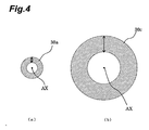
- Fig. 4 (a) and (b) is a drawing for explaining the operation of the zoom lens on the secondary light source of annular shape.
- the secondary light source 30a of annular shape is formed in the standard state, and when the focal length of the zoom lens 7 is increased from the minimum to a predetermined value, the secondary light source 30a is changed to a secondary light source 30c of annular shape with the overall shape similarly enlarged as shown in Fig. 4 (b).
- the width and size (outside diameter) of the annular secondary light source both vary without change in the annular ratio thereof, by the operation of the zoom lens 7.
- the afocal lens (relay optical system) 4, the conical axicon system 6, and the zoom lens (magnification-varying optical system) 7 constitute a shaping optical system disposed in the optical path between the diffractive optical element 3 and the micro fly's eye lens (optical integrator) 8 and adapted for changing the size and shape of the secondary light source (substantial surface illuminant) formed on the illumination pupil plane.
- the diffractive optical element for quadrupole illumination has the following function: when a parallel light beam having a rectangular cross section is incident thereto, it forms a light intensity distribution of quadrupole shape in its far field. Therefore, light beams having passed through the diffractive optical element for quadrupole illumination form an illumination field of quadrupole shape consisting of four circular illumination fields around the optical axis AX, for example, on the entrance surface of the micro fly's eye lens 8. As a result, a secondary light source of the same quadrupole shape as the illumination field formed on the entrance surface is also formed on or near the rear focal plane of the micro fly's eye lens 8.
- the diffractive optical element for circular illumination has the following function: when a parallel light beam having a rectangular cross section is incident thereto, it forms a light intensity distribution of circular shape in its far field. Therefore, a light beam having passed through the diffractive optical element for circular illumination forms an illumination field of circular shape centered on the optical axis AX, for example, on the entrance surface of the micro fly's eye lens 8. As a result, the secondary light source of the same circular shape as the illumination field formed on the entrance surface is also formed on or near the rear focal plane of the micro fly's eye lens 8.
- the zero-order light (unwanted light) arising from the diffractive optical element 3, for example, because of manufacture error or the like is focused in the central region of the entrance surface of the micro fly's eye lens 8 (portion near the optical axis AX) to form the surface illuminant in the relatively small size but with the high luminance in the center of the annular secondary light source, thereby failing to achieve desired annular illumination.
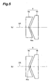
- a diffusion region 6aa for substantially scattering incident light is provided in the central region of the concave conical refracting surface of the first prism member 6a in the conical axicon system 6, as shown in Fig. 5 (a).
- the diffusion region 6aa on the first prism member 6a is located at a position substantially in the relation of Fourier transform with the diffractive optical element 3. Therefore, the zero-order light arising from the diffractive optical element 3 is focused approximately at a point by the front unit 4a of the afocal lens 4 to impinge on the diffusion region 6aa on the first prism member 6a.
- the zero-order light impinging on the diffusion region 6aa is subject to the scattering operation thereof to be guided to the outside of the illumination light path.
- the diffusion region 6aa formed in the central region of the concave conical refracting surface of the first prism member 6a is disposed at or near the pupil position of the afocal lens 4 (generally, at a position substantially in the relation of Fourier transform with the diffractive optical element 3 in the optical path of the shaping optical system (4, 6, 7)), and constitutes a preventing device for preventing the zero-order light from the diffractive optical element 3 from traveling along the illumination light path.
- the zero-order light arising from the diffractive optical element 3 is blocked by the scattering operation of the diffusion region 6aa as the preventing device and desired annular illumination is accomplished without forming a surface illuminant with a high luminance in the center of the annular secondary light source.
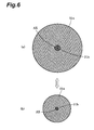
- a small shadow part 31 b as shown in Fig. 6 (a) and (b), with a light intensity substantially lower than that in the region around it is formed in the central region of the secondary light source 31 a of circular shape (portion near the optical axis AX) because of influence of the diffusion region 6aa formed in the central region of the concave conical refracting surface of the first prism member 6a.
- the overall shape of the circular secondary light source 31a including the shadow part 31b in the central region is similarly reduced or enlarged by operation of the zoom lens 7.
- the ratio of the outside diameter of the circular secondary light source 31a to the outside diameter of the shadow part 31b is constant both in large- ⁇ circular illumination of Fig. 6 (a) using a relatively large secondary light source of circular shape and in small- ⁇ circular illumination of Fig. 6 (b) using a relatively small secondary light source of circular shape.
- the influence of the shadow part 31 b on the circular secondary light source 31a is constant, independent of variation in the ⁇ -value in the circular illumination.
- almost desired circular illumination with an arbitrary ⁇ -value can be accomplished with little influence of the diffusion region 6aa formed in the central region of the concave conical refracting surface of the first prism member 6a.
- the illumination optical apparatus (1-11) of the present embodiment is able to accomplish desired annular illumination, almost desired circular illumination with an arbitrary ⁇ -value, and so on, without substantial influence of the zero-order light from the diffractive optical element 3.
- the exposure apparatus (1-PL) of the present embodiment is able to perform good exposure under an appropriate illumination condition realized according to a pattern characteristic of mask M, because it uses the illumination optical apparatus (1-11) achieving the desired annular illumination and circular illumination without substantial influence of the zero-order light from the diffractive optical element 3.
- the diffusion region 6aa as the preventing device is provided in the central region of the concave circular refracting surface of the first prism member 6a in the conical axicon system 6.
- a diffusion region 6ba for substantially scattering incident light in the central region of the convex conical refracting surface of the second prism member 6b (portion near the optical axis AX) in the conical axicon system 6.
- a preferred configuration to minimize the size of the diffusion region 6aa, so as to minimize the size of the shadow part 31 b in the circular secondary light source 31a is one wherein the diffusion region 6aa is placed on the first prism member 6a, the first prism member 6a is fixed along the optical path AX, and the second prism member 6b is moved along the optical axis AX.
- the optical member located in the optical path between the preventing device and the diffractive optical element 3 is preferably fixed in order to minimize the size of the shadow part 31b.
- the diffusion region 6aa for substantially scattering the zero-order light incident thereto is used as the preventing device for preventing the zero-order light from the diffractive optical element 3 from traveling along the illumination light path.
- a shield region for substantially blocking the zero-order light incident thereto is also possible to use as the preventing device.
- a potential configuration is such that a shield region consisting of a light-shielding thin film, e.g., chromium film is formed in the central region of the concave conical refracting surface of the first prism member 6a (or in the central region of the convex conical refracting surface of the second prism member 6b).
- the diffusion region 6aa as the preventing device is provide on the first prism member 6a forming the conical axicon system 6.
- a diffusion region (or shield region) 12a as a preventing device is provided in a central region of a plane-parallel plate 12 (portion near the optical axis AX) located at or near the pupil position of the afocal lens 4 (at a position substantially in the relation of Fourier transform with the diffractive optical element 3).
- a relatively small diffusion member (or shield member) 13 centered on the optical axis AX is provided at or near the pupil position of the afocal lens 4 (at a position substantially in the relation of Fourier transform with the diffractive optical element 3).
- a preferred configuration is such that the diffusion member (or shield member) 13 is stably supported by means of a plurality of rod members 13a (three members in Fig. 7) as thin as possible, so as not to substantially block passage of required rays contributing to illumination.
- the preventing device is provided on the first prism member 6a forming the conical axicon system 6.
- plural types of preventing devices different in the size of the shield region (or the diffusion region) may be arranged as replaceable, for example as shown in Fig. 8, at a position near the entrance surface of the micro fly's eye lens 8.
- Fig. 8 is a drawing schematically showing a configuration of a modification example wherein plural types of preventing devices are arranged as replaceable, in which members with equivalent functionality are denoted by the same reference symbols as in Fig. 1.
- members with equivalent functionality are denoted by the same reference symbols as in Fig. 1.
- the below will describe only a different configuration from the embodiment shown in Fig. 1.
- a first shield member 51 as a preventing device is disposed at a position near the entrance surface of the micro fly's eye lens 8 (which is a position substantially in the relation of Fourier transform with the diffractive optical element 3, where the zero-order light from the diffractive optical element 3 is focused).
- this first shield member 51 is composed of a shield region 51a, an outer frame 51 b, and rod members 51 c supporting the shield region 51a, and is arranged to be replaceable with a second shield member 52 having a shield region 52a of a different size.
- the first shield member 51 shown in Fig. 9 (a) is positioned in the illumination light path in order to accomplish large- ⁇ illumination using a relatively large, circular, secondary light source
- the second shield member 52 shown in Fig. 9 (b) is positioned in the illumination light path in order to accomplish small- ⁇ illumination using a relatively small, circular, secondary light source.
- this configuration limits the region where the shield region 52a shields the second light source, to an extremely small area even in the case of small ⁇ -illumination using the relatively small, circular, secondary light source, whereby almost predetermined circular illumination with an arbitrary ⁇ -value can be accomplished with little influence of the shield region 52a.
- the micro fly's eye lens 8 was used as an optical integrator for uniformizing the illuminance on the surface to be illuminated, but, without having to be limited to it, an internal reflection type rod integrator 81 may be used as an optical integrator, for example, as shown in Fig. 10.
- Fig. 10 is a drawing schematically showing a configuration of a modification example where the rod integrator of the internal reflection type is used as an optical integrator, in which members with similar functionality are denoted by the same reference symbols as in the examples of Figs. 1 and 8.
- members with similar functionality are denoted by the same reference symbols as in the examples of Figs. 1 and 8.
- the below will describe only a different configuration from the examples of Figs. 1 and 8.
- the afocal lens 4 is disposed in the optical path between the diffractive optical element 3 and the rod integrator 81.
- the afocal lens 4 is composed of a front unit having lenses (or lens units) 4a, 4b, and a rear unit having a lens unit 4c.
- the rear focal position of the lenses (lens units) 4a, 4b agrees approximately with the front focal position of the lens unit 4c, and the lenses (lens units) 4a, 4b, 4c as a whole constitute an afocal optical system.
- the conical axicon system 6 having the first prism member 6a and the second prism member 6b is disposed in the optical path between the lenses (lens units) 4a, 4b.
- the first shield member 51 as the preventing device is also disposed near the rear focal position of the lenses (lens units) 4a, 4b (which is a position substantially in the relation of Fourier transform with the diffractive optical element 3, where the zero-order light from the diffractive optical element 3 is focused).
- This first shield member 51 is arranged as replaceable with the second shield member 52 having the shield region 52a of the different size. Thanks to this configuration, the modification example of Fig.
- the shield region 52a shields the secondary light source, to an extremely small area even in the case of small- ⁇ illumination using the relatively small, circular, secondary light source, and is thus able to accomplish almost predetermined circular illumination with an arbitrary ⁇ -value, with little influence of the shield region 52a.
- the exposure apparatus of the foregoing embodiment can be used to manufacture micro devices (semiconductor devices, image pickup devices, liquid-crystal display devices, thin-film magnetic heads, etc.) by illuminating a mask (reticle) by the illumination optical apparatus (illumination step) and projecting a pattern to be transferred, formed in the mask, onto a photosensitive substrate with the projection optical system (exposure step).
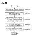
- a technique of forming a predetermined circuit pattern in a wafer or the like as a photosensitive substrate with the exposure apparatus of the foregoing embodiment to obtain semiconductor devices as micro devices will be described below with reference to the flowchart of Fig. 11.
- the first step 301 in Fig. 11 is to deposit a metal film on each wafer in one lot.
- the next step 302 is to apply a photoresist onto the metal film on each wafer in the lot.
- the subsequent step 303 is to sequentially transfer an image of a pattern on the mask into each shot area on each wafer in the lot through the projection optical system, using the exposure apparatus of the foregoing embodiment.
- the subsequent step 304 is to perform development of the photoresist on each wafer in the lot and the subsequent step 305 is to perform etching on each wafer in the lot, using the resist pattern as a mask, and thereby to form a circuit pattern corresponding to the pattern on the mask, in each shot area on each wafer.
- Subsequent steps include formation of circuit patterns in upper layers, and others, thereby manufacturing devices such as semiconductor devices.
- the above-described semiconductor device manufacturing method permits us to obtain semiconductor devices with extremely fine circuit patterns at high throughput.
- a pattern forming step 401 is to execute a so-called photolithography step to transfer a pattern of a mask onto a photosensitive substrate (glass substrate coated with a resist, or the like) with the exposure apparatus of the foregoing embodiment.
- This photolithography step results in forming the predetermined pattern including a number of electrodes and others on the photosensitive substrate.
- steps such as development, etching, and resist removal, whereby a predetermined pattern is formed on the substrate.
- the process shifts to the next color filter forming step 402.
- the next color filter forming step 402 is to form a color filter in which a number of sets of three dots corresponding to R (Red), G (Green), and B (Blue) are arrayed in a matrix pattern, or in which sets of three stripe filters of R, G, and B are arrayed as a plurality of lines along the horizontal scan line direction.
- a cell assembling step 403 is carried out.
- the cell assembling step 403 is to assemble a liquid crystal panel (liquid crystal cell), using the substrate with the predetermined pattern obtained in the pattern forming step 401, the color filter obtained in the color filter forming step 402, and so on.
- a liquid crystal is poured into between the substrate with the predetermined pattern obtained in the pattern forming step 401 and the color filter obtained in the color filter forming step 402, to manufacture a liquid crystal panel (liquid crystal cell).
- the subsequent module assembling step 404 is to install each of components such as an electric circuit, a backlight, etc. for display operation of the assembled liquid crystal panel (liquid crystal cell) to complete the liquid-crystal display device.
- the above-described method of manufacturing the liquid-crystal display device permits us to obtain the liquid-crystal display device with an extremely fine circuit pattern at high throughput.
- the exposure light was the ArF excimer laser light (wavelength: 193 nm), but, without having to be limited to it, the present invention is also applicable to other appropriate laser light sources, e.g., a KrF excimer laser light source for supplying light having the wavelength of 248 nm and an F 2 laser light source for supplying a laser beam having the wavelength of 157 nm.
- a KrF excimer laser light source for supplying light having the wavelength of 248 nm
- an F 2 laser light source for supplying a laser beam having the wavelength of 157 nm.
- the foregoing embodiment described the application of the present invention to the illumination optical apparatus for illuminating the mask in the exposure apparatus, but, without having to be limited to it, the present invention is also applicable to ordinary illumination optical apparatus for illuminating other surfaces to be illuminated, except for the mask with the light beam from the light source.
- the technique of filling the liquid in the optical path between the projection optical system and the photosensitive substrate can be one selected from the method of locally filling the space with the liquid as disclosed in International Publication WO99/49504 , the method of moving a stage holding a substrate as an exposed object, in a liquid bath as disclosed in Japanese Patent Application Laid-open No. 6-124873 , the method of forming a liquid bath of a predetermined depth on a stage and holding a substrate in the liquid bath as disclosed in Japanese Patent Application Laid-open No. 10-303114 , and so on.
- the liquid is preferably one that is transparent to the exposure light, that has the refractive index as high as possible, and that is stable against the projection optical system and the photoresist laid on the surface of the substrate; for example, where the KrF excimer laser light or the ArF excimer laser light is used as the exposure light, the liquid can be pure water or deionized water. Where the exposure light is the F 2 laser light, the liquid can be a fluorine-based liquid, for example, such as fluorine oil or perfluoro polyether (PFPE) capable of transmitting the F 2 laser light.
- PFPE perfluoro polyether
Landscapes
- Physics & Mathematics (AREA)
- General Physics & Mathematics (AREA)
- Optics & Photonics (AREA)
- Exposure And Positioning Against Photoresist Photosensitive Materials (AREA)
- Exposure Of Semiconductors, Excluding Electron Or Ion Beam Exposure (AREA)
- Lenses (AREA)
Abstract
Description
- The present invention relates to an illumination optical apparatus, exposure apparatus, and exposure method and, more particularly, to an illumination optical apparatus suitably applicable to exposure apparatus for manufacturing micro devices, such as semiconductor devices, image pickup devices, liquid-crystal display devices, and thin-film magnetic heads, by lithography.
- In the typical exposure apparatus of this type, a light beam emitted from a light source is guided through a fly's eye lens as an optical integrator to form a secondary light source as a substantial surface illuminant consisting of a lot of light sources. Light beams from the secondary light source are guided through an aperture stop disposed in the vicinity of the rear focal plane of the fly's eye lens, to be limited thereby, and then enter a condenser lens.
- The light beams condensed by the condenser lens illuminate a mask with a predetermined pattern therein, in a superposed manner. Light transmitted by the pattern of the mask travels through a projection optical system to be focused on a wafer. In this manner the mask pattern is projected (or transferred) onto the wafer to effect exposure thereof. The pattern formed in the mask is of high integration and a uniform illuminance distribution must be formed on the wafer in order to accurately transfer the microscopic pattern onto the wafer.
- For highly accurately transferring the microscopic pattern onto the wafer, attention is being focused on the technology of forming the secondary light source of circular shape on the rear focal plane of the fly's eye lens and changing the size thereof to vary the coherency σ of illumination (σ value = diameter of an aperture stop/pupil diameter of a projection optical system, or σ value = exit-side numerical aperture of an illumination optical system/entrance-side numerical aperture of the projection optical system). Furthermore, attention is also focused on the technology of forming the secondary light source of annular shape or quadrupole shape on the rear focal plane of the fly's eye lens to improve the depth of focus and resolving power of the projection optical system.
- The conventional exposure apparatus as described above were arranged to convert an incident light beam into a light beam of a desired sectional shape by a diffractive optical element and to guide it to the entrance surface of the fly's eye lens to accomplish normal circular illumination based on the circular secondary light source, or to accomplish modified or off-axis illumination (annular illumination or quadrupole illumination) based on the secondary light source of an annular shape or quadrupole shape. The diffractive optical element herein is so designed substantially as not to generate the zero-order light (direct light).
- It is, however, difficult to avoid occurrence of zero-order light from the diffractive optical element, for example, because of manufacture error or the like. In this case, the zero-order light arising from the diffractive optical element becomes unwanted light as focused in the central area (portion in the vicinity of the optical axis) on the entrance surface of the fly's eye lens and, for example, during annular illumination, it forms a surface illuminant in a relatively small size but with a high luminance in the center of the annular secondary light source. As a result, the unwanted surface illuminant is formed in the center of the annular secondary light source, which results in failure in accomplishment of desired annular illumination.
- The conventional technology proposes a configuration for blocking light near the optical axis (or the zero-order light from the diffractive optical element) in the vicinity of the entrance surface or the exit surface of the fly's eye lens, in order to accomplish the desired annular illumination (e.g., cf. Patent Document 1).
Patent Document 1:Japanese Patent Application Laid-open No. 2001-176766 - As described above, the conventional technology adopts the center blocking in the vicinity of the entrance surface or the exit surface of the fly's eye lens to avoid the influence of the zero-order light from the diffractive optical element, thereby achieving, the desired annular illumination. In the circular illumination, however, a relatively small dark part is formed in the center of the secondary light source because of influence of the foregoing center blocking and thus the secondary light source of annular shape is formed instead of the desired circular secondary light source.
- In the case of circular illumination using a relatively large, circular, secondary light source, i.e., in the case of large-σ circular illumination, the outside diameter of the secondary light source is much larger than that of the dark part, so that almost desired large-σ circular illumination can be accomplished with little influence of the dark part. In the case of small-σ circular illumination using a relatively small, circular, secondary light source, however, an annular secondary light source substantially different from the desired circular shape is formed because of influence of the dark part, thus failing to accomplish the desired small-σ circular illumination.
- An object of the present invention is to provide an illumination optical apparatus capable of achieving desired annular illumination, circular illumination, and so on, without substantial influence of the zero-order light from a diffractive optical element. Another object of the invention is to provide an exposure apparatus and exposure method capable of performing good exposure under an appropriate illumination condition realized according to a pattern characteristic of a mask, using an illumination optical apparatus achieving desired annular illumination, circular illumination, and so on without substantial influence of the zero-order light from a diffractive optical element.
- In order to achieve the foregoing object, a first aspect of the present invention provides an illumination optical apparatus for illuminating a surface to be illuminated, with a light beam from a light source,
the illumination optical apparatus comprising: - a diffractive optical element which converts the light beam from the light source into a light beam with a predetermined light intensity distribution;
- an optical integrator disposed in an optical path between the diffractive optical element and the surface to be illuminated;
- a shaping optical system disposed in an optical path between the diffractive optical element and the optical integrator and adapted for changing a size and shape of the substantial surface illuminant; and
- preventing means disposed at a position in the optical path between the diffractive optical element and the optical integrator, where zero-order light from the diffractive optical element is focused, and adapted for preventing the zero-order light from the diffractive optical element from traveling along an illumination light path;
- A second aspect of the present invention provides an illumination optical apparatus for illuminating a surface to be illuminated, with a light beam from a light source, the illumination optical apparatus comprising:
- a diffractive optical element which converts the light beam from the light source into a light beam with a predetermined light intensity distribution;
- an optical integrator disposed in an optical path between the diffractive optical element and the surface to be illuminated;
- a shaping optical system disposed in an optical path between the diffractive optical element and the optical integrator and adapted for changing a size and shape of the substantial surface illuminant; and
- preventing means disposed at a position where zero-order light from the diffractive optical element is focused, in an optical path of the shaping optical system, and adapted for preventing the zero-order light from the diffractive optical element from traveling along an illumination light path.
- A third aspect of the present invention provides an exposure apparatus comprising the illumination optical apparatus of the first aspect or the second aspect for illuminating a mask, and being adapted for exposure of a pattern of the mask on a photosensitive substrate.
- A fourth aspect of the present invention provides an exposure method comprising an illumination step of illuminating a mask by means of the illumination optical apparatus of the first aspect or the second aspect; and an exposure step of effecting exposure of a pattern of the mask on a photosensitive substrate.
- A fifth aspect of the present invention provides a device manufacturing method comprising: an illumination step of illuminating a mask by means of the illumination optical apparatus of the first aspect or the second aspect; an exposure step of effecting exposure of a pattern of the mask on a photosensitive substrate; and a development step of developing the photosensitive substrate subjected to the exposure in the exposure step.
- In the illumination optical apparatus of the present invention, the preventing means for preventing the zero-order light from the diffractive optical element from traveling along the illumination light path is disposed at a position substantially in the relation of Fourier transform with the diffractive optical element, in the optical path of the shaping optical system for changing the size and shape of the substantial surface illuminant formed on the illumination pupil plane of the illumination optical apparatus. As a result, desired annular illumination and circular illumination is accomplished without substantial influence of the zero-order light from the diffractive optical element, by the operation of the preventing means.
- Consequently, since the exposure apparatus and exposure method of the present invention use the illumination optical apparatus achieving the desired annular illumination and circular illumination without substantial influence of the zero-order light from the diffractive optical element, they are able to perform good exposure under an appropriate illumination condition realized according to a pattern characteristic of the mask and are thus able to manufacture good devices at high throughput.
-
- Fig. 1 is a drawing schematically showing a configuration of an exposure apparatus according to an embodiment of the present invention.
- Fig. 2 is a drawing schematically showing a configuration of a conical axicon system in Fig. 1.
- Fig. 3 is a drawing for explaining the operation of the conical axicon system on a secondary light source of an annular shape.
- Fig. 4 is a drawing for explaining the operation of a zoom lens on a secondary light source of an annular shape.
- Fig. 5 is a drawing schematically showing a configuration of a preventing device being a characteristic configuration of the embodiment.
- Fig. 6 is a drawing schematically showing a secondary light source formed in circular illumination in the embodiment.
- Fig. 7 is a drawing schematically showing a modification example of the preventing device.
- Fig. 8 is a drawing schematically showing a configuration of a modification example in which plural types of preventing devices are arranged as replaceable.
- Fig. 9 is a drawing schematically showing configurations of shield members as the preventing devices in Fig. 8.
- Fig. 10 is a drawing schematically showing a configuration of a modification example using an internal reflection type rod integrator as an optical integrator.
- Fig. 11 is a flowchart of a technique of manufacturing semiconductor devices as micro devices.
- Fig. 12 is a flowchart of a technique of manufacturing a liquid-crystal display element as a micro device.
- Embodiments of the present invention will be described on the basis of the accompanying drawings. Fig. 1 is a drawing schematically showing a configuration of an exposure apparatus according to an embodiment of the present invention. In Fig. 1, the Z-axis is set along a direction of a normal to a wafer W being a photosensitive substrate, the Y-axis along a direction parallel to the page of Fig. 1 in the surface of wafer W, and the X-axis along a direction perpendicular to the page of Fig. 1 in the surface of wafer W.
- With reference to Fig. 1, the exposure apparatus of the present embodiment is provided with a
light source 1 for supplying exposure light (illumination light). Thelight source 1 to be used can be, for example, an ArF excimer laser light source for supplying light of the wavelength of 193 nm. A nearly parallel light beam emitted from thelight source 1 travels via arelay lens system 2 and a diffractiveoptical element 3 for annular illumination to enter anafocal lens 4. Therelay lens system 2 has a function of converting the nearly parallel light beam from thelight source 1 into a nearly parallel light beam having a cross section of a predetermined rectangular shape and guiding it to the diffractiveoptical element 3. - The
afocal lens 4 is an afocal system (afocal optic) so set that the front focal position thereof is approximately coincident with the position of the diffractiveoptical element 3 and that the rear focal position thereof is approximately coincident with a position of apredetermined plane 5 indicated by a dashed line in the drawing. On the other hand, the diffractiveoptical element 3 is made by forming steps with a pitch approximately equal to the wavelength of the exposure light (illumination light) in a substrate, and functions to diffract an incident light beam at desired angles. Specifically, the diffractiveoptical element 3 for annular illumination has the following function: when a parallel light beam with a rectangular cross section is incident to the diffractiveoptical element 3, it forms a light intensity distribution of an annular shape in its far field (or Fraunhofer diffraction region). - Therefore, the nearly parallel light beam incident to the diffractive
optical element 3 as a light beam conversion element forms an annular light intensity distribution on the pupil plane of theafocal lens 4 as a relay optical system and thereafter is exited as a nearly parallel light beam from theafocal lens 4. Aconical axicon system 6 is disposed in the optical path between afront lens unit 4a and arear lens unit 4b of theafocal lens 4 and at or near the pupil plane thereof, and the detailed configuration and operation thereof will be described later. For simplification of description, the basic configuration and operation will be described below, while ignoring the operation of theconical axicon system 6. - The light beam having passed through the
afocal lens 4 travels through azoom lens 7 for variation of σ-value to enter a micro fly's eye lens (or fly's eye lens) 8 as an optical integrator. The micro fly'seye lens 8 is an optical element consisting of a number of micro-lenses with a positive refractive power arranged vertically and horizontally, and densely. In general, a micro fly's eye lens is made, for example, by forming a micro-lens group in a plane-parallel plate by etching. - Each of the micro-lenses constituting the micro fly's eye lens is smaller than each of lens elements constituting a fly's eye lens. The micro fly's eye lens is a lens wherein a number of micro-lenses (micro-refracting surfaces) are integrally formed without being isolated from each other, different from the fly's eye lens consisting of lens elements isolated from each other. However, the micro fly's eye lens is an optical integrator of the same wavefront splitting type as the fly's eye lens in that the lens elements with a positive refractive power are arranged vertically and horizontally.
- The
predetermined plane 5 is located near the front focal position of thezoom lens 7 and the entrance surface of the micro fly'seye lens 8 is located near the rear focal position of thezoom lens 7. In other words, thezoom lens 7 functions to arrange thepredetermined plane 5 and the entrance surface of the micro fly'seye lens 8 substantially in the relation of Fourier transform and, eventually, to arrange the pupil plane of theafocal lens 4 and the entrance surface of the micro fly'seye lens 8 substantially optically conjugate with each other. - Therefore, for example, an annular illumination field centered on the optical axis AX is formed on the entrance surface of the micro fly's
eye lens 8, as on the pupil plane of theafocal lens 4. The overall shape of this annular illumination field varies similarly depending upon the focal length of thezoom lens 7 as described below. Each micro-lens forming the micro fly'seye lens 8 has a rectangular cross section similar to a shape of an illumination field to be formed on a mask M (and, eventually, similar to a shape of an exposure region to be formed on a wafer W). - The light beam incident to the micro fly's
eye lens 8 is two-dimensionally split by the multiple micro-lenses to form a secondary light source having much the same light intensity distribution as the illumination field formed by the incident light beam, i.e., a secondary light source having a substantial surface illuminant of an annular shape centered on the optical axis AX, on or near the rear focal plane of the micro fly's eye lens 8 (and on the illumination pupil plane eventually). Light beams from the secondary light source formed on or near the rear focal plane of the micro fly'seye lens 8 travel through a condenseroptical system 9 and then illuminate a mask blind 10 in a superposed manner. - In this manner, a rectangular illumination field according to the shape and focal length of each micros-lens forming the micro fly's
eye lens 8 is formed on themask blind 10 as an illumination field stop. The light beam having passed through a rectangular aperture (light transmitting portion) of themask blind 10 is subject to focusing operation of an imagingoptical system 11 and then illuminates the mask M with the predetermined pattern therein, in a superposed manner. Namely, the imagingoptical system 11 forms an image of the rectangular aperture of themask blind 10 on the mask M. - The light beam transmitted by the pattern of the mask M held on a mask stage MS travels through a projection optical system PL to form an image of the mask pattern on the wafer W (a photosensitive substrate) held on a wafer stage WS. While the wafer stage WS is two-dimensionally driven and controlled in the plane (XY plane) perpendicular to the optical axis AX of the projection optical system PL, i.e., while the wafer W is two-dimensionally driven and controlled, one-shot exposure or scan exposure is effected to sequentially project the pattern of the mask M into each of exposure regions on the wafer W.
- Fig. 2 is a drawing schematically showing the configuration of the conical axicon system disposed in the optical path between the front lens unit and the rear lens unit of the afocal lens. The
conical axicon system 6 is composed of afirst prism member 6a a planar surface of which faces the light source side and a refracting surface of a concave conical shape of which faces the mask side, and asecond prism member 6b a planar surface of which faces the mask side and a refracting surface of a convex conical shape of which faces the light source side, in order from the light source side. - Then the refracting surface of the concave conical shape of the
first prism member 6a and the refracting surface of the convex conical shape of thesecond prism member 6b are formed in such complementary shapes as to be able to butt each other. At least one of thefirst prism member 6a and thesecond prism member 6b is arranged to be movable along the optical axis AX to vary the distance between the refracting surface of the concave conical shape of thefirst prism member 6a and the refracting surface of the convex conical shape of thesecond prism member 6b. - In a state in which the refracting surface of the concave conical shape of the
first prism member 6a butts on the refracting surface of the convex conical shape of thesecond prism member 6b, theconical axicon system 6 functions as a plane-parallel plate and has no effect on the secondary light source of annular shape formed. However, when the refracting surface of the concave conical shape of thefirst prism member 6a is located apart from the refracting surface of the convex conical shape of thesecond prism member 6b, theconical axicon system 6 functions a so-called light beam expander. Therefore, an angle of the incident light beam to thepredetermined plane 5 varies with change in the distance in theconical axicon system 6. - Fig. 3 (a) and (b) is a drawing for explaining the operation of the conical axicon system on the secondary light source of annular shape. With reference to Fig. 3 (a), the smallest secondary
light source 30a of annular shape is formed in a state in which the distance in theconical axicon system 6 is zero and in which the focal length of thezoom lens 7 is set at a minimum (which will be referred to hereinafter as "standard state"), and when the distance in theconical axicon system 6 is increased from zero to a predetermined value, the secondarylight source 30a is changed to a secondarylight source 30b with the outside diameter and the inside diameter both increased, without change in its width (half of the difference between the outside diameter and the inside diameter: as indicated by arrows in the drawing) as shown in Fig. 3 (b). In other words, the annular ratio (inside diameter/outside diameter) and the size (outside diameter) both vary without change in the width of the annular secondary light source, by the operation of theconical axicon system 6. - Fig. 4 (a) and (b) is a drawing for explaining the operation of the zoom lens on the secondary light source of annular shape. With reference to Fig. 4 (a), the secondary
light source 30a of annular shape is formed in the standard state, and when the focal length of thezoom lens 7 is increased from the minimum to a predetermined value, the secondarylight source 30a is changed to a secondarylight source 30c of annular shape with the overall shape similarly enlarged as shown in Fig. 4 (b). In other words, the width and size (outside diameter) of the annular secondary light source both vary without change in the annular ratio thereof, by the operation of thezoom lens 7. - As described above, the afocal lens (relay optical system) 4, the
conical axicon system 6, and the zoom lens (magnification-varying optical system) 7 constitute a shaping optical system disposed in the optical path between the diffractiveoptical element 3 and the micro fly's eye lens (optical integrator) 8 and adapted for changing the size and shape of the secondary light source (substantial surface illuminant) formed on the illumination pupil plane. - When a diffractive optical element for quadrupole illumination (not shown) is set in the illumination light path, instead of the diffractive
optical element 3 for annular illumination, it can effect quadrupole illumination. The diffractive optical element for quadrupole illumination has the following function: when a parallel light beam having a rectangular cross section is incident thereto, it forms a light intensity distribution of quadrupole shape in its far field. Therefore, light beams having passed through the diffractive optical element for quadrupole illumination form an illumination field of quadrupole shape consisting of four circular illumination fields around the optical axis AX, for example, on the entrance surface of the micro fly'seye lens 8. As a result, a secondary light source of the same quadrupole shape as the illumination field formed on the entrance surface is also formed on or near the rear focal plane of the micro fly'seye lens 8. - When a diffractive optical element for circular illumination (not shown) is set in the illumination light path, instead of the diffractive
optical element 3 for annular illumination, it can effect normal circular illumination. The diffractive optical element for circular illumination has the following function: when a parallel light beam having a rectangular cross section is incident thereto, it forms a light intensity distribution of circular shape in its far field. Therefore, a light beam having passed through the diffractive optical element for circular illumination forms an illumination field of circular shape centered on the optical axis AX, for example, on the entrance surface of the micro fly'seye lens 8. As a result, the secondary light source of the same circular shape as the illumination field formed on the entrance surface is also formed on or near the rear focal plane of the micro fly'seye lens 8. - Furthermore, when another diffractive optical element for multi-pole illumination (not shown) is set in the illumination light path, instead of the diffractive
optical element 3 for annular illumination, it is feasible to accomplish one of various multi-pole illuminations (dipole illumination, octupole illumination, etc.). Similarly, when a diffractive optical element with an appropriate characteristic (not shown) is set in the illumination light path, instead of the diffractiveoptical element 3 for annular illumination, it becomes feasible to accomplish one of off-axis or modified illuminations of various forms. - In the conventional technology, as described above, the zero-order light (unwanted light) arising from the diffractive
optical element 3, for example, because of manufacture error or the like is focused in the central region of the entrance surface of the micro fly's eye lens 8 (portion near the optical axis AX) to form the surface illuminant in the relatively small size but with the high luminance in the center of the annular secondary light source, thereby failing to achieve desired annular illumination. In the present embodiment, therefore, a diffusion region 6aa for substantially scattering incident light is provided in the central region of the concave conical refracting surface of thefirst prism member 6a in theconical axicon system 6, as shown in Fig. 5 (a). - Since the
conical axicon system 6 is disposed at or near the pupil position of theafocal lens 4 as described above, the diffusion region 6aa on thefirst prism member 6a is located at a position substantially in the relation of Fourier transform with the diffractiveoptical element 3. Therefore, the zero-order light arising from the diffractiveoptical element 3 is focused approximately at a point by thefront unit 4a of theafocal lens 4 to impinge on the diffusion region 6aa on thefirst prism member 6a. The zero-order light impinging on the diffusion region 6aa is subject to the scattering operation thereof to be guided to the outside of the illumination light path. - In this way, the diffusion region 6aa formed in the central region of the concave conical refracting surface of the
first prism member 6a is disposed at or near the pupil position of the afocal lens 4 (generally, at a position substantially in the relation of Fourier transform with the diffractiveoptical element 3 in the optical path of the shaping optical system (4, 6, 7)), and constitutes a preventing device for preventing the zero-order light from the diffractiveoptical element 3 from traveling along the illumination light path. As a result, the zero-order light arising from the diffractiveoptical element 3 is blocked by the scattering operation of the diffusion region 6aa as the preventing device and desired annular illumination is accomplished without forming a surface illuminant with a high luminance in the center of the annular secondary light source. - On the other hand, in circular illumination accomplished while the refracting surface of the
first prism member 6a is kept in contact with the refracting surface of thesecond prism member 6b, asmall shadow part 31 b, as shown in Fig. 6 (a) and (b), with a light intensity substantially lower than that in the region around it is formed in the central region of the secondarylight source 31 a of circular shape (portion near the optical axis AX) because of influence of the diffusion region 6aa formed in the central region of the concave conical refracting surface of thefirst prism member 6a. The overall shape of the circular secondarylight source 31a including theshadow part 31b in the central region is similarly reduced or enlarged by operation of thezoom lens 7. - Consequently, the ratio of the outside diameter of the circular secondary
light source 31a to the outside diameter of theshadow part 31b is constant both in large-σ circular illumination of Fig. 6 (a) using a relatively large secondary light source of circular shape and in small-σ circular illumination of Fig. 6 (b) using a relatively small secondary light source of circular shape. In other words, the influence of theshadow part 31 b on the circular secondarylight source 31a is constant, independent of variation in the σ-value in the circular illumination. As a result, almost desired circular illumination with an arbitrary σ-value can be accomplished with little influence of the diffusion region 6aa formed in the central region of the concave conical refracting surface of thefirst prism member 6a. - In this manner, the illumination optical apparatus (1-11) of the present embodiment is able to accomplish desired annular illumination, almost desired circular illumination with an arbitrary σ-value, and so on, without substantial influence of the zero-order light from the diffractive
optical element 3. Accordingly, the exposure apparatus (1-PL) of the present embodiment is able to perform good exposure under an appropriate illumination condition realized according to a pattern characteristic of mask M, because it uses the illumination optical apparatus (1-11) achieving the desired annular illumination and circular illumination without substantial influence of the zero-order light from the diffractiveoptical element 3. - In passing, if the zero-order light from the diffractive
optical element 3 is blocked in the optical path behind the micro fly's eye lens 8 (on the mask side thereof), uniformity will become more likely to degrade in the illuminance distribution on the mask M (and thus on the wafer W) as a surface to be illuminated. Similarly, if the zero-order light from the diffractiveoptical element 3 is blocked near the entrance surface of the micro fly'seye lens 8, uniformity will also become more likely to degrade in the illuminance distribution on the surface to be illuminated. - In the above-described embodiment the diffusion region 6aa as the preventing device is provided in the central region of the concave circular refracting surface of the
first prism member 6a in theconical axicon system 6. However, without having to be limited to it, it is also possible, as shown in Fig. 5 (b), to locate a diffusion region 6ba for substantially scattering incident light, in the central region of the convex conical refracting surface of thesecond prism member 6b (portion near the optical axis AX) in theconical axicon system 6. However, a preferred configuration to minimize the size of the diffusion region 6aa, so as to minimize the size of theshadow part 31 b in the circular secondarylight source 31a, is one wherein the diffusion region 6aa is placed on thefirst prism member 6a, thefirst prism member 6a is fixed along the optical path AX, and thesecond prism member 6b is moved along the optical axis AX. In other words, the optical member located in the optical path between the preventing device and the diffractiveoptical element 3 is preferably fixed in order to minimize the size of theshadow part 31b. - In the foregoing embodiment the diffusion region 6aa for substantially scattering the zero-order light incident thereto is used as the preventing device for preventing the zero-order light from the diffractive
optical element 3 from traveling along the illumination light path. However, without having to be limited to it, it is also possible to use a shield region for substantially blocking the zero-order light incident thereto, as the preventing device. In this case, a potential configuration is such that a shield region consisting of a light-shielding thin film, e.g., chromium film is formed in the central region of the concave conical refracting surface of thefirst prism member 6a (or in the central region of the convex conical refracting surface of thesecond prism member 6b). - In this connection, if the central parts of the refracting surfaces of the
prisms prism members prism members - In the foregoing embodiment the diffusion region 6aa as the preventing device is provide on the
first prism member 6a forming theconical axicon system 6. However, without having to be limited to it, for example in configurations without the conical axicon system, it is also possible, as shown in Fig. 7 (a), to adopt a modification example wherein a diffusion region (or shield region) 12a as a preventing device is provided in a central region of a plane-parallel plate 12 (portion near the optical axis AX) located at or near the pupil position of the afocal lens 4 (at a position substantially in the relation of Fourier transform with the diffractive optical element 3). - Similarly, as shown in Fig. 7 (b), it is also possible to adopt a modification example wherein a relatively small diffusion member (or shield member) 13 centered on the optical axis AX is provided at or near the pupil position of the afocal lens 4 (at a position substantially in the relation of Fourier transform with the diffractive optical element 3). In this case, a preferred configuration is such that the diffusion member (or shield member) 13 is stably supported by means of a plurality of
rod members 13a (three members in Fig. 7) as thin as possible, so as not to substantially block passage of required rays contributing to illumination. - In the foregoing embodiment the preventing device is provided on the
first prism member 6a forming theconical axicon system 6. However, without having to be limited to it, plural types of preventing devices different in the size of the shield region (or the diffusion region) may be arranged as replaceable, for example as shown in Fig. 8, at a position near the entrance surface of the micro fly'seye lens 8. - Fig. 8 is a drawing schematically showing a configuration of a modification example wherein plural types of preventing devices are arranged as replaceable, in which members with equivalent functionality are denoted by the same reference symbols as in Fig. 1. For simplifying the description, the below will describe only a different configuration from the embodiment shown in Fig. 1.
- In Fig. 8, a
first shield member 51 as a preventing device is disposed at a position near the entrance surface of the micro fly's eye lens 8 (which is a position substantially in the relation of Fourier transform with the diffractiveoptical element 3, where the zero-order light from the diffractiveoptical element 3 is focused). As shown in Fig. 9 (a) and (b), thisfirst shield member 51 is composed of ashield region 51a, anouter frame 51 b, androd members 51 c supporting theshield region 51a, and is arranged to be replaceable with asecond shield member 52 having ashield region 52a of a different size. - In the modification example shown in Figs. 8 and 9, the
first shield member 51 shown in Fig. 9 (a) is positioned in the illumination light path in order to accomplish large-σ illumination using a relatively large, circular, secondary light source, and thesecond shield member 52 shown in Fig. 9 (b) is positioned in the illumination light path in order to accomplish small-σ illumination using a relatively small, circular, secondary light source. In consequence, this configuration limits the region where theshield region 52a shields the second light source, to an extremely small area even in the case of small σ-illumination using the relatively small, circular, secondary light source, whereby almost predetermined circular illumination with an arbitrary σ-value can be accomplished with little influence of theshield region 52a. - In the foregoing embodiment and modification examples, the micro fly's
eye lens 8 was used as an optical integrator for uniformizing the illuminance on the surface to be illuminated, but, without having to be limited to it, an internal reflectiontype rod integrator 81 may be used as an optical integrator, for example, as shown in Fig. 10. - Fig. 10 is a drawing schematically showing a configuration of a modification example where the rod integrator of the internal reflection type is used as an optical integrator, in which members with similar functionality are denoted by the same reference symbols as in the examples of Figs. 1 and 8. For simplifying the description, the below will describe only a different configuration from the examples of Figs. 1 and 8.
- In Fig. 10, the
afocal lens 4 is disposed in the optical path between the diffractiveoptical element 3 and therod integrator 81. In the modification example of Fig. 10, theafocal lens 4 is composed of a front unit having lenses (or lens units) 4a, 4b, and a rear unit having alens unit 4c. In this connection, the rear focal position of the lenses (lens units) 4a, 4b agrees approximately with the front focal position of thelens unit 4c, and the lenses (lens units) 4a, 4b, 4c as a whole constitute an afocal optical system. Theconical axicon system 6 having thefirst prism member 6a and thesecond prism member 6b is disposed in the optical path between the lenses (lens units) 4a, 4b. - Here the function of changing the size while keeping the width of the annular secondary light source constant by change of the distance between the
prism members conical axicon system 6 is much the same as in the foregoing embodiment. In the modification example of Fig. 10, while the rear focal position of the lenses (lens units) 4a, 4b is kept approximately constant, the focal length thereof is changed by movement of the lenses (lens units) 4a, 4b in the optical-axis direction. The combination of the internal reflectiontype rod integrator 81 with thecondenser lens unit 4c shown in Fig. 10 corresponds to the combination of the micro fly'seye lens 8 with the condenseroptical system 9 in the aforementioned embodiment. The combination of the internal reflection type rod integrator with the axicon system is disclosed in U. S. Pat. No.6,285,443 . - In the modification example of Fig. 10, as in the modification example of Fig. 8, the
first shield member 51 as the preventing device is also disposed near the rear focal position of the lenses (lens units) 4a, 4b (which is a position substantially in the relation of Fourier transform with the diffractiveoptical element 3, where the zero-order light from the diffractiveoptical element 3 is focused). Thisfirst shield member 51 is arranged as replaceable with thesecond shield member 52 having theshield region 52a of the different size. Thanks to this configuration, the modification example of Fig. 10 also limits the region where theshield region 52a shields the secondary light source, to an extremely small area even in the case of small-σ illumination using the relatively small, circular, secondary light source, and is thus able to accomplish almost predetermined circular illumination with an arbitrary σ-value, with little influence of theshield region 52a. - The modification examples shown in Figs. 8-10 used the
shield members - The exposure apparatus of the foregoing embodiment can be used to manufacture micro devices (semiconductor devices, image pickup devices, liquid-crystal display devices, thin-film magnetic heads, etc.) by illuminating a mask (reticle) by the illumination optical apparatus (illumination step) and projecting a pattern to be transferred, formed in the mask, onto a photosensitive substrate with the projection optical system (exposure step). An example of a technique of forming a predetermined circuit pattern in a wafer or the like as a photosensitive substrate with the exposure apparatus of the foregoing embodiment to obtain semiconductor devices as micro devices will be described below with reference to the flowchart of Fig. 11.
- The first step 301 in Fig. 11 is to deposit a metal film on each wafer in one lot. The next step 302 is to apply a photoresist onto the metal film on each wafer in the lot. The subsequent step 303 is to sequentially transfer an image of a pattern on the mask into each shot area on each wafer in the lot through the projection optical system, using the exposure apparatus of the foregoing embodiment. The subsequent step 304 is to perform development of the photoresist on each wafer in the lot and the subsequent step 305 is to perform etching on each wafer in the lot, using the resist pattern as a mask, and thereby to form a circuit pattern corresponding to the pattern on the mask, in each shot area on each wafer. Subsequent steps include formation of circuit patterns in upper layers, and others, thereby manufacturing devices such as semiconductor devices. The above-described semiconductor device manufacturing method permits us to obtain semiconductor devices with extremely fine circuit patterns at high throughput.
- The exposure apparatus of the foregoing embodiment can also be used to manufacture a liquid-crystal display device as a micro device by forming predetermined patterns (circuit pattern, electrode pattern, etc.) on plates (glass substrates). An example of a technique in this case will be described with reference to the flowchart of Fig. 12. In Fig. 12, a pattern forming step 401 is to execute a so-called photolithography step to transfer a pattern of a mask onto a photosensitive substrate (glass substrate coated with a resist, or the like) with the exposure apparatus of the foregoing embodiment. This photolithography step results in forming the predetermined pattern including a number of electrodes and others on the photosensitive substrate. Thereafter, the exposed substrate is subjected to each of steps such as development, etching, and resist removal, whereby a predetermined pattern is formed on the substrate. Thereafter, the process shifts to the next color filter forming step 402.
- The next color filter forming step 402 is to form a color filter in which a number of sets of three dots corresponding to R (Red), G (Green), and B (Blue) are arrayed in a matrix pattern, or in which sets of three stripe filters of R, G, and B are arrayed as a plurality of lines along the horizontal scan line direction. After completion of the color filter forming step 402, a cell assembling step 403 is carried out. The cell assembling step 403 is to assemble a liquid crystal panel (liquid crystal cell), using the substrate with the predetermined pattern obtained in the pattern forming step 401, the color filter obtained in the color filter forming step 402, and so on.
- In the cell assembling step 403, for example, a liquid crystal is poured into between the substrate with the predetermined pattern obtained in the pattern forming step 401 and the color filter obtained in the color filter forming step 402, to manufacture a liquid crystal panel (liquid crystal cell). The subsequent module assembling step 404 is to install each of components such as an electric circuit, a backlight, etc. for display operation of the assembled liquid crystal panel (liquid crystal cell) to complete the liquid-crystal display device. The above-described method of manufacturing the liquid-crystal display device permits us to obtain the liquid-crystal display device with an extremely fine circuit pattern at high throughput.
- In the foregoing embodiment, the exposure light was the ArF excimer laser light (wavelength: 193 nm), but, without having to be limited to it, the present invention is also applicable to other appropriate laser light sources, e.g., a KrF excimer laser light source for supplying light having the wavelength of 248 nm and an F2 laser light source for supplying a laser beam having the wavelength of 157 nm. Furthermore, the foregoing embodiment described the application of the present invention to the illumination optical apparatus for illuminating the mask in the exposure apparatus, but, without having to be limited to it, the present invention is also applicable to ordinary illumination optical apparatus for illuminating other surfaces to be illuminated, except for the mask with the light beam from the light source.
- In the foregoing embodiment, it is also possible to adopt a technique of filling the optical path between the projection optical system and the photosensitive substrate with a medium having the refractive index of more than 1.1 (typically, a liquid), i.e., the so-called liquid immersion method. In this case, the technique of filling the liquid in the optical path between the projection optical system and the photosensitive substrate can be one selected from the method of locally filling the space with the liquid as disclosed in
International Publication WO99/49504 Japanese Patent Application Laid-open No. 6-124873 Japanese Patent Application Laid-open No. 10-303114 - The liquid is preferably one that is transparent to the exposure light, that has the refractive index as high as possible, and that is stable against the projection optical system and the photoresist laid on the surface of the substrate; for example, where the KrF excimer laser light or the ArF excimer laser light is used as the exposure light, the liquid can be pure water or deionized water. Where the exposure light is the F2 laser light, the liquid can be a fluorine-based liquid, for example, such as fluorine oil or perfluoro polyether (PFPE) capable of transmitting the F2 laser light.
-
- 1
- light source
- 3
- diffractive optical element
- 4
- afocal lens (relay optical system)
- 6
- conical axicon system
- 6a, 6b
- prism members
- 6aa, 6ba
- diffusion regions (or shield regions)
- 7
- zoom lens (magnification-varying optical system)
- 8
- micro fly's eye lens
- 9
- condenser optical system
- 10
- mask blind
- 11
- imaging optical system
- M
- mask
- MS
- mask stage
- PL
- projection optical system
- W
- wafer
- WS
- wafer stage
Claims (14)
- An illumination optical apparatus for illuminating a surface to be illuminated, with a light beam from a light source,
the illumination optical apparatus comprising:a diffractive optical element which converts the light beam from the light source into a light beam with a predetermined light intensity distribution;an optical integrator disposed in an optical path between the diffractive optical element and the surface to be illuminated;a shaping optical system disposed in an optical path between the diffractive optical element and the optical integrator and adapted for changing a size and shape of the substantial surface illuminant; andpreventing means disposed at a position in the optical path between the diffractive optical element and the optical integrator, where zero-order light from the diffractive optical element is focused, and adapted for preventing the zero-order light from the diffractive optical element from traveling along an illumination light path;wherein the preventing means restrains influence thereof on the substantial surface illuminant even when the shaping optical system changes the size of the substantial surface illuminant. - The illumination optical apparatus according to claim 1, wherein the preventing means is disposed in an optical path of the shaping optical system.
- The illumination optical apparatus according to claim 2, wherein the shaping optical system has a relay optical system, and a magnification-varying optical system disposed in an optical path between the relay optical system and the optical integrator, and
wherein the preventing means is disposed in an optical path of the relay optical system. - The illumination optical apparatus according to any one of claims 1 to 3, wherein an optical member disposed in an optical path between the preventing means and the diffractive optical element is fixed.
- An illumination optical apparatus for illuminating a surface to be illuminated, with a light beam from a light source,
the illumination optical apparatus comprising:a diffractive optical element which converts the light beam from the light source into a light beam with a predetermined light intensity distribution;an optical integrator disposed in an optical path between the diffractive optical element and the surface to be illuminated;a shaping optical system disposed in an optical path between the diffractive optical element and the optical integrator and adapted for changing a size and shape of the substantial surface illuminant; andpreventing means disposed at a position where zero-order light from the diffractive optical element is focused, in an optical path of the shaping optical system, and adapted for preventing the zero-order light from the diffractive optical element from traveling along an illumination light path. - The illumination optical apparatus according to claim 5, wherein the shaping optical system has a relay optical system, and a magnification-varying optical system disposed in an optical path between the relay optical system and the optical integrator, and
wherein the preventing means is disposed at or near a pupil position of the relay optical system. - The illumination optical apparatus according to claim 5 or 6, wherein an optical member disposed in an optical path between the preventing means and the diffractive optical element is fixed.
- The illumination optical apparatus according to any one of claims 1 to 7, wherein the preventing means has a diffusion region for substantially scattering the zero-order light incident thereto.
- The illumination optical apparatus according to any one of claims 1 to 8, wherein the preventing means has a shield region for substantially blocking the zero-order light incident thereto.
- The illumination optical apparatus according to claim 9, further comprising: a first prism having a refracting surface of a concave cross section; and a second prism having a refracting surface of a convex cross section substantially complementary to the refracting surface of the concave cross section of the first prism, wherein the first prism and the second prism are disposed in an optical path of the relay optical system and wherein a distance between the first prism and the second prism is variable,
wherein at least one of the first prism and the second prism is provided with the diffusion region or the shield region. - The illumination optical apparatus according to claim 10, wherein the refracting surface includes a shape corresponding to a side face of a conical body centered on an optical axis of the illumination optical apparatus.
- An exposure apparatus comprising the illumination optical apparatus as defined in any one of claims 1 to 11, for illuminating a mask, the exposure apparatus being adapted for exposure of a pattern of the mask on a photosensitive substrate.
- An exposure method comprising an illumination step of illuminating a mask by means of the illumination optical apparatus as defined in any one of claims 1 to 11; and
an exposure step of effecting exposure of a pattern of the mask on a photosensitive substrate. - A device manufacturing method comprising: an illumination step of illuminating a mask by means of the illumination optical apparatus as defined in any one of claims 1 to 11; an exposure step of effecting exposure of a pattern of the mask on a photosensitive substrate; and a development step of developing the photosensitive substrate subjected to the exposure in the exposure step.
Applications Claiming Priority (2)
| Application Number | Priority Date | Filing Date | Title |
|---|---|---|---|
| JP2004303902A JP4535260B2 (en) | 2004-10-19 | 2004-10-19 | Illumination optical apparatus, exposure apparatus, and exposure method |
| PCT/JP2005/018809 WO2006043458A1 (en) | 2004-10-19 | 2005-10-12 | Lighting optical device, exposure system, and exposure method |
Publications (2)
| Publication Number | Publication Date |
|---|---|
| EP1811544A1 true EP1811544A1 (en) | 2007-07-25 |
| EP1811544A4 EP1811544A4 (en) | 2009-11-11 |
Family
ID=36202874
Family Applications (1)
| Application Number | Title | Priority Date | Filing Date |
|---|---|---|---|
| EP05793150A Withdrawn EP1811544A4 (en) | 2004-10-19 | 2005-10-12 | Lighting optical device, exposure system, and exposure method |
Country Status (6)
| Country | Link |
|---|---|
| US (1) | US8004658B2 (en) |
| EP (1) | EP1811544A4 (en) |
| JP (1) | JP4535260B2 (en) |
| KR (1) | KR101391384B1 (en) |
| CN (1) | CN100536071C (en) |
| WO (1) | WO2006043458A1 (en) |
Families Citing this family (16)
| Publication number | Priority date | Publication date | Assignee | Title |
|---|---|---|---|---|
| CN101320216B (en) * | 2008-06-18 | 2010-06-09 | 上海微电子装备有限公司 | Reshaping structure of micro-photoetching illumination iris |
| JP2010109242A (en) * | 2008-10-31 | 2010-05-13 | Canon Inc | Lighting optical system and exposure device |
| CN102495536B (en) * | 2011-12-30 | 2015-08-05 | 上海集成电路研发中心有限公司 | Litho machine |
| CN103293863B (en) * | 2012-02-24 | 2015-11-18 | 上海微电子装备有限公司 | A kind of lithography illuminating system |
| CN102937778B (en) * | 2012-11-20 | 2015-04-22 | 北京理工大学 | Method for determining matching relations among components in photoetching lighting system |
| JP2014145982A (en) * | 2013-01-30 | 2014-08-14 | Toshiba Corp | Optical device, solid-state imaging device, and method of manufacturing optical device |
| JP6168822B2 (en) * | 2013-04-04 | 2017-07-26 | オリンパス株式会社 | Pattern irradiation device |
| CN103399414B (en) * | 2013-07-22 | 2016-04-13 | 中国科学院上海光学精密机械研究所 | Eliminate the method for diffraction optical element zero-order terms and twin-image |
| CN104154495B (en) * | 2014-05-20 | 2017-12-15 | 广州市浩洋电子股份有限公司 | Mixed type optics integrator component and its optical system |
| WO2016075801A1 (en) | 2014-11-14 | 2016-05-19 | 株式会社ニコン | Shaping device and a shaping method |
| EP3219411B1 (en) | 2014-11-14 | 2020-08-19 | Nikon Corporation | Shaping device and shaping method |
| US10837617B2 (en) * | 2016-12-28 | 2020-11-17 | Dai Nippon Printing Co., Ltd. | Illumination device |
| JP7099443B2 (en) | 2017-03-31 | 2022-07-12 | 株式会社ニコン | Modeling system and modeling method |
| WO2018181344A1 (en) | 2017-03-31 | 2018-10-04 | 株式会社ニコン | Processing method and processing system |
| JP7538016B2 (en) * | 2020-11-30 | 2024-08-21 | 株式会社Screenホールディングス | Optical device and three-dimensional modeling device |
| US11300524B1 (en) * | 2021-01-06 | 2022-04-12 | Kla Corporation | Pupil-plane beam scanning for metrology |
Family Cites Families (21)
| Publication number | Priority date | Publication date | Assignee | Title |
|---|---|---|---|---|
| DE69132120T2 (en) | 1990-11-15 | 2000-09-21 | Nikon Corp., Tokio/Tokyo | Projection exposure method and apparatus |
| JP3200894B2 (en) * | 1991-03-05 | 2001-08-20 | 株式会社日立製作所 | Exposure method and apparatus |
| JPH06124873A (en) | 1992-10-09 | 1994-05-06 | Canon Inc | Immersion projection exposure system |
| DE4301574B4 (en) | 1993-01-21 | 2004-07-08 | Bernhard Prof. Dr. Lau | Device for observing the fundus, in particular an ophthalmoscope |
| US6285443B1 (en) * | 1993-12-13 | 2001-09-04 | Carl-Zeiss-Stiftung | Illuminating arrangement for a projection microlithographic apparatus |
| JPH08203801A (en) * | 1995-01-23 | 1996-08-09 | Nikon Corp | Projection exposure device |
| JP3426087B2 (en) * | 1996-06-10 | 2003-07-14 | シャープ株式会社 | Optical recording / reproducing device |
| JP3747566B2 (en) | 1997-04-23 | 2006-02-22 | 株式会社ニコン | Immersion exposure equipment |
| US6741394B1 (en) * | 1998-03-12 | 2004-05-25 | Nikon Corporation | Optical integrator, illumination optical apparatus, exposure apparatus and observation apparatus |
| JP2001338861A (en) * | 2000-05-26 | 2001-12-07 | Nikon Corp | Illumination optical device, exposure apparatus and method |
| AU2747999A (en) | 1998-03-26 | 1999-10-18 | Nikon Corporation | Projection exposure method and system |
| JP2001176766A (en) * | 1998-10-29 | 2001-06-29 | Nikon Corp | Illumination device and projection exposure device |
| US6563567B1 (en) * | 1998-12-17 | 2003-05-13 | Nikon Corporation | Method and apparatus for illuminating a surface using a projection imaging apparatus |
| DE10062579A1 (en) * | 1999-12-15 | 2001-06-21 | Nikon Corp | Optical integrator of wave front subdividing type used for photolithographic illuminating device comprises micro-optical elements arranged two-dimensionally to form light sources by subdividing wave front of falling light beam |
| JP4545874B2 (en) * | 2000-04-03 | 2010-09-15 | キヤノン株式会社 | Illumination optical system, exposure apparatus provided with the illumination optical system, and device manufacturing method using the exposure apparatus |
| JP2002158157A (en) * | 2000-11-17 | 2002-05-31 | Nikon Corp | Illumination optical apparatus, exposure apparatus, and method for manufacturing microdevice |
| EP1434092A1 (en) | 2002-12-23 | 2004-06-30 | ASML Netherlands B.V. | Lithographic apparatus, device manufacturing method, and device manufactured thereby |
| US7030966B2 (en) * | 2003-02-11 | 2006-04-18 | Asml Netherlands B.V. | Lithographic apparatus and method for optimizing an illumination source using photolithographic simulations |
| WO2005071474A2 (en) * | 2004-01-20 | 2005-08-04 | Sharp Kabushiki Kaisha | Directional backlight and multiple view display device |
| JP2005243904A (en) * | 2004-02-26 | 2005-09-08 | Nikon Corp | Illumination optical apparatus, exposure apparatus, and exposure method |
| DE102004040535A1 (en) | 2004-08-20 | 2006-02-23 | Carl Zeiss Ag | Polarization selective blazed diffractive optical element |
-
2004
- 2004-10-19 JP JP2004303902A patent/JP4535260B2/en not_active Expired - Fee Related
-
2005
- 2005-10-12 EP EP05793150A patent/EP1811544A4/en not_active Withdrawn
- 2005-10-12 WO PCT/JP2005/018809 patent/WO2006043458A1/en not_active Ceased
- 2005-10-12 US US11/665,669 patent/US8004658B2/en not_active Expired - Fee Related
- 2005-10-12 CN CNB2005800281803A patent/CN100536071C/en not_active Expired - Lifetime
- 2005-10-12 KR KR1020077002542A patent/KR101391384B1/en not_active Expired - Fee Related
Also Published As
| Publication number | Publication date |
|---|---|
| US8004658B2 (en) | 2011-08-23 |
| US20080030852A1 (en) | 2008-02-07 |
| JP4535260B2 (en) | 2010-09-01 |
| EP1811544A4 (en) | 2009-11-11 |
| HK1101221A1 (en) | 2007-10-12 |
| KR101391384B1 (en) | 2014-05-07 |
| CN100536071C (en) | 2009-09-02 |
| JP2006120675A (en) | 2006-05-11 |
| WO2006043458A1 (en) | 2006-04-27 |
| CN101006556A (en) | 2007-07-25 |
| KR20070057141A (en) | 2007-06-04 |
Similar Documents
| Publication | Publication Date | Title |
|---|---|---|
| JP5500454B2 (en) | Optical integrator, illumination optical apparatus, exposure apparatus, exposure method, and device manufacturing method | |
| US8462317B2 (en) | Illumination optical system, exposure apparatus, and device manufacturing method | |
| JP4693088B2 (en) | Illumination optical apparatus, exposure apparatus, and exposure method | |
| US8004658B2 (en) | Lighting optical device, exposure system, and exposure method | |
| CN101410946B (en) | Illumination optical device, exposure device, and device manufacturing method | |
| KR101493536B1 (en) | Optical integrator system, illumination optics, exposure apparatus, and device manufacturing method | |
| KR20020046932A (en) | Condenser optical system, illumination optical apparatus comprising the optical system, and exposure apparatus | |
| US8223318B2 (en) | Illuminating optical apparatus, exposure apparatus and device manufacturing method | |
| KR20100014265A (en) | Optical integrator, illuminating optical device, exposure apparatus and device manufacturing method | |
| JP2004311742A (en) | Optical system adjustment method, illumination optical device, exposure apparatus, and exposure method | |
| HK1109959A (en) | Lighting optical device, exposure system, and exposure method | |
| HK1101221B (en) | Lighting optical device, exposure system, and exposure method | |
| HK1108062B (en) | Optical integrator, illumination optical apparatus, exposure apparatus, exposure method, and device manufacturing method | |
| JP2004207389A (en) | Illumination optical apparatus, exposure apparatus, exposure method, adjustment method of illumination optical apparatus, and method of manufacturing exposure apparatus | |
| JP2005195908A (en) | Illumination optical apparatus, exposure apparatus, and exposure method | |
| JP2008021767A (en) | Illumination optical apparatus, exposure apparatus, and device manufacturing method | |
| JP2007158271A (en) | Illumination optical apparatus, exposure apparatus, and device manufacturing method | |
| HK1236633A (en) | Illumination optical apparatus, exposure apparatus, and exposure method |
Legal Events
| Date | Code | Title | Description |
|---|---|---|---|
| PUAI | Public reference made under article 153(3) epc to a published international application that has entered the european phase |
Free format text: ORIGINAL CODE: 0009012 |
|
| 17P | Request for examination filed |
Effective date: 20070510 |
|
| AK | Designated contracting states |
Kind code of ref document: A1 Designated state(s): AT BE BG CH CY CZ DE DK EE ES FI FR GB GR HU IE IS IT LI LT LU LV MC NL PL PT RO SE SI SK TR |
|
| DAX | Request for extension of the european patent (deleted) | ||
| REG | Reference to a national code |
Ref country code: HK Ref legal event code: DE Ref document number: 1109959 Country of ref document: HK |
|
| A4 | Supplementary search report drawn up and despatched |
Effective date: 20090910 |
|
| RAP1 | Party data changed (applicant data changed or rights of an application transferred) |
Owner name: NIKON CORPORATION |
|
| 17Q | First examination report despatched |
Effective date: 20110509 |
|
| RAP1 | Party data changed (applicant data changed or rights of an application transferred) |
Owner name: NIKON CORPORATION |
|
| REG | Reference to a national code |
Ref country code: HK Ref legal event code: WD Ref document number: 1109959 Country of ref document: HK |
|
| STAA | Information on the status of an ep patent application or granted ep patent |
Free format text: STATUS: THE APPLICATION IS DEEMED TO BE WITHDRAWN |
|
| 18D | Application deemed to be withdrawn |
Effective date: 20180501 |