EP1804281A1 - Process for digging a deep trench in a semiconductor body and semiconductor body so obtained - Google Patents
Process for digging a deep trench in a semiconductor body and semiconductor body so obtained Download PDFInfo
- Publication number
- EP1804281A1 EP1804281A1 EP05425930A EP05425930A EP1804281A1 EP 1804281 A1 EP1804281 A1 EP 1804281A1 EP 05425930 A EP05425930 A EP 05425930A EP 05425930 A EP05425930 A EP 05425930A EP 1804281 A1 EP1804281 A1 EP 1804281A1
- Authority
- EP
- European Patent Office
- Prior art keywords
- semiconductor body
- digging
- trench
- process according
- forming
- Prior art date
- Legal status (The legal status is an assumption and is not a legal conclusion. Google has not performed a legal analysis and makes no representation as to the accuracy of the status listed.)
- Granted
Links
Images


Classifications
-
- H—ELECTRICITY
- H10—SEMICONDUCTOR DEVICES; ELECTRIC SOLID-STATE DEVICES NOT OTHERWISE PROVIDED FOR
- H10P—GENERIC PROCESSES OR APPARATUS FOR THE MANUFACTURE OR TREATMENT OF DEVICES COVERED BY CLASS H10
- H10P50/00—Etching of wafers, substrates or parts of devices
- H10P50/20—Dry etching; Plasma etching; Reactive-ion etching
- H10P50/24—Dry etching; Plasma etching; Reactive-ion etching of semiconductor materials
- H10P50/242—Dry etching; Plasma etching; Reactive-ion etching of semiconductor materials of Group IV materials
- H10P50/244—Dry etching; Plasma etching; Reactive-ion etching of semiconductor materials of Group IV materials comprising alternated and repeated etching and passivation steps
-
- H—ELECTRICITY
- H10—SEMICONDUCTOR DEVICES; ELECTRIC SOLID-STATE DEVICES NOT OTHERWISE PROVIDED FOR
- H10P—GENERIC PROCESSES OR APPARATUS FOR THE MANUFACTURE OR TREATMENT OF DEVICES COVERED BY CLASS H10
- H10P90/00—Preparation of wafers not covered by a single main group of this subclass, e.g. wafer reinforcement
- H10P90/19—Preparing inhomogeneous wafers
- H10P90/1904—Preparing vertically inhomogeneous wafers
- H10P90/1906—Preparing SOI wafers
-
- H—ELECTRICITY
- H10—SEMICONDUCTOR DEVICES; ELECTRIC SOLID-STATE DEVICES NOT OTHERWISE PROVIDED FOR
- H10W—GENERIC PACKAGES, INTERCONNECTIONS, CONNECTORS OR OTHER CONSTRUCTIONAL DETAILS OF DEVICES COVERED BY CLASS H10
- H10W10/00—Isolation regions in semiconductor bodies between components of integrated devices
- H10W10/01—Manufacture or treatment
- H10W10/011—Manufacture or treatment of isolation regions comprising dielectric materials
- H10W10/012—Manufacture or treatment of isolation regions comprising dielectric materials using local oxidation of silicon [LOCOS]
-
- H—ELECTRICITY
- H10—SEMICONDUCTOR DEVICES; ELECTRIC SOLID-STATE DEVICES NOT OTHERWISE PROVIDED FOR
- H10W—GENERIC PACKAGES, INTERCONNECTIONS, CONNECTORS OR OTHER CONSTRUCTIONAL DETAILS OF DEVICES COVERED BY CLASS H10
- H10W10/00—Isolation regions in semiconductor bodies between components of integrated devices
- H10W10/01—Manufacture or treatment
- H10W10/011—Manufacture or treatment of isolation regions comprising dielectric materials
- H10W10/014—Manufacture or treatment of isolation regions comprising dielectric materials using trench refilling with dielectric materials, e.g. shallow trench isolations
-
- H—ELECTRICITY
- H10—SEMICONDUCTOR DEVICES; ELECTRIC SOLID-STATE DEVICES NOT OTHERWISE PROVIDED FOR
- H10W—GENERIC PACKAGES, INTERCONNECTIONS, CONNECTORS OR OTHER CONSTRUCTIONAL DETAILS OF DEVICES COVERED BY CLASS H10
- H10W10/00—Isolation regions in semiconductor bodies between components of integrated devices
- H10W10/01—Manufacture or treatment
- H10W10/061—Manufacture or treatment using SOI processes together with lateral isolation, e.g. combinations of SOI and shallow trench isolations
-
- H—ELECTRICITY
- H10—SEMICONDUCTOR DEVICES; ELECTRIC SOLID-STATE DEVICES NOT OTHERWISE PROVIDED FOR
- H10W—GENERIC PACKAGES, INTERCONNECTIONS, CONNECTORS OR OTHER CONSTRUCTIONAL DETAILS OF DEVICES COVERED BY CLASS H10
- H10W10/00—Isolation regions in semiconductor bodies between components of integrated devices
- H10W10/10—Isolation regions comprising dielectric materials
- H10W10/13—Isolation regions comprising dielectric materials formed using local oxidation of silicon [LOCOS], e.g. sealed interface localised oxidation [SILO] or side-wall mask isolation [SWAMI]
-
- H—ELECTRICITY
- H10—SEMICONDUCTOR DEVICES; ELECTRIC SOLID-STATE DEVICES NOT OTHERWISE PROVIDED FOR
- H10W—GENERIC PACKAGES, INTERCONNECTIONS, CONNECTORS OR OTHER CONSTRUCTIONAL DETAILS OF DEVICES COVERED BY CLASS H10
- H10W10/00—Isolation regions in semiconductor bodies between components of integrated devices
- H10W10/10—Isolation regions comprising dielectric materials
- H10W10/17—Isolation regions comprising dielectric materials formed using trench refilling with dielectric materials, e.g. shallow trench isolations
-
- H—ELECTRICITY
- H10—SEMICONDUCTOR DEVICES; ELECTRIC SOLID-STATE DEVICES NOT OTHERWISE PROVIDED FOR
- H10W—GENERIC PACKAGES, INTERCONNECTIONS, CONNECTORS OR OTHER CONSTRUCTIONAL DETAILS OF DEVICES COVERED BY CLASS H10
- H10W10/00—Isolation regions in semiconductor bodies between components of integrated devices
- H10W10/10—Isolation regions comprising dielectric materials
- H10W10/181—Semiconductor-on-insulator [SOI] isolation regions, e.g. buried oxide regions of SOI wafers
Definitions
- the present invention relates to a process for process for digging a deep trench in a semiconductor body and semiconductor body so obtained.
- trenches In different processes of fabrication of semiconductor devices, it is necessary to form deep trenches within semiconductor wafers. In practice, trenches must be opened, which have a depth much greater than at least one transverse dimension. For this purpose, various methods have been developed, which enable removal of semiconductor material in a markedly directional way, as a rule perpendicular to the surface of the semiconductor wafer, whereas the efficiency of etching in a direction transverse with respect to the digging direction is in principle negligible.
- a known method envisages alternation of etching steps, which are far from directional but very aggressive, and steps of passivation, which protect the structures surrounding the digging in a direction transverse to the etching direction.
- a polymeric passivating layer is conformally deposited.
- the wafer is then immersed in an etching fluid, for example SF 6 , which, after eliminating the passivating layer, etches the underlying structures.
- an etching fluid for example SF 6
- the digging proceeds initially in a direction substantially perpendicular to the surface of the wafer and only to a minimal extent in a transverse direction.
- the passivating layer has been almost completely removed, the etching process is interrupted and a new passivating layer is formed.
- a subsequent etching step will thus resume the process of aggression of the semiconductor material in a direction substantially perpendicular to the surface of the wafer, whereas the walls around the trench that is being formed are protected.
- Control of the etch in a direction transverse to the digging direction is less and less precise as the depth increases and may become critical if it is necessary to form a plurality of trenches close to one another, separated by thin diaphragms of semiconductor material, as in the case of some processes of fabrication of SOI (Silicon On Insulator) wafers.
- SOI Silicon On Insulator
- the deposition of the passivating layer is less effective, and hence the walls of the trenches are less protected.
- the etch tends to lose directionality, and the trenches widen, whereas the diaphragms thin out towards the base, with the risk of collapsing.
- the initial thickness of the diaphragms (i.e., towards the surface of the wafer) must be oversized to prevent any failure. Furthermore, in order to favour polymerization and hence formation of the passivating layer, the process must be performed at temperatures that are significantly lower than the ones required for normal etching processes (below room temperature or even at temperatures lower than 0°C), but for this purpose special machinery is required.
- the aim of the present invention is to provide a process for digging a deep trench in a body of semiconductor material and a semiconductor body that are free from the drawbacks described.
- a process for digging a deep trench in a body of semiconductor material and a semiconductor body are provided, as defined in Claims 1 and 12, respectively.
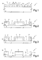
- Figure 1 illustrates a semiconductor wafer 1, e.g. of monocrystalline silicon, comprising a substrate 2.
- a resist mask 3 is initially deposited and shaped.
- the mask 3 has a plurality of rectilinear openings 5, arranged parallel to one another and extending in a direction perpendicular to the plane of the drawing.
- the openings 5 all have a same width W, for example equal to 1 ⁇ m, and are evenly spaced apart.
- the spacing S between adjacent openings 5 is substantially equal to the width W.
- a passivating layer 6 of polymeric material is formed on the wafer 1. More precisely, the passivating layer 6 is conformally deposited and coats the mask 3 and the substrate 2 where this is left exposed, i.e., within the openings 5, with a substantially constant thickness. Also the surfaces perpendicular to the surface 2a of the substrate 2 (vertical) are coated with the passivating layer 6.
- a directional etch is carried out using an aggressive agent, preferably SF 6 .
- an aggressive agent preferably SF 6 .
- the etching rate is favoured as against the directionality.
- FIG. 3 an intermediate step of the directional etch is illustrated.
- the passivating layer 6 is gradually eliminated, but not in a uniform way.
- removal is faster within the openings 5 of the mask 3, where the passivating layer 6 is in direct contact with the silicon, which is thus exposed more rapidly than the mask 3.
- the removal of the passivating layer 6 is much slower on the vertical surfaces than on the horizontal ones (respectively perpendicular and parallel to the surface 2a of the substrate 2). Consequently, the silicon of the substrate 2 starts to be etched through the openings 5 before the mask 3 is completely exposed.
- the passivating layer 6 protects the mask 3 to prevent it from being completely removed before the end of the digging process.
- the substrate 2 is principally dug in a direction perpendicular to the surface 2, and trenches 10 start to form.
- the etching agent has been chosen so as to privilege rapidity over directionality, the trenches 10 tend to expand also in a transverse direction with respect to the principal direction of etching.
- the directional etch terminates after the passivating layer 6 has been completely removed and the trenches 10 have reached a pre-set depth. Furthermore, the mask 3 has been slightly eroded.
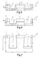
- a new passivating layer 6' is conformally deposited, which coats the mask 3 and the surfaces that delimit the trenches 10, as illustrated in Figure 5. Then ( Figure 6), the wafer 1 is again directionally etched through the openings 5 of the mask 2, until the passivating layer 6' has been completely removed.
- the steps of passivation and of directional etching through the openings 5 are repeated in sequence for a pre-determined number of times (for example eight times, as illustrated in Figure 7).
- the depth of the trenches 10 increases substantially by the same amount at each iteration of the directional etch, and the side surfaces 10a that delimit the trenches 10 assume a corrugated profile.
- the passivation becomes less effective as the depth increases, and hence the side surfaces 10a are less protected during the etching operations.
- spacer portions 10' of the trenches 10 dug up to this moment have a width W' that on average increases (considering the corrugated profile of the side surfaces 10a) as the depth D, i.e., the depth of the distance from the surface 2a of the substrate 2, increases.
- tapered portions 10" of the trenches 10 are formed, which have a width W" decreasing as the depth D increases.
- a polymerizing plasma etch is carried out, in controlled plasma conditions, through the openings 5 of the mask 3.
- the polymerizing etch is preferably an STI (Shallow Trench Isolation) etch, which, however, is performed starting from a trench already partially formed, instead of directly on the surface 2a of the substrate 2.
- STI Shallow Trench Isolation
- the etching speed is much lower than before and, in a transverse direction with respect to the principal direction of etching, the rate of deposition of polymeric material prevails over the rate of removal.
- the side surfaces 10a of the trenches 10 are then coated with a protective layer 11 of increasing thickness, and hence the exposed part of the substrate 2 narrows. Consequently, the width W" of the tapered portion 10" gradually diminishes.
- the composition and conditions of the plasma are selected so that the side surfaces 10a of the tapered portion 10" of the trench 10 have an angle of inclination ⁇ which is controlled and preferably constant with respect to the surface 2a of the substrate 2, irrespective of the depth D ( Figure 9).
- the angle of inclination ⁇ is equal to approximately 85°.
- the height H of the tapered portions 10" is such that the inclination of the side surfaces 10a compensates for the widening of the portions of the overlying trenches 10 with respect to the width of the openings 5 of the mask 3.
- a first digging cycle is thus concluded, which comprises the steps described above: first steps of passivation and of directional etch carried out in sequence a pre-determined number of times to form a spacing portion 10'; and then a polymerizing etching step to form the tapered portions 10" of the trenches 10.
- the polymerizing etch is performed before the sequence of steps of passivation and directional etch.
- each of the trenches 10 comprises three respective tapered portions 10", each of which has a width W" decreasing as the depth D increases with respect to the surface 2a of the substrate 2.
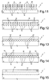
- adjacent trenches 10 define diaphragms 12, arranged so as to form a comb-like structure, as illustrated in Figure 11 (for reasons of simplicity, the side surfaces 10a of the trenches 10 are herein illustrated as if they were vertical).
- an epitaxial layer 15 is grown, which closes the trenches 10 at the top, filling them partially and forming buried cavities 13.
- the epitaxial growth is carried out in a deoxidizing environment, rich in hydrogen molecules, which are trapped within the buried cavities 13.
- a thermal step of annealing is then executed ( Figure 13).
- the wafer 1 is heated at a controlled temperature for a pre-determined period of time (for example, 1150°C for 1 h).
- the semiconductor material forming the diaphragms 12 is subject to migration and tends to redistribute according to a configuration of minimum energy, maintaining in any case the order of the monocrystal.
- the diaphragms tend to thin out and, at the same time, the height of the buried cavities 13 decreases slightly.
- access openings 16 are provided for supplying oxygen to the buried cavities 13 (further access openings, not illustrated, extend in a perpendicular direction, forming a lattice, so that all the buried cavities 13 will be reachable from outside).
- a thermal oxidation is then carried out, where the diaphragms 12 are completely oxidized, and the buried cavities 13 fill up with silicon oxide. Consequently, at the end of the oxidation process, a buried dielectric layer 18 is obtained, as illustrated in Figure 15.
- the buried dielectric layer 18 extends over all the substrate 2, separating it from the epitaxial layer 15.
- the process described is advantageous because it enables deep trenches with a substantially constant width to be obtained rapidly, preventing significant deviations with respect to a desired width.
- the process described can be advantageously used when it is necessary to define thin diaphragms, having a height much greater than the thickness.
- the thickness of the diaphragms can be easily controlled to avoid that the excessive thinning may cause collapse during digging of the trenches or in subsequent process steps (for example, during epitaxial growth).
- the control of the thickness of the diaphragms is particularly important also in view of the subsequent steps of annealing and of thermal oxidation. Thicknesses that are too great or, on the other hand, too small could in fact cause an incomplete oxidation of the diaphragms or lack of uniformity of the buried dielectric layer, which could include residual cavities of significant dimensions.
Landscapes
- Drying Of Semiconductors (AREA)
- Element Separation (AREA)
Abstract
Description
- The present invention relates to a process for process for digging a deep trench in a semiconductor body and semiconductor body so obtained.
- As is known, in different processes of fabrication of semiconductor devices, it is necessary to form deep trenches within semiconductor wafers. In practice, trenches must be opened, which have a depth much greater than at least one transverse dimension. For this purpose, various methods have been developed, which enable removal of semiconductor material in a markedly directional way, as a rule perpendicular to the surface of the semiconductor wafer, whereas the efficiency of etching in a direction transverse with respect to the digging direction is in principle negligible.
- Frequently, however, conflicting requirements must be satisfied. In particular, favouring directionality of an etching step frequently leads to sacrificing speed, and vice versa.
- To overcome the above drawback, a known method envisages alternation of etching steps, which are far from directional but very aggressive, and steps of passivation, which protect the structures surrounding the digging in a direction transverse to the etching direction. In practice, after forming a resist mask that exposes portions of the surface of a semiconductor wafer that are to be etched, a polymeric passivating layer is conformally deposited. The wafer is then immersed in an etching fluid, for example SF6, which, after eliminating the passivating layer, etches the underlying structures. However, the passivating layer is more rapidly removed on the semiconductor material than on the resist and much more rapidly on the surfaces substantially parallel to the surface of the wafer than on the perpendicular surfaces. Consequently, the digging proceeds initially in a direction substantially perpendicular to the surface of the wafer and only to a minimal extent in a transverse direction. When the passivating layer has been almost completely removed, the etching process is interrupted and a new passivating layer is formed. A subsequent etching step will thus resume the process of aggression of the semiconductor material in a direction substantially perpendicular to the surface of the wafer, whereas the walls around the trench that is being formed are protected. By alternating the described etching and passivation steps, it is possible to safeguard the directionality of the etch as a whole and at the same time maintain a satisfactory speed.
- Control of the etch in a direction transverse to the digging direction, however, is less and less precise as the depth increases and may become critical if it is necessary to form a plurality of trenches close to one another, separated by thin diaphragms of semiconductor material, as in the case of some processes of fabrication of SOI (Silicon On Insulator) wafers. In depth, in fact, the deposition of the passivating layer is less effective, and hence the walls of the trenches are less protected. The etch, then, tends to lose directionality, and the trenches widen, whereas the diaphragms thin out towards the base, with the risk of collapsing. The initial thickness of the diaphragms (i.e., towards the surface of the wafer) must be oversized to prevent any failure. Furthermore, in order to favour polymerization and hence formation of the passivating layer, the process must be performed at temperatures that are significantly lower than the ones required for normal etching processes (below room temperature or even at temperatures lower than 0°C), but for this purpose special machinery is required.
- The aim of the present invention is to provide a process for digging a deep trench in a body of semiconductor material and a semiconductor body that are free from the drawbacks described.
- According to the present invention, a process for digging a deep trench in a body of semiconductor material and a semiconductor body are provided, as defined in
Claims - For a better understanding of the invention, an embodiment thereof will now be described purely by way of non-limiting example and with reference to the attached plate of drawings, wherein:
- Figure 1 shows a cross section through a semiconductor wafer, in an initial step of a process according to an embodiment of the present invention;
- Figures 2-9 show an enlarged detail of the wafer illustrated in Figure 1, in successive fabrication steps;
- Figure 9a shows a variant of the process according to the invention; and
- Figures 10-15 show the view of Figures 1-9, in final fabrication steps of the present process.
- Figure 1 illustrates a
semiconductor wafer 1, e.g. of monocrystalline silicon, comprising asubstrate 2. On a (horizontal)surface 2a of thesubstrate 2, aresist mask 3 is initially deposited and shaped. Themask 3 has a plurality ofrectilinear openings 5, arranged parallel to one another and extending in a direction perpendicular to the plane of the drawing. Theopenings 5 all have a same width W, for example equal to 1 µm, and are evenly spaced apart. Preferably, the spacing S betweenadjacent openings 5 is substantially equal to the width W. - As illustrated in the enlargement of Figure 2, a
passivating layer 6 of polymeric material is formed on thewafer 1. More precisely, thepassivating layer 6 is conformally deposited and coats themask 3 and thesubstrate 2 where this is left exposed, i.e., within theopenings 5, with a substantially constant thickness. Also the surfaces perpendicular to thesurface 2a of the substrate 2 (vertical) are coated with thepassivating layer 6. - Subsequently, a directional etch is carried out using an aggressive agent, preferably SF6. In this step, the etching rate is favoured as against the directionality.
- In Figure 3, an intermediate step of the directional etch is illustrated. As may be noted, the
passivating layer 6 is gradually eliminated, but not in a uniform way. In particular, removal is faster within theopenings 5 of themask 3, where thepassivating layer 6 is in direct contact with the silicon, which is thus exposed more rapidly than themask 3. Furthermore, the removal of thepassivating layer 6 is much slower on the vertical surfaces than on the horizontal ones (respectively perpendicular and parallel to thesurface 2a of the substrate 2). Consequently, the silicon of thesubstrate 2 starts to be etched through theopenings 5 before themask 3 is completely exposed. In this step, thepassivating layer 6 protects themask 3 to prevent it from being completely removed before the end of the digging process. - As the directional etch proceeds (Figure 4), the
substrate 2 is principally dug in a direction perpendicular to thesurface 2, and trenches 10 start to form. However, given that the etching agent has been chosen so as to privilege rapidity over directionality, thetrenches 10 tend to expand also in a transverse direction with respect to the principal direction of etching. The directional etch terminates after thepassivating layer 6 has been completely removed and thetrenches 10 have reached a pre-set depth. Furthermore, themask 3 has been slightly eroded. - Subsequently, a new passivating layer 6' is conformally deposited, which coats the
mask 3 and the surfaces that delimit thetrenches 10, as illustrated in Figure 5. Then (Figure 6), thewafer 1 is again directionally etched through theopenings 5 of themask 2, until the passivating layer 6' has been completely removed. - The steps of passivation and of directional etching through the
openings 5 are repeated in sequence for a pre-determined number of times (for example eight times, as illustrated in Figure 7). The depth of thetrenches 10 increases substantially by the same amount at each iteration of the directional etch, and theside surfaces 10a that delimit thetrenches 10 assume a corrugated profile. However, the passivation becomes less effective as the depth increases, and hence theside surfaces 10a are less protected during the etching operations. Consequently, spacer portions 10' of thetrenches 10 dug up to this moment have a width W' that on average increases (considering the corrugated profile of theside surfaces 10a) as the depth D, i.e., the depth of the distance from thesurface 2a of thesubstrate 2, increases. - With reference to Figures 8 and 9, after the sequences of passivation and directional etching have been repeated for the pre-set number of times, tapered
portions 10" of thetrenches 10 are formed, which have a width W" decreasing as the depth D increases. For this purpose, a polymerizing plasma etch is carried out, in controlled plasma conditions, through theopenings 5 of themask 3. The polymerizing etch is preferably an STI (Shallow Trench Isolation) etch, which, however, is performed starting from a trench already partially formed, instead of directly on thesurface 2a of thesubstrate 2. In this step, the process described inEP-A-1 376 683 , filed in the name of the present applicant, can be used. - In this step, the etching speed is much lower than before and, in a transverse direction with respect to the principal direction of etching, the rate of deposition of polymeric material prevails over the rate of removal. As the etching operation proceeds, the
side surfaces 10a of thetrenches 10 are then coated with aprotective layer 11 of increasing thickness, and hence the exposed part of thesubstrate 2 narrows. Consequently, the width W" of thetapered portion 10" gradually diminishes. - During the polymerizing etch, the composition and conditions of the plasma (pressure, temperature, voltage with respect to the
wafer 1, RF power) are selected so that theside surfaces 10a of thetapered portion 10" of thetrench 10 have an angle of inclination α which is controlled and preferably constant with respect to thesurface 2a of thesubstrate 2, irrespective of the depth D (Figure 9). For example, the angle of inclination α is equal to approximately 85°. Furthermore, the height H of thetapered portions 10" is such that the inclination of theside surfaces 10a compensates for the widening of the portions of theoverlying trenches 10 with respect to the width of theopenings 5 of themask 3. - Once the polymerizing etch is terminated, the structure illustrated in Figure 9 is obtained.
- A first digging cycle is thus concluded, which comprises the steps described above: first steps of passivation and of directional etch carried out in sequence a pre-determined number of times to form a spacing portion 10'; and then a polymerizing etching step to form the
tapered portions 10" of thetrenches 10. According to a variant (see Figure 9a), the polymerizing etch is performed before the sequence of steps of passivation and directional etch. This solution provides for the creation of a protective layer already during the first etching steps and is particularly effective when the maintenance of the transverse dimensions right from the start of the digging operation is of a critical nature. - Subsequently (Figure 10), further digging cycles are carried out identical to the first digging cycle described above, until the
trenches 10 have a desired depth. In the example illustrated in Figure 10, three digging cycles have been carried out in all. Consequently, each of thetrenches 10 comprises three respectivetapered portions 10", each of which has a width W" decreasing as the depth D increases with respect to thesurface 2a of thesubstrate 2. - At this point,
adjacent trenches 10 definediaphragms 12, arranged so as to form a comb-like structure, as illustrated in Figure 11 (for reasons of simplicity, the side surfaces 10a of thetrenches 10 are herein illustrated as if they were vertical). After removal of themask 3 and possible residue of polymeric material within the trenches 10 (Figure 12), anepitaxial layer 15 is grown, which closes thetrenches 10 at the top, filling them partially and forming buriedcavities 13. The epitaxial growth is carried out in a deoxidizing environment, rich in hydrogen molecules, which are trapped within the buriedcavities 13. - By exploiting the deoxidizing environment within the buried
cavities 13, a thermal step of annealing is then executed (Figure 13). In practice, thewafer 1 is heated at a controlled temperature for a pre-determined period of time (for example, 1150°C for 1 h). In these conditions, the semiconductor material forming thediaphragms 12 is subject to migration and tends to redistribute according to a configuration of minimum energy, maintaining in any case the order of the monocrystal. In practice, the diaphragms tend to thin out and, at the same time, the height of the buriedcavities 13 decreases slightly. - Next (Figure 14),
access openings 16 are provided for supplying oxygen to the buried cavities 13 (further access openings, not illustrated, extend in a perpendicular direction, forming a lattice, so that all the buriedcavities 13 will be reachable from outside). A thermal oxidation is then carried out, where thediaphragms 12 are completely oxidized, and the buriedcavities 13 fill up with silicon oxide. Consequently, at the end of the oxidation process, a burieddielectric layer 18 is obtained, as illustrated in Figure 15. The burieddielectric layer 18 extends over all thesubstrate 2, separating it from theepitaxial layer 15. - The process described is advantageous because it enables deep trenches with a substantially constant width to be obtained rapidly, preventing significant deviations with respect to a desired width. In particular, the process described can be advantageously used when it is necessary to define thin diaphragms, having a height much greater than the thickness. In this case, in fact, the thickness of the diaphragms can be easily controlled to avoid that the excessive thinning may cause collapse during digging of the trenches or in subsequent process steps (for example, during epitaxial growth). In the case of fabrication of SOI wafers as described, the control of the thickness of the diaphragms is particularly important also in view of the subsequent steps of annealing and of thermal oxidation. Thicknesses that are too great or, on the other hand, too small could in fact cause an incomplete oxidation of the diaphragms or lack of uniformity of the buried dielectric layer, which could include residual cavities of significant dimensions.
- Finally, it is evident that modifications and variations may be made to the process described herein, without departing from the scope of the present invention as defined in the annexed claims. In particular, in each digging cycle, the sequence of steps of passivation and directional etching can be repeated an arbitrary number of times before the polymerizing etch is carried out (or after it has been carried out). Consequently, the length of the sequences of steps of passivation and directional etching may be constant in each digging cycle, but different with respect to what is described above, or else, it can vary from one digging cycle to another.
Claims (13)
- A process for digging a deep trench in a body of semiconductor material, comprising the steps of:- on a surface (2a) of a semiconductor body (2), forming a mask (3) having at least one opening (5);- forming a passivating layer (6, 6') conformally on said mask (3) and on said semiconductor body (2) within said opening (5);- executing a directional etch so as to first remove said passivating layer (6, 6') at least from above said semiconductor body (2) and then etch said semiconductor body (2) through said opening (5);wherein said steps of forming a passivating layer (6, 6') and executing a directional etch are carried out repeatedly in sequence so as to form a trench (10) through said opening (5);
characterized in that it comprises the step of forming a tapered portion (10") of said trench (10), having a transverse dimension (W") decreasing as a distance (D) from said surface (2a) increases. - The process according to Claim 1, wherein a plurality of digging cycles is executed and wherein each digging cycle comprises:- a pre-determined number of said steps of forming a passivating layer (6, 6') and of executing a directional etch, in sequence; and- a step of forming a tapered portion (10").
- The process according to Claim 2, wherein three said digging cycles are carried out.
- The process according to Claim 2 or Claim 3, wherein said pre-determined number is equal to eight.
- The process according to any one of the preceding claims, wherein said step of forming said tapered portion (10") comprises executing a polymerizing etch through said opening (5).
- The process according to Claim 5, wherein said step of executing a polymerizing etch comprises controlling an angle of inclination (α) of side surfaces (10a) of said tapered portion (10") of said trench (10).
- The process according to Claim 6, wherein said angle of inclination (α) is substantially constant and is equal to approximately 85° with respect to said surface (2a) of said semiconductor body (2).
- A manufacturing process of a SOI wafer, comprising the step of digging, in a substrate (2) of semiconductor material, a plurality of rectilinear and parallel trenches (10), separated from one another by diaphragms (12) of semiconductor material, characterized in that said step of digging is carried out according to any one of the preceding claims.
- The process according to Claim 8, comprising the step of growing an epitaxial layer (15) starting from said diaphragms (12), so as to close said trenches (10) and form buried cavities (13).
- The process according to Claim 9, comprising a step of annealing of said wafer (1), for reconfiguring said diaphragms (12) and said buried cavities (13).
- The process according to Claim 10, comprising the step of oxidizing thermally said diaphragms (12).
- A semiconductor body, having a surface (2a) and comprising at least one trench (10) open at said surface (2a), wherein said trench (10) includes at least one spacing portion (10'), having a width (W') that on average increases as a distance (D) from said surface (2a) increases;
characterized in that said trench (10) comprises at least one tapered portion (10"), which has a width (W") that decreases as a distance (D) from said surface (2a) increases. - The semiconductor body according to Claim 12, comprising a plurality of said tapered portions (10"), separated by a respective spacing portions (10').
Priority Applications (2)
| Application Number | Priority Date | Filing Date | Title |
|---|---|---|---|
| EP05425930A EP1804281B1 (en) | 2005-12-28 | 2005-12-28 | Process for digging a deep trench in a semiconductor body and semiconductor body so obtained |
| US11/648,838 US7544620B2 (en) | 2005-12-28 | 2006-12-28 | Process for digging a deep trench in a semiconductor body and semiconductor body so obtained |
Applications Claiming Priority (1)
| Application Number | Priority Date | Filing Date | Title |
|---|---|---|---|
| EP05425930A EP1804281B1 (en) | 2005-12-28 | 2005-12-28 | Process for digging a deep trench in a semiconductor body and semiconductor body so obtained |
Publications (2)
| Publication Number | Publication Date |
|---|---|
| EP1804281A1 true EP1804281A1 (en) | 2007-07-04 |
| EP1804281B1 EP1804281B1 (en) | 2011-12-14 |
Family
ID=36215520
Family Applications (1)
| Application Number | Title | Priority Date | Filing Date |
|---|---|---|---|
| EP05425930A Expired - Lifetime EP1804281B1 (en) | 2005-12-28 | 2005-12-28 | Process for digging a deep trench in a semiconductor body and semiconductor body so obtained |
Country Status (2)
| Country | Link |
|---|---|
| US (1) | US7544620B2 (en) |
| EP (1) | EP1804281B1 (en) |
Families Citing this family (16)
| Publication number | Priority date | Publication date | Assignee | Title |
|---|---|---|---|---|
| JP6160044B2 (en) * | 2012-08-30 | 2017-07-12 | 富士電機株式会社 | Manufacturing method of semiconductor device |
| US9257337B2 (en) | 2013-04-17 | 2016-02-09 | Industrial Technology Research Institute | Semiconductor structure and manufacturing method thereof |
| TWI492345B (en) | 2013-04-17 | 2015-07-11 | 財團法人工業技術研究院 | Semiconductor structure and manufacturing method thereof |
| US9496337B2 (en) * | 2013-12-19 | 2016-11-15 | Infineon Technologies Austria Ag | Method for producing a semiconductor device having a beveled edge termination |
| US9935126B2 (en) * | 2014-09-08 | 2018-04-03 | Infineon Technologies Ag | Method of forming a semiconductor substrate with buried cavities and dielectric support structures |
| US9536999B2 (en) | 2014-09-08 | 2017-01-03 | Infineon Technologies Ag | Semiconductor device with control structure including buried portions and method of manufacturing |
| CN105719965A (en) * | 2014-12-04 | 2016-06-29 | 北京北方微电子基地设备工艺研究中心有限责任公司 | Method and device for etching silicon dioxide substrate |
| DE102016119799B4 (en) * | 2016-10-18 | 2020-08-06 | Infineon Technologies Ag | INTEGRATED CIRCUIT CONTAINING A CURVED CAVE AND PRODUCTION METHOD |
| CN112018089B (en) * | 2019-05-31 | 2023-05-26 | 芯恩(青岛)集成电路有限公司 | Semiconductor capacitor and method for manufacturing the same |
| US11121085B2 (en) * | 2019-09-24 | 2021-09-14 | Micron Technology, Inc. | Trench walls, conductive structures having different widths and methods of making same |
| US20210118734A1 (en) * | 2019-10-22 | 2021-04-22 | Semiconductor Components Industries, Llc | Plasma-singulated, contaminant-reduced semiconductor die |
| DE102021200431A1 (en) * | 2021-01-19 | 2022-07-21 | Robert Bosch Gesellschaft mit beschränkter Haftung | Method for forming a trench in a first semiconductor layer of a multilayer system |
| JP7853127B2 (en) * | 2022-03-16 | 2026-04-28 | 株式会社ディスコ | Chip manufacturing method |
| US20240258112A1 (en) * | 2023-01-30 | 2024-08-01 | Texas Instruments Incorporated | Multi-loop time varying bosch process for 2-dimensional small cd high aspect ratio deep silicon trench etching |
| CN117238840B (en) * | 2023-11-14 | 2024-02-27 | 合肥晶合集成电路股份有限公司 | Backside illuminated image sensor, preparation method thereof and preparation method of deep trench isolation structure |
| CN119626901B (en) * | 2024-09-18 | 2025-12-30 | 浙江创芯集成电路有限公司 | Methods for forming semiconductor structures |
Citations (4)
| Publication number | Priority date | Publication date | Assignee | Title |
|---|---|---|---|---|
| EP0822582A2 (en) | 1996-08-01 | 1998-02-04 | Surface Technology Systems Limited | Method of surface treatment of semiconductor substrates |
| EP0964456A2 (en) | 1998-06-09 | 1999-12-15 | Siemens Aktiengesellschaft | Deep trench capacitor |
| US6187685B1 (en) * | 1997-08-01 | 2001-02-13 | Surface Technology Systems Limited | Method and apparatus for etching a substrate |
| US6284148B1 (en) * | 1997-08-21 | 2001-09-04 | Robert Bosch Gmbh | Method for anisotropic etching of silicon |
Family Cites Families (6)
| Publication number | Priority date | Publication date | Assignee | Title |
|---|---|---|---|---|
| GB9616225D0 (en) * | 1996-08-01 | 1996-09-11 | Surface Tech Sys Ltd | Method of surface treatment of semiconductor substrates |
| US7294536B2 (en) * | 2000-07-25 | 2007-11-13 | Stmicroelectronics S.R.L. | Process for manufacturing an SOI wafer by annealing and oxidation of buried channels |
| WO2004028952A2 (en) * | 2002-06-26 | 2004-04-08 | Cornell Research Foundation, Inc. | Small scale wires with microelectromechanical devices |
| EP1376683B1 (en) | 2002-06-28 | 2007-03-07 | STMicroelectronics S.r.l. | Process for forming trenches with oblique profile and rounded top corners |
| US7056830B2 (en) * | 2003-09-03 | 2006-06-06 | Applied Materials, Inc. | Method for plasma etching a dielectric layer |
| DE102004043356A1 (en) * | 2004-09-08 | 2006-03-09 | Robert Bosch Gmbh | Sensor element with trenched cavern |
-
2005
- 2005-12-28 EP EP05425930A patent/EP1804281B1/en not_active Expired - Lifetime
-
2006
- 2006-12-28 US US11/648,838 patent/US7544620B2/en active Active
Patent Citations (4)
| Publication number | Priority date | Publication date | Assignee | Title |
|---|---|---|---|---|
| EP0822582A2 (en) | 1996-08-01 | 1998-02-04 | Surface Technology Systems Limited | Method of surface treatment of semiconductor substrates |
| US6187685B1 (en) * | 1997-08-01 | 2001-02-13 | Surface Technology Systems Limited | Method and apparatus for etching a substrate |
| US6284148B1 (en) * | 1997-08-21 | 2001-09-04 | Robert Bosch Gmbh | Method for anisotropic etching of silicon |
| EP0964456A2 (en) | 1998-06-09 | 1999-12-15 | Siemens Aktiengesellschaft | Deep trench capacitor |
Also Published As
| Publication number | Publication date |
|---|---|
| US7544620B2 (en) | 2009-06-09 |
| US20070190743A1 (en) | 2007-08-16 |
| EP1804281B1 (en) | 2011-12-14 |
Similar Documents
| Publication | Publication Date | Title |
|---|---|---|
| EP1804281B1 (en) | Process for digging a deep trench in a semiconductor body and semiconductor body so obtained | |
| KR100369324B1 (en) | Method for fabricating planar type micro cavity | |
| CN102239540B (en) | Methods of fabricating substrates | |
| US20020166838A1 (en) | Sloped trench etching process | |
| CN213124449U (en) | Electronic Power Devices | |
| JP2006237643A (en) | Process for forming embedded cavity in semiconductor material wafer, and the embedded cavity | |
| JP2008306003A (en) | Manufacturing method of semiconductor device | |
| JP4686544B2 (en) | Method for etching a layer on a substrate | |
| CN102239541A (en) | Methods of fabricating substrates | |
| KR20170034984A (en) | Dummy wafer, a method of forming thin film and a method of a semiconductor device | |
| JP5413331B2 (en) | Manufacturing method of semiconductor device | |
| JP2009182059A (en) | Dry etching method | |
| US9147579B2 (en) | Method of manufacturing a semiconductor device and a semiconductor device | |
| KR102711638B1 (en) | Control of silicon nitride etching and silica deposition in 3D NAND structures | |
| EP1376683B1 (en) | Process for forming trenches with oblique profile and rounded top corners | |
| CN100474563C (en) | Process for dividing integrated devices in thin semiconductor chips | |
| US5437739A (en) | Etch control seal for dissolved wafer micromachining process | |
| JP7757541B2 (en) | Power device structure and manufacturing method thereof | |
| CN102693911A (en) | Dry etching method | |
| CN115274552B (en) | Preparation method of semiconductor surface slot and preparation method of IGBT device surface slot | |
| US8030157B1 (en) | Liner protection in deep trench etching | |
| JP5012856B2 (en) | Manufacturing method of semiconductor device | |
| CN111115561B (en) | Preparation method of micro-nano through hole and structure with micro-nano through hole | |
| KR100923761B1 (en) | How to Form Shallow Trench Isolation | |
| KR100275501B1 (en) | How to form a trench |
Legal Events
| Date | Code | Title | Description |
|---|---|---|---|
| PUAI | Public reference made under article 153(3) epc to a published international application that has entered the european phase |
Free format text: ORIGINAL CODE: 0009012 |
|
| AK | Designated contracting states |
Kind code of ref document: A1 Designated state(s): AT BE BG CH CY CZ DE DK EE ES FI FR GB GR HU IE IS IT LI LT LU LV MC NL PL PT RO SE SI SK TR |
|
| AX | Request for extension of the european patent |
Extension state: AL BA HR MK YU |
|
| 17P | Request for examination filed |
Effective date: 20080102 |
|
| 17Q | First examination report despatched |
Effective date: 20080205 |
|
| AKX | Designation fees paid |
Designated state(s): DE FR GB IT |
|
| RAP1 | Party data changed (applicant data changed or rights of an application transferred) |
Owner name: STMICROELECTRONICS SRL |
|
| GRAP | Despatch of communication of intention to grant a patent |
Free format text: ORIGINAL CODE: EPIDOSNIGR1 |
|
| GRAS | Grant fee paid |
Free format text: ORIGINAL CODE: EPIDOSNIGR3 |
|
| GRAA | (expected) grant |
Free format text: ORIGINAL CODE: 0009210 |
|
| AK | Designated contracting states |
Kind code of ref document: B1 Designated state(s): DE FR GB IT |
|
| REG | Reference to a national code |
Ref country code: GB Ref legal event code: FG4D |
|
| REG | Reference to a national code |
Ref country code: DE Ref legal event code: R096 Ref document number: 602005031636 Country of ref document: DE Effective date: 20120209 |
|
| RAP2 | Party data changed (patent owner data changed or rights of a patent transferred) |
Owner name: STMICROELECTRONICS SRL |
|
| PLBE | No opposition filed within time limit |
Free format text: ORIGINAL CODE: 0009261 |
|
| STAA | Information on the status of an ep patent application or granted ep patent |
Free format text: STATUS: NO OPPOSITION FILED WITHIN TIME LIMIT |
|
| 26N | No opposition filed |
Effective date: 20120917 |
|
| REG | Reference to a national code |
Ref country code: FR Ref legal event code: ST Effective date: 20121019 |
|
| GBPC | Gb: european patent ceased through non-payment of renewal fee |
Effective date: 20120314 |
|
| PG25 | Lapsed in a contracting state [announced via postgrant information from national office to epo] |
Ref country code: IT Free format text: LAPSE BECAUSE OF FAILURE TO SUBMIT A TRANSLATION OF THE DESCRIPTION OR TO PAY THE FEE WITHIN THE PRESCRIBED TIME-LIMIT Effective date: 20111214 |
|
| REG | Reference to a national code |
Ref country code: DE Ref legal event code: R097 Ref document number: 602005031636 Country of ref document: DE Effective date: 20120917 |
|
| PG25 | Lapsed in a contracting state [announced via postgrant information from national office to epo] |
Ref country code: FR Free format text: LAPSE BECAUSE OF NON-PAYMENT OF DUE FEES Effective date: 20120214 Ref country code: GB Free format text: LAPSE BECAUSE OF NON-PAYMENT OF DUE FEES Effective date: 20120314 |
|
| REG | Reference to a national code |
Ref country code: DE Ref legal event code: R082 Ref document number: 602005031636 Country of ref document: DE Representative=s name: BOEHMERT & BOEHMERT, DE |
|
| REG | Reference to a national code |
Ref country code: DE Ref legal event code: R081 Ref document number: 602005031636 Country of ref document: DE Owner name: MICRON TECHNOLOGY, INC., BOISE, US Free format text: FORMER OWNER: STMICROELECTRONICS S.R.L., AGRATE BRIANZA, IT Effective date: 20111216 Ref country code: DE Ref legal event code: R081 Ref document number: 602005031636 Country of ref document: DE Owner name: MICRON TECHNOLOGY, INC., BOISE, US Free format text: FORMER OWNER: STMICROELECTRONICS SRL, AGRATE BRIANZA, IT Effective date: 20130312 Ref country code: DE Ref legal event code: R082 Ref document number: 602005031636 Country of ref document: DE Representative=s name: BOEHMERT & BOEHMERT ANWALTSPARTNERSCHAFT MBB -, DE Effective date: 20130312 Ref country code: DE Ref legal event code: R081 Ref document number: 602005031636 Country of ref document: DE Owner name: MICRON TECHNOLOGY, INC., BOISE, US Free format text: FORMER OWNER: STMICROELECTRONICS S.R.L., AGRATE BRIANZA, MAILAND/MILANO, IT Effective date: 20111216 Ref country code: DE Ref legal event code: R081 Ref document number: 602005031636 Country of ref document: DE Owner name: MICRON TECHNOLOGY, INC., US Free format text: FORMER OWNER: STMICROELECTRONICS SRL, AGRATE BRIANZA, IT Effective date: 20130312 Ref country code: DE Ref legal event code: R082 Ref document number: 602005031636 Country of ref document: DE Representative=s name: BOEHMERT & BOEHMERT, DE Effective date: 20130312 Ref country code: DE Ref legal event code: R081 Ref document number: 602005031636 Country of ref document: DE Owner name: MICRON TECHNOLOGY, INC., US Free format text: FORMER OWNER: STMICROELECTRONICS S.R.L., AGRATE BRIANZA, IT Effective date: 20111216 |
|
| PGFP | Annual fee paid to national office [announced via postgrant information from national office to epo] |
Ref country code: DE Payment date: 20241227 Year of fee payment: 20 |
|
| REG | Reference to a national code |
Ref country code: DE Ref legal event code: R079 Ref document number: 602005031636 Country of ref document: DE Free format text: PREVIOUS MAIN CLASS: H01L0021306500 Ipc: H10P0050240000 |
|
| REG | Reference to a national code |
Ref country code: DE Ref legal event code: R071 Ref document number: 602005031636 Country of ref document: DE |