EP1801923A1 - Connector device - Google Patents
Connector device Download PDFInfo
- Publication number
- EP1801923A1 EP1801923A1 EP05301086A EP05301086A EP1801923A1 EP 1801923 A1 EP1801923 A1 EP 1801923A1 EP 05301086 A EP05301086 A EP 05301086A EP 05301086 A EP05301086 A EP 05301086A EP 1801923 A1 EP1801923 A1 EP 1801923A1
- Authority
- EP
- European Patent Office
- Prior art keywords
- connection
- connector device
- members
- connection members
- assembly
- Prior art date
- Legal status (The legal status is an assumption and is not a legal conclusion. Google has not performed a legal analysis and makes no representation as to the accuracy of the status listed.)
- Granted
Links
Images


Classifications
-
- H—ELECTRICITY
- H01—ELECTRIC ELEMENTS
- H01R—ELECTRICALLY-CONDUCTIVE CONNECTIONS; STRUCTURAL ASSOCIATIONS OF A PLURALITY OF MUTUALLY-INSULATED ELECTRICAL CONNECTING ELEMENTS; COUPLING DEVICES; CURRENT COLLECTORS
- H01R13/00—Details of coupling devices of the kinds covered by groups H01R12/70 or H01R24/00 - H01R33/00
- H01R13/02—Contact members
- H01R13/22—Contacts for co-operating by abutting
- H01R13/24—Contacts for co-operating by abutting resilient; resiliently-mounted
-
- H—ELECTRICITY
- H01—ELECTRIC ELEMENTS
- H01R—ELECTRICALLY-CONDUCTIVE CONNECTIONS; STRUCTURAL ASSOCIATIONS OF A PLURALITY OF MUTUALLY-INSULATED ELECTRICAL CONNECTING ELEMENTS; COUPLING DEVICES; CURRENT COLLECTORS
- H01R12/00—Structural associations of a plurality of mutually-insulated electrical connecting elements, specially adapted for printed circuits, e.g. printed circuit boards [PCB], flat or ribbon cables, or like generally planar structures, e.g. terminal strips, terminal blocks; Coupling devices specially adapted for printed circuits, flat or ribbon cables, or like generally planar structures; Terminals specially adapted for contact with, or insertion into, printed circuits, flat or ribbon cables, or like generally planar structures
- H01R12/70—Coupling devices
- H01R12/71—Coupling devices for rigid printing circuits or like structures
- H01R12/712—Coupling devices for rigid printing circuits or like structures co-operating with the surface of the printed circuit or with a coupling device exclusively provided on the surface of the printed circuit
-
- H—ELECTRICITY
- H01—ELECTRIC ELEMENTS
- H01R—ELECTRICALLY-CONDUCTIVE CONNECTIONS; STRUCTURAL ASSOCIATIONS OF A PLURALITY OF MUTUALLY-INSULATED ELECTRICAL CONNECTING ELEMENTS; COUPLING DEVICES; CURRENT COLLECTORS
- H01R12/00—Structural associations of a plurality of mutually-insulated electrical connecting elements, specially adapted for printed circuits, e.g. printed circuit boards [PCB], flat or ribbon cables, or like generally planar structures, e.g. terminal strips, terminal blocks; Coupling devices specially adapted for printed circuits, flat or ribbon cables, or like generally planar structures; Terminals specially adapted for contact with, or insertion into, printed circuits, flat or ribbon cables, or like generally planar structures
- H01R12/70—Coupling devices
- H01R12/71—Coupling devices for rigid printing circuits or like structures
- H01R12/72—Coupling devices for rigid printing circuits or like structures coupling with the edge of the rigid printed circuits or like structures
- H01R12/721—Coupling devices for rigid printing circuits or like structures coupling with the edge of the rigid printed circuits or like structures cooperating directly with the edge of the rigid printed circuits
-
- H—ELECTRICITY
- H01—ELECTRIC ELEMENTS
- H01R—ELECTRICALLY-CONDUCTIVE CONNECTIONS; STRUCTURAL ASSOCIATIONS OF A PLURALITY OF MUTUALLY-INSULATED ELECTRICAL CONNECTING ELEMENTS; COUPLING DEVICES; CURRENT COLLECTORS
- H01R12/00—Structural associations of a plurality of mutually-insulated electrical connecting elements, specially adapted for printed circuits, e.g. printed circuit boards [PCB], flat or ribbon cables, or like generally planar structures, e.g. terminal strips, terminal blocks; Coupling devices specially adapted for printed circuits, flat or ribbon cables, or like generally planar structures; Terminals specially adapted for contact with, or insertion into, printed circuits, flat or ribbon cables, or like generally planar structures
- H01R12/70—Coupling devices
- H01R12/71—Coupling devices for rigid printing circuits or like structures
- H01R12/75—Coupling devices for rigid printing circuits or like structures connecting to cables except for flat or ribbon cables
Definitions
- the present invention relates to a connector device capable of providing with an electronic card.
- the connector device of the invention presents an autonomous structure whereby actions related to the assembly of cables, installation on supporting bodies and connecting to an electronic card are performed without a need for the connector device to be fixed in place.
- PCB printed circuit board
- a typical structure of a connector for connecting a cable to a PCB usually consists of two parts, one being the so-called aerial part which is fixed to an end of the cable and the other being the so-called fixed part which is fixed onto the PCB.
- the aerial part and the fixed part are structured in such a manner that one is adapted to be engaged with the other, for example by having pins and sockets respectively in conformity with each other, so that the pins may be conveniently introduced in the sockets to ensure a good connection.
- the pins and the sockets are positioned in respective housings which are also engageable with each other when the connection is being performed.
- connectors are a type which provides connection from a PCB to another PCB, such as the so-called PCl connectors generally used in computers.
- a first PCB is provided with connecting pads at one side thereof. The pads are then inserted inside a single connector of a second PCB (the connector may be installed directly on the second PCB or located on a fixed wall of the equipment and connected to the second PCB by means of cables).
- a problem associated with the use of a single connector, as described in relation to the second known example of connectors, is that it is required that the first PCB is inserted into a connector which is fixed in place on the second PCB, or on a wall of the equipment such as a back-plane of a shelf.
- This type of arrangement is limited to only one connection and prevents the card from being simultaneously connected to another connector in a perpendicular plane in the shelf of the equipment because the card can only be inserted in one direction which is the one towards the connector in the second PCB or on the wall of the shelf.
- a connector having two connection members with conductor terminals installed on said members being capable of entering into connection with electronic pads of an electronic card.
- the two members are disposed face to face with respect to each other and are engaged with a moving mechanism which is capable of moving the two members from a first open position in which the two members are at a distance away from each other to provide an empty space there-between for entry of an electronic card, to a second closed position in which the two members are moved towards each other such that when the electronic card is inserted between the two members, its electronic pads enter in contact with the conductor terminals of the connector.
- This structure is particularly useful for connections where the card is entered in contact with various connectors installed in different walls of the shelf.
- a conventional connector with non-movable members
- a connector having movable members as described above, may be installed on a lateral wall of the shelf in order to enter in connection with a lateral edge of the card.
- the card In the open position, the card is inserted in the conventional connector installed in the back-plane and by such insertion, one of its edges slides at the same time in-between the open space provided between the two connection members of the connector with moveable members such that the corresponding edge finally rests in a position in-between said two members.
- the two members are moved, by the moving mechanism, to the closed position, thereby establishing contact between the electronic pads of the card and the conductor terminals of the connector.
- connection points of the connector may be damaged and thus may require repair, for example in order to perform soldering on the terminals.
- This repair task in case of connectors which are fixed in place, may not be possible or at least easy, unless the whole connector is removed from the place it is fixed to. Removal of the connector in such cases, especially when the connector is itself soldered on the wall of the shelf - which is frequently the case - requires extra work.
- the fact that the connector is fixed to the wall of the shelf makes the connector usable only in that position.
- the connector is disconnected from one card and connected to another one, it is the card itself needs to be changed as the connector is fixed in place.
- This change in the case where the other connections of the card (with other connectors on other edges) should not be changed, makes the whole assembly unusable.
- the connector device of the invention is not permanently fixed to any part of the shelf, but is connected to a respective end of a cable (the cable may have a plurality of wires).
- the connector device of the invention allows an easy connection to a metallic pad area at selected edges of an electronic card such as a PCB by opening and closing movements of respective connection.
- the selected edges may be all the four edges of the electronic card or some of the edges thereof, in which case the edges are preferably in perpendicular direction with respect to other edges used for conventional type of connections.
- the other edges may have conventional connectors or may have metallic pads for connection to another PCB or to a back-plane of a shelf in a conventional manner, as described further above.
- the connector device of the invention is suitable for, but not limited to, use in horizontal-cabling plane, i.e. connection is done at a top or bottom side of a front access shelf in which electronic cards are inserted vertically.
- the connector device of the invention may be suitable for use in vertical-cabling i.e. connection is done at a lateral side of a front access shelf in which electronic cards are inserted horizontally.
- one object of the present invention is that of providing a connector device for providing electrical connection between a cable and an electronic card adapted for being installed in a shelf, the connector device comprising two connection members, at least one of said connection members having connection points arranged at selected positions on a respective surface thereof, the two connection members being assembled together by means of an assembly element, the assembly of the two connection members being adapted to have an open position suitable for allowing entry of an electronic card between the two connection members and a closed position suitable for allowing electrical contact between the connection points of the connector device and respective connection pads of the electronic card, characterized in that said open position and said closed position are obtained independently of the position of the connector device with respect to the shelf, and in that the connector device is capable of being moved from one position with respect to the shelf to another position while having the cable connected thereon.
- a connector device 1 having two connector members 11 and 12.
- Each of the two connection members 11, 12 have a plurality of connection points 13, made of electrically conductor material, such as for example copper, installed on selected areas on the surface of the connection members 11, 12 in such a manner that after engagement with an electronic card the connection points enter in contact with connection pads of the electronic card (as will described below), thus providing electrical connectivity there-between.
- the two connection members are joined together by means of an assembly element 15 which will be described further below.
- connection members 11 and 12 are shown to have connection points 13, it is to be understood that the connector device 1 of the invention may also be made with connection points 13 installed only on one of the connection members 11, 12, the other member being without connection points.
- connection points 13 are further connected to the end of a cable 14 in any known manner.
- the cable 14 may have a plurality of conductive wires.
- the connector device of the invention may have the conductive wires already connected thereon before it is installed on an electronic card or fixed on a wall of a shelf.
- Figure 2 shows an electronic card 2, which in this example may be a PCB, having a base plate 21 upon which electronic components and other elements are installed.
- connection pads 22 are installed on a surface of the PCB, or on both front and rear surfaces thereof.
- connection pads 2 may be installed at selected edges of the PCB and other conventional connection elements such as connectors or pads may be installed at other edges of the PCB as represented in figure 2 by reference numeral 25.
- the conventional connection elements 25 may be used for connection in known manners for example to a back-plane of a shelf.
- connection pads 22 may be installed on the upper and lower sides of the PCB.
- connection pads 22 may be installed on the rear surface 24 of the PCB.
- Connection pads 22 on both surfaces 23 and 24 of the PCB are shown in figures 3 and 4.
- the connection pads 22 may be made of any conductive material such as for example copper.
- connection members 11 and 12 are preferably assembled together in such a way that the corresponding sides of the connection members 11 and 12 where connection points 13 are installed may face each other.
- the assembly of the two connection members 11, 12 is made by means of an assembly element 15 such that the assembly element permits one, or the two connection members, to be rotated around the axis of the assembly element 15 with respect to each other or with respect to the assembly element 15.
- the assembly element 15 is in fact installed on the connection members and not on any external supporting piece such as for example the wall of a shelf, which is the case for some known connector devices with moveable connection elements.
- the fact that the assembly element 15 is installed on the connection member has the advantage that in this manner the connector device is made autonomous in the sense that it is capable of being used without a need to be first fixed in place.
- the connector device of the invention is capable of being already connected to the cable 14, for example in manufacturing stage or at any other moment before being installed on the wall of a shelf.
- the connector device is made autonomous is that it may be easily removed from the position of connection on an electronic card in order to be left at a convenient storage place within the shelf until a time when further use is required and thus it is put back in connection with an electronic card, or simply it may be removed from one electronic card and connected on another electronic card inside the shelf.
- the assembly element 15 is assumed to be made by means of a hinge installed at a respective end of each of the two connection members 11,12 such that the two connection members 11 and 12 may rotate around the hinge 15 for opening and closing of the assembly of the connection members 11 and 12 in order to allow insertion or extraction of an electronic card 2 to or from the assembly.
- the assembly of the two connection members 11 and 12 is shown in open position while they are maintained together by means of the hinge 15, and an electronic card 2 is shown to be inserted inside the assembly.
- Figure 4 shows a situation where the two connection members 11, 12 are in closed position and the electronic card 2 is placed inside the assembly.
- the assembly element 15 may be such that each of the connection members 11, 12 may rotate freely around it; or alternatively, provision may be made such that only one of the two connection members 11, 12 is rotateable, the other being fixed with respect to the assembly element 15, in which case one can assume that one connection member rotates with respect to the other - fixed - member.
- the assembly of the two connection members 11 and 12 is equipped with a locking means 16.
- the locking means 16 In figure 3, the locking means 16 is shown in open (unlocked) position while in figure 4, the locking means is shown in locked position.
- the locking means 16 may be of any known type.
- connection points 13 of the connector device 1 enter in physical contact with the connection pads 22 of the electronic card 2 thus ensuring electrical connectivity there-between.
- the assembly may then be locked by means of the locking means 16.
- additional fixing means may be employed (not shown) by means of any known fixing structure such as clips, screws, adhesive material or the like in order to ensure a stronger hold between the connector device 1 and the electronic card 2.
- connection points 13 and that of the connection pads 22 are determined in conformity to each other such that by simple closing action exercised on the connection member 11 and 12, precise connection is achieved between respective connection points 13 and connection pads 22. This conformity in positioning is achieved by adequate layout design of each unit.
- the electronic card 2 may have connection pads 22 installed only on one surface, front 23 or rear 24 thereof.
- the connector device 1 may have connection points 13 installed only on the connection member 11 or 12 which corresponds to the surface of the electronic card on which the electronic pads 22 are installed.
- connection device of the present invention provides the possibility of easily accessing to the connection points 13 in case of need, for example for soldering or cleaning the connection points 13.
- Another advantage of the connection device of the present invention is that in case the connector need to be removed from one card and connected to another, or kept unconnected, this can be done by simply opening the connector device and removing it from the place it was connected without any change in the position of the electronic card.
- FIGs 5a and 5b show schematic representations in front and side view of an alternative embodiment of the connector device of the present invention in which like elements have been given like reference numerals.
- the connector device 1 of figures 5a and 5b has two connection members 11 and 12 and connections points 13 installed on respective surfaces of the connection members 11 and 12.
- Cable 14, which as shown in the figure may be comprised of a plurality of wires is connected to the connection members 11, 12 (however in practice it is possible to have the cable connected to only one of the connection members).
- connection members 11 and 12 are assembled together by means of an assembly element.
- the assembly element is in fact comprised of two assembly members 15a and 15 b placed at respective sides of the connection members 11, 12 in such a way that the connection members 11 and 12 are capable to move side-ways within a space provided between the assembly members 15a and 15b as shown by arrows next to the connection members 11 and 12.
- a third assembly member 15c is also shown in figures 5a and 5b. This third assembly member 15c is capable of moving upward and downward as shown by an arrow.
- the shape of the third assembly element is designed such that when it moves in downward direction, a head portion thereof enters into a space in-between the two connection members 11 and 12 and pushes the latter members side-ways away from each other due to a force exerted on both these members as a result of its downward movement.
- connection members 11, 12 When the two connection members 11, 12 are moved away from each other, sufficient space is provided between the two in order to allow the electronic card 2 enter in-between the connection members 11, 12. Here gain the electronic card 2 is entered in-between the two connection members in such a way that the connection pads 22 of the electronic card are in a position which is in conformity with the connection points 13.
- the third assembly member 15c is made to move outward (upward in figures 5a and 5b) from its position in-between the two connection members 11, 12.
- the two connection members 11, 12 are made to move towards each other.
- the connection points 13 of the connection members 11, 12 enter into contact with the connection pads 22 of the electronic card 2.
- the movement of the two connection members 11, 12 within the space provided in the assembly members 15a and 15b may be governed by any known means.
- the movement may be governed by respective resilient mechanisms such as for example springs (not shown) located between each connection member 11, 12 and the respective assembly members 15a, 15b.
- the movement of the third assembly member 15c may be performed by any known means.
- the assembly member 15c may be made to move up and down in a guiding structure such a sliding rail.
- the assembly element may be made to rotate around a fixed axis located at one side of the connector device.
- locking means may be provided by any known means in order to maintain the whole structure secure as long as the connector device in maintained in contact with the electronic card.
- the connector device of the present invention in any of its embodiments, is capable of being fixed, on a supporting surface, such as for example the wall of a shelf.
- a supporting surface such as for example the wall of a shelf.
- an advantage of the connector device of the invention is that cables may be installed thereupon before it being fixed on a supporting surface. Once the cable is connected, the connector may be fixed, permanently or provisionally, on a supporting surface and it may be connected to an electronic card at any desired time.
- the fixing may be made by any known means such as for example screws and knots.
- connection members may be moved away and toward each other are included within the scope of the present invention.
Landscapes
- Coupling Device And Connection With Printed Circuit (AREA)
- Details Of Connecting Devices For Male And Female Coupling (AREA)
- Connector Housings Or Holding Contact Members (AREA)
- Paper (AREA)
Abstract
Description
- The present invention relates to a connector device capable of providing with an electronic card. In particular the connector device of the invention presents an autonomous structure whereby actions related to the assembly of cables, installation on supporting bodies and connecting to an electronic card are performed without a need for the connector device to be fixed in place.
- Connectors in many varieties of forms and structures are widely used in electronic equipment. One example of use of such connectors in conjunction with electronic cards, such as for example a printed circuit board (hereinafter referred to as PCB).
- A typical structure of a connector for connecting a cable to a PCB usually consists of two parts, one being the so-called aerial part which is fixed to an end of the cable and the other being the so-called fixed part which is fixed onto the PCB. The aerial part and the fixed part are structured in such a manner that one is adapted to be engaged with the other, for example by having pins and sockets respectively in conformity with each other, so that the pins may be conveniently introduced in the sockets to ensure a good connection. The pins and the sockets are positioned in respective housings which are also engageable with each other when the connection is being performed.
- Another example of known connectors is a type which provides connection from a PCB to another PCB, such as the so-called PCl connectors generally used in computers. In this case a first PCB is provided with connecting pads at one side thereof. The pads are then inserted inside a single connector of a second PCB (the connector may be installed directly on the second PCB or located on a fixed wall of the equipment and connected to the second PCB by means of cables).
- One problem associated with using two engaging parts, as described with respect to the first known example of connectors, is that in practice these connectors require a sophisticated assembly.
- On the other hand, a problem associated with the use of a single connector, as described in relation to the second known example of connectors, is that it is required that the first PCB is inserted into a connector which is fixed in place on the second PCB, or on a wall of the equipment such as a back-plane of a shelf. This type of arrangement is limited to only one connection and prevents the card from being simultaneously connected to another connector in a perpendicular plane in the shelf of the equipment because the card can only be inserted in one direction which is the one towards the connector in the second PCB or on the wall of the shelf.
- In order to be able to connect a card simultaneously to various connectors disposed in a various perpendicular planes in the shelf of the equipment, some solutions have been proposed. One of such solutions is that of using a connector having two connection members with conductor terminals installed on said members being capable of entering into connection with electronic pads of an electronic card. The two members are disposed face to face with respect to each other and are engaged with a moving mechanism which is capable of moving the two members from a first open position in which the two members are at a distance away from each other to provide an empty space there-between for entry of an electronic card, to a second closed position in which the two members are moved towards each other such that when the electronic card is inserted between the two members, its electronic pads enter in contact with the conductor terminals of the connector. This structure is particularly useful for connections where the card is entered in contact with various connectors installed in different walls of the shelf. For example, if a conventional connector (with non-movable members) is fixed to the wall of the back-plane of the shelf, a connector having movable members, as described above, may be installed on a lateral wall of the shelf in order to enter in connection with a lateral edge of the card. In the open position, the card is inserted in the conventional connector installed in the back-plane and by such insertion, one of its edges slides at the same time in-between the open space provided between the two connection members of the connector with moveable members such that the corresponding edge finally rests in a position in-between said two members. At this moment, the two members are moved, by the moving mechanism, to the closed position, thereby establishing contact between the electronic pads of the card and the conductor terminals of the connector.
- This type of connectors with movable members, however presents certain drawbacks. The drawbacks arise from the fact that these connectors have a base structure which needs to be fixed onto the wall of the shelf for example by soldering. Thus the fixing on the wall of the shelf is done before the cables are connected to the connection terminals of the connector. As it is known, the connection of the cables to the terminals of the connector is usually done by soldering. Thus the soldering needs to be performed on site and in practice the number of cables to be soldered is considerable.
- It is therefore clear that the time and manpower required for on-site soldering the cables, especially when a large number of cables need to be soldered to the connector is an important issue to take into consideration giving rise to a considerable drawback.
- Also, in occasions the contact terminals (connection points) of the connector may be damaged and thus may require repair, for example in order to perform soldering on the terminals. This repair task, in case of connectors which are fixed in place, may not be possible or at least easy, unless the whole connector is removed from the place it is fixed to. Removal of the connector in such cases, especially when the connector is itself soldered on the wall of the shelf - which is frequently the case - requires extra work.
- Furthermore, the fact that the connector is fixed to the wall of the shelf makes the connector usable only in that position. Thus if there is a need that the connector is disconnected from one card and connected to another one, it is the card itself needs to be changed as the connector is fixed in place. This change, in the case where the other connections of the card (with other connectors on other edges) should not be changed, makes the whole assembly unusable.
- It is therefore desired to provide a connector device for use in electronic equipment which avoids the above drawbacks.
- The above objective is reached by using the solution proposed by the present invention according to which a connector device is provided which is removable as regards its position inside the shelf. In other word, the connector device of the invention is not permanently fixed to any part of the shelf, but is connected to a respective end of a cable (the cable may have a plurality of wires). At the same time, the connector device of the invention, allows an easy connection to a metallic pad area at selected edges of an electronic card such as a PCB by opening and closing movements of respective connection.
- The selected edges may be all the four edges of the electronic card or some of the edges thereof, in which case the edges are preferably in perpendicular direction with respect to other edges used for conventional type of connections. For example the other edges may have conventional connectors or may have metallic pads for connection to another PCB or to a back-plane of a shelf in a conventional manner, as described further above.
- The connector device of the invention is suitable for, but not limited to, use in horizontal-cabling plane, i.e. connection is done at a top or bottom side of a front access shelf in which electronic cards are inserted vertically. Likewise, the connector device of the invention may be suitable for use in vertical-cabling i.e. connection is done at a lateral side of a front access shelf in which electronic cards are inserted horizontally.
- Accordingly one object of the present invention is that of providing a connector device for providing electrical connection between a cable and an electronic card adapted for being installed in a shelf, the connector device comprising two connection members, at least one of said connection members having connection points arranged at selected positions on a respective surface thereof, the two connection members being assembled together by means of an assembly element, the assembly of the two connection members being adapted to have an open position suitable for allowing entry of an electronic card between the two connection members and a closed position suitable for allowing electrical contact between the connection points of the connector device and respective connection pads of the electronic card, characterized in that said open position and said closed position are obtained independently of the position of the connector device with respect to the shelf, and in that the connector device is capable of being moved from one position with respect to the shelf to another position while having the cable connected thereon.
- These and further features of the present invention are explained in more detail in the following description as well as in the claims with the aid of the accompanying drawings.
-
- Figure 1 is a schematic representation of a first exemplary embodiment of the connector device according to the present invention.
- Figure 2 is a schematic representation of an electronic card for being engaged with the connector device according to the present invention.
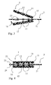
- Figure 3 is a cross-sectional view of a connector device shown in a position suitable for engaging with an electronic card.
- Figure 4 is a representation of the assembly of figure 3, in closed position with connection being engaged.
- Figures 5a and 5b show side view and front view schematic representations of a second exemplary embodiment of the connector device of the present invention.
- According to the scheme represented in figure 1, a
connector device 1 is shown having twoconnector members connection members connection points 13, made of electrically conductor material, such as for example copper, installed on selected areas on the surface of theconnection members assembly element 15 which will be described further below. - Although in the example of figure 1, both
connection members connection points 13, it is to be understood that theconnector device 1 of the invention may also be made withconnection points 13 installed only on one of theconnection members - The
connection points 13 are further connected to the end of acable 14 in any known manner. Thecable 14 may have a plurality of conductive wires. In practice the connector device of the invention may have the conductive wires already connected thereon before it is installed on an electronic card or fixed on a wall of a shelf. - Figure 2 shows an
electronic card 2, which in this example may be a PCB, having abase plate 21 upon which electronic components and other elements are installed. On a surface of the PCB, or on both front and rear surfaces thereof,connection pads 22 are installed. Theseconnection pads 2 may be installed at selected edges of the PCB and other conventional connection elements such as connectors or pads may be installed at other edges of the PCB as represented in figure 2 byreference numeral 25. Theconventional connection elements 25 may be used for connection in known manners for example to a back-plane of a shelf. - In figure 2, a
front surface 23 of the PCB is shown to have two rows ofconnection pads 22 installed on the upper and lower sides of the PCB. Likewise,connection pads 22 may be installed on therear surface 24 of the PCB.Connection pads 22 on bothsurfaces connection pads 22 may be made of any conductive material such as for example copper. - The two
connection members connection members - The assembly of the two
connection members assembly element 15 such that the assembly element permits one, or the two connection members, to be rotated around the axis of theassembly element 15 with respect to each other or with respect to theassembly element 15. Theassembly element 15 is in fact installed on the connection members and not on any external supporting piece such as for example the wall of a shelf, which is the case for some known connector devices with moveable connection elements. The fact that theassembly element 15 is installed on the connection member has the advantage that in this manner the connector device is made autonomous in the sense that it is capable of being used without a need to be first fixed in place. The connector device of the invention is capable of being already connected to thecable 14, for example in manufacturing stage or at any other moment before being installed on the wall of a shelf. - Another advantage of the fact that the connector device is made autonomous is that it may be easily removed from the position of connection on an electronic card in order to be left at a convenient storage place within the shelf until a time when further use is required and thus it is put back in connection with an electronic card, or simply it may be removed from one electronic card and connected on another electronic card inside the shelf.
- In the example of the embodiment of figures 1, 3 and 4 the
assembly element 15 is assumed to be made by means of a hinge installed at a respective end of each of the twoconnection members connection members hinge 15 for opening and closing of the assembly of theconnection members electronic card 2 to or from the assembly. In figure 3, the assembly of the twoconnection members hinge 15, and anelectronic card 2 is shown to be inserted inside the assembly. - Figure 4 shows a situation where the two
connection members electronic card 2 is placed inside the assembly. Theassembly element 15 may be such that each of theconnection members connection members assembly element 15, in which case one can assume that one connection member rotates with respect to the other - fixed - member. - In order to maintain the connection points 13 in permanent contact with
connection pads 22 of theelectronic cards 2, the assembly of the twoconnection members - In the closed position as shown in figure 4, the connection points 13 of the
connector device 1 enter in physical contact with theconnection pads 22 of theelectronic card 2 thus ensuring electrical connectivity there-between. The assembly may then be locked by means of the locking means 16. - In locked position, the
connector device 1 and theelectronic card 2 remain attached to each other due to the locking action of the locking means 16. However, should there be a need for a more secure attachment of theconnector device 1 to theelectronic card 2, additional fixing means may be employed (not shown) by means of any known fixing structure such as clips, screws, adhesive material or the like in order to ensure a stronger hold between theconnector device 1 and theelectronic card 2. - As shown in figures 3 and 4 the position of the connection points 13 and that of the
connection pads 22 are determined in conformity to each other such that by simple closing action exercised on theconnection member connection pads 22. This conformity in positioning is achieved by adequate layout design of each unit. Furthermore, as described above, theelectronic card 2 may haveconnection pads 22 installed only on one surface,front 23 or rear 24 thereof. In such case, theconnector device 1 may haveconnection points 13 installed only on theconnection member electronic pads 22 are installed. - In this manner, the solution proposed by the present invention provides the possibility of easily accessing to the connection points 13 in case of need, for example for soldering or cleaning the connection points 13. Another advantage of the connection device of the present invention is that in case the connector need to be removed from one card and connected to another, or kept unconnected, this can be done by simply opening the connector device and removing it from the place it was connected without any change in the position of the electronic card.
- Figures 5a and 5b show schematic representations in front and side view of an alternative embodiment of the connector device of the present invention in which like elements have been given like reference numerals. Thus the
connector device 1 of figures 5a and 5b has twoconnection members connection members Cable 14, which as shown in the figure may be comprised of a plurality of wires is connected to theconnection members 11, 12 (however in practice it is possible to have the cable connected to only one of the connection members). - The
connection members assembly members connection members connection members assembly members connection members third assembly member 15c is also shown in figures 5a and 5b. Thisthird assembly member 15c is capable of moving upward and downward as shown by an arrow. The shape of the third assembly element is designed such that when it moves in downward direction, a head portion thereof enters into a space in-between the twoconnection members - When the two
connection members electronic card 2 enter in-between theconnection members electronic card 2 is entered in-between the two connection members in such a way that theconnection pads 22 of the electronic card are in a position which is in conformity with the connection points 13. - Once the
electronic card 2 is inserted in place, thethird assembly member 15c is made to move outward (upward in figures 5a and 5b) from its position in-between the twoconnection members connection members connection members connection pads 22 of theelectronic card 2. The movement of the twoconnection members assembly members connection member respective assembly members - The movement of the
third assembly member 15c may be performed by any known means. For example, theassembly member 15c may be made to move up and down in a guiding structure such a sliding rail. Alternatively, the assembly element may be made to rotate around a fixed axis located at one side of the connector device. - In this embodiment also, locking means may be provided by any known means in order to maintain the whole structure secure as long as the connector device in maintained in contact with the electronic card.
- The connector device of the present invention, in any of its embodiments, is capable of being fixed, on a supporting surface, such as for example the wall of a shelf. As already discussed above, an advantage of the connector device of the invention is that cables may be installed thereupon before it being fixed on a supporting surface. Once the cable is connected, the connector may be fixed, permanently or provisionally, on a supporting surface and it may be connected to an electronic card at any desired time. The fixing may be made by any known means such as for example screws and knots.
- It is to be noted that the above embodiments are only examples of possible realizations of the solution of the present invention. The invention is not to be construed as being limited to these embodiment. In particular all known manners in which the connection members may be moved away and toward each other are included within the scope of the present invention.
Claims (7)
- A connector device (1) for providing electrical connection between a cable (14) and an electronic card (2) adapted for being installed in a shelf, the connector device (1) comprising two connection members (11, 12), at least one of said connection members having connection points (13) arranged at selected positions on a respective surface thereof, the two connection members (11, 12) being assembled together by means of an assembly element (15, 15a, 15b, 15c), the assembly of the two connection members (11,12) being adapted to have an open position suitable for allowing entry of an electronic card (2) between the two connection members and a closed position suitable for allowing electrical contact between the connection points (13) of the connector device and respective connection pads (22) of the electronic card, characterized in that said open position and said closed position are obtained independently of the position of the connector device with respect to the shelf and the electronic card, and in that the connector device (1) is capable of being moved from one position with respect to the shelf to another position while having the cable (14) connected thereon.
- A connector device according claim 1, wherein the assembly element (15) is installed on the connection members (11, 12).
- A connector device according to any one of the previous claims wherein the assembly element (15) is adapted for allowing rotation of one or both connection members (11, 12) with respect to the assembly element (15) and/or to each other.
- A connector element according to claim 3 wherein the assembly element is a hinge.
- A connector device according to any one of the claims 1 or 2 wherein the assembly element comprises two assembly members (15a, 15b) and is adapted for allowing a side-way movement of one or both connection members (11, 12) with respect to each other within the assembly members (15a, 15b).
- A connector device according to claim 5 wherein a third assembly member (15c) is adapted for forcing the one or both connection members (11, 12) to perform the side-way movement of one or both connection members (11, 12).
- A connector device according to any one of the previous claims, wherein the connector device comprises locking means (16) adapted for locking and unlocking the assembly of the two connection members (11, 12) together when the latter are in closed position.
Priority Applications (5)
| Application Number | Priority Date | Filing Date | Title |
|---|---|---|---|
| DE602005009385T DE602005009385D1 (en) | 2005-12-20 | 2005-12-20 | connector assembly |
| EP05301086A EP1801923B1 (en) | 2005-12-20 | 2005-12-20 | Connector device |
| ES05301086T ES2313257T3 (en) | 2005-12-20 | 2005-12-20 | CONNECTOR DEVICE. |
| AT05301086T ATE406675T1 (en) | 2005-12-20 | 2005-12-20 | CONNECTOR ARRANGEMENT |
| PCT/EP2006/068875 WO2007071524A1 (en) | 2005-12-20 | 2006-11-24 | Connector device |
Applications Claiming Priority (1)
| Application Number | Priority Date | Filing Date | Title |
|---|---|---|---|
| EP05301086A EP1801923B1 (en) | 2005-12-20 | 2005-12-20 | Connector device |
Publications (2)
| Publication Number | Publication Date |
|---|---|
| EP1801923A1 true EP1801923A1 (en) | 2007-06-27 |
| EP1801923B1 EP1801923B1 (en) | 2008-08-27 |
Family
ID=35732489
Family Applications (1)
| Application Number | Title | Priority Date | Filing Date |
|---|---|---|---|
| EP05301086A Expired - Lifetime EP1801923B1 (en) | 2005-12-20 | 2005-12-20 | Connector device |
Country Status (5)
| Country | Link |
|---|---|
| EP (1) | EP1801923B1 (en) |
| AT (1) | ATE406675T1 (en) |
| DE (1) | DE602005009385D1 (en) |
| ES (1) | ES2313257T3 (en) |
| WO (1) | WO2007071524A1 (en) |
Citations (2)
| Publication number | Priority date | Publication date | Assignee | Title |
|---|---|---|---|---|
| GB948391A (en) * | 1960-11-04 | 1964-02-05 | Bendix Corp | Electrical connector |
| WO1998034298A1 (en) * | 1997-01-31 | 1998-08-06 | The Whitaker Corporation | Connector for edge of pcb |
-
2005
- 2005-12-20 DE DE602005009385T patent/DE602005009385D1/en not_active Expired - Fee Related
- 2005-12-20 AT AT05301086T patent/ATE406675T1/en not_active IP Right Cessation
- 2005-12-20 EP EP05301086A patent/EP1801923B1/en not_active Expired - Lifetime
- 2005-12-20 ES ES05301086T patent/ES2313257T3/en not_active Expired - Lifetime
-
2006
- 2006-11-24 WO PCT/EP2006/068875 patent/WO2007071524A1/en not_active Ceased
Patent Citations (2)
| Publication number | Priority date | Publication date | Assignee | Title |
|---|---|---|---|---|
| GB948391A (en) * | 1960-11-04 | 1964-02-05 | Bendix Corp | Electrical connector |
| WO1998034298A1 (en) * | 1997-01-31 | 1998-08-06 | The Whitaker Corporation | Connector for edge of pcb |
Also Published As
| Publication number | Publication date |
|---|---|
| DE602005009385D1 (en) | 2008-10-09 |
| EP1801923B1 (en) | 2008-08-27 |
| ES2313257T3 (en) | 2009-03-01 |
| ATE406675T1 (en) | 2008-09-15 |
| WO2007071524A1 (en) | 2007-06-28 |
Similar Documents
| Publication | Publication Date | Title |
|---|---|---|
| EP0425192B1 (en) | Printed circuit board interconnect apparatus | |
| US7874869B2 (en) | Reconfigurable patch panel | |
| US7292457B2 (en) | Folding latching mechanism | |
| US4134631A (en) | Modular plug board system | |
| US7649751B2 (en) | Apparatus for inexpensive mezzanine-type card board-to-board connector blind mate alignment system using printed circuit board material | |
| US20170086324A1 (en) | System and method for housing circuit boards of different physical dimensions | |
| JPH06168062A (en) | Docking connector | |
| US8536454B2 (en) | Housing system for receptacles | |
| US10274998B2 (en) | Holding component, support component and assembly | |
| US6946602B1 (en) | Quadrifold housing assembly for electronics | |
| JP6367438B2 (en) | Modular server | |
| US8456857B2 (en) | Backplane for an electronic mounting rack | |
| US8830682B2 (en) | Electrical connection device and electronic device including the same | |
| US6926548B2 (en) | Circuit card | |
| TWI789383B (en) | Braille terminal and module for a braille terminal | |
| US4155109A (en) | Planar board and card-on-board electronic package assembly | |
| US11672098B2 (en) | Electronic device configured to be mounted in a cluster housing and comprising a front tray for mounting at least one expansion card | |
| US6338650B1 (en) | Rotatable card connector | |
| EP1801923B1 (en) | Connector device | |
| US6437992B1 (en) | Hot pluggable printed circuit board insulating system and method | |
| CN213545165U (en) | Adapter assembly of expansion card and computing system | |
| US7042239B1 (en) | Arrangement for manual disengagement of a device interface board from a personal tester | |
| US12526949B2 (en) | Cabled OCP connector | |
| US6814607B1 (en) | Apparatus and method for guiding and aligning circuit board assemblies to a backplane | |
| US20260075737A1 (en) | M.2 edge connector module |
Legal Events
| Date | Code | Title | Description |
|---|---|---|---|
| PUAI | Public reference made under article 153(3) epc to a published international application that has entered the european phase |
Free format text: ORIGINAL CODE: 0009012 |
|
| AK | Designated contracting states |
Kind code of ref document: A1 Designated state(s): AT BE BG CH CY CZ DE DK EE ES FI FR GB GR HU IE IS IT LI LT LU LV MC NL PL PT RO SE SI SK TR |
|
| AX | Request for extension of the european patent |
Extension state: AL BA HR MK YU |
|
| 17P | Request for examination filed |
Effective date: 20071227 |
|
| GRAP | Despatch of communication of intention to grant a patent |
Free format text: ORIGINAL CODE: EPIDOSNIGR1 |
|
| AKX | Designation fees paid |
Designated state(s): AT BE BG CH CY CZ DE DK EE ES FI FR GB GR HU IE IS IT LI LT LU LV MC NL PL PT RO SE SI SK TR |
|
| GRAS | Grant fee paid |
Free format text: ORIGINAL CODE: EPIDOSNIGR3 |
|
| GRAA | (expected) grant |
Free format text: ORIGINAL CODE: 0009210 |
|
| AK | Designated contracting states |
Kind code of ref document: B1 Designated state(s): AT BE BG CH CY CZ DE DK EE ES FI FR GB GR HU IE IS IT LI LT LU LV MC NL PL PT RO SE SI SK TR |
|
| REG | Reference to a national code |
Ref country code: GB Ref legal event code: FG4D |
|
| REG | Reference to a national code |
Ref country code: CH Ref legal event code: EP |
|
| REG | Reference to a national code |
Ref country code: IE Ref legal event code: FG4D |
|
| REF | Corresponds to: |
Ref document number: 602005009385 Country of ref document: DE Date of ref document: 20081009 Kind code of ref document: P |
|
| PG25 | Lapsed in a contracting state [announced via postgrant information from national office to epo] |
Ref country code: NL Free format text: LAPSE BECAUSE OF FAILURE TO SUBMIT A TRANSLATION OF THE DESCRIPTION OR TO PAY THE FEE WITHIN THE PRESCRIBED TIME-LIMIT Effective date: 20080827 Ref country code: IS Free format text: LAPSE BECAUSE OF FAILURE TO SUBMIT A TRANSLATION OF THE DESCRIPTION OR TO PAY THE FEE WITHIN THE PRESCRIBED TIME-LIMIT Effective date: 20081227 Ref country code: LT Free format text: LAPSE BECAUSE OF FAILURE TO SUBMIT A TRANSLATION OF THE DESCRIPTION OR TO PAY THE FEE WITHIN THE PRESCRIBED TIME-LIMIT Effective date: 20080827 |
|
| PG25 | Lapsed in a contracting state [announced via postgrant information from national office to epo] |
Ref country code: SI Free format text: LAPSE BECAUSE OF FAILURE TO SUBMIT A TRANSLATION OF THE DESCRIPTION OR TO PAY THE FEE WITHIN THE PRESCRIBED TIME-LIMIT Effective date: 20080827 Ref country code: LV Free format text: LAPSE BECAUSE OF FAILURE TO SUBMIT A TRANSLATION OF THE DESCRIPTION OR TO PAY THE FEE WITHIN THE PRESCRIBED TIME-LIMIT Effective date: 20080827 Ref country code: FI Free format text: LAPSE BECAUSE OF FAILURE TO SUBMIT A TRANSLATION OF THE DESCRIPTION OR TO PAY THE FEE WITHIN THE PRESCRIBED TIME-LIMIT Effective date: 20080827 Ref country code: AT Free format text: LAPSE BECAUSE OF FAILURE TO SUBMIT A TRANSLATION OF THE DESCRIPTION OR TO PAY THE FEE WITHIN THE PRESCRIBED TIME-LIMIT Effective date: 20080827 |
|
| PGFP | Annual fee paid to national office [announced via postgrant information from national office to epo] |
Ref country code: ES Payment date: 20081219 Year of fee payment: 4 |
|
| REG | Reference to a national code |
Ref country code: ES Ref legal event code: FG2A Ref document number: 2313257 Country of ref document: ES Kind code of ref document: T3 |
|
| PG25 | Lapsed in a contracting state [announced via postgrant information from national office to epo] |
Ref country code: BE Free format text: LAPSE BECAUSE OF FAILURE TO SUBMIT A TRANSLATION OF THE DESCRIPTION OR TO PAY THE FEE WITHIN THE PRESCRIBED TIME-LIMIT Effective date: 20080827 |
|
| PG25 | Lapsed in a contracting state [announced via postgrant information from national office to epo] |
Ref country code: DK Free format text: LAPSE BECAUSE OF FAILURE TO SUBMIT A TRANSLATION OF THE DESCRIPTION OR TO PAY THE FEE WITHIN THE PRESCRIBED TIME-LIMIT Effective date: 20080827 Ref country code: BG Free format text: LAPSE BECAUSE OF FAILURE TO SUBMIT A TRANSLATION OF THE DESCRIPTION OR TO PAY THE FEE WITHIN THE PRESCRIBED TIME-LIMIT Effective date: 20081127 |
|
| PGFP | Annual fee paid to national office [announced via postgrant information from national office to epo] |
Ref country code: FR Payment date: 20081220 Year of fee payment: 4 |
|
| PG25 | Lapsed in a contracting state [announced via postgrant information from national office to epo] |
Ref country code: RO Free format text: LAPSE BECAUSE OF FAILURE TO SUBMIT A TRANSLATION OF THE DESCRIPTION OR TO PAY THE FEE WITHIN THE PRESCRIBED TIME-LIMIT Effective date: 20080827 Ref country code: SK Free format text: LAPSE BECAUSE OF FAILURE TO SUBMIT A TRANSLATION OF THE DESCRIPTION OR TO PAY THE FEE WITHIN THE PRESCRIBED TIME-LIMIT Effective date: 20080827 Ref country code: CZ Free format text: LAPSE BECAUSE OF FAILURE TO SUBMIT A TRANSLATION OF THE DESCRIPTION OR TO PAY THE FEE WITHIN THE PRESCRIBED TIME-LIMIT Effective date: 20080827 Ref country code: PT Free format text: LAPSE BECAUSE OF FAILURE TO SUBMIT A TRANSLATION OF THE DESCRIPTION OR TO PAY THE FEE WITHIN THE PRESCRIBED TIME-LIMIT Effective date: 20090127 |
|
| PGFP | Annual fee paid to national office [announced via postgrant information from national office to epo] |
Ref country code: DE Payment date: 20081219 Year of fee payment: 4 |
|
| PLBE | No opposition filed within time limit |
Free format text: ORIGINAL CODE: 0009261 |
|
| STAA | Information on the status of an ep patent application or granted ep patent |
Free format text: STATUS: NO OPPOSITION FILED WITHIN TIME LIMIT |
|
| PG25 | Lapsed in a contracting state [announced via postgrant information from national office to epo] |
Ref country code: MC Free format text: LAPSE BECAUSE OF NON-PAYMENT OF DUE FEES Effective date: 20081231 Ref country code: EE Free format text: LAPSE BECAUSE OF FAILURE TO SUBMIT A TRANSLATION OF THE DESCRIPTION OR TO PAY THE FEE WITHIN THE PRESCRIBED TIME-LIMIT Effective date: 20080827 |
|
| 26N | No opposition filed |
Effective date: 20090528 |
|
| REG | Reference to a national code |
Ref country code: IE Ref legal event code: MM4A |
|
| PG25 | Lapsed in a contracting state [announced via postgrant information from national office to epo] |
Ref country code: IE Free format text: LAPSE BECAUSE OF NON-PAYMENT OF DUE FEES Effective date: 20081220 |
|
| PGFP | Annual fee paid to national office [announced via postgrant information from national office to epo] |
Ref country code: IT Payment date: 20081231 Year of fee payment: 4 |
|
| PG25 | Lapsed in a contracting state [announced via postgrant information from national office to epo] |
Ref country code: SE Free format text: LAPSE BECAUSE OF FAILURE TO SUBMIT A TRANSLATION OF THE DESCRIPTION OR TO PAY THE FEE WITHIN THE PRESCRIBED TIME-LIMIT Effective date: 20081127 |
|
| PG25 | Lapsed in a contracting state [announced via postgrant information from national office to epo] |
Ref country code: PL Free format text: LAPSE BECAUSE OF FAILURE TO SUBMIT A TRANSLATION OF THE DESCRIPTION OR TO PAY THE FEE WITHIN THE PRESCRIBED TIME-LIMIT Effective date: 20080827 |
|
| PG25 | Lapsed in a contracting state [announced via postgrant information from national office to epo] |
Ref country code: HU Free format text: LAPSE BECAUSE OF FAILURE TO SUBMIT A TRANSLATION OF THE DESCRIPTION OR TO PAY THE FEE WITHIN THE PRESCRIBED TIME-LIMIT Effective date: 20090228 Ref country code: CY Free format text: LAPSE BECAUSE OF FAILURE TO SUBMIT A TRANSLATION OF THE DESCRIPTION OR TO PAY THE FEE WITHIN THE PRESCRIBED TIME-LIMIT Effective date: 20080827 Ref country code: LU Free format text: LAPSE BECAUSE OF NON-PAYMENT OF DUE FEES Effective date: 20081220 |
|
| REG | Reference to a national code |
Ref country code: CH Ref legal event code: PL |
|
| GBPC | Gb: european patent ceased through non-payment of renewal fee |
Effective date: 20091220 |
|
| PG25 | Lapsed in a contracting state [announced via postgrant information from national office to epo] |
Ref country code: TR Free format text: LAPSE BECAUSE OF FAILURE TO SUBMIT A TRANSLATION OF THE DESCRIPTION OR TO PAY THE FEE WITHIN THE PRESCRIBED TIME-LIMIT Effective date: 20080827 |
|
| REG | Reference to a national code |
Ref country code: FR Ref legal event code: ST Effective date: 20100831 |
|
| PG25 | Lapsed in a contracting state [announced via postgrant information from national office to epo] |
Ref country code: LI Free format text: LAPSE BECAUSE OF NON-PAYMENT OF DUE FEES Effective date: 20091231 Ref country code: FR Free format text: LAPSE BECAUSE OF NON-PAYMENT OF DUE FEES Effective date: 20091231 Ref country code: CH Free format text: LAPSE BECAUSE OF NON-PAYMENT OF DUE FEES Effective date: 20091231 |
|
| PG25 | Lapsed in a contracting state [announced via postgrant information from national office to epo] |
Ref country code: DE Free format text: LAPSE BECAUSE OF NON-PAYMENT OF DUE FEES Effective date: 20100701 |
|
| PG25 | Lapsed in a contracting state [announced via postgrant information from national office to epo] |
Ref country code: GB Free format text: LAPSE BECAUSE OF NON-PAYMENT OF DUE FEES Effective date: 20091220 |
|
| REG | Reference to a national code |
Ref country code: ES Ref legal event code: FD2A Effective date: 20110304 |
|
| PG25 | Lapsed in a contracting state [announced via postgrant information from national office to epo] |
Ref country code: IT Free format text: LAPSE BECAUSE OF NON-PAYMENT OF DUE FEES Effective date: 20091220 |
|
| PG25 | Lapsed in a contracting state [announced via postgrant information from national office to epo] |
Ref country code: ES Free format text: LAPSE BECAUSE OF NON-PAYMENT OF DUE FEES Effective date: 20110303 Ref country code: GR Free format text: LAPSE BECAUSE OF NON-PAYMENT OF DUE FEES Effective date: 20081231 |
|
| PG25 | Lapsed in a contracting state [announced via postgrant information from national office to epo] |
Ref country code: ES Free format text: LAPSE BECAUSE OF NON-PAYMENT OF DUE FEES Effective date: 20091221 |
|
| REG | Reference to a national code |
Ref country code: FR Ref legal event code: CA Effective date: 20150521 |
|
| REG | Reference to a national code |
Ref country code: FR Ref legal event code: CA Effective date: 20150521 |