EP1801864A1 - Method for selective epitaxial growth of source/drain areas - Google Patents
Method for selective epitaxial growth of source/drain areas Download PDFInfo
- Publication number
- EP1801864A1 EP1801864A1 EP05447290A EP05447290A EP1801864A1 EP 1801864 A1 EP1801864 A1 EP 1801864A1 EP 05447290 A EP05447290 A EP 05447290A EP 05447290 A EP05447290 A EP 05447290A EP 1801864 A1 EP1801864 A1 EP 1801864A1
- Authority
- EP
- European Patent Office
- Prior art keywords
- poly
- substrate
- area
- top layer
- epitaxial growth
- Prior art date
- Legal status (The legal status is an assumption and is not a legal conclusion. Google has not performed a legal analysis and makes no representation as to the accuracy of the status listed.)
- Granted
Links
Images


Classifications
-
- H—ELECTRICITY
- H10—SEMICONDUCTOR DEVICES; ELECTRIC SOLID-STATE DEVICES NOT OTHERWISE PROVIDED FOR
- H10D—INORGANIC ELECTRIC SEMICONDUCTOR DEVICES
- H10D84/00—Integrated devices formed in or on semiconductor substrates that comprise only semiconducting layers, e.g. on Si wafers or on GaAs-on-Si wafers
- H10D84/01—Manufacture or treatment
- H10D84/0123—Integrating together multiple components covered by H10D12/00 or H10D30/00, e.g. integrating multiple IGBTs
- H10D84/0126—Integrating together multiple components covered by H10D12/00 or H10D30/00, e.g. integrating multiple IGBTs the components including insulated gates, e.g. IGFETs
- H10D84/0165—Integrating together multiple components covered by H10D12/00 or H10D30/00, e.g. integrating multiple IGBTs the components including insulated gates, e.g. IGFETs the components including complementary IGFETs, e.g. CMOS devices
- H10D84/017—Manufacturing their source or drain regions, e.g. silicided source or drain regions
-
- H—ELECTRICITY
- H10—SEMICONDUCTOR DEVICES; ELECTRIC SOLID-STATE DEVICES NOT OTHERWISE PROVIDED FOR
- H10D—INORGANIC ELECTRIC SEMICONDUCTOR DEVICES
- H10D62/00—Semiconductor bodies, or regions thereof, of devices having potential barriers
- H10D62/01—Manufacture or treatment
- H10D62/021—Forming source or drain recesses by etching e.g. recessing by etching and then refilling
-
- H—ELECTRICITY
- H10—SEMICONDUCTOR DEVICES; ELECTRIC SOLID-STATE DEVICES NOT OTHERWISE PROVIDED FOR
- H10D—INORGANIC ELECTRIC SEMICONDUCTOR DEVICES
- H10D84/00—Integrated devices formed in or on semiconductor substrates that comprise only semiconducting layers, e.g. on Si wafers or on GaAs-on-Si wafers
- H10D84/01—Manufacture or treatment
- H10D84/02—Manufacture or treatment characterised by using material-based technologies
- H10D84/03—Manufacture or treatment characterised by using material-based technologies using Group IV technology, e.g. silicon technology or silicon-carbide [SiC] technology
- H10D84/038—Manufacture or treatment characterised by using material-based technologies using Group IV technology, e.g. silicon technology or silicon-carbide [SiC] technology using silicon technology, e.g. SiGe
-
- Y—GENERAL TAGGING OF NEW TECHNOLOGICAL DEVELOPMENTS; GENERAL TAGGING OF CROSS-SECTIONAL TECHNOLOGIES SPANNING OVER SEVERAL SECTIONS OF THE IPC; TECHNICAL SUBJECTS COVERED BY FORMER USPC CROSS-REFERENCE ART COLLECTIONS [XRACs] AND DIGESTS
- Y10—TECHNICAL SUBJECTS COVERED BY FORMER USPC
- Y10S—TECHNICAL SUBJECTS COVERED BY FORMER USPC CROSS-REFERENCE ART COLLECTIONS [XRACs] AND DIGESTS
- Y10S438/00—Semiconductor device manufacturing: process
- Y10S438/914—Doping
- Y10S438/924—To facilitate selective etching
Definitions
- the present invention relates to a method for the selective growth of an epitaxial layer on source/drain areas.
- HM hard mask
- the hardmask usually has to be removed afterwards.
- an etch resistant material is employed for the hardmask.
- a gate stack is formed, which is capped with a silicon oxide and with spacers (see Fig.1A). Spacers around the gate are typically in Si nitride. The full encapsulation is of vital importance, as it protects the gate during epitaxial growth. Further processing steps are depicted in Fig. 1. In a first step either a single layer hardmask is deposited (Fig.1B.1)) or a hardmask stack, which cannot be etched during source/drain etching (Fig. 1B.2) a two-layer stack is shown). Next a first area is opened up comprising a source and drain (S/D) and a gate stack (Fig.1C).
- S/D source and drain
- Fig.1C gate stack
- the hardmask (HM) is etched selectively towards Si oxide (used to cap the gate) and Si nitride (used for the spacers) of the first area and also selectively to the hardmask on top of a second area of the substrate. If the hardmask etching is not performed in a sufficiently selective way, an accurate control of the lost amount of Si oxide/Si nitride is required.
- a source/drain (S/D) silicon etch is performed selectively towards Si oxide and Si nitride. The etch rate depends on the amount of exposed Si. A part of the hardmask is consumed by a break through (BT) etch. Next an epitaxial layer is grown.
- Silicon nitride is the typical material for spacers. Si nitride cannot be applied for the hardmask, as during hardmask removal it would remove said spacers as well.
- An alternative would be the use of Si oxide.
- Si oxide is not an appropriate material either, as Si oxide may be used on top of the gate.
- Si oxide hardmask one would have to remove the hardmask very carefully in order not to damage the oxide capping layer on top of the gate (in order to protect said gate during the epitaxial growth).
- Using a Si oxide hardmask the extra oxide on top of the second area must be removed, which increases field loss on the first area, as the latter 'sees' the double removal of the oxide layer.
- An option would be to use lithography and etch only on the second area, which increases complexity.
- poly-silicon as the hardmask material.
- the poly-Si hardmask would have to be removed before the epitaxial growth, as it does not allow such epitaxial growth in a selective way.
- the epitaxial layer will cover the whole wafer and not only fill the S/D areas of the first area.
- it would be desirable and advantageous to have a poly-Si hardmask as it would allow etching selectively towards nitride and oxide (e.g. towards an oxide gate capping layer or towards the field oxide), which would put less strain.
- the present invention aims to provide a method for selective epitaxial growth of S/D areas that overcomes the drawbacks of the prior art solutions.
- the present invention relates to a method for selective epitaxial growth of source/drain areas. It comprises an initial step of providing a substrate of semiconductor material, said substrate consisting of a first substrate area and a second substrate area. The first area comprises at least one gate stack. The method further comprises the steps of :
- a second layer is applied between the poly-Si top layer and the substrate, which is not etchable with the given etch chemistry.
- the step of removing the poly-Si top layer from the first area is performed until a spacer liner, a spacer material or said second layer is exposed.
- the step of simultaneously removing comprises a break through etch step for removing the spacer liner or the second layer.
- a step is performed of removing resist on top of the second area.
- the second area comprises at least one gate stack.
- the method further comprises a step of end-point triggering.
- the substrate is preferably of silicon, germanium, SiGe or any other suitable semiconductor material.
- the given etch chemistry is preferably of a mixture of SF 6 and HBr. Any other etch chemistry suitable for etching S/D areas selectively towards Si oxide and Si nitride may also be used.
- the second layer is preferably of oxide.
- it may be of nitride.
- Fig. 1 represents the method steps of the prior art solution.
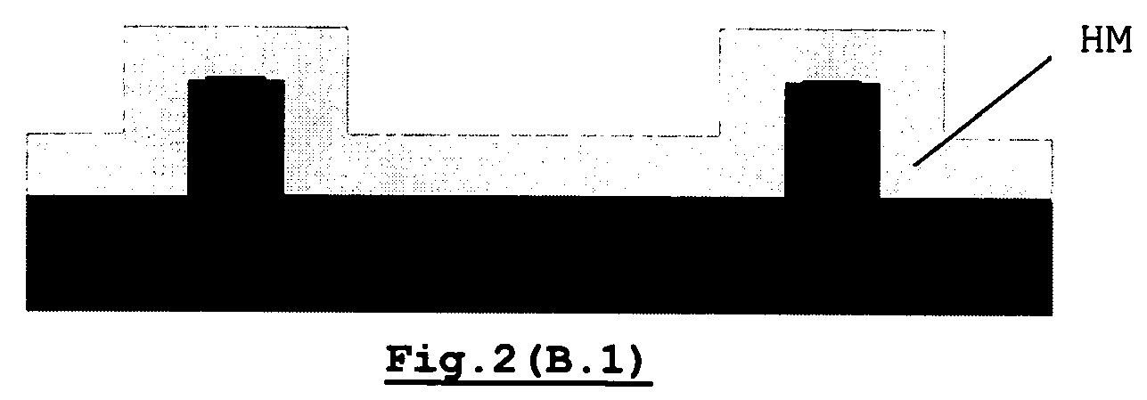
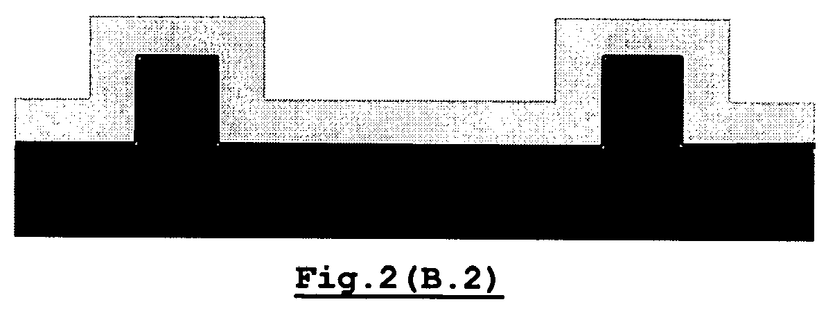
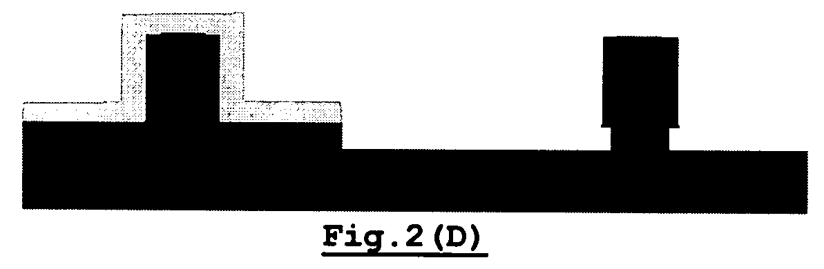
- Fig. 2 represents the method steps of the solution according to the present invention.
- the method according to the present invention combines a selective epitaxial growth of S/D areas with the advantageous use of a hardmask etchable with the same etch chemistry as the S/D material to be etched.
- a preferable example is a poly-Si hardmask.
- it is (poly-) SiGe.
- a gate stack is fully encapsulated after spacer processing (Fig.2(A)). Then the different steps of the method are performed as presented in the rest of Fig.2.
- a poly-Si or a poly-SiGe hardmask layer (Fig.2(B.1)) or a hardmask layer stack (Fig.2(B.2)) comprising at least a poly-Si or poly-SiGe top layer and e.g. a further layer of oxide is deposited.
- the hardmask top layer must be such that it is selectively etchable towards Si oxide (e.g. on top of the gate) and Si nitride. The top layer is thus etchable with a chemistry that does not etch e.g. the Si oxide on top of the gate.
- a first area on the substrate is opened up by removing the top layer, stopping on the spacer material and spacer liner (or on an extra deposited material in case of a masking material stack).
- the top layer on the second area remains unchanged at this stage.
- the resist on top of the second area is removed by means of a resist strip.
- a subsequent step the poly-Si or poly-SiGe top layer on the second area as well as a part of the substrate in the first area are etched with said given solution.
- This step may comprise the application of a BT etch step, wherein the remaining spacer liner or a stop layer in extra deposited material is removed.
- the overall etch rate could decrease and as such the etch depth control would be improved.
- an end-point triggering can be performed, which was not possible in the prior art solutions, where no poly-Si or poly-SiGe hardmask was used.
- the end-point is defined as the time instant during an etching operation when etching of material is completed (or in this case when the transition from the poly-Si or poly-SiGe to Si oxide is detected) and continuing the etching would result in overetching. This transition may simultaneously be used as end-point detection for the S/D material etching.
- the exposed Si oxide liner or extra oxide which was deposited
- the etch rate of the hardmask material can be chosen to be the same/higher/lower in order to get an etch depth, which would be the same/lower/higher than the etch depth of the S/D material.
- the method according to the invention allows a better control of the etch rate (less pattern dependent for the recess etch in a S/D module). Further the thickness of the layer to which the etch is selective can be reduced, since it doesn't have to withstand the BT etch. The consumption of the field oxide can so be limited. As a further advantage opening up the HM on the first area can be more gentle on the Si oxide on top of the gate stack in the first area, which could reduce the thickness of the oxide needed on the gate.
Landscapes
- Insulated Gate Type Field-Effect Transistor (AREA)
- Metal-Oxide And Bipolar Metal-Oxide Semiconductor Integrated Circuits (AREA)
Abstract
- applying at least a poly-Si or poly-SiGe top layer on said substrate, said top layer being etchable with a given etch chemistry,
- removing said poly-Si or poly-SiGe top layer from said first area of said substrate selectively towards said poly-Si or poly-SiGe top layer in said second substrate area,
- removing simultaneously said poly-Si or poly-SiGe top layer on said second substrate area and at least a part of said substrate in said first substrate area with said given solution,
- performing a selective epitaxial growth of S/D areas in said first substrate area.


Description
- The present invention relates to a method for the selective growth of an epitaxial layer on source/drain areas.
- In semiconductor fabrication a hard mask (HM) is applied in order to protect part of the wafer from etching the other part of the wafer. The hardmask usually has to be removed afterwards. Typically an etch resistant material is employed for the hardmask.
- When considering a process flow for fabricating a CMOS FET transistor, a gate stack is formed, which is capped with a silicon oxide and with spacers (see Fig.1A). Spacers around the gate are typically in Si nitride. The full encapsulation is of vital importance, as it protects the gate during epitaxial growth. Further processing steps are depicted in Fig. 1. In a first step either a single layer hardmask is deposited (Fig.1B.1)) or a hardmask stack, which cannot be etched during source/drain etching (Fig. 1B.2) a two-layer stack is shown). Next a first area is opened up comprising a source and drain (S/D) and a gate stack (Fig.1C). The hardmask (HM) is etched selectively towards Si oxide (used to cap the gate) and Si nitride (used for the spacers) of the first area and also selectively to the hardmask on top of a second area of the substrate. If the hardmask etching is not performed in a sufficiently selective way, an accurate control of the lost amount of Si oxide/Si nitride is required. In the following step (Fig. 1D) a source/drain (S/D) silicon etch is performed selectively towards Si oxide and Si nitride. The etch rate depends on the amount of exposed Si. A part of the hardmask is consumed by a break through (BT) etch. Next an epitaxial layer is grown. During the epitaxial growth a selective growth towards the hardmask in the second area is required. The epitaxial growth is only selective towards Si oxide and Si nitride. Finally the hardmask is removed on the second area (Fig.1E). Note that the hardmask cannot be removed before the epitaxial layer has grown as it should protect (at least said second area on) the wafer. In the state of the art approach the hardmask on the second area is removed afterwards by an etching step, which causes field oxide loss. A possible solution exists in providing an additional protective mask on said first area, which clearly would increase the complexity.
- Silicon nitride is the typical material for spacers. Si nitride cannot be applied for the hardmask, as during hardmask removal it would remove said spacers as well. An alternative would be the use of Si oxide. However, Si oxide is not an appropriate material either, as Si oxide may be used on top of the gate. When using a Si oxide hardmask, one would have to remove the hardmask very carefully in order not to damage the oxide capping layer on top of the gate (in order to protect said gate during the epitaxial growth). Using a Si oxide hardmask, the extra oxide on top of the second area must be removed, which increases field loss on the first area, as the latter 'sees' the double removal of the oxide layer. An option would be to use lithography and etch only on the second area, which increases complexity.
- In the state of the art solutions it is neither possible to use poly-silicon as the hardmask material. The poly-Si hardmask would have to be removed before the epitaxial growth, as it does not allow such epitaxial growth in a selective way. The epitaxial layer will cover the whole wafer and not only fill the S/D areas of the first area. However, it would be desirable and advantageous to have a poly-Si hardmask, as it would allow etching selectively towards nitride and oxide (e.g. towards an oxide gate capping layer or towards the field oxide), which would put less strain.
- The present invention aims to provide a method for selective epitaxial growth of S/D areas that overcomes the drawbacks of the prior art solutions.
- The present invention relates to a method for selective epitaxial growth of source/drain areas. It comprises an initial step of providing a substrate of semiconductor material, said substrate consisting of a first substrate area and a second substrate area. The first area comprises at least one gate stack. The method further comprises the steps of :
- applying at least a poly-Si top layer on the substrate, said top layer being etchable with a given etch chemistry,
- removing the poly-Si top layer from the first area of the substrate selectively towards the poly-Si top layer in the second substrate area,
- removing simultaneously the poly-Si top layer on the second substrate area and at least a part of the substrate in the first substrate area with the given solution,
- performing a selective epitaxial growth of S/D areas in the first substrate area.
- In a preferred embodiment a second layer is applied between the poly-Si top layer and the substrate, which is not etchable with the given etch chemistry.
- Advantageously the step of removing the poly-Si top layer from the first area is performed until a spacer liner, a spacer material or said second layer is exposed.
- In a specific embodiment the step of simultaneously removing comprises a break through etch step for removing the spacer liner or the second layer.
- Between the step of removing the poly-Si top layer from the first area and the step of simultaneously removing preferably a step is performed of removing resist on top of the second area.
- In another embodiment the second area comprises at least one gate stack.
- In another advantageous embodiment the method further comprises a step of end-point triggering.
- The substrate is preferably of silicon, germanium, SiGe or any other suitable semiconductor material.
- The given etch chemistry is preferably of a mixture of SF6 and HBr. Any other etch chemistry suitable for etching S/D areas selectively towards Si oxide and Si nitride may also be used.
- The second layer is preferably of oxide. Optionally it may be of nitride.
- Fig. 1 represents the method steps of the prior art solution.
- Fig. 2 represents the method steps of the solution according to the present invention.
- The method according to the present invention combines a selective epitaxial growth of S/D areas with the advantageous use of a hardmask etchable with the same etch chemistry as the S/D material to be etched. A preferable example is a poly-Si hardmask. Optionally it is (poly-) SiGe. Typically, a gate stack is fully encapsulated after spacer processing (Fig.2(A)). Then the different steps of the method are performed as presented in the rest of Fig.2.
- First a poly-Si or a poly-SiGe hardmask layer (Fig.2(B.1)) or a hardmask layer stack (Fig.2(B.2)) comprising at least a poly-Si or poly-SiGe top layer and e.g. a further layer of oxide is deposited. The hardmask top layer must be such that it is selectively etchable towards Si oxide (e.g. on top of the gate) and Si nitride. The top layer is thus etchable with a chemistry that does not etch e.g. the Si oxide on top of the gate. When using a poly-Si or poly-SiGe HM approach, it is possible to etch the poly-Si or poly-SiGe selectively to Si oxide and Si nitride. This way less strain is put on the oxide on top of the gate.
- In a next step (Fig.2(C)) a first area on the substrate is opened up by removing the top layer, stopping on the spacer material and spacer liner (or on an extra deposited material in case of a masking material stack). The top layer on the second area remains unchanged at this stage.
- In an intermediate step the resist on top of the second area is removed by means of a resist strip.
- In a subsequent step (Fig.2(D)) the poly-Si or poly-SiGe top layer on the second area as well as a part of the substrate in the first area are etched with said given solution. This step may comprise the application of a BT etch step, wherein the remaining spacer liner or a stop layer in extra deposited material is removed. As the poly-Si or poly-SiGe hardmask is consumed during this process step, the overall etch rate could decrease and as such the etch depth control would be improved.
- During the poly-Si or poly-SiGe hardmask removal, an end-point triggering can be performed, which was not possible in the prior art solutions, where no poly-Si or poly-SiGe hardmask was used. The end-point is defined as the time instant during an etching operation when etching of material is completed (or in this case when the transition from the poly-Si or poly-SiGe to Si oxide is detected) and continuing the etching would result in overetching. This transition may simultaneously be used as end-point detection for the S/D material etching. The exposed Si oxide (liner or extra oxide which was deposited) has to sustain the pre-epi clean before epitaxial growth. The etch rate of the hardmask material can be chosen to be the same/higher/lower in order to get an etch depth, which would be the same/lower/higher than the etch depth of the S/D material.
- The method according to the invention allows a better control of the etch rate (less pattern dependent for the recess etch in a S/D module). Further the thickness of the layer to which the etch is selective can be reduced, since it doesn't have to withstand the BT etch. The consumption of the field oxide can so be limited. As a further advantage opening up the HM on the first area can be more gentle on the Si oxide on top of the gate stack in the first area, which could reduce the thickness of the oxide needed on the gate.
Claims (10)
- Method for selective epitaxial growth of source/drain (S/D) areas, comprising the step of providing a substrate of semiconductor material, said substrate consisting of a first substrate area and a second substrate area, said first area comprising at least one gate stack, characterised in that it further comprises the steps of :- applying at least a poly-Si or poly-SiGe top layer on said substrate, said top layer being etchable with a given etch chemistry,- removing said poly-Si or poly-SiGe top layer from said first area of said substrate selectively towards said poly-Si or poly-SiGe top layer in said second substrate area,- removing simultaneously said poly-Si or poly-SiGe top layer on said second substrate area and at least a part of said substrate in said first substrate area with said given solution,- performing a selective epitaxial growth of S/D areas in said first substrate area.
- Method for selective epitaxial growth as in claim 1, wherein between said poly-Si or poly-SiGe top layer and said substrate a second layer is applied, which is not etchable with said given etch chemistry.
- Method for selective epitaxial growth as in claim 1 or 2, wherein said step of removing said poly-Si or poly-SiGe top layer from said first area is performed until a spacer liner, a spacer material or said second layer is exposed.
- Method for selective epitaxial growth as in claim 3, wherein said step of simultaneously removing comprises a break through etch step for removing said spacer liner or said second layer.
- Method for selective epitaxial growth as in any of claims 1 to 4, wherein between said step of removing said poly-Si or poly-SiGe top layer from said first area and the step of simultaneously removing a step is performed of removing resist on top of said second area.
- Method as in any of the previous claims, wherein said second area comprises at least one gate stack.
- Method as in any of claims 1 to 6, further comprising a step of end-point triggering.
- Method as in any of the previous claims, wherein said substrate is of silicon, germanium or SiGe.
- Method as in any of the previous claims, wherein said given etch chemistry is a mixture of SF6 and HBr.
- Method as in any of the previous claims, wherein said second layer is of oxide.
Priority Applications (5)
| Application Number | Priority Date | Filing Date | Title |
|---|---|---|---|
| AT05447290T ATE449418T1 (en) | 2005-12-23 | 2005-12-23 | METHOD FOR SELECTIVE EPITACTIC GROWTH OF SOURCE/DRAIN AREAS |
| DE602005017806T DE602005017806D1 (en) | 2005-12-23 | 2005-12-23 | Method for selective epitaxial growth of source / drain regions |
| EP05447290A EP1801864B1 (en) | 2005-12-23 | 2005-12-23 | Method for selective epitaxial growth of source/drain areas |
| US11/645,149 US7799664B2 (en) | 2005-12-23 | 2006-12-22 | Method for selective epitaxial growth of source/drain areas |
| JP2006347125A JP2007227892A (en) | 2005-12-23 | 2006-12-25 | Method for selective epitaxial growth of source / drain regions |
Applications Claiming Priority (1)
| Application Number | Priority Date | Filing Date | Title |
|---|---|---|---|
| EP05447290A EP1801864B1 (en) | 2005-12-23 | 2005-12-23 | Method for selective epitaxial growth of source/drain areas |
Publications (2)
| Publication Number | Publication Date |
|---|---|
| EP1801864A1 true EP1801864A1 (en) | 2007-06-27 |
| EP1801864B1 EP1801864B1 (en) | 2009-11-18 |
Family
ID=36636404
Family Applications (1)
| Application Number | Title | Priority Date | Filing Date |
|---|---|---|---|
| EP05447290A Expired - Lifetime EP1801864B1 (en) | 2005-12-23 | 2005-12-23 | Method for selective epitaxial growth of source/drain areas |
Country Status (5)
| Country | Link |
|---|---|
| US (1) | US7799664B2 (en) |
| EP (1) | EP1801864B1 (en) |
| JP (1) | JP2007227892A (en) |
| AT (1) | ATE449418T1 (en) |
| DE (1) | DE602005017806D1 (en) |
Cited By (1)
| Publication number | Priority date | Publication date | Assignee | Title |
|---|---|---|---|---|
| US9583619B2 (en) | 2015-02-13 | 2017-02-28 | Shanghai Huali Microelectronics Corporation | Semiconductor devices with shaped cavities for embedding germanium material and manufacturing processes thereof |
Families Citing this family (7)
| Publication number | Priority date | Publication date | Assignee | Title |
|---|---|---|---|---|
| US8877596B2 (en) | 2010-06-24 | 2014-11-04 | International Business Machines Corporation | Semiconductor devices with asymmetric halo implantation and method of manufacture |
| CN103871902A (en) | 2014-03-24 | 2014-06-18 | 上海华力微电子有限公司 | Semiconductor treatment technology and semiconductor device preparation method |
| CN105869991B (en) | 2015-01-23 | 2018-05-11 | 上海华力微电子有限公司 | Method and system for the uniformity for improving SiGe thickness |
| CN105990172B (en) | 2015-01-30 | 2018-07-31 | 上海华力微电子有限公司 | The design of embedded SiGe extension testings block |
| CN104851884A (en) | 2015-04-14 | 2015-08-19 | 上海华力微电子有限公司 | Forming chamber for germanium and silicon filling material |
| CN104821336B (en) | 2015-04-20 | 2017-12-12 | 上海华力微电子有限公司 | For improving the method and system of device surface uniformity using conformal packed layer |
| CN105097554B (en) | 2015-08-24 | 2018-12-07 | 上海华力微电子有限公司 | For reducing the method and system of the dislocation defects in high concentration epitaxy technique |
Citations (1)
| Publication number | Priority date | Publication date | Assignee | Title |
|---|---|---|---|---|
| US20050158931A1 (en) * | 2003-08-04 | 2005-07-21 | Huajie Chen | Method of making strained semiconductor transistors having lattice-mismatched semiconductor regions underlying source and drain regions |
Family Cites Families (14)
| Publication number | Priority date | Publication date | Assignee | Title |
|---|---|---|---|---|
| JPS5242375A (en) * | 1975-09-30 | 1977-04-01 | Matsushita Electric Ind Co Ltd | Process for production of semiconductor device |
| JPS62120028A (en) * | 1985-11-20 | 1987-06-01 | Toshiba Corp | Etching method for semiconductor substrate |
| JPH0430518A (en) * | 1990-05-28 | 1992-02-03 | Fujitsu Ltd | Manufacture of semiconductor device |
| JPH04370929A (en) * | 1991-06-20 | 1992-12-24 | Sharp Corp | Dry etching method |
| JPH0864579A (en) * | 1994-08-23 | 1996-03-08 | Toshiba Corp | Method for manufacturing semiconductor device |
| US6632718B1 (en) * | 1998-07-15 | 2003-10-14 | Texas Instruments Incorporated | Disposable spacer technology for reduced cost CMOS processing |
| JP2000299462A (en) * | 1999-04-15 | 2000-10-24 | Toshiba Corp | Semiconductor device and manufacturing method thereof |
| JP2003109969A (en) * | 2001-09-28 | 2003-04-11 | Toshiba Corp | Semiconductor device and manufacturing method thereof |
| KR20030090411A (en) * | 2002-05-23 | 2003-11-28 | 삼성전자주식회사 | CMOS gate electrode using selective growth and fabrication method the same |
| US7303949B2 (en) * | 2003-10-20 | 2007-12-04 | International Business Machines Corporation | High performance stress-enhanced MOSFETs using Si:C and SiGe epitaxial source/drain and method of manufacture |
| US6872610B1 (en) * | 2003-11-18 | 2005-03-29 | Texas Instruments Incorporated | Method for preventing polysilicon mushrooming during selective epitaxial processing |
| JP2005197474A (en) * | 2004-01-07 | 2005-07-21 | Oki Electric Ind Co Ltd | Manufacturing method of semiconductor device |
| JP2006019577A (en) * | 2004-07-02 | 2006-01-19 | Fujitsu Ltd | Exposure mask and method of manufacturing semiconductor device |
| US7288802B2 (en) * | 2005-07-27 | 2007-10-30 | International Business Machines Corporation | Virtual body-contacted trigate |
-
2005
- 2005-12-23 EP EP05447290A patent/EP1801864B1/en not_active Expired - Lifetime
- 2005-12-23 AT AT05447290T patent/ATE449418T1/en not_active IP Right Cessation
- 2005-12-23 DE DE602005017806T patent/DE602005017806D1/en not_active Expired - Lifetime
-
2006
- 2006-12-22 US US11/645,149 patent/US7799664B2/en active Active
- 2006-12-25 JP JP2006347125A patent/JP2007227892A/en active Pending
Patent Citations (1)
| Publication number | Priority date | Publication date | Assignee | Title |
|---|---|---|---|---|
| US20050158931A1 (en) * | 2003-08-04 | 2005-07-21 | Huajie Chen | Method of making strained semiconductor transistors having lattice-mismatched semiconductor regions underlying source and drain regions |
Cited By (1)
| Publication number | Priority date | Publication date | Assignee | Title |
|---|---|---|---|---|
| US9583619B2 (en) | 2015-02-13 | 2017-02-28 | Shanghai Huali Microelectronics Corporation | Semiconductor devices with shaped cavities for embedding germanium material and manufacturing processes thereof |
Also Published As
| Publication number | Publication date |
|---|---|
| ATE449418T1 (en) | 2009-12-15 |
| US20070148860A1 (en) | 2007-06-28 |
| US7799664B2 (en) | 2010-09-21 |
| JP2007227892A (en) | 2007-09-06 |
| DE602005017806D1 (en) | 2009-12-31 |
| EP1801864B1 (en) | 2009-11-18 |
Similar Documents
| Publication | Publication Date | Title |
|---|---|---|
| US7176137B2 (en) | Method for multiple spacer width control | |
| US7696045B2 (en) | Method of manufacturing semiconductor device | |
| US20030143791A1 (en) | Methods for fabricating MOS transistors with notched gate electrodes | |
| JP2005123597A (en) | Method to avoid oxide undercut during pre-silicide cleaning of thin spacer FETs | |
| CN1959957B (en) | Integrated design methods and structures for transistors using strained silicon | |
| US6673635B1 (en) | Method for alignment mark formation for a shallow trench isolation process | |
| JPH0799313A (en) | Method for separating semiconductor devices and memory integrated circuit array | |
| US5246537A (en) | Method of forming recessed oxide isolation | |
| US7297598B2 (en) | Process for erase improvement in a non-volatile memory device | |
| US8377795B2 (en) | Cut first methodology for double exposure double etch integration | |
| US5512509A (en) | Method for forming an isolation layer in a semiconductor device | |
| EP1801864B1 (en) | Method for selective epitaxial growth of source/drain areas | |
| US7445981B1 (en) | Method for forming a dual metal gate structure | |
| US5470782A (en) | Method for manufacturing an integrated circuit arrangement | |
| US8642420B2 (en) | Fabrication of a semiconductor device with extended epitaxial semiconductor regions | |
| EP1801856A1 (en) | Method for gate electrode height control | |
| US7425488B2 (en) | Method and structure using a pure silicon dioxide hardmask for gate patterning for strained silicon MOS transistors | |
| US11195766B2 (en) | Manufacturing a combined semiconductor device | |
| US20130288481A1 (en) | Device and Method for Stopping Etching Process | |
| US7045422B2 (en) | Semiconductor gate structure and method for fabricating a semiconductor gate structure | |
| JP2007273588A (en) | Manufacturing method of semiconductor device | |
| EP1801858A1 (en) | Method for gate electrode height control | |
| US7427549B2 (en) | Method of separating a structure in a semiconductor device | |
| JP2001144174A (en) | Manufacturing method of dielectric isolation substrate | |
| CN105097687B (en) | The forming method of CMOS transistor |
Legal Events
| Date | Code | Title | Description |
|---|---|---|---|
| PUAI | Public reference made under article 153(3) epc to a published international application that has entered the european phase |
Free format text: ORIGINAL CODE: 0009012 |
|
| AK | Designated contracting states |
Kind code of ref document: A1 Designated state(s): AT BE BG CH CY CZ DE DK EE ES FI FR GB GR HU IE IS IT LI LT LU LV MC NL PL PT RO SE SI SK TR |
|
| AX | Request for extension of the european patent |
Extension state: AL BA HR MK YU |
|
| 17P | Request for examination filed |
Effective date: 20071214 |
|
| AKX | Designation fees paid |
Designated state(s): AT BE BG CH CY CZ DE DK EE ES FI FR GB GR HU IE IS IT LI LT LU LV MC NL PL PT RO SE SI SK TR |
|
| 17Q | First examination report despatched |
Effective date: 20080616 |
|
| GRAP | Despatch of communication of intention to grant a patent |
Free format text: ORIGINAL CODE: EPIDOSNIGR1 |
|
| RAP1 | Party data changed (applicant data changed or rights of an application transferred) |
Owner name: IMEC |
|
| GRAS | Grant fee paid |
Free format text: ORIGINAL CODE: EPIDOSNIGR3 |
|
| GRAA | (expected) grant |
Free format text: ORIGINAL CODE: 0009210 |
|
| REG | Reference to a national code |
Ref country code: DE Ref legal event code: R081 Ref document number: 602005017806 Country of ref document: DE Owner name: IMEC, BE Free format text: FORMER OWNER: INTER-UNIVERSITAIR MICROELEKTRONICA CENTRUM, LEUVEN, BE |
|
| AK | Designated contracting states |
Kind code of ref document: B1 Designated state(s): AT BE BG CH CY CZ DE DK EE ES FI FR GB GR HU IE IS IT LI LT LU LV MC NL PL PT RO SE SI SK TR |
|
| REG | Reference to a national code |
Ref country code: GB Ref legal event code: FG4D |
|
| REG | Reference to a national code |
Ref country code: CH Ref legal event code: EP |
|
| REG | Reference to a national code |
Ref country code: IE Ref legal event code: FG4D |
|
| REF | Corresponds to: |
Ref document number: 602005017806 Country of ref document: DE Date of ref document: 20091231 Kind code of ref document: P |
|
| REG | Reference to a national code |
Ref country code: DE Ref legal event code: R096 Ref document number: 602005017806 Country of ref document: DE Effective date: 20091231 |
|
| REG | Reference to a national code |
Ref country code: NL Ref legal event code: VDEP Effective date: 20091118 |
|
| LTIE | Lt: invalidation of european patent or patent extension |
Effective date: 20091118 |
|
| PG25 | Lapsed in a contracting state [announced via postgrant information from national office to epo] |
Ref country code: ES Free format text: LAPSE BECAUSE OF FAILURE TO SUBMIT A TRANSLATION OF THE DESCRIPTION OR TO PAY THE FEE WITHIN THE PRESCRIBED TIME-LIMIT Effective date: 20100228 Ref country code: FI Free format text: LAPSE BECAUSE OF FAILURE TO SUBMIT A TRANSLATION OF THE DESCRIPTION OR TO PAY THE FEE WITHIN THE PRESCRIBED TIME-LIMIT Effective date: 20091118 Ref country code: IS Free format text: LAPSE BECAUSE OF FAILURE TO SUBMIT A TRANSLATION OF THE DESCRIPTION OR TO PAY THE FEE WITHIN THE PRESCRIBED TIME-LIMIT Effective date: 20100318 Ref country code: SE Free format text: LAPSE BECAUSE OF FAILURE TO SUBMIT A TRANSLATION OF THE DESCRIPTION OR TO PAY THE FEE WITHIN THE PRESCRIBED TIME-LIMIT Effective date: 20091118 Ref country code: LT Free format text: LAPSE BECAUSE OF FAILURE TO SUBMIT A TRANSLATION OF THE DESCRIPTION OR TO PAY THE FEE WITHIN THE PRESCRIBED TIME-LIMIT Effective date: 20091118 Ref country code: PT Free format text: LAPSE BECAUSE OF FAILURE TO SUBMIT A TRANSLATION OF THE DESCRIPTION OR TO PAY THE FEE WITHIN THE PRESCRIBED TIME-LIMIT Effective date: 20100318 |
|
| PG25 | Lapsed in a contracting state [announced via postgrant information from national office to epo] |
Ref country code: PL Free format text: LAPSE BECAUSE OF FAILURE TO SUBMIT A TRANSLATION OF THE DESCRIPTION OR TO PAY THE FEE WITHIN THE PRESCRIBED TIME-LIMIT Effective date: 20091118 Ref country code: LV Free format text: LAPSE BECAUSE OF FAILURE TO SUBMIT A TRANSLATION OF THE DESCRIPTION OR TO PAY THE FEE WITHIN THE PRESCRIBED TIME-LIMIT Effective date: 20091118 Ref country code: SI Free format text: LAPSE BECAUSE OF FAILURE TO SUBMIT A TRANSLATION OF THE DESCRIPTION OR TO PAY THE FEE WITHIN THE PRESCRIBED TIME-LIMIT Effective date: 20091118 Ref country code: CY Free format text: LAPSE BECAUSE OF FAILURE TO SUBMIT A TRANSLATION OF THE DESCRIPTION OR TO PAY THE FEE WITHIN THE PRESCRIBED TIME-LIMIT Effective date: 20091118 |
|
| PG25 | Lapsed in a contracting state [announced via postgrant information from national office to epo] |
Ref country code: BE Free format text: LAPSE BECAUSE OF FAILURE TO SUBMIT A TRANSLATION OF THE DESCRIPTION OR TO PAY THE FEE WITHIN THE PRESCRIBED TIME-LIMIT Effective date: 20091118 Ref country code: AT Free format text: LAPSE BECAUSE OF FAILURE TO SUBMIT A TRANSLATION OF THE DESCRIPTION OR TO PAY THE FEE WITHIN THE PRESCRIBED TIME-LIMIT Effective date: 20091118 |
|
| PG25 | Lapsed in a contracting state [announced via postgrant information from national office to epo] |
Ref country code: DK Free format text: LAPSE BECAUSE OF FAILURE TO SUBMIT A TRANSLATION OF THE DESCRIPTION OR TO PAY THE FEE WITHIN THE PRESCRIBED TIME-LIMIT Effective date: 20091118 Ref country code: BG Free format text: LAPSE BECAUSE OF FAILURE TO SUBMIT A TRANSLATION OF THE DESCRIPTION OR TO PAY THE FEE WITHIN THE PRESCRIBED TIME-LIMIT Effective date: 20100218 Ref country code: NL Free format text: LAPSE BECAUSE OF FAILURE TO SUBMIT A TRANSLATION OF THE DESCRIPTION OR TO PAY THE FEE WITHIN THE PRESCRIBED TIME-LIMIT Effective date: 20091118 Ref country code: EE Free format text: LAPSE BECAUSE OF FAILURE TO SUBMIT A TRANSLATION OF THE DESCRIPTION OR TO PAY THE FEE WITHIN THE PRESCRIBED TIME-LIMIT Effective date: 20091118 Ref country code: MC Free format text: LAPSE BECAUSE OF NON-PAYMENT OF DUE FEES Effective date: 20100701 Ref country code: RO Free format text: LAPSE BECAUSE OF FAILURE TO SUBMIT A TRANSLATION OF THE DESCRIPTION OR TO PAY THE FEE WITHIN THE PRESCRIBED TIME-LIMIT Effective date: 20091118 |
|
| REG | Reference to a national code |
Ref country code: CH Ref legal event code: PL |
|
| PG25 | Lapsed in a contracting state [announced via postgrant information from national office to epo] |
Ref country code: CZ Free format text: LAPSE BECAUSE OF FAILURE TO SUBMIT A TRANSLATION OF THE DESCRIPTION OR TO PAY THE FEE WITHIN THE PRESCRIBED TIME-LIMIT Effective date: 20091118 Ref country code: SK Free format text: LAPSE BECAUSE OF FAILURE TO SUBMIT A TRANSLATION OF THE DESCRIPTION OR TO PAY THE FEE WITHIN THE PRESCRIBED TIME-LIMIT Effective date: 20091118 |
|
| PLBE | No opposition filed within time limit |
Free format text: ORIGINAL CODE: 0009261 |
|
| STAA | Information on the status of an ep patent application or granted ep patent |
Free format text: STATUS: NO OPPOSITION FILED WITHIN TIME LIMIT |
|
| 26N | No opposition filed |
Effective date: 20100819 |
|
| PG25 | Lapsed in a contracting state [announced via postgrant information from national office to epo] |
Ref country code: LI Free format text: LAPSE BECAUSE OF NON-PAYMENT OF DUE FEES Effective date: 20091231 Ref country code: GR Free format text: LAPSE BECAUSE OF FAILURE TO SUBMIT A TRANSLATION OF THE DESCRIPTION OR TO PAY THE FEE WITHIN THE PRESCRIBED TIME-LIMIT Effective date: 20100219 Ref country code: CH Free format text: LAPSE BECAUSE OF NON-PAYMENT OF DUE FEES Effective date: 20091231 Ref country code: IE Free format text: LAPSE BECAUSE OF NON-PAYMENT OF DUE FEES Effective date: 20091223 |
|
| REG | Reference to a national code |
Ref country code: DE Ref legal event code: R097 Ref document number: 602005017806 Country of ref document: DE Effective date: 20100819 |
|
| PG25 | Lapsed in a contracting state [announced via postgrant information from national office to epo] |
Ref country code: IT Free format text: LAPSE BECAUSE OF FAILURE TO SUBMIT A TRANSLATION OF THE DESCRIPTION OR TO PAY THE FEE WITHIN THE PRESCRIBED TIME-LIMIT Effective date: 20091118 |
|
| PG25 | Lapsed in a contracting state [announced via postgrant information from national office to epo] |
Ref country code: LU Free format text: LAPSE BECAUSE OF NON-PAYMENT OF DUE FEES Effective date: 20091223 |
|
| PG25 | Lapsed in a contracting state [announced via postgrant information from national office to epo] |
Ref country code: HU Free format text: LAPSE BECAUSE OF FAILURE TO SUBMIT A TRANSLATION OF THE DESCRIPTION OR TO PAY THE FEE WITHIN THE PRESCRIBED TIME-LIMIT Effective date: 20100519 |
|
| PG25 | Lapsed in a contracting state [announced via postgrant information from national office to epo] |
Ref country code: TR Free format text: LAPSE BECAUSE OF FAILURE TO SUBMIT A TRANSLATION OF THE DESCRIPTION OR TO PAY THE FEE WITHIN THE PRESCRIBED TIME-LIMIT Effective date: 20091118 |
|
| REG | Reference to a national code |
Ref country code: FR Ref legal event code: PLFP Year of fee payment: 11 |
|
| REG | Reference to a national code |
Ref country code: FR Ref legal event code: PLFP Year of fee payment: 12 |
|
| REG | Reference to a national code |
Ref country code: FR Ref legal event code: PLFP Year of fee payment: 13 |
|
| P01 | Opt-out of the competence of the unified patent court (upc) registered |
Effective date: 20230513 |
|
| REG | Reference to a national code |
Ref country code: DE Ref legal event code: R079 Ref document number: 602005017806 Country of ref document: DE Free format text: PREVIOUS MAIN CLASS: H01L0021336000 Ipc: H10D0030010000 |
|
| PGFP | Annual fee paid to national office [announced via postgrant information from national office to epo] |
Ref country code: DE Payment date: 20241121 Year of fee payment: 20 |
|
| PGFP | Annual fee paid to national office [announced via postgrant information from national office to epo] |
Ref country code: GB Payment date: 20241122 Year of fee payment: 20 |
|
| PGFP | Annual fee paid to national office [announced via postgrant information from national office to epo] |
Ref country code: FR Payment date: 20241121 Year of fee payment: 20 |
|
| REG | Reference to a national code |
Ref country code: DE Ref legal event code: R071 Ref document number: 602005017806 Country of ref document: DE |
|
| REG | Reference to a national code |
Ref country code: GB Ref legal event code: PE20 Expiry date: 20251222 |