EP1801776A1 - Electroluminescent display device and method for detecting failure of the same - Google Patents
Electroluminescent display device and method for detecting failure of the same Download PDFInfo
- Publication number
- EP1801776A1 EP1801776A1 EP06126756A EP06126756A EP1801776A1 EP 1801776 A1 EP1801776 A1 EP 1801776A1 EP 06126756 A EP06126756 A EP 06126756A EP 06126756 A EP06126756 A EP 06126756A EP 1801776 A1 EP1801776 A1 EP 1801776A1
- Authority
- EP
- European Patent Office
- Prior art keywords
- testing
- display device
- line
- electrodes
- electroluminescent display
- Prior art date
- Legal status (The legal status is an assumption and is not a legal conclusion. Google has not performed a legal analysis and makes no representation as to the accuracy of the status listed.)
- Ceased
Links
Images
Classifications
-
- H—ELECTRICITY
- H05—ELECTRIC TECHNIQUES NOT OTHERWISE PROVIDED FOR
- H05B—ELECTRIC HEATING; ELECTRIC LIGHT SOURCES NOT OTHERWISE PROVIDED FOR; CIRCUIT ARRANGEMENTS FOR ELECTRIC LIGHT SOURCES, IN GENERAL
- H05B33/00—Electroluminescent light sources
- H05B33/10—Apparatus or processes specially adapted to the manufacture of electroluminescent light sources
-
- G—PHYSICS
- G09—EDUCATION; CRYPTOGRAPHY; DISPLAY; ADVERTISING; SEALS
- G09G—ARRANGEMENTS OR CIRCUITS FOR CONTROL OF INDICATING DEVICES USING STATIC MEANS TO PRESENT VARIABLE INFORMATION
- G09G3/00—Control arrangements or circuits, of interest only in connection with visual indicators other than cathode-ray tubes
- G09G3/20—Control arrangements or circuits, of interest only in connection with visual indicators other than cathode-ray tubes for presentation of an assembly of a number of characters, e.g. a page, by composing the assembly by combination of individual elements arranged in a matrix no fixed position being assigned to or needed to be assigned to the individual characters or partial characters
- G09G3/22—Control arrangements or circuits, of interest only in connection with visual indicators other than cathode-ray tubes for presentation of an assembly of a number of characters, e.g. a page, by composing the assembly by combination of individual elements arranged in a matrix no fixed position being assigned to or needed to be assigned to the individual characters or partial characters using controlled light sources
- G09G3/30—Control arrangements or circuits, of interest only in connection with visual indicators other than cathode-ray tubes for presentation of an assembly of a number of characters, e.g. a page, by composing the assembly by combination of individual elements arranged in a matrix no fixed position being assigned to or needed to be assigned to the individual characters or partial characters using controlled light sources using electroluminescent panels
- G09G3/32—Control arrangements or circuits, of interest only in connection with visual indicators other than cathode-ray tubes for presentation of an assembly of a number of characters, e.g. a page, by composing the assembly by combination of individual elements arranged in a matrix no fixed position being assigned to or needed to be assigned to the individual characters or partial characters using controlled light sources using electroluminescent panels semiconductive, e.g. using light-emitting diodes [LED]
-
- G—PHYSICS
- G09—EDUCATION; CRYPTOGRAPHY; DISPLAY; ADVERTISING; SEALS
- G09G—ARRANGEMENTS OR CIRCUITS FOR CONTROL OF INDICATING DEVICES USING STATIC MEANS TO PRESENT VARIABLE INFORMATION
- G09G3/00—Control arrangements or circuits, of interest only in connection with visual indicators other than cathode-ray tubes
- G09G3/006—Electronic inspection or testing of displays and display drivers, e.g. of LED or LCD displays
-
- H—ELECTRICITY
- H05—ELECTRIC TECHNIQUES NOT OTHERWISE PROVIDED FOR
- H05B—ELECTRIC HEATING; ELECTRIC LIGHT SOURCES NOT OTHERWISE PROVIDED FOR; CIRCUIT ARRANGEMENTS FOR ELECTRIC LIGHT SOURCES, IN GENERAL
- H05B33/00—Electroluminescent light sources
- H05B33/12—Light sources with substantially two-dimensional [2D] radiating surfaces
- H05B33/14—Light sources with substantially two-dimensional [2D] radiating surfaces characterised by the chemical or physical composition or the arrangement of the electroluminescent material, or by the simultaneous addition of the electroluminescent material in or onto the light source
-
- G—PHYSICS
- G09—EDUCATION; CRYPTOGRAPHY; DISPLAY; ADVERTISING; SEALS
- G09G—ARRANGEMENTS OR CIRCUITS FOR CONTROL OF INDICATING DEVICES USING STATIC MEANS TO PRESENT VARIABLE INFORMATION
- G09G2300/00—Aspects of the constitution of display devices
- G09G2300/06—Passive matrix structure, i.e. with direct application of both column and row voltages to the light emitting or modulating elements, other than LCD or OLED
Definitions
- the present invention relates to electroluminescent (EL) display devices.
- the present invention relates to a method for testing an EL device and an EL display device having a structure employable for performing an improved detection method of malfunctioning pixels therein.
- An electroluminescent (EL) display device is a flat display device where voltage may be applied to light emitting layers interposed between two electrodes to combine electrons and holes to form images.
- An EL display device may include a substrate, a plurality of anodes, a plurality of cathodes, and at least one light-emitting layer therebetween.
- EL display devices have superior characteristics as compared to other display devices, such as excellent visibility, light weight, wide viewing angle, high color purity, and relatively low power consumption.
- a conventional drive circuit that is similar to a drive circuit employed to operate the EL display device may be manufactured and operated to detect specific line and dot defects within the EL display device.
- such testing may require a long time, since the conventional drive circuit may detect line or dot defects despite of other potential defects in the EL display device.
- the entire EL display device may be replaced together with the drive circuit, thereby increasing overall manufacturing costs.
- DC inverse voltage may be applied to the EL display device to measure occurrence of leakage current in specific points thereof in order to detect defects.
- a specific data line may be grounded while current may be applied to a specific scan line to test functionality of a pixel at an intersection of the two lines.
- testing of a pixel at an intersection of a p-th data line and q-th scan line (1 ⁇ p ⁇ M, 1 ⁇ q ⁇ N) may involve grounding of the p-th data line and applying current to a q-th scan line to evaluate whether a leakage current occurs at the pxq pixel.
- this conventional testing method may involve a relatively large measuring error due to high resistance at the measuring terminal, thereby reducing the precision and efficiency of the overall testing method.
- the present invention is therefore directed to an electroluminescent (EL) display device and method of testing the same, which substantially overcome one or more of the disadvantages of the related art. It is therefore a feature of an embodiment of the present invention to provide an EL display device having a testing array incorporated therein. An examination of defects is achieved by the incorporation of an array of test pixels in the display itself without any special defects measuring equipment. The failure of the display is detected in line units to save time and costs.
- EL electroluminescent
- an EL display device including M anode electrodes, N cathode electrodes intersecting the M anode electrodes at right angles, a light emitting layer disposed at each intersection of the M anode electrodes and N cathode electrodes, a testing line positioned at a peripheral position with respect to an outer-most cathode electrode of the N cathode electrodes, wherein the testing line being in communication with the M anode electrodes, and a testing emission layer disposed between the testing line and each of the M anode electrodes.
- Each anode electrode may be connected to a data line and each cathode electrode may be connected to a scan line.
- the distance between the testing line and an outermost cathode electrode may be smaller than a distance between any two cathode electrodes. Additionally, a size of the testing emission layer may be smaller than a size of the light emitting layer.
- the testing line may be formed in parallel to the N cathode electrodes. Additionally, the light emitting layer may be an organic light emitting layer. Similarly, the testing emission layer may be an organic testing emission layer.
- a method for detecting a failure of an electroluminescent display device including a light emitting layer formed at intersections of first M electrode lines and second N electrode lines, a testing line for testing an element formed at outer sides of the second electrode lines parallel with the second electrode lines, and a testing emission layer formed at an intersection of the testing line and a first electrode line extending in a formation direction of the testing line, the method including grounding the testing line for testing the element, applying a direct current voltage to a q (1 ⁇ q ⁇ N) line among the second electrode lines opposite to an applied direction of an electric current for driving the electroluminescent display device, and detecting whether a (p ⁇ q)-th pixel is shorted by discriminating an emission of a p (1 ⁇ p ⁇ M)-th testing pixel. Applying a direct current may include separately applying an electric current to the second electrodes. Additionally, the electroluminescent display device may be an organic light emitting display device.
- a method for detecting a failure of an EL display device having M anode electrodes, N cathode electrodes, and a light emitting layer disposed at each intersection thereof, N and
- the method includes connecting the M anode electrodes to M data lines, connecting the N cathode electrodes to N scan lines, such that the N scan lines intersect the M data lines at right angles, positioning a testing line parallel to the N cathode electrodes and in communication with the M electrodes, such that a testing emission layer is disposed at an intersection of the testing line and each of the M electrodes, grounding the testing, applying an inverse direct current voltage to a q-th (1 ⁇ q ⁇ N) line of the N scan lines, and monitoring a light emission from the testing emission layer at a p-th (1 ⁇ p ⁇ M) position in the testing line.
- Applying an inverse direct current voltage to a q-th line may include sequentially applying inverse direct current voltage from a first line to the N line.
- Monitoring the light emission from the testing emission layer at the p-th position may include establishing a presence of a short at an intersection of the p-th data line and q-th scan when light is emitted at the p-th position, wherein establishing the presence of a short may include determining a malfunctioning status of the electroluminescent display device.
- monitoring the light emission from the testing emission layer at the p-th position may include establishing a lack of a short at an intersection of the p-th data line and q-th scan line when light is not emitted at the p-th position, wherein establishing the lack of a short includes determining an operational status of the electroluminescent display device.
- an EL display device may include a substrate 110, a plurality of anode electrodes 120, a plurality of cathode electrodes 150, a plurality of light emitting layers 140, a plurality of cathode separators 130, and a testing array 200.
- the display includes display pixels and a test pixels.
- a display pixel is a pixel that embodies a display triggered by an electric signal of a driver integrated circuit (IC).
- the testing array 200 incorporates test pixels, which are pixels for testing or detecting defects of the display pixel.
- the plurality of anode electrodes 120 may be vertically arranged on the substrate 110 at predetermined intervals, and each anode electrode 120 may be electrically connected to a driver integrated circuit (IC) through a data line.
- the plurality of anode electrodes 120 may have a length sufficient to position thereon the plurality of cathode electrodes 150, the plurality of cathode separators 130, and the testing array 200.
- the plurality of anode electrodes 120 may be made of any known material in the art, e.g., indium tin oxide (ITO), indium zinc oxide (IZO), tin oxide (SnO 2 ), and zinc oxide (ZnO).
- the plurality of cathode electrodes 150 may be arranged perpendicularly to the plurality of anode electrodes 120, thereby forming a grid on the substrate 110.
- Each cathode electrode 150 may be connected to a driver IC through a scan line and may be made of, e.g., lithium, magnesium, aluminum, aluminum-lithium, calcium, magnesium-indium, and magnesium-silver.
- Each light emitting layer 140 may be formed between the anode electrode 120 and the cathode electrode 150, such that the light emitting layer 140 may be disposed at an intersection therebetween.
- the light emitting layer 140 may include an emission layer and additional functional layers, such as an electron injection layer, an electron transport layer, a hole injection layer, and a hole transport layer.
- the light emitting layer 140 may be formed of any light emitting material known in the art, e.g., phosphorescent material, fluorescent material, and so forth.
- the light emitting layer 140 may be made of an organic material to form an organic light-emitting layer.
- the plurality of cathode separators 130 may be positioned on the substrate 110 parallel to the cathode electrodes 150 to facilitate formation of the plurality of cathode electrodes 150.
- each cathode separator 130 may be positioned between two adjacent cathode electrodes 150 and perpendicularly to the plurality of anode electrodes 120.
- the testing array 200 may be constructed to facilitate testing of the EL display device, and the testing array 200 may be positioned on the substrate 110 in parallel to the cathode electrodes 150. In particular, the testing array 200 may be positioned at an outer edge of the substrate 110, as illustrated in FIG. 1, such that it may be peripheral to an outer-most cathode electrode 150 and may intersect perpendicularly with the plurality of anode electrodes 120.
- the testing array 200 may include a testing line 160, a testing emission layer 145, and a testing separator layer 125. The testing array 200 may be in communication with the plurality of anode electrodes 120.
- the testing line 160 of the testing array 200 may be an electrode positioned in parallel to the plurality of cathode electrodes 150.
- the testing line 160 may be positioned at an outermost position on the substrate 110 relative to the plurality of cathode electrodes 150. It should be noted, however, that a distance between the testing line 160 and an outermost cathode electrode 150 may be smaller than a distance between any two cathode electrodes 150.
- the testing line 160 may be connected to a scan line; however, it may not receive signals from the driver IC.
- the testing line 160 may have a smaller size as compared to any of the cathode electrodes 150.
- a width i.e., a distance as measured in a direction parallel to the anode electrodes 120
- the plurality of anode electrodes 120 may protrude a predetermined distance beyond the outermost cathode separator 130, such that the testing line 160 may overlap with the protruded anode electrode 120 without making significant changes in the EL display device layout.
- the testing emission layer 145 of the testing array 200 may be made of the same material as the light emitting layer 140, and the testing emission layer 145 may be disposed at each intersection of the testing line 160 with each of the plurality of anode electrodes 120.
- a size of the emission layer 145 disposed at the intersection between the testing line 160 and the anode electrodes 120 may be smaller than a size of any of the light emitting layers 140 disposed at any of the intersections between the anode electrodes 120 and the cathode electrodes 150.
- the testing separator layer 125 of the testing array 200 may be formed of the same material as the plurality of cathode separators 130, and it may be positioned parallel thereto. In particular, the testing separator layer 125 may be positioned at an outermost position of the substrate 110 relative to the testing line 160.
- a single display emission cell consists of a display pixel comprising an anode electrode 120, an organic emission layer 140, and a cathode electrode 150 formed on a substrate 110.
- a test pixel extends an anode line 140 of a display pixel, and includes the testing line 160 and the testing organic emission layer 145. In order to minimize an occupied area of the test pixel, it is preferred that a test pixel is smaller than a display pixel.
- a space remains at a peripheral portion of an outermost separator 130.
- An anode electrode 120 protrudes into the space by a predetermined distance. By using this arrangement, the test pixel can be formed without changing the layout significantly.
- a driver IC may be electrically connected to a source/drain or gate electrode to transfer data signals and scan signals to each anode electrode 120 and cathode electrode 150, respectively.
- FIGS. 1-2 An exemplary method for detecting malfunctioning of the EL display device according to the invention will be described with respect to FIGS. 1-2. It should be noted, however, that the same elements are included in the embodiment illustrated in FIGS. 1-2. Accordingly, details and descriptions that may be found in both embodiments illustrated in FIGS. 1-2 will not be repeated herein.
- the data lines of the anode electrodes 120 and the scan lines of the cathode electrodes 150 may be referred hereinafter as M data lines and N scan lines, respectively. Accordingly, the plurality of intersections therebetween may be referred to hereinafter as MxN pixels, and the testing array 200 may be referred to hereinafter as Mx1 test pixel array.
- the testing line 160 may be grounded, and a direct current (DC) voltage may be inversely and sequentially applied to each scan line, i.e., q-th scan line, wherein (1 ⁇ q ⁇ N).
- the testing array 200 may be monitored to determine a malfunction.
- emission of light from a p-th pixel, i.e., p-th position in the Mx1 array, wherein (1 ⁇ p ⁇ M) in the testing array 200 may indicate malfunctioning of a pxq pixel in the EL display device.
- Lack of emitted light from the testing array 200 may indicate operational status of the EL display device.
Landscapes
- Engineering & Computer Science (AREA)
- Physics & Mathematics (AREA)
- Computer Hardware Design (AREA)
- General Physics & Mathematics (AREA)
- Theoretical Computer Science (AREA)
- Manufacturing & Machinery (AREA)
- Electroluminescent Light Sources (AREA)
Abstract
Description
- The present invention relates to electroluminescent (EL) display devices. In particular, the present invention relates to a method for testing an EL device and an EL display device having a structure employable for performing an improved detection method of malfunctioning pixels therein.
- An electroluminescent (EL) display device is a flat display device where voltage may be applied to light emitting layers interposed between two electrodes to combine electrons and holes to form images. An EL display device may include a substrate, a plurality of anodes, a plurality of cathodes, and at least one light-emitting layer therebetween. EL display devices have superior characteristics as compared to other display devices, such as excellent visibility, light weight, wide viewing angle, high color purity, and relatively low power consumption.
- In order to evaluate the functionality of an EL display device, a conventional drive circuit that is similar to a drive circuit employed to operate the EL display device may be manufactured and operated to detect specific line and dot defects within the EL display device. However, such testing may require a long time, since the conventional drive circuit may detect line or dot defects despite of other potential defects in the EL display device. Additionally, when line or dot defects are detected, the entire EL display device may be replaced together with the drive circuit, thereby increasing overall manufacturing costs.
- In another exemplary conventional method, DC inverse voltage may be applied to the EL display device to measure occurrence of leakage current in specific points thereof in order to detect defects. In particular, when testing an EL display device having M data lines intersecting with N scan lines, a specific data line may be grounded while current may be applied to a specific scan line to test functionality of a pixel at an intersection of the two lines. For example, testing of a pixel at an intersection of a p-th data line and q-th scan line (1≤p≤M, 1≤q≤N) may involve grounding of the p-th data line and applying current to a q-th scan line to evaluate whether a leakage current occurs at the pxq pixel. However, this conventional testing method may involve a relatively large measuring error due to high resistance at the measuring terminal, thereby reducing the precision and efficiency of the overall testing method.
- Accordingly, there remains a need to improve the testing method of the EL display devices in order to provide display devices having enhanced image quality and reliability.
- The present invention is therefore directed to an electroluminescent (EL) display device and method of testing the same, which substantially overcome one or more of the disadvantages of the related art. It is therefore a feature of an embodiment of the present invention to provide an EL display device having a testing array incorporated therein. An examination of defects is achieved by the incorporation of an array of test pixels in the display itself without any special defects measuring equipment. The failure of the display is detected in line units to save time and costs.
- It is another feature of an embodiment of the present invention to provide a testing method for detecting a failure of an EL display device.
- At least one of the above and other features and advantages of the present invention may be realized by providing an EL display device, including M anode electrodes, N cathode electrodes intersecting the M anode electrodes at right angles, a light emitting layer disposed at each intersection of the M anode electrodes and N cathode electrodes, a testing line positioned at a peripheral position with respect to an outer-most cathode electrode of the N cathode electrodes, wherein the testing line being in communication with the M anode electrodes, and a testing emission layer disposed between the testing line and each of the M anode electrodes. Each anode electrode may be connected to a data line and each cathode electrode may be connected to a scan line.
- The distance between the testing line and an outermost cathode electrode may be smaller than a distance between any two cathode electrodes. Additionally, a size of the testing emission layer may be smaller than a size of the light emitting layer. The testing line may be formed in parallel to the N cathode electrodes. Additionally, the light emitting layer may be an organic light emitting layer. Similarly, the testing emission layer may be an organic testing emission layer.
- In another aspect of the present invention, there is provided a method for detecting a failure of an electroluminescent display device including a light emitting layer formed at intersections of first M electrode lines and second N electrode lines, a testing line for testing an element formed at outer sides of the second electrode lines parallel with the second electrode lines, and a testing emission layer formed at an intersection of the testing line and a first electrode line extending in a formation direction of the testing line, the method including grounding the testing line for testing the element, applying a direct current voltage to a q (1≤q≤N) line among the second electrode lines opposite to an applied direction of an electric current for driving the electroluminescent display device, and detecting whether a (p × q)-th pixel is shorted by discriminating an emission of a p (1≤p≤M)-th testing pixel. Applying a direct current may include separately applying an electric current to the second electrodes. Additionally, the electroluminescent display device may be an organic light emitting display device.
- In yet another aspect of the present invention, there is provided a method for detecting a failure of an EL display device having M anode electrodes, N cathode electrodes, and a light emitting layer disposed at each intersection thereof, N and
- M being positive integers, the method includes connecting the M anode electrodes to M data lines, connecting the N cathode electrodes to N scan lines, such that the N scan lines intersect the M data lines at right angles, positioning a testing line parallel to the N cathode electrodes and in communication with the M electrodes, such that a testing emission layer is disposed at an intersection of the testing line and each of the M electrodes, grounding the testing, applying an inverse direct current voltage to a q-th (1≤q≤N) line of the N scan lines, and monitoring a light emission from the testing emission layer at a p-th (1≤p≤M) position in the testing line. Applying an inverse direct current voltage to a q-th line may include sequentially applying inverse direct current voltage from a first line to the N line.
- Monitoring the light emission from the testing emission layer at the p-th position may include establishing a presence of a short at an intersection of the p-th data line and q-th scan when light is emitted at the p-th position, wherein establishing the presence of a short may include determining a malfunctioning status of the electroluminescent display device.
- Alternatively, monitoring the light emission from the testing emission layer at the p-th position may include establishing a lack of a short at an intersection of the p-th data line and q-th scan line when light is not emitted at the p-th position, wherein establishing the lack of a short includes determining an operational status of the electroluminescent display device.
- The above and other features and advantages of the present invention will become more apparent to those of ordinary skill in the art by describing in detail exemplary embodiments thereof with reference to the attached drawings, in which:
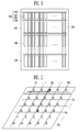
- FIG. 1 illustrates a plan view of an EL display device according to an exemplary embodiment of the present invention; and
- FIG. 2 illustrates a general diagram used to describe an exemplary method for detecting a failure of the EL display device illustrated in FIG. 1.
-
Korean Patent Application No. 10-2005-0127229, filed on December 21, 2005 - The present invention will now be described more fully hereinafter with reference to the accompanying drawings, in which exemplary embodiments of the invention are illustrated. The invention may, however, be embodied in different forms and should not be construed as limited to the embodiments set forth herein. In the figures, the dimensions of elements, layers, and regions may be exaggerated for clarity of illustration. It will also be understood that when an element or layer is referred to as being "on" another layer or substrate, it can be directly on the other layer or substrate, or intervening layers may also be present. Further, it will be understood that when an element is referred to as being "under" another element, it can be directly under, or one or more intervening elements may also be present. In addition, it will also be understood that when an element is referred to as being "between" two elements, it can be the only element between the two elements, or one or more intervening elements may also be present. Like reference numerals refer to like elements throughout.
- An exemplary embodiment of an electroluminescent (EL) display device according to the present invention is more fully described below with reference to FIG. 1. As illustrated in FIG. 1, an EL display device according to an embodiment of the present invention may include a
substrate 110, a plurality ofanode electrodes 120, a plurality ofcathode electrodes 150, a plurality oflight emitting layers 140, a plurality of cathode separators 130, and a testing array 200. The display includes display pixels and a test pixels. Hereinafter, a display pixel is a pixel that embodies a display triggered by an electric signal of a driver integrated circuit (IC). The testing array 200 incorporates test pixels, which are pixels for testing or detecting defects of the display pixel. The plurality ofanode electrodes 120 may be vertically arranged on thesubstrate 110 at predetermined intervals, and eachanode electrode 120 may be electrically connected to a driver integrated circuit (IC) through a data line. The plurality ofanode electrodes 120 may have a length sufficient to position thereon the plurality ofcathode electrodes 150, the plurality of cathode separators 130, and the testing array 200. The plurality ofanode electrodes 120 may be made of any known material in the art, e.g., indium tin oxide (ITO), indium zinc oxide (IZO), tin oxide (SnO2), and zinc oxide (ZnO). - The plurality of
cathode electrodes 150 may be arranged perpendicularly to the plurality ofanode electrodes 120, thereby forming a grid on thesubstrate 110. Eachcathode electrode 150 may be connected to a driver IC through a scan line and may be made of, e.g., lithium, magnesium, aluminum, aluminum-lithium, calcium, magnesium-indium, and magnesium-silver. - Each
light emitting layer 140 may be formed between theanode electrode 120 and thecathode electrode 150, such that thelight emitting layer 140 may be disposed at an intersection therebetween. Thelight emitting layer 140 may include an emission layer and additional functional layers, such as an electron injection layer, an electron transport layer, a hole injection layer, and a hole transport layer. Thelight emitting layer 140 may be formed of any light emitting material known in the art, e.g., phosphorescent material, fluorescent material, and so forth. For example, thelight emitting layer 140 may be made of an organic material to form an organic light-emitting layer.The plurality of cathode separators 130 may be positioned on thesubstrate 110 parallel to thecathode electrodes 150 to facilitate formation of the plurality ofcathode electrodes 150. In particular, each cathode separator 130 may be positioned between twoadjacent cathode electrodes 150 and perpendicularly to the plurality ofanode electrodes 120. - The testing array 200 may be constructed to facilitate testing of the EL display device, and the testing array 200 may be positioned on the
substrate 110 in parallel to thecathode electrodes 150. In particular, the testing array 200 may be positioned at an outer edge of thesubstrate 110, as illustrated in FIG. 1, such that it may be peripheral to anouter-most cathode electrode 150 and may intersect perpendicularly with the plurality ofanode electrodes 120. The testing array 200 may include atesting line 160, a testing emission layer 145, and atesting separator layer 125. The testing array 200 may be in communication with the plurality ofanode electrodes 120. - The
testing line 160 of the testing array 200 may be an electrode positioned in parallel to the plurality ofcathode electrodes 150. For example, thetesting line 160 may be positioned at an outermost position on thesubstrate 110 relative to the plurality ofcathode electrodes 150. It should be noted, however, that a distance between thetesting line 160 and anoutermost cathode electrode 150 may be smaller than a distance between any twocathode electrodes 150. Thetesting line 160 may be connected to a scan line; however, it may not receive signals from the driver IC. - Additionally, the
testing line 160 may have a smaller size as compared to any of thecathode electrodes 150. In particular, e.g., a width, i.e., a distance as measured in a direction parallel to theanode electrodes 120, of thetesting line 160 may be smaller as compared to a width of any of thecathode electrodes 150. For example, the plurality ofanode electrodes 120 may protrude a predetermined distance beyond the outermost cathode separator 130, such that thetesting line 160 may overlap with the protrudedanode electrode 120 without making significant changes in the EL display device layout. - The testing emission layer 145 of the testing array 200 may be made of the same material as the
light emitting layer 140, and the testing emission layer 145 may be disposed at each intersection of thetesting line 160 with each of the plurality ofanode electrodes 120. A size of the emission layer 145 disposed at the intersection between thetesting line 160 and theanode electrodes 120 may be smaller than a size of any of thelight emitting layers 140 disposed at any of the intersections between theanode electrodes 120 and thecathode electrodes 150. - The
testing separator layer 125 of the testing array 200 may be formed of the same material as the plurality of cathode separators 130, and it may be positioned parallel thereto. In particular, thetesting separator layer 125 may be positioned at an outermost position of thesubstrate 110 relative to thetesting line 160. - A single display emission cell consists of a display pixel comprising an
anode electrode 120, anorganic emission layer 140, and acathode electrode 150 formed on asubstrate 110. A test pixel extends ananode line 140 of a display pixel, and includes thetesting line 160 and the testing organic emission layer 145. In order to minimize an occupied area of the test pixel, it is preferred that a test pixel is smaller than a display pixel. In a structure of a typical light emitting display, a space remains at a peripheral portion of an outermost separator 130. Ananode electrode 120 protrudes into the space by a predetermined distance. By using this arrangement, the test pixel can be formed without changing the layout significantly. - When the EL display device according to an embodiment of the present invention is controlled by a passive-type driver, a driver IC may be electrically connected to a source/drain or gate electrode to transfer data signals and scan signals to each
anode electrode 120 andcathode electrode 150, respectively. - An exemplary method for detecting malfunctioning of the EL display device according to the invention will be described with respect to FIGS. 1-2. It should be noted, however, that the same elements are included in the embodiment illustrated in FIGS. 1-2. Accordingly, details and descriptions that may be found in both embodiments illustrated in FIGS. 1-2 will not be repeated herein.
- In this respect, it should further be noted that the data lines of the
anode electrodes 120 and the scan lines of thecathode electrodes 150 may be referred hereinafter as M data lines and N scan lines, respectively. Accordingly, the plurality of intersections therebetween may be referred to hereinafter as MxN pixels, and the testing array 200 may be referred to hereinafter as Mx1 test pixel array. - As illustrated in FIG. 2, in order to test the malfunctioning of the EL display device, the
testing line 160 may be grounded, and a direct current (DC) voltage may be inversely and sequentially applied to each scan line, i.e., q-th scan line, wherein (1≤q≤N). Subsequently, the testing array 200 may be monitored to determine a malfunction. In particular, emission of light from a p-th pixel, i.e., p-th position in the Mx1 array, wherein (1≤p≤M), in the testing array 200 may indicate malfunctioning of a pxq pixel in the EL display device. Lack of emitted light from the testing array 200 may indicate operational status of the EL display device. - Without intending to be bound by theory, it is believed that when DC voltage is applied inversely to a q-th scan line and the EL display device is operational, i.e., the EL device does not include any malfunctioning pixels in its q-th line, no electric current may be transferred and, therefore, no visual indicators, e.g., light, may be observed. Alternatively, when the EL display device is malfunctioning, i.e., the EL device may include points and/or pixels in its q-th line that are shorted, electric current may be transferred through the shorted pixel, e.g., pxq pixel, to the
testing line 160 and, thereby, trigger light emission from a p-th position in thetesting line 160, i.e. p-th pixel in the testing array 200. - Exemplary embodiments of the present invention have been disclosed herein, and although specific terms are employed, they are used and are to be interpreted in a generic and descriptive sense only and not for purpose of limitation.
-
- 110
- substrate
- 120
- anode electrode
- 125
- testing separator layer
- 130
- cathode separator
- 140
- light emitting layer
- 145
- testing emission layer
- 150
- cathode electrode
- 160
- testing line
- 200
- testing array
Claims (13)
- An electroluminescent display device, comprising:M anode electrodes (120), M being a positive integer;N cathode electrodes (150) intersecting the M anode electrodes (120) at right angles, N being a positive integer;a light emitting layer (140) disposed at each intersection of the M anode electrodes (120) and N cathode electrodes (150);a testing line (160) positioned at a peripheral position with respect to an outer-most cathode electrode of the N cathode electrodes (150), the testing line (160) being in communication with the M anode electrodes (120); anda testing emission layer (145) disposed between the testing line (160) and each of the M anode electrodes (120).
- The electroluminescent display device as claimed in claim 1, wherein each anode electrode (120) is connected to a respective data line and each cathode electrode (150) is connected to a respective scan line.
- The electroluminescent display device as claimed in claim 1 or 2, wherein a distance between the testing line (160) and the outermost cathode electrode is smaller than a distance between any two cathode electrodes (150).
- The electroluminescent display device according to at least one of the previous claims, wherein a size of the testing emission layer (145) is smaller than a size of the light emitting layer (140).
- The electroluminescent display device according to at least one of the previous claims, wherein the testing line (160) is parallel to the N cathode electrodes (150).
- The electroluminescent display device as claimed in claim 1, wherein the light emitting layer (140) is an organic light emitting layer.
- The electroluminescent display device according to at least one of the previous claims, wherein the testing emission layer (145) is an organic testing emission layer.
- The electroluminescent display according to at least one of the previous claims, wherein the plurality of anode electrodes (120) protrudes beyond the outermost cathode separator (130), such that the testing line (160) overlaps with the protruded anode electrode (120).
- The electroluminescent display according to at least one of the previous claims, wherein said testing array (200) incorporates a plurality of test pixels.
- The electroluminescent display according to claim 9, wherein the test pixels are arranged in a space at a peripheral portion of an outermost separator (130), into which an anode electrode (120) protrudes.
- A method for detecting a failure of an electroluminescent display device including a light emitting layer (140) formed at intersections of first M electrode lines and second N electrode lines, a testing line (160) for testing an element formed at outer sides of the second electrode lines parallel with the second electrode lines, and a testing emission layer (145) formed at an intersection of the testing line (160) and a first electrode line extending in a formation direction of the testing line, the method comprising:grounding the testing line (160) for testing the element;applying a direct current voltage to a q (1≤q≤N) line among the second electrode lines opposite to an applied direction of an electric current for driving the electroluminescent display device; anddetecting whether a (p×q)-th pixel is shorted by discriminating an emission of a p (1≤p≤M)-th testing pixel.
- The method as claimed in claim 11, wherein applying a direct current comprises separately applying an electric current to the second electrodes.
- The method as claimed in claim 11, wherein the electroluminescent display device is an organic light emitting display device.
Applications Claiming Priority (1)
| Application Number | Priority Date | Filing Date | Title |
|---|---|---|---|
| KR1020050127229A KR100719714B1 (en) | 2005-12-21 | 2005-12-21 | Organic light emitting display device and defect inspection method |
Publications (1)
| Publication Number | Publication Date |
|---|---|
| EP1801776A1 true EP1801776A1 (en) | 2007-06-27 |
Family
ID=37875968
Family Applications (1)
| Application Number | Title | Priority Date | Filing Date |
|---|---|---|---|
| EP06126756A Ceased EP1801776A1 (en) | 2005-12-21 | 2006-12-21 | Electroluminescent display device and method for detecting failure of the same |
Country Status (5)
| Country | Link |
|---|---|
| US (1) | US20070138956A1 (en) |
| EP (1) | EP1801776A1 (en) |
| JP (1) | JP2007173205A (en) |
| KR (1) | KR100719714B1 (en) |
| CN (1) | CN100544019C (en) |
Cited By (2)
| Publication number | Priority date | Publication date | Assignee | Title |
|---|---|---|---|---|
| EP2510513A4 (en) * | 2009-12-09 | 2013-05-22 | Luminator Holding Lp | SYSTEM AND METHOD FOR MONITORING A SIGNALING SYSTEM OF A TRANSIT VEHICLE |
| US9852670B2 (en) | 2010-02-25 | 2017-12-26 | Luminator Holding Lp | System and method for wireless control of signs |
Families Citing this family (8)
| Publication number | Priority date | Publication date | Assignee | Title |
|---|---|---|---|---|
| KR101365898B1 (en) | 2007-05-16 | 2014-02-24 | 엘지디스플레이 주식회사 | Organic light emitting device |
| KR102047002B1 (en) * | 2013-05-31 | 2019-11-21 | 삼성디스플레이 주식회사 | Organic light emitting display apparatus and method for repair thereof |
| CN106683605A (en) * | 2017-03-31 | 2017-05-17 | 京东方科技集团股份有限公司 | Failure pixel detection circuit and method and display device |
| CN109765736A (en) * | 2017-11-09 | 2019-05-17 | 瀚宇彩晶股份有限公司 | display panel |
| US11138931B2 (en) * | 2018-03-30 | 2021-10-05 | Sharp Kabushiki Kaisha | Display device and manufacturing method therefor |
| CN109490933B (en) * | 2018-10-22 | 2020-05-01 | 京东方科技集团股份有限公司 | Flat panel detector, detection method and X-ray detection device |
| KR102665221B1 (en) * | 2018-12-17 | 2024-05-09 | 엘지디스플레이 주식회사 | Organic light emitting diode display and manufacturing method of the same |
| CN113990212A (en) * | 2020-07-27 | 2022-01-28 | 北京芯海视界三维科技有限公司 | Light-emitting module and display device |
Citations (5)
| Publication number | Priority date | Publication date | Assignee | Title |
|---|---|---|---|---|
| WO2004042413A1 (en) * | 2002-11-06 | 2004-05-21 | Koninklijke Philips Electronics N.V. | Inspecting method and apparatus for a led matrix display |
| EP1538588A2 (en) * | 2003-11-25 | 2005-06-08 | Tohoku Pioneer Corp. | Self-light-emitting display module and method for verifying defect state of the same |
| US20050258859A1 (en) * | 2004-05-21 | 2005-11-24 | Franky So | Determining leakage in matrix-structured electronic devices |
| JP2005338532A (en) | 2004-05-28 | 2005-12-08 | Tohoku Pioneer Corp | Active drive type light emitting display device and electronic device equipped with the display device |
| US20060181195A1 (en) * | 2005-02-14 | 2006-08-17 | Tohoku Pioneer Corporation | Light emitting display panel and method for inspecting the light emitting display panel |
Family Cites Families (13)
| Publication number | Priority date | Publication date | Assignee | Title |
|---|---|---|---|---|
| US4924177A (en) * | 1983-04-29 | 1990-05-08 | Mulz Robert H | Tester for solid state electronic components |
| CA2384592C (en) * | 2000-07-28 | 2009-05-19 | Nichia Corporation | Light element test method and device using the light element driving circuit |
| US6573660B2 (en) * | 2001-04-30 | 2003-06-03 | Intel Corporation | Driving emissive displays |
| KR100870615B1 (en) * | 2002-06-29 | 2008-11-25 | 오리온오엘이디 주식회사 | Organic EL panel and defect inspection method |
| JP2004205704A (en) * | 2002-12-24 | 2004-07-22 | Toshiba Matsushita Display Technology Co Ltd | Organic el display |
| JP2004342395A (en) * | 2003-05-14 | 2004-12-02 | Shoka Kagi Kofun Yugenkoshi | Organic light emitting diode display |
| KR100601368B1 (en) * | 2003-09-08 | 2006-07-13 | 삼성에스디아이 주식회사 | Evaluation means of characteristics of organic light emitting display device |
| JP2005274821A (en) * | 2004-03-24 | 2005-10-06 | Tohoku Pioneer Corp | Spontaneous light emission module, electronic equipment mounted with same module, and method for verifying defect state of same module |
| JP4239890B2 (en) * | 2004-04-26 | 2009-03-18 | セイコーエプソン株式会社 | Organic EL devices, electronic devices |
| JP4421990B2 (en) * | 2004-09-30 | 2010-02-24 | スガツネ工業株式会社 | Earth leakage detector |
| KR100726639B1 (en) * | 2004-10-21 | 2007-06-11 | 엘지전자 주식회사 | Organic electroluminescent display device, manufacturing method and inspection method thereof |
| KR100731741B1 (en) * | 2005-04-29 | 2007-06-22 | 삼성에스디아이 주식회사 | Organic light emitting device |
| JP2008039462A (en) * | 2006-08-02 | 2008-02-21 | Fujitsu Ltd | Display panel inspection apparatus and method |
-
2005
- 2005-12-21 KR KR1020050127229A patent/KR100719714B1/en not_active Expired - Fee Related
-
2006
- 2006-08-24 JP JP2006228202A patent/JP2007173205A/en active Pending
- 2006-12-21 US US11/642,581 patent/US20070138956A1/en not_active Abandoned
- 2006-12-21 CN CNB2006101705397A patent/CN100544019C/en active Active
- 2006-12-21 EP EP06126756A patent/EP1801776A1/en not_active Ceased
Patent Citations (5)
| Publication number | Priority date | Publication date | Assignee | Title |
|---|---|---|---|---|
| WO2004042413A1 (en) * | 2002-11-06 | 2004-05-21 | Koninklijke Philips Electronics N.V. | Inspecting method and apparatus for a led matrix display |
| EP1538588A2 (en) * | 2003-11-25 | 2005-06-08 | Tohoku Pioneer Corp. | Self-light-emitting display module and method for verifying defect state of the same |
| US20050258859A1 (en) * | 2004-05-21 | 2005-11-24 | Franky So | Determining leakage in matrix-structured electronic devices |
| JP2005338532A (en) | 2004-05-28 | 2005-12-08 | Tohoku Pioneer Corp | Active drive type light emitting display device and electronic device equipped with the display device |
| US20060181195A1 (en) * | 2005-02-14 | 2006-08-17 | Tohoku Pioneer Corporation | Light emitting display panel and method for inspecting the light emitting display panel |
Cited By (12)
| Publication number | Priority date | Publication date | Assignee | Title |
|---|---|---|---|---|
| EP2510513A4 (en) * | 2009-12-09 | 2013-05-22 | Luminator Holding Lp | SYSTEM AND METHOD FOR MONITORING A SIGNALING SYSTEM OF A TRANSIT VEHICLE |
| US9530336B2 (en) | 2009-12-09 | 2016-12-27 | Luminator Holding Lp | System and method for monitoring a signage system of a transit vehicle |
| US9990876B2 (en) | 2009-12-09 | 2018-06-05 | Luminator Holding Lp | System and method for monitoring a signage system of a transit vehicle |
| US10304367B2 (en) | 2009-12-09 | 2019-05-28 | Luminator Holding Lp | System and method for monitoring a signage system of a transit vehicle |
| US10559240B2 (en) | 2009-12-09 | 2020-02-11 | Luminator Holding Lp | System and method for monitoring a signage system of a transit vehicle |
| US10726757B2 (en) | 2009-12-09 | 2020-07-28 | Luminator Holding Lp | System and method for monitoring a signage system of a transit vehicle |
| US11100827B2 (en) | 2009-12-09 | 2021-08-24 | Luminator Holding Lp | System and method for monitoring a signage system of a transit vehicle |
| US11626046B2 (en) | 2009-12-09 | 2023-04-11 | Laminator Holding LP | System and method for monitoring a signage system of a transit vehicle |
| US9852670B2 (en) | 2010-02-25 | 2017-12-26 | Luminator Holding Lp | System and method for wireless control of signs |
| US10607517B2 (en) | 2010-02-25 | 2020-03-31 | Luminator Holding Lp | System and method for wireless control of signs |
| US11100823B2 (en) | 2010-02-25 | 2021-08-24 | Luminator Holding Lp | System and method for wireless control of signs |
| US11776437B2 (en) | 2010-02-25 | 2023-10-03 | Luminator Holding Lp | System and method for wireless control of signs |
Also Published As
| Publication number | Publication date |
|---|---|
| KR100719714B1 (en) | 2007-05-17 |
| US20070138956A1 (en) | 2007-06-21 |
| JP2007173205A (en) | 2007-07-05 |
| CN1988170A (en) | 2007-06-27 |
| CN100544019C (en) | 2009-09-23 |
Similar Documents
| Publication | Publication Date | Title |
|---|---|---|
| US10861361B2 (en) | Display device | |
| US11706941B2 (en) | Organic light emitting display device | |
| US10854133B2 (en) | Micro LED display panel | |
| US20210343606A1 (en) | Display device | |
| KR102402084B1 (en) | Display device | |
| US10541281B2 (en) | In-cell touch organic light-emitting display device | |
| US11751464B2 (en) | Display substrate and display device | |
| KR102217455B1 (en) | Display device | |
| CN111106151B (en) | Electronic device with a detachable cover | |
| US8338832B2 (en) | Organic light emitting display device | |
| CN110673766A (en) | A touch display panel and its detection method | |
| US6882103B2 (en) | Panel of organic electroluminescence device and method for manufacturing the same | |
| US10411076B2 (en) | EL display device | |
| US8674954B2 (en) | Organic light emitting diode display and method of manufacturing the same | |
| CN101320736A (en) | Organic light-emitting display device and its motherboard | |
| US20220254830A1 (en) | Display device | |
| US20140354700A1 (en) | Repairable organic light-emitting display apparatus and method of repairing the same | |
| US20070138956A1 (en) | Electroluminescent display device and method for detecting failure of the same | |
| KR20180004881A (en) | Printed circuit board package and display device including the same | |
| KR100434276B1 (en) | organic electroluminescence device | |
| US20230397460A1 (en) | Display panel and display apparatus | |
| CN103187017B (en) | For the ageing system of display device and utilize the aging method of this ageing system | |
| CN115207072B (en) | Display panel and manufacturing method thereof, and display device | |
| CN113485586A (en) | Touch control display panel | |
| US12242690B2 (en) | Panel, motherboard, and display device |
Legal Events
| Date | Code | Title | Description |
|---|---|---|---|
| PUAI | Public reference made under article 153(3) epc to a published international application that has entered the european phase |
Free format text: ORIGINAL CODE: 0009012 |
|
| 17P | Request for examination filed |
Effective date: 20061221 |
|
| AK | Designated contracting states |
Kind code of ref document: A1 Designated state(s): AT BE BG CH CY CZ DE DK EE ES FI FR GB GR HU IE IS IT LI LT LU LV MC NL PL PT RO SE SI SK TR |
|
| AX | Request for extension of the european patent |
Extension state: AL BA HR MK YU |
|
| 17Q | First examination report despatched |
Effective date: 20080124 |
|
| AKX | Designation fees paid |
Designated state(s): DE FR GB |
|
| RAP1 | Party data changed (applicant data changed or rights of an application transferred) |
Owner name: SAMSUNG MOBILE DISPLAY CO., LTD. |
|
| STAA | Information on the status of an ep patent application or granted ep patent |
Free format text: STATUS: THE APPLICATION HAS BEEN REFUSED |
|
| 18R | Application refused |
Effective date: 20090427 |