EP1801564B1 - Dispositif et procédé pour la fourniture de lumière aux canaux ou portions - Google Patents
Dispositif et procédé pour la fourniture de lumière aux canaux ou portions Download PDFInfo
- Publication number
- EP1801564B1 EP1801564B1 EP06126528.6A EP06126528A EP1801564B1 EP 1801564 B1 EP1801564 B1 EP 1801564B1 EP 06126528 A EP06126528 A EP 06126528A EP 1801564 B1 EP1801564 B1 EP 1801564B1
- Authority
- EP
- European Patent Office
- Prior art keywords
- light
- channel
- component
- angle
- longitudinal direction
- Prior art date
- Legal status (The legal status is an assumption and is not a legal conclusion. Google has not performed a legal analysis and makes no representation as to the accuracy of the status listed.)
- Expired - Fee Related
Links
Images


Classifications
-
- G—PHYSICS
- G01—MEASURING; TESTING
- G01N—INVESTIGATING OR ANALYSING MATERIALS BY DETERMINING THEIR CHEMICAL OR PHYSICAL PROPERTIES
- G01N21/00—Investigating or analysing materials by the use of optical means, i.e. using sub-millimetre waves, infrared, visible or ultraviolet light
- G01N21/01—Arrangements or apparatus for facilitating the optical investigation
- G01N21/03—Cuvette constructions
- G01N21/05—Flow-through cuvettes
-
- B—PERFORMING OPERATIONS; TRANSPORTING
- B01—PHYSICAL OR CHEMICAL PROCESSES OR APPARATUS IN GENERAL
- B01L—CHEMICAL OR PHYSICAL LABORATORY APPARATUS FOR GENERAL USE
- B01L3/00—Containers or dishes for laboratory use, e.g. laboratory glassware; Droppers
- B01L3/50—Containers for the purpose of retaining a material to be analysed, e.g. test tubes
- B01L3/502—Containers for the purpose of retaining a material to be analysed, e.g. test tubes with fluid transport, e.g. in multi-compartment structures
- B01L3/5027—Containers for the purpose of retaining a material to be analysed, e.g. test tubes with fluid transport, e.g. in multi-compartment structures by integrated microfluidic structures, i.e. dimensions of channels and chambers are such that surface tension forces are important, e.g. lab-on-a-chip
- B01L3/502715—Containers for the purpose of retaining a material to be analysed, e.g. test tubes with fluid transport, e.g. in multi-compartment structures by integrated microfluidic structures, i.e. dimensions of channels and chambers are such that surface tension forces are important, e.g. lab-on-a-chip characterised by interfacing components, e.g. fluidic, electrical, optical or mechanical interfaces
-
- G—PHYSICS
- G01—MEASURING; TESTING
- G01N—INVESTIGATING OR ANALYSING MATERIALS BY DETERMINING THEIR CHEMICAL OR PHYSICAL PROPERTIES
- G01N21/00—Investigating or analysing materials by the use of optical means, i.e. using sub-millimetre waves, infrared, visible or ultraviolet light
- G01N21/01—Arrangements or apparatus for facilitating the optical investigation
- G01N21/03—Cuvette constructions
- G01N21/0303—Optical path conditioning in cuvettes, e.g. windows; adapted optical elements or systems; path modifying or adjustment
-
- B—PERFORMING OPERATIONS; TRANSPORTING
- B01—PHYSICAL OR CHEMICAL PROCESSES OR APPARATUS IN GENERAL
- B01L—CHEMICAL OR PHYSICAL LABORATORY APPARATUS FOR GENERAL USE
- B01L2300/00—Additional constructional details
- B01L2300/06—Auxiliary integrated devices, integrated components
- B01L2300/0627—Sensor or part of a sensor is integrated
- B01L2300/0654—Lenses; Optical fibres
-
- B—PERFORMING OPERATIONS; TRANSPORTING
- B01—PHYSICAL OR CHEMICAL PROCESSES OR APPARATUS IN GENERAL
- B01L—CHEMICAL OR PHYSICAL LABORATORY APPARATUS FOR GENERAL USE
- B01L2300/00—Additional constructional details
- B01L2300/08—Geometry, shape and general structure
- B01L2300/0809—Geometry, shape and general structure rectangular shaped
- B01L2300/0816—Cards, e.g. flat sample carriers usually with flow in two horizontal directions
-
- B—PERFORMING OPERATIONS; TRANSPORTING
- B01—PHYSICAL OR CHEMICAL PROCESSES OR APPARATUS IN GENERAL
- B01L—CHEMICAL OR PHYSICAL LABORATORY APPARATUS FOR GENERAL USE
- B01L2300/00—Additional constructional details
- B01L2300/16—Surface properties and coatings
- B01L2300/168—Specific optical properties, e.g. reflective coatings
-
- G—PHYSICS
- G01—MEASURING; TESTING
- G01N—INVESTIGATING OR ANALYSING MATERIALS BY DETERMINING THEIR CHEMICAL OR PHYSICAL PROPERTIES
- G01N21/00—Investigating or analysing materials by the use of optical means, i.e. using sub-millimetre waves, infrared, visible or ultraviolet light
- G01N21/01—Arrangements or apparatus for facilitating the optical investigation
- G01N21/03—Cuvette constructions
- G01N2021/0346—Capillary cells; Microcells
-
- G—PHYSICS
- G01—MEASURING; TESTING
- G01N—INVESTIGATING OR ANALYSING MATERIALS BY DETERMINING THEIR CHEMICAL OR PHYSICAL PROPERTIES
- G01N21/00—Investigating or analysing materials by the use of optical means, i.e. using sub-millimetre waves, infrared, visible or ultraviolet light
- G01N21/62—Systems in which the material investigated is excited whereby it emits light or causes a change in wavelength of the incident light
- G01N21/63—Systems in which the material investigated is excited whereby it emits light or causes a change in wavelength of the incident light optically excited
- G01N21/64—Fluorescence; Phosphorescence
-
- G—PHYSICS
- G01—MEASURING; TESTING
- G01N—INVESTIGATING OR ANALYSING MATERIALS BY DETERMINING THEIR CHEMICAL OR PHYSICAL PROPERTIES
- G01N21/00—Investigating or analysing materials by the use of optical means, i.e. using sub-millimetre waves, infrared, visible or ultraviolet light
- G01N21/62—Systems in which the material investigated is excited whereby it emits light or causes a change in wavelength of the incident light
- G01N21/63—Systems in which the material investigated is excited whereby it emits light or causes a change in wavelength of the incident light optically excited
- G01N21/65—Raman scattering
Definitions
- the present invention relates to providing light to channels or portions of channels.
- U.S. Patent No. 6,580,507 describes a multiple-longitudinal flow cell channel system in which an array detector is positioned to monitor radiation from at least two of multiple flow cell channels, at separate groupings of pixels on the detector.
- WO00/62050 A1 discloses a detection apparatus comprising a separation channel for measuring the velocity of items within said channel.
- the separation channel may comprise an anti-resonant reflecting optical waveguide (ARROW).
- ARROW anti-resonant reflecting optical waveguide
- US 6,490,034 B1 discloses a measuring cell for determining an optical absorption of a sample fluid or for use as a reactor for carrying out an optically detectable chemical reaction.
- the measuring cell uses etching techniques to provide silicon structures that may be used to mount reflectors for propagating light through the cell.
- K Singh et al "Analysis of cellular structure by light scattering measurements in a new cytometer design based on a liquid-core waveguide", IEE Proc.-Nanobiotechnol. 151(1) (February 2004) 10-16 describes the results of applying a microfluidic optical cytometer to generate and observe the light scattered from biological cells over a wide range of angles.
- the cytometer incorporates a waveguide that increases the intensity of the scattered light to the extent that an inexpensive digital camera can be used to detect the light over a large solid angle.
- the cytometer includes a leaky waveguide consisting of a microfluidic channel fabricated on a glass substrate with a glass superstrate.
- light refers herein to electromagnetic radiation of any wavelength or frequency; unless otherwise indicated, a specific value for light wavelength or frequency is that of light propagating through vacuum.
- photon refers herein to a quantum of light
- photon energy refers herein to the energy of a photon.
- the various exemplary implementations described below address problems that arise in propagating light in certain contexts.
- the implementations address problems that arise in efficiently and effectively illuminating objects, especially in situations in which photons emanate from objects in response to propagating light and in situations in which many objects are far apart from each other and all of them should be illuminated, such as for large area excitation.
- the emanating photons can be sensed.
- optical waveguides can be used, but usually the fluid or other substance that contains the analyte cannot itself be used as an optical waveguide, because its refractive index is lower than the index of surrounding material. Therefore, a conventional optical waveguide typically provides only weak interaction with target molecules, through evanescent waves along the periphery of the waveguide.
- microfabrication Some of the photosensing implementations described herein employ structures with one or more dimensions smaller than 1 mm, and various techniques have been proposed for producing such structures. In particular, some techniques for producing such structures are referred to as "microfabrication.” Examples of microfabrication include various techniques for depositing materials such as growth of epitaxial material, sputter deposition, evaporation techniques, plating techniques, spin coating, printing, and other such techniques; techniques for patterning materials, such as etching or otherwise removing exposed regions of thin films through a photolithographically patterned resist layer or other patterned layer; techniques for polishing, planarizing, or otherwise modifying exposed surfaces of materials; and so forth.
- Fig. 1 shows schematically some components of analyzer 10 on support structure 12, a fluidic structure.
- support structure 12 defines serpentine channel 14 through which an object 16 can travel, carried by a fluid or other appropriate substance.
- Object 16 can be a droplet or small volume of fluid that includes an analyte.
- a droplet or small volume of fluid may include atoms, molecules, or other particles that emit light spontaneously or in response to excitation; a particle could be a "fluorescent component" of a droplet, fluorescing in response to excitation.
- a droplet may include particles that absorb light incident on the droplet, so that the droplet does not reflect or otherwise scatter the absorbed light; in this case, a particle could be an "absorbent component" of a droplet.
- a droplet may include particles that scatter light incident on the droplet in a way that depends on photon energy, so that the droplet scatters the incident light correspondingly; in this case, a particle could be an "scattering component" of a droplet.
- An analyte i.e. a chemical species being investigated
- a droplet can act as a fluorescent, absorbent, or scattering component.
- Object 16 enters channel 14 carried by a primary fluid illustrated by arrow 20, and can enter from a supply reservoir (not shown) and a sample well (not shown), with its entry into the primary fluid controlled by metering electrodes 22.
- metering electrodes 22 Rather than electrical metering, as with electrodes 22, pressure metering or other techniques could be used.
- Other possible techniques that could be implemented to provide a droplet or other small object to channel 14 could employ capillary forces or electro-osmotic flow pumps..
- Analyzer 10 could be implemented with any appropriate number of channels similar to channel 14, and with each channel receiving analyte samples from a respective sample well. Each of the channels could have a different combination of components suitable to a specific type of analysis.
- the channels could be formed by subdividing a broad channel into several parallel channels.
- Additional fluid to carry object 16 may enter as shown by arrow 24.
- the path followed by the fluid in channel 14 can be controlled through a number of devices.
- the fluid, together with object 16 if appropriately positioned, can be purged at two outlets as illustrated by arrows 26 and 28 through toggling of valves 30 and 32, respectively, each of which is at a bifurcation junction.
- Other types of gates could be used; charged particles could be deflected by Coulomb force, and polarizable particles could be deflected by dielectrophoretic force.
- Fluid can also be purged at a final outlet from channel 14, illustrated by arrow 34.
- the flow of the fluid can be maintained by conventional propulsion components such as electro-osmotic pumps 40 or some suitable hydraulic pressure pump appropriately positioned along the length of channel 14.
- propulsion components such as electro-osmotic pumps 40 or some suitable hydraulic pressure pump appropriately positioned along the length of channel 14.
- Other propulsion components could be used, including, for example, gas pressure pumps, positive displacement pumps, micro-peristaltic pumps, electro-kinetic pumps, piezo pumps, and thermal mode pumps.
- Propulsion components can also perform system flush and initial fluid loading functions, with pressure driven techniques. Appropriate circuitry can coordinate the various pumps and other components to work in a synchronized manner.
- Coulter counter 50 is an electrically based particle size detector.
- Mie scatter sensor 52 is an optical detector that relies on particle-induced scattering of light entering from the side of channel 14.
- Coulter counter 50 can be implemented to size particles in the 1-10 ⁇ m range within a continuous liquid stream.
- the Coulter counter technique should also work for other particle sizes as long as the inner diameter of channel 14 in the sensing region is not more than an order of magnitude larger than the particles being measured.
- the series of sensing components also includes optical (e.g. visible or infrared) absorption sensing component 54, first fluorescence sensing component 56, second fluorescence sensing component 58, and Raman scatter sensing component 60.
- Additional sensing components could include conventional optical or electrical trigger elements that provide a signal indicating when an analyte with properties meeting certain criteria moves past a position along channel 14.
- sensing components for electrical impedance spectroscopy (EIS) for electronic pathology rather than sensing differential resistance for bioparticle sizing.
- a series of sensing components as in Fig. 1 makes it possible to obtain spectral information about moving particles or other objects in order to achieve orthogonal characterization and reliable identification. Characterization is orthogonal if sensing components obtain information about orthogonal characteristics of a moving object, such as by photosensing different ranges of photon energies; sensing components could also be suitable for different intensity ranges. By choosing suitable materials, it is possible to obtain spectral information for the entire range from the deep ultraviolet to the far infrared or even for frequencies in the THz range.
- Analyzer 10 can be designed to perform multi-signal analysis for a specific application, whether high wavelength resolution or broadband detection is desired.
- the technique illustrated in Fig. 1 also takes advantage of the motion of object 16 with a geometry that enables long integration times without sacrificing throughput capacity.
- Highly sensitive optical characterization methods can be used, such as fluorescence spectroscopy (illustratively in more than one range of photon energies) and Raman spectroscopy.
- fluorescence spectroscopy illustrated in more than one range of photon energies
- Raman spectroscopy Raman spectroscopy
- Each of sensing components 54, 56, 58, and 60 includes a respective one of ICs 64, 66, 68, and 70.
- Each of these ICs includes a photosensor array, and the sensing component includes a set of cells of the photosensor array.
- the set of cells photosenses photons within a range of photon energies; the sets of cells in ICs 66 and 68 could photosense different ranges of photon energies in the visible to ultraviolet range, and, as noted above, the set of cells in IC 70 could photosense in the infrared.
- More than one IC could photosense fluorescing photons that are in the same energy range, but that result from excitation at different wavelengths such as from different LED or laser light sources.
- the set of cells for each of sensing components 54, 56, 58 and 60 includes a subset of cells, each of which photosenses in a respective subrange, and the subranges of at least two of the cells are different from each other.
- Sensing components 56, 58, and 60 can each be implemented with any suitable excitation or illumination technique to cause emanation of light from objects.
- An excitation component could provide electromagnetic wave excitation or a reagent.
- An illumination componentcould provide light, such as to cause emission or scattering of photons from illuminated objects.
- An illumination component can include one or more light.
- an anti-resonant waveguide has a core region surrounded by a cladding layer with a higher refractive index than the core region.
- the core region is a fluid that contains an analyte
- light can be guided within the fluid, permitting photonic interaction over an extended length of a channel such as channel 14.
- ICs 66, 68, and 70 are supported on spacers 72, providing a suitable gap between each IC and the respective portion of channel 14 to avoid interference with anti-resonant waveguiding.
- the interaction between light and target molecules is typically very weak.
- Techniques in which light propagates in a longitudinal direction can improve the interaction because of the extended length in which interaction occurs.
- such techniques are very suitable for multi-signal analysis because they are relatively unaffected by changes in wavelength or film thickness.
- fluidic channels with maximum transverse dimensions as great as a few millimeters can be used as anti-resonant waveguides.
- Suitable configurations can include an aerosol in a glass capillary tube or a liquid film between glass slides. The excitation could be any appropriate electromagnetic radiation.
- Background suppression of excitation light can be obtained using a wavelength filtering component as part of the wall of channel 14 or as an additional coating on top of a photosensor array.
- Fig. 2 shows schematically a cross section of analyzer 10 taken along the line 2-2 in Fig. 1 . Similar features would be found in first fluorescence sensing component 56 and, to an extent, in Raman scatter sensing component 60.
- portion 80 of channel 14 As object 16 travels through portion 80 of channel 14 in the downstream direction indicated by arrow 82, it receives light from an excitation component, illustratively light source 84 which could be a laser or an LED; in general, excitation radiation in any of various different energy ranges can be coupled into channel 14 to produce anti-resonant waveguiding.
- an excitation component illustratively light source 84 which could be a laser or an LED; in general, excitation radiation in any of various different energy ranges can be coupled into channel 14 to produce anti-resonant waveguiding.
- portion 80 can function as an anti-resonant waveguide in response to light from source 84, or in another way that provides enhanced light-target interaction.
- Other techniques that provide continuous excitation to a fluorescing molecule include tracking the molecule in motion with a scanning laser beam; using a linear array of LEDs to sustain particle excitation along its path; arranging a collimated beam along the particle path without waveguiding; and providing a Fabry-Perot-style cavity in which light passes through the medium containing the particle several times.
- Sensing components using anti-resonant waveguide modes are especially advantageous in combination with fluidic devices because the fluidic channels themselves can be used as anti-resonant waveguides in various configurations. Examples of configurations include an aerosol carrying analytes in a capillary, a liquid film carrying analytes within a channel or between glass slides, etc.
- an analyte within object 16 fluoresces, emitting light with a characteristic spectrum of photon energies.
- a portion 86 of the light is emitted toward assembly 87, which includes at least IC 68.
- Photons in portion 86 can therefore be photosensed by cells of a photosensor array on IC 68.
- Assembly 87 is positioned so that the photosensor array on IC 68 is close to and parallel to the path of object 16 through portion 80, to increase light collection efficiency.
- a photosensor array is "positioned along” or “along” a channel or a portion of a channel if the array is positioned near the channel or portion in such a way that one or more of its photosensors can photosense light emanating from the channel or portion.
- Assembly 87 is illustratively supported on spacers 72 to avoid disturbing anti-resonant waveguiding.
- Spacers 72 are positioned outside portion 80, and, as a result, air gap 88 below assembly 87 prevents disturbance of waveguiding.
- Any other appropriate structure could be provided that would prevent disturbance of waveguiding; examples include a gas or vacuum layer or possibly even a liquid layer or film with a low refractive index.
- the structure shown in Fig. 2 could also be used to implement Raman scatter sensing component 60.
- the output signal could indicate a set of intensity ratios of selected Raman lines and/or certain narrow intervals of a Raman spectrum rather than a complete Raman spectrum.
- a fluorescence sensing component could include a photosensor array in which cells photosense within a wide spectral range with rather low resolution, e.g. 400-700 nm with a moderate wavelength resolution of 2-5 nm.
- a Raman scatter sensing component could include a photosensor array in which cells photosense within a smaller spectral range close to the excitation wavelength but with greater resolution, e.g. 800-830 nm with a resolution of 0.2-0.5 nm or even higher resolution.
- Fig. 2 also illustrates support structure 12.
- Support layer 90 could be a light-transmissive glass or silicon substrate.
- Channel 14 can be defined in a micromolded layer 92 of polydimethylsiloxane (PDMS).
- PDMS polydimethylsiloxane
- Techniques for producing a patterned layer of PDMS include fabricating a template on glass from SU-8 polymer, and then depositing PDMS to form a patterned structure within the template. The template can then be removed.
- Over layer 92 is a plate 94, such as glass and therefore another example of a light-transmissive structure.
- channels could be microfabricated by patterning a layer of a polymer material such as SU-8 to produce high aspect ratio channel walls. Depending on the medium that carries analyte through channel 14, parameters of channel 14 can be modified for optimal results.
- the thicknesses of layers 90 and 94 can bear a desired relationship to the height of channel 14, depending on various constraints, including stability requirements, manufacturing convenience, and, as noted below, the need to accommodate a desired flow of fluid and objects through channel 14. Thicknesses of layers 90 and 94 are often greater than or approximately equal to the height of channel 14. Typical thicknesses range between approximately 100 ⁇ m and 2 mm. Channel height ranges from approximately 1 ⁇ m or less up to a few mm.
- a specific parameter of channel 14 that can have significant effects is adhesiveness of the channel wall.
- An anti-adhesive coating can be applied to prevent bioparticles and other analytes from sticking to the walls. Dip-coated polyethylene glycol (PEG) is a good choice for preventing adhesion of most biomaterials and can maintain capillary force on aqueous solutions. Other coatings may be viable options depending on sample properties, material interface chemistry, and operating conditions and regimes; for example, parylene C or vapor deposited tetraglyme might provide appropriate coatings.
- Anti-resonant waveguiding techniques can employ a channel with an inner diameter at least up to approximately 1.0 mm and possibly greater, in which case adhesion is not as great a problem and clogging is unlikely to occur; nevertheless, anti-adhesion measures may be advantageous.
- Fig. 2 also shows optical component 96 on the side of support layer 90 opposite PDMS layer 92.
- Optical component 96 provides an appropriate surface 98 through which light from source 84 can be coupled into the anti-resonant waveguide within portion 80 of channel 14.
- Support layer 90 and optical component 96 could instead be fabricated from a single layer of material.
- Fig. 3 is a schematic view of an implementation of assembly 87 in which IC 68 includes photosensor array 100 and also has spacers 72 attached to it.
- Photosensor array 100 is a two-dimensional array, with at least two rows of cells that include photosensors.
- photosensor array 100 can be provided with different coatings or can be otherwise structured so that their cells photosense different ranges or subranges of photon energies.
- the information obtained from a single IC can provide a detailed analysis of incident photons over a broad range of photon energies.
- Reference cells such as the cells in row 102, can be used to provide a spatially resolved real-time reference signal.
- Each cell in row 102 photosenses photons throughout a suitable range, characterized as ⁇ all , to produce a reference for a nearby cell in row 104.
- the cell in row 102 must be different from the cells in row 104. For example, it could have a different sensing area or it could have a gray filter coating different than a coating over the paired cell in row 104.
- Each cell in row 104 photosenses a respective subrange between ⁇ min and ⁇ max , with illustrative cell 106 photosensing a subrange centered around ⁇ p .
- IC 68 also includes array circuitry as well as peripheral circuitry 110 which perform various functions relating to readout of photosensed information from array 100.
- IC 68 provides a compact photosensor array that can be used for various functions within a system such as analyzer 10.
- the compactness of IC 68 also allows for an interactive detection scheme. Subsequent or adjacent ICs within analyzer 10 may exchange information or trigger events. The combination of analysis results from several ICs within analyzer 10 may help to obtain orthogonal information and ultimately enable reliable identification of object 16.
- one useful criterion is the proportion of light intensity that occurs in fluid.
- a total light intensity of longitudinally propagating light can be integrated over the entire cross section, including the material around the boundary, and a partial light intensity can be integrated solely over the area within the boundary, i.e. the area that can contain fluid.
- the ratio of the partial light intensity to the total light intensity is a proportion that can be expressed as a percentage.
- a proportion N of light intensity "occurs" in fluid if the ratio of partial to total light intensity obtained in this manner is N.
- Fig. 4 shows a cross section of channel 14 along the line 4-4 in Fig. 2 .
- Assembly 87 is separated from layer 94 by gap 88, due to spacers 72.
- Layers 90 and 94 provide the upper and lower boundaries of channel 14, and the lateral boundaries are provided by walls 120 and 122 formed in layer 92 ( Fig. 2 ).
- the specific relation of W to H in Fig. 4 is merely illustrative; various W/H ratios can be used in anti-resonant waveguides. As noted above, however, the height H must be sufficiently large to accommodate the desired flow or throughput of fluid and objects through channel 14 and to avoid blockage, such as due to adhesion. Also, the ratios Z 1 /H and Z 2 /H can be adjusted.
- Fig. 5 illustrates exemplary distributions of light intensity that might occur across channel 14 along the z-direction.
- Curve 126 shows a Gaussian distribution resulting from excitation of a first anti-resonant waveguide mode.
- Curve 128 shows a nearly uniform distribution within the channel resulting from excitation of many modes.
- the indices of refraction of layers 90 and 94 and of walls 120 and 122 are all at least slightly greater than that of the fluid contained in channel 14, an arrangement that permits generation of an anti-resonant wave within channel 14 if illuminated at an appropriate angle of incidence.
- the indices of refraction of layers 90 and 94 and of walls 120 and 122 might be between 1.4 and 1.8, while the index of refraction of the fluid might be between 1.2 and 1.4.
- semiconductor materials might be used, such as silicon, gallium arsenide, gallium nitride, or zinc oxide; silicon, for example, might be suitable for very small channels and infrared illumination.
- the Eigensolutions or optical modes for the waveguide structure illustrated in Fig. 4 can be obtained by calculations, enabling computation of indices of refraction and modal confinement factors of the modes. Each such mode can be excited or coupled by light entering the waveguide at a specific angle of incidence corresponding to the effective refractive index.
- the confinement factor of a mode corresponds to the fraction of the light intensity confined within the boundary of the waveguide, i.e. within channel 14.
- a mode can be selected with a desired confinement factor, up to and possibly greater than 90%.
- such a mode must have an effective refractive index close to, and typically slightly smaller than, the refractive index of the core material, illustratively the fluid in channel 14.
- the effective refractive indices of these modes approach the refractive index of the core.
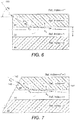
- Fig. 6 illustrates schematically how light provided to an end facet of channel 14 could result in longitudinal propagation of light in an anti-resonant waveguide mode.
- the refractive index of the fluid in channel 14 is n
- the refractive indices of layers 90 and 94 are both n'
- An optimum angle of incidence ⁇ " of representative incident light ray 130 can be derived.
- the implementation in Fig. 7 minimizes losses caused by large angles of incidence like that of ray 130 in Fig. 6 .
- Reflections at surface 140 are minimized if incident light ray 142 enters at or near a normal to surface 140.
- ray 142 can enter surface 140 and still strike the interface 144 between layer 94 and the fluid in channel 14 at an angle suitable to couple to an anti-resonant waveguide mode.
- Fig. 8 illustrates a problem that arises where it is impractical to illuminate channel 14 through a facet surface as in Figs. 6 and 7 .
- the only portion of channel 14 capable of functioning as an anti-resonant waveguide is the portion between inlet port 150 and outlet port 152.
- the implementation of Fig. 8 includes end components 160 and 162, which can include the same material as layer 92 or other suitable material such as Gelpak® film, PDMS, SU-8 or other photoresist material, glass, or quartz. End components 160 and 162 interfere with illumination through end facet surfaces, which would also be true if they were instead connected as entry and exit ports.
- layer 94 and other material bounding anti-resonant waveguides portions is light-transmissive, it is possible to illuminate channel 14 by providing light to the upper surface 164 of layer 94. As illustrated, for light ray 170, the angle of incidence is inappropriate for coupling to an anti-resonant waveguide mode of channel 14. Instead, most of the light provided through ray 170 is transmitted through layer 94, through the fluid in channel 14, and through layer 90, exiting as ray 172.
- Fig. 9 illustrates an alternative implementation in which channel 14 includes two portions, with portion 180 capable of containing fluid and with portion 182 containing air. Portions 180 and 182 are separated by bounding component 184, which can include the same or similar materials to those of end components 160 and 162, but can be as thin as possible for optical purposes while being sufficiently thick to be manufacturable and to preserve a fluidic barrier between portions 180 and 182. As a result, portion 182 is a projection of portion 180 beyond bounding component 184.
- Bounding component 184 can alternatively have a convex surface disposed toward portion 182, so that light entering from portion 182 is focused or, in the case of divergent light such as from a poorly collimated LED source, becomes more collimated.
- incident light ray 190 As illustrated by incident light ray 190, light entering the upper surface 164 of layer 94 at an appropriate angle of incidence ⁇ then enters portion 182 after traveling through layer 94.
- the angle of ray 192 in portion 182 is also ⁇ if portion 182 contains air and will be approximately the same if portion 182 contains a gas or a vacuum; in other cases, the angle of ray 192 may be modified due to difference in the index of refraction between portion 182 and exterior air.
- Ray 194 is nearly parallel to the longitudinal direction, which can be desirable to couple with some anti-resonant waveguide modes. Also, rather than exiting from layer 90, ray 194 is reflected, so that light propagates longitudinally within portion 180.
- Figs. 10 and 11 illustrate techniques in which a ray nearly parallel to the longitudinal direction can be obtained while reducing reflection losses. An angle of approximately 2° or less can be obtained.
- channel portions 180 and 182 are rectangular in cross section and are separated by bounding component 200.
- surface 202 of component 200 the surface disposed toward portion 182, extends in an oblique direction at an angle ⁇ from a transverse direction, so that surface 202 functions as an oblique light entry surface even though it is not an exterior surface, increasing coupling angle and decreasing reflection losses.
- ⁇ ' arcsin ⁇ (n B /n L )sin[arcsin((n A /n B )sin( ⁇ + ⁇ ))- ⁇ ] ⁇ , where ⁇ is the incident coupling angle of ray 210 and ⁇ ' is the angle of ray 212 from the longitudinal direction in channel portion 180 and where n B is the refractive index of the material of bounding component 200. Due to the oblique angle of surface 202, coupling angle ⁇ can be increased without loss of efficiency, and increasing ⁇ in turn decreases reflection losses at surface 164.
- Fig. 11 shows an alternative that could also be combined with the technique in Fig. 10 to further reduce reflection losses.
- layer 94 has an oblique exterior light entry surface in the form of wedge facet 220, and ray 222 enters layer 94 at or near a normal to facet 220, reducing reflection and allowing a steeper angle of incidence than the angle ⁇ in Figs. 9 and 10 while still providing ray 224 nearly parallel to the longitudinal direction in portion 180.
- Techniques similar to that of Fig. 11 could also be used to combine an oblique exterior light entry surface as in Fig. 2 or Fig. 7 with a bounding component as described in relation to Figs. 9 and 10 .
- Portion 182 could contain vacuum, a gas other than air, or other solid or fluid material with a lower refractive index than the surrounding material of layers 90 and 94.
- a wide variety of materials could be used to provide bounding components.
- Figs. 12 and 13 illustrate applications other than fluorescence in which techniques as described in relation to Figs. 4-11 could be used.
- Fig. 12 shows schematically a cross section of analyzer 10 taken along the line 12-12 in Fig. 1 .
- Fig. 12 therefore shows several features of optical absorption sensing component 54, including IC 64.
- portion 240 of channel 14 As object 16 travels through portion 240 of channel 14 in the downstream direction indicated by arrow 242, it receives light from an excitation component, illustratively light source 244 which is a suitable broadband illumination component such as a white light source and which could be an LED or a halogen lamp. Light from source 244 could be provided in any suitable way, including the ways described above in relation to Figs. 4-11 . As in Fig. 2 , portion 240 can function as an anti-resonant waveguide in response to light from source 244, or it can function in another way that provides enhanced light-target interaction.
- an excitation component illustratively light source 244 which is a suitable broadband illumination component such as a white light source and which could be an LED or a halogen lamp.
- Light from source 244 could be provided in any suitable way, including the ways described above in relation to Figs. 4-11 .
- portion 240 can function as an anti-resonant waveguide in response to light from source 244, or it can function in
- object 16 In response to light from source 244, object 16 scatters or absorbs light, resulting in a modified spectral distribution of transmitted light photosensed by cells of a photosensor array on IC 64.
- Object 16 may contain an analyte that absorbs photons within certain energy subranges, producing an absorption spectral distribution. Because object 16 receives excitation continuously throughout portion 240, cells on IC 64 will continue to photosense the absorption spectral distribution as object 16 passes through portion 240 of channel 14. Then, the spectral distribution will return to its unmodified form when object 16 exits from sensing component 54 through curved portion 246 of channel 14.
- Fig. 13 shows schematically a cross section of analyzer 10 taken through a Raman backscatter sensing component. After entering through curved portion 250 of channel 14, object 16 travels through portion 240 in the downstream direction indicated by arrow 242 and receives light from an excitation component, illustratively light source 244. Portion 240 can function to provide enhanced light-target interaction.
- object 16 In response to light from source 244, object 16 (or an analyte in it) performs Raman scattering of light in an upstream direction, referred to herein as backscattering.
- the backscattering results in a modified spectral distribution photosensed by cells of a photosensor array on an IC within assembly 252, illustratively positioned outside the upstream end of portion 240 of channel 14, but alternatively positioned outside the downstream end if source 244 illuminates portion 240 from the downstream end.
- Assembly 252 could be implemented with any appropriate structure. Because object 16 receives excitation continuously throughout portion 240, cells on the IC in assembly 252 will continue to photosense the backscattered spectral distribution as object 16 passes through portion 240 of channel 14. Then, the spectral distribution will return to its unmodified form as object 16 exits from the sensing component.
- the photosensor array of IC 252 covers the whole end facet of channel 14, including the channel walls.
- IC 64 and the IC in assembly 252 could each be implemented with the techniques described above in relation to Fig. 3 .
- cells in row 102 of photosensor array 100 could provide reference information for use in correcting position-dependent inhomogeneities resulting from characteristics of channel 14.
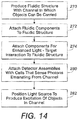
- Fig. 14 illustrates exemplary operations in producing an analyzer like analyzer 10 in Fig. 1 .
- the operation in box 270 produces a fluidic structure with a channel in a portion of which objects can be carried by fluid.
- the operation in box 270 could include manufacturing a fluidic structure by positioning or otherwise producing a structured spacer layer between two quartz slides.
- the spacer layer could be a patterned layer of PDMS or could be any other suitable material or combination of materials, including, for example, Gelfilm® or quartz.
- the operation in box 270 could alternatively be implemented in various other ways, such as by defining a fluidic channel in a quartz slide by glass etching or by molding PDMS to produce a channel, and by then combining the resulting structure with an upper quartz slide.
- Two layers of PDMS could be fabricated on separate substrates and then one could be flipped over and aligned with the other by chip-on-chip assembly.
- a final substrate of glass, PCB, or PDMS or sufficient hardness could be used to allow direction connection to control and detection measurement circuitry.
- the operation in box 270 can include positioning gel or other material within channel 14. This operation involves positioning the material so that light can enter one portion of the channel at a first angle oblique to the longitudinal direction, pass through the bounding component, and enter another portion of the channel at a second angle oblique to the longitudinal direction.
- the operation in box 270 can include closing off the ends of a channel with end components such as gel. Also, entry and exit ports can be provided.
- the operation in box 272 then attaches fluidic components to the fluidic structure.
- the fluidic components attached in box 272 can be operated to cause and control movement of objects in the channel.
- the operation in box 274 attaches components for enhanced light-target interaction.
- the operation in box 274 can attach optical component 96 on the side of support layer 90, providing an appropriate surface through which light can be coupled into a portion of channel 14 that functions as an anti-resonant waveguide.
- the operation in box 274 can produce spacers 72 to provide a suitable gap that avoids interference with anti-resonant wave guiding.
- the IC in detector 87 is later attached with gap 88 between it and the fluidic structure, the IC does not interfere with propagation of light in channel 14.
- the operation in box 280 attaches photosensor arrays with cells that sense photons emanating from channel 14.
- the operation in box 280 can be implemented by attaching detector 87, such as with cells that sense in different subranges and with reference cells.
- each light source can be attached once, after which it is stationary.
- one or more light sources are positioned to produce excitation of objects being carried within the channel.
- Fig. 14 could be modified.
- the operations in boxes 272, 274, 280, and 282 could be combined in any appropriate way to facilitate attachment of components in a desired sequence.
- An additional operation could be performed to align or attach interconnects between ICs, gates, and other circuitry, such as connectors to a microprocessor or computer, or this operation could be partially performed in each of boxes 272, 274, 280, and 282.
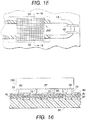
- Fig. 15 shows an alternative arrangement that could be produced by an implementation of Fig. 14 .
- First and second fluorescence sensing components 56 and 58 are next to each other in the series of sensing components along channel 14. In addition, however, they are positioned so that IC 290 can be attached over both of them.
- the photosensor array of IC 290 includes both cells along channel 14 within component 56 and also cells along channel 14 within component 58.
- Fig. 16 is a cross section along the line 16-16 in Fig. 15 , and shows how detector 292 which includes IC 290, can be supported over air gap 88 by spacers 72.
- the lateral variation in optical thickness of the transmission structure may be such that the ranges and subranges photosensed within sensing component 56 are different from those photosensed within sensing component 58; alternatively, the ranges and subranges could be the same.
- Spacers 72 can help to reduce cross-talk between components 56 and 58 because spacers 72 can be shaped and positioned to act as light-absorbing walls between the two components.
- Fig. 17 shows an alternative arrangement in which detector 292 as in Fig. 14 is positioned over a set of parallel channels 294, which could be produced by producing walls 296 to subdivide a larger channel into subchannels. Laterally varying optical thicknesses of a transmission structure can be produced so that a different range of photon energies is photosensed in each of channels 294, or different subranges are photosensed in different channels, or the same ranges and subranges could be photosensed in all channels.
- FIG. 18 shows an alternative arrangement.
- Portion 80 of channel 14 functions as an anti-resonant waveguide in response to light from source 84.
- Assembly 87 is along portion 80, separated from plate 94 by spacers 72. Upstream from portion 80 (but downstream from light source 84) can be positioned a series of triggering photodetectors, represented by photodetector 300 on spacers 302.
- fluorescing objects 310, 312, and 314 are being carried through channel 14. As they fluoresce, objects 310, 312, and 314 emanate photons, represented respectively by rays 320, 322, and 324. Quantities read out from a photosensor array in detector 87 can be used to obtain information about objects 310, 312, and 314 even though all three objects are concurrently traveling past the array.
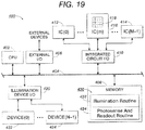
- Fig. 19 illustrates system 400 with central processing unit (CPU) 402 connected to various components through bus 404.
- CPU central processing unit
- System 400 also includes external input/output (I/O) component 406 and memory 408, both connected to bus 404.
- I/O 406 permits CPU 402 to communicate with devices outside of system 400.
- IC I/O 410 is a component that permits CPU 402 to communicate with ICs in analyzer 10; M ICs are illustrated in Fig. 19 by a series extending from IC(0) 412 to IC (M-1) 414. ICs 412 through 414 illustratively include IC(m) 416 with a photosensor array 418, which includes cells that photosense subranges as described above.
- illumination device I/O 420 is a component permitting CPU 402 to communicate with various illumination devices; N illumination devices are represented in Fig. 19 by device (0) 422 through device (N-1) 424.
- Memory 408 includes program memory 430.
- the routines stored in program memory 430 illustratively include illumination routine 432 and photosense and readout routine 434.
- CPU 402 can execute illumination routine 432 to communicate with light sources 84 and 244.
- CPU 402 can receive signals from sensors, perform computations to determine what illumination operations are necessary, and then provide signals to activate light sources 84 and 244.
- CPU 402 can execute photosense and readout routine 434 to obtain information from cells in ICs 412 through 414, which can include ICs 64, 66, 68, 70, 252, and 290, as described above.
- CPU 402 can provide signals so that photosensing is performed during an appropriate sensing period, after which signals are received from the cells of an IC by CPU 402.
- the exemplary implementations described above provide various ways of producing enhanced light-target interaction in a channel or channel portion and sensing of photons that emanate as a result.
- the exemplary implementations can be used to provide coupling to anti-resonant waveguide modes of a channel or channel portion, including where illumination through end facets is not feasible.
- the exemplary implementations described above can provide compact, inexpensive components that generally require no additional mechanical or optical parts to perform functions such as spectrometry.
- the results of photosensing can be read out rapidly and in parallel from a number of ICs, allowing fast data acquisition; as a result, an initial characterization of an object may be used to determine whether to perform more refined or detailed analysis of the object, or to determine which of different types of analysis are performed.
- a multi-signal approach like this is compatible with reagentless identification; also, a wide variety of objects can be identified in a wide variety of fluids.
- the implementations generally permit a continuous flow of analytes through an analyzer, allowing real-time analysis and the possibility of interactive detection schemes.
- Spectrometry measurements have a wide variety of applications, including, for example, optical instrumentation, telecommunications, fluorescence devices, process control, optical signal scanning, detection systems for chemical and biological agents, and so forth.
- An example of a specific application is an in-line detector for manufacturing and functionalizing colloidal particles in an industrial setting.
- processes typically are performed in closed systems and the properties of colloidal particles can be assessed only after all processing steps are completed.
- a small detection platform implemented as described above can be easily built into an on-line detector directly connected to a manufacturing vessel. As a result, small amounts of particles can be analyzed continuously in real time to determine size, chemical composition, and surface conditions. This approach permits instant process adjustments leading to production of materials with consistent properties from run to run.
- In-line Coulter counters for instant size measurements are already commercially available, but compact detectors as described above can also probe chemical composition using multiple advanced spectroscopic methods, an approach not previously available.
- absorption spectroscopy e.g. gas sensing
- fluorescence spectroscopy e.g. fluorescence spectroscopy
- Raman spectroscopy e.g. Raman spectroscopy
- Components could have other various shapes, dimensions, or other numerical or qualitative characteristics
- ICs relative to fluidic structures could be made, with any other suitable type of photosensor or other devices.
- objects could be photosensed one at a time, the techniques described above also allow concurrent photosensing of multiple objects.
- a preliminary inspection of an analyte could be made with an IC with a 400-700 nm laterally varying filter to detect fluorescence or scattering in the 400-700 nm range, after which a more refined inspection could be made with another IC, such as to perform Raman spectroscopy in the range of 100 cm -1 to a few 1000 cm -1 .
- different rows of a single two-dimensional photosensor array on an IC could be differently coated to photosense in different ranges.
- a CPU which could be a microprocessor or any other appropriate component.
Claims (4)
- Appareil comprenant :une structure fluidique (12) ; etdéfinie à l'intérieur de la structure fluidique, une partie de canal (14) s'étendant dans une direction longitudinale et ayant, dans chaque position le long de sa longueur, une section transversale respective ; dans chaque section transversale de la position, la partie de canal a une limite (90, 94, 122, 124) le long de la majeure partie de laquelle, elle est entourée par un matériau ayant un indice de réfraction supérieur à un liquide ;la structure fluidique comprenant :un composant de délimitation de transmission de lumière (184, 200) configuré pour conserver une barrière fluidique entre les première (180) et seconde (182) parties du canal ; la structure fluidique ayant en outre, définis à l'intérieur de cette dernière, deux orifices (150, 152) à travers lesquels un fluide peut entrer et sortir de la première partie (180) ; etune couche de transmission de lumière (94) qui s'étend dans la direction longitudinale le long d'au moins une partie de la limite de la première partie et au-delà du composant de délimitation (184, 200) jusqu'à la seconde partie (182) ;dans lequel la couche (94) et le composant de délimitation (184, 200) sont positionnés de sorte que la lumière peut entrer dans la seconde partie (182) à partir du composant allongé (94) à un premier angle d'incidence par rapport à la direction longitudinale, traverser le composant de délimitation (184, 200) et entrer dans la seconde partie (180) du canal (14) à un second angle d'incidence par rapport à la direction longitudinale, le second angle étant inférieur au premier angle ;dans lequel la structure fluidique (12) comprend en outre un composant externe (160) dans la seconde partie (182) du canal et à l'extérieur du composant de délimitation (184, 200), la seconde partie (182) contenant de l'air, du gaz ou du vide entre le composant externe (160) et le composant de délimitation (184, 200).
- Appareil selon la revendication 1, dans lequel le second angle est d'approximativement 2° ou moins.
- Appareil selon la revendication 1 ou la revendication 2, configuré de sorte que la lumière pénétrant dans la première partie (180) du canal au second angle est adaptée pour se coupler à un mode de guide d'onde anti-résonant de la première partie.
- Procédé pour détecter des photons émanant de la partie de canal (14) définie dans la structure fluidique (12) de l'appareil selon l'une quelconque des revendications 1 à 3, le procédé comprenant les étapes suivantes :avec du liquide dans la partie de canal (14), propager la lumière dans la direction longitudinale à travers la partie de canal de sorte que, dans les sections transversales le long d'une partie de la longueur, plus d'approximativement 10 % d'intensité lumineuse de la lumière propagée apparaissent dans le liquide ;l'acte de propager la lumière comprenant :fournir la lumière à partir d'une source à l'extérieur de la partie de canal (14) à travers le composant allongé de transmission de lumière à un premier angle oblique par rapport à la direction longitudinale, à travers la seconde partie (182) et à travers le composant de délimitation de transmission de lumière (184, 200) ; la lumière provenant de la source (84) pénétrant dans la première partie (180) à un second angle oblique par rapport à la direction longitudinale, le second angle étant inférieur au premier angle ; etdétecter des photons émanant de la partie de canal (14) en réponse à la lumière propagée.
Applications Claiming Priority (1)
| Application Number | Priority Date | Filing Date | Title |
|---|---|---|---|
| US11/316,660 US7386199B2 (en) | 2005-12-22 | 2005-12-22 | Providing light to channels or portions |
Publications (2)
| Publication Number | Publication Date |
|---|---|
| EP1801564A1 EP1801564A1 (fr) | 2007-06-27 |
| EP1801564B1 true EP1801564B1 (fr) | 2018-06-20 |
Family
ID=37876922
Family Applications (1)
| Application Number | Title | Priority Date | Filing Date |
|---|---|---|---|
| EP06126528.6A Expired - Fee Related EP1801564B1 (fr) | 2005-12-22 | 2006-12-19 | Dispositif et procédé pour la fourniture de lumière aux canaux ou portions |
Country Status (3)
| Country | Link |
|---|---|
| US (1) | US7386199B2 (fr) |
| EP (1) | EP1801564B1 (fr) |
| JP (1) | JP5160776B2 (fr) |
Families Citing this family (57)
| Publication number | Priority date | Publication date | Assignee | Title |
|---|---|---|---|---|
| US7310153B2 (en) | 2004-08-23 | 2007-12-18 | Palo Alto Research Center, Incorporated | Using position-sensitive detectors for wavelength determination |
| US7522786B2 (en) * | 2005-12-22 | 2009-04-21 | Palo Alto Research Center Incorporated | Transmitting light with photon energy information |
| US8437582B2 (en) * | 2005-12-22 | 2013-05-07 | Palo Alto Research Center Incorporated | Transmitting light with lateral variation |
| US7358476B2 (en) * | 2005-12-22 | 2008-04-15 | Palo Alto Research Center Incorporated | Sensing photons from objects in channels |
| US7547904B2 (en) * | 2005-12-22 | 2009-06-16 | Palo Alto Research Center Incorporated | Sensing photon energies emanating from channels or moving objects |
| US7315667B2 (en) * | 2005-12-22 | 2008-01-01 | Palo Alto Research Center Incorporated | Propagating light to be sensed |
| US7386199B2 (en) | 2005-12-22 | 2008-06-10 | Palo Alto Research Center Incorporated | Providing light to channels or portions |
| US7420677B2 (en) * | 2005-12-22 | 2008-09-02 | Palo Alto Research Center Incorporated | Sensing photon energies of optical signals |
| US7718948B2 (en) * | 2006-12-04 | 2010-05-18 | Palo Alto Research Center Incorporated | Monitoring light pulses |
| US8821799B2 (en) | 2007-01-26 | 2014-09-02 | Palo Alto Research Center Incorporated | Method and system implementing spatially modulated excitation or emission for particle characterization with enhanced sensitivity |
| US9164037B2 (en) | 2007-01-26 | 2015-10-20 | Palo Alto Research Center Incorporated | Method and system for evaluation of signals received from spatially modulated excitation and emission to accurately determine particle positions and distances |
| US7936463B2 (en) | 2007-02-05 | 2011-05-03 | Palo Alto Research Center Incorporated | Containing analyte in optical cavity structures |
| US7545513B2 (en) * | 2007-02-05 | 2009-06-09 | Palo Alto Research Center Incorporated | Encoding optical cavity output light |
| US7817276B2 (en) | 2007-02-05 | 2010-10-19 | Palo Alto Research Center Incorporated | Distinguishing objects |
| US7554673B2 (en) * | 2007-02-05 | 2009-06-30 | Palo Alto Research Center Incorporated | Obtaining information about analytes using optical cavity output light |
| US7633629B2 (en) | 2007-02-05 | 2009-12-15 | Palo Alto Research Center Incorporated | Tuning optical cavities |
| US7502123B2 (en) * | 2007-02-05 | 2009-03-10 | Palo Alto Research Center Incorporated | Obtaining information from optical cavity output light |
| US7522811B2 (en) * | 2007-07-13 | 2009-04-21 | Palo Alto Research Center Incorporated | Producing sandwich waveguides |
| US7529438B2 (en) * | 2007-07-13 | 2009-05-05 | Palo Alto Research Center Incorporated | Producing fluidic waveguides |
| US7822300B2 (en) * | 2007-11-20 | 2010-10-26 | Aptina Imaging Corporation | Anti-resonant reflecting optical waveguide for imager light pipe |
| US8320983B2 (en) * | 2007-12-17 | 2012-11-27 | Palo Alto Research Center Incorporated | Controlling transfer of objects affecting optical characteristics |
| US8153949B2 (en) * | 2008-12-18 | 2012-04-10 | Palo Alto Research Center Incorporated | Obtaining sensing results indicating time variation |
| US8153950B2 (en) * | 2008-12-18 | 2012-04-10 | Palo Alto Research Center Incorporated | Obtaining sensing results and/or data in response to object detection |
| US7763856B2 (en) * | 2008-01-31 | 2010-07-27 | Palo Alto Research Center Incorporated | Producing time variation in emanating light |
| EP2085760B1 (fr) | 2008-01-30 | 2018-07-04 | Palo Alto Research Center Incorporated | Génération de variation temporelle dans l'émission de lumière |
| US7701580B2 (en) * | 2008-02-01 | 2010-04-20 | Palo Alto Research Center Incorporated | Transmitting/reflecting emanating light with time variation |
| EP2085761B1 (fr) | 2008-01-30 | 2018-11-28 | Palo Alto Research Center Incorporated | Obtention de résultats de détection indiquant une variation temporelle |
| JP5541764B2 (ja) | 2008-01-30 | 2014-07-09 | パロ・アルト・リサーチ・センター・インコーポレーテッド | 物体検出に応答して情報を取得する装置及び方法 |
| US7817254B2 (en) | 2008-01-30 | 2010-10-19 | Palo Alto Research Center Incorporated | Obtaining information from time variation of sensing results |
| EP2085758B1 (fr) * | 2008-01-30 | 2014-06-04 | Palo Alto Research Center Incorporated | Génération de mouvement relatif |
| EP2085797B1 (fr) | 2008-01-30 | 2016-06-01 | Palo Alto Research Center Incorporated | Production de filtres avec des fonctions de transmission et/ou de réflexion combinées |
| US7894068B2 (en) * | 2008-02-04 | 2011-02-22 | Palo Alto Research Center Incorporated | Producing filters with combined transmission and/or reflection functions |
| EP2085762B1 (fr) | 2008-01-30 | 2018-07-04 | Palo Alto Research Center Incorporated | Transmission/réflexion de lumière d'émission avec une variation temporelle |
| US8373860B2 (en) * | 2008-02-01 | 2013-02-12 | Palo Alto Research Center Incorporated | Transmitting/reflecting emanating light with time variation |
| US8629981B2 (en) | 2008-02-01 | 2014-01-14 | Palo Alto Research Center Incorporated | Analyzers with time variation based on color-coded spatial modulation |
| US8586347B2 (en) | 2010-09-15 | 2013-11-19 | Mbio Diagnostics, Inc. | System and method for detecting multiple molecules in one assay |
| US8331751B2 (en) * | 2009-03-02 | 2012-12-11 | mBio Diagnositcs, Inc. | Planar optical waveguide with core of low-index-of-refraction interrogation medium |
| US9658222B2 (en) | 2009-03-02 | 2017-05-23 | Mbio Diagnostics, Inc. | Planar waveguide based cartridges and associated methods for detecting target analyte |
| US9212995B2 (en) | 2009-03-02 | 2015-12-15 | Mbio Diagnostics, Inc. | System and method for detecting multiple molecules in one assay |
| JP4927197B2 (ja) * | 2010-06-01 | 2012-05-09 | シャープ株式会社 | マイクロ分析チップ、該マイクロ分析チップを用いた分析装置、及び送液方法 |
| GB201016270D0 (en) * | 2010-09-28 | 2010-11-10 | Univ St Andrews | Waveguide localised raman spectroscopy |
| US10114020B2 (en) | 2010-10-11 | 2018-10-30 | Mbio Diagnostics, Inc. | System and device for analyzing a fluidic sample |
| US9029800B2 (en) | 2011-08-09 | 2015-05-12 | Palo Alto Research Center Incorporated | Compact analyzer with spatial modulation and multiple intensity modulated excitation sources |
| US8723140B2 (en) | 2011-08-09 | 2014-05-13 | Palo Alto Research Center Incorporated | Particle analyzer with spatial modulation and long lifetime bioprobes |
| JP5988690B2 (ja) * | 2012-05-18 | 2016-09-07 | 浜松ホトニクス株式会社 | 分光センサ |
| JP5875936B2 (ja) | 2012-05-18 | 2016-03-02 | 浜松ホトニクス株式会社 | 分光センサ |
| US9739714B2 (en) | 2012-10-29 | 2017-08-22 | Mbio Diagnostics, Inc. | Particle identification system, cartridge and associated methods |
| US9551617B2 (en) * | 2013-07-11 | 2017-01-24 | Shimadzu Corporation | Raman spectroscopic analyzer |
| US9952033B2 (en) | 2014-02-14 | 2018-04-24 | Palo Alto Research Center Incorporated | Spatial modulation of light to determine object length |
| US10451482B2 (en) | 2014-02-14 | 2019-10-22 | Palo Alto Research Center Incorporated | Determination of color characteristics of objects using spatially modulated light |
| US9207066B2 (en) | 2014-02-14 | 2015-12-08 | Palo Alto Research Center Incorporated | Spatial modulation of light to determine dimensional characteristics of objects in a flow path |
| US9528925B2 (en) * | 2014-02-14 | 2016-12-27 | Palo Alto Research Center Incorporated | Spatial modulation of light to determine object position |
| US9400174B2 (en) | 2014-04-07 | 2016-07-26 | Palo Alto Research Center Incorporated | Monitor for particle injector |
| US9114606B1 (en) | 2014-04-07 | 2015-08-25 | Palo Alto Research Center Incorporated | Spatial light modulation method for determining droplet motion characteristics |
| DE102018118484B4 (de) * | 2018-07-31 | 2021-09-16 | Institut für Bioprozess- und Analysenmesstechnik e.V. | Vorrichtung und Verfahren zur optischen Charakterisierung von Fluiden und/oder darin eingeschlossener Objekte in Mikrokanälen |
| US10458909B1 (en) | 2018-10-24 | 2019-10-29 | International Business Machines Corporation | MEMS optical sensor |
| US20230175891A1 (en) * | 2021-12-08 | 2023-06-08 | Battelle Savannah River Alliance, Llc | Electric field detection method and system |
Citations (1)
| Publication number | Priority date | Publication date | Assignee | Title |
|---|---|---|---|---|
| US3797911A (en) * | 1972-10-18 | 1974-03-19 | Bell Telephone Labor Inc | Thin film optical couplers employing mode conversion |
Family Cites Families (101)
| Publication number | Priority date | Publication date | Assignee | Title |
|---|---|---|---|---|
| US2708389A (en) * | 1951-01-09 | 1955-05-17 | Frederick W Kavanagh | Spectral wedge interference filter combined with purifying filters |
| US3973118A (en) * | 1975-03-25 | 1976-08-03 | Lamontagne Joseph Alfred | Electro-optical detector array and spectrum analyzer system |
| US4081277A (en) * | 1976-10-08 | 1978-03-28 | Eastman Kodak Company | Method for making a solid-state color imaging device having an integral color filter and the device |
| SE450528B (sv) * | 1981-03-19 | 1987-06-29 | Svenska Traeforskningsinst | Forfarande for metning av innehallet av kryll i pappersmassa |
| US4573796A (en) * | 1984-01-06 | 1986-03-04 | The United States Of America As Represented By The United States Department Of Energy | Apparatus for eliminating background interference in fluorescence measurements |
| US4715672A (en) * | 1986-01-06 | 1987-12-29 | American Telephone And Telegraph Company | Optical waveguide utilizing an antiresonant layered structure |
| CA1293879C (fr) * | 1986-06-20 | 1992-01-07 | Laurel Jean Pace | Reseaux de filtres couleur |
| US4957371A (en) * | 1987-12-11 | 1990-09-18 | Santa Barbara Research Center | Wedge-filter spectrometer |
| US4976542A (en) * | 1988-07-25 | 1990-12-11 | Washington University | Digital array scanned interferometer |
| JPH0249143A (ja) * | 1988-08-11 | 1990-02-19 | Ngk Spark Plug Co Ltd | 混合液体の液体混合比検出器 |
| JPH0249144A (ja) * | 1988-08-11 | 1990-02-19 | Ngk Spark Plug Co Ltd | 混合液体の液体混合比検出器 |
| US5080462A (en) * | 1989-11-02 | 1992-01-14 | Fuji Photo Film Co., Ltd. | Optical wavelength converter device and optical wavelength converter system |
| US5144498A (en) * | 1990-02-14 | 1992-09-01 | Hewlett-Packard Company | Variable wavelength light filter and sensor system |
| US5166755A (en) * | 1990-05-23 | 1992-11-24 | Nahum Gat | Spectrometer apparatus |
| US5784507A (en) * | 1991-04-05 | 1998-07-21 | Holm-Kennedy; James W. | Integrated optical wavelength discrimination devices and methods for fabricating same |
| US5184192A (en) * | 1991-07-17 | 1993-02-02 | Millipore Corporation | Photometric apparatus with a flow cell coated with an amorphous fluoropolymer |
| US5370842A (en) * | 1991-11-29 | 1994-12-06 | Canon Kabushiki Kaisha | Sample measuring device and sample measuring system |
| US5305082A (en) * | 1992-01-08 | 1994-04-19 | Chromax, Inc. | High spatial resolution imaging spectrograph |
| US5324401A (en) * | 1993-02-05 | 1994-06-28 | Iowa State University Research Foundation, Inc. | Multiplexed fluorescence detector system for capillary electrophoresis |
| US5494798A (en) * | 1993-12-09 | 1996-02-27 | Gerdt; David W. | Fiber optic evanscent wave sensor for immunoassay |
| WO1995020144A1 (fr) | 1994-01-20 | 1995-07-27 | British Telecommunications Public Limited Company | Capteur de longueurs d'ondes optiques |
| DE69405087T2 (de) * | 1994-04-27 | 1997-12-18 | Hewlett Packard Gmbh | Optischer Detektor |
| US6199257B1 (en) * | 1995-02-28 | 2001-03-13 | Thermo Separation Products, Inc. | Method of making a flow cell for light absorption measurement of small volume samples |
| US5682038A (en) * | 1995-04-06 | 1997-10-28 | Becton Dickinson And Company | Fluorescent-particle analyzer with timing alignment for analog pulse subtraction of fluorescent pulses arising from different excitation locations |
| US5777329A (en) * | 1995-07-21 | 1998-07-07 | Texas Instruments Incorporated | Bolometer array spectrometer |
| DE69524405T2 (de) * | 1995-09-06 | 2002-05-23 | Agilent Technologies Deutschla | Photometrische Durchflussvorrichtung für kleine Probenvolumina |
| EP0928416A4 (fr) * | 1996-03-19 | 2000-03-29 | Univ Utah Res Found | Lentille et cuve a flux continu associee |
| US5770156A (en) * | 1996-06-04 | 1998-06-23 | In Usa, Inc. | Gas detection and measurement system |
| US5801831A (en) * | 1996-09-20 | 1998-09-01 | Institute For Space And Terrestrial Science | Fabry-Perot spectrometer for detecting a spatially varying spectral signature of an extended source |
| US5792663A (en) * | 1996-09-27 | 1998-08-11 | Transgenomic Incorporated | High efficiency continuous flow through fractional-volatilization separator system, and method of use |
| EP0938660B1 (fr) * | 1996-11-18 | 2000-04-12 | Fraunhofer-Gesellschaft Zur Förderung Der Angewandten Forschung E.V. | Cellule micromecanique de mesure de transmission |
| US5864641A (en) * | 1997-04-11 | 1999-01-26 | F&S, Inc. | Optical fiber long period sensor having a reactive coating |
| US6238348B1 (en) * | 1997-07-22 | 2001-05-29 | Scimed Life Systems, Inc. | Miniature spectrometer system and method |
| US5880474A (en) * | 1997-08-29 | 1999-03-09 | Becton Dickinson And Company | Multi-illumination-source flow particle analyzer with inter-location emissions crosstalk cancelation |
| DE19754910C2 (de) * | 1997-12-10 | 1999-12-02 | Geoforschungszentrum Potsdam | Wellenlängendetektion an Faser-Bragg-Gitter-Sensoren |
| GB9803704D0 (en) | 1998-02-24 | 1998-04-15 | Univ Manchester | Waveguide structure |
| US6719868B1 (en) * | 1998-03-23 | 2004-04-13 | President And Fellows Of Harvard College | Methods for fabricating microfluidic structures |
| US6459080B1 (en) * | 1998-06-12 | 2002-10-01 | Agilent Technologies, Inc. | Miniaturized device for separating the constituents of a sample and delivering the constituents of the separated sample to a mass spectrometer |
| DE59915204D1 (de) * | 1998-08-28 | 2010-10-28 | Febit Holding Gmbh | Verfahren zur herstellung von biochemischen reaktionsträgern |
| US6275628B1 (en) * | 1998-12-10 | 2001-08-14 | Luna Innovations, Inc. | Single-ended long period grating optical device |
| US6399405B1 (en) * | 1998-12-21 | 2002-06-04 | Xerox Corporation | Process for constructing a spectrophotometer |
| US6608679B1 (en) * | 1998-12-21 | 2003-08-19 | Xerox Corporation | Spectrophotometric analysis of input light |
| US6249346B1 (en) * | 1998-12-21 | 2001-06-19 | Xerox Corporation | Monolithic spectrophotometer |
| EP1031828B1 (fr) * | 1999-02-25 | 2006-09-13 | C.S.E.M. Centre Suisse D'electronique Et De Microtechnique Sa | Capteur en optique intégrée et méthode pour déterminer en optique intégrée une substance |
| US6558945B1 (en) * | 1999-03-08 | 2003-05-06 | Aclara Biosciences, Inc. | Method and device for rapid color detection |
| US6455833B1 (en) * | 1999-03-09 | 2002-09-24 | Micron Technology, Inc. | Superposed multi-junction color APS |
| JP3530078B2 (ja) * | 1999-07-06 | 2004-05-24 | リオン株式会社 | フローセル及びこのフローセルを用いた粒子測定装置 |
| US6192168B1 (en) * | 1999-04-09 | 2001-02-20 | The United States Of America As Represented By The Secretary Of The Navy | Reflectively coated optical waveguide and fluidics cell integration |
| AU4128500A (en) | 1999-04-09 | 2000-11-14 | University Of Manchester Institute Of Science & Technology, The | Electrophoresis method and apparatus with time- or space-modulated sample injection |
| US6137117A (en) * | 1999-06-21 | 2000-10-24 | The United States Of America As Represented By The Secretary Of The Navy | Integrating multi-waveguide sensor |
| US6353475B1 (en) * | 1999-07-12 | 2002-03-05 | Caliper Technologies Corp. | Light source power modulation for use with chemical and biochemical analysis |
| US6495104B1 (en) * | 1999-08-19 | 2002-12-17 | Caliper Technologies Corp. | Indicator components for microfluidic systems |
| US6216022B1 (en) * | 2000-06-22 | 2001-04-10 | Biosafe Laboratories, Inc. | Implantable optical measurement device and method for using same |
| US7167615B1 (en) * | 1999-11-05 | 2007-01-23 | Board Of Regents, The University Of Texas System | Resonant waveguide-grating filters and sensors and methods for making and using same |
| US6603548B2 (en) * | 1999-12-03 | 2003-08-05 | Sciperio, Inc. | Biosensor |
| US6295130B1 (en) * | 1999-12-22 | 2001-09-25 | Xerox Corporation | Structure and method for a microelectromechanically tunable fabry-perot cavity spectrophotometer |
| US6519037B2 (en) * | 1999-12-23 | 2003-02-11 | Lj Laboratories, Llc | Spectrometer having optical unit including a randomized fiber optic implement |
| US6580507B2 (en) * | 2000-03-02 | 2003-06-17 | Sd Acquisition Inc. | Single source, single detector chip, multiple-longitudinal channel electromagnetic radiation absorbance and fluorescence monitoring system |
| US6569383B1 (en) * | 2000-03-11 | 2003-05-27 | Intrinsic Bioprobes, Inc. | Bioactive chip mass spectrometry |
| US6505775B1 (en) * | 2000-04-25 | 2003-01-14 | Ncr Corporation | Produce data collector with enhanced LVF spectrometer |
| EP1327135B1 (fr) * | 2000-09-04 | 2010-02-24 | Bayer Technology Services GmbH | Systeme et procedes pour determiner plusieurs analytes |
| GB0023041D0 (en) | 2000-09-20 | 2000-11-01 | Univ Manchester | Identification apparatus |
| WO2002025934A2 (fr) * | 2000-09-25 | 2002-03-28 | Sensovation Ag | Dispositif de detection d'images, appareil et procede de mesures optiques |
| US7217574B2 (en) * | 2000-10-30 | 2007-05-15 | Sru Biosystems, Inc. | Method and apparatus for biosensor spectral shift detection |
| US7264973B2 (en) * | 2000-10-30 | 2007-09-04 | Sru Biosystems, Inc. | Label-free methods for performing assays using a colorimetric resonant optical biosensor |
| US6577780B2 (en) * | 2001-03-08 | 2003-06-10 | Veridian Systems | Cell designs for optical biosensors |
| US6785002B2 (en) * | 2001-03-16 | 2004-08-31 | Optical Coating Laboratory, Inc. | Variable filter-based optical spectrometer |
| US6630999B2 (en) * | 2001-05-01 | 2003-10-07 | Optical Coating Laboratory, Inc. | Color measuring sensor assembly for spectrometer devices |
| DE50105368D1 (de) * | 2001-06-28 | 2005-03-24 | Agilent Technologies Inc | Mikrofluid-System mit Regler |
| US6934435B2 (en) * | 2001-10-05 | 2005-08-23 | ARETé ASSOCIATES | Microfluidic pump system for chemical or biological agents |
| US20050042615A1 (en) * | 2001-11-02 | 2005-02-24 | Smith William Ewen | Microfluidic ser(r)s detection |
| US6800849B2 (en) * | 2001-12-19 | 2004-10-05 | Sau Lan Tang Staats | Microfluidic array devices and methods of manufacture and uses thereof |
| US7524459B2 (en) * | 2002-01-24 | 2009-04-28 | California Institute Of Technology In Pasadena | Optoelectronic and microfluidic integration for miniaturized spectroscopic devices |
| WO2003073069A1 (fr) * | 2002-02-25 | 2003-09-04 | Waters Investments Limited | Additif opaque servant a bloquer la lumiere parasite dans des cuves a circulation en teflon af guidant la lumiere |
| JP2003279471A (ja) * | 2002-03-20 | 2003-10-02 | Nippon Sheet Glass Co Ltd | マイクロ化学システム用チップ及びマイクロ化学システム |
| US6867420B2 (en) * | 2002-06-03 | 2005-03-15 | The Regents Of The University Of California | Solid-state detector and optical system for microchip analyzers |
| US6700664B1 (en) * | 2002-08-15 | 2004-03-02 | Jds Uniphase Corporation | Optical channel monitoring device |
| DE60212620T2 (de) * | 2002-08-16 | 2006-11-02 | Agilent Technologies, Inc. (n.d.Ges.d.Staates Delaware), Palo Alto | Verfahren und Vorrichtung zum Analysieren eines Probenstoffgemischs |
| US20040067167A1 (en) | 2002-10-08 | 2004-04-08 | Genoptix, Inc. | Methods and apparatus for optophoretic diagnosis of cells and particles |
| US7106441B2 (en) * | 2002-10-28 | 2006-09-12 | Xerox Corporation | Structure and method for a microelectromechanic cylindrical reflective diffraction grating spectrophotometer |
| US7064836B2 (en) * | 2003-04-21 | 2006-06-20 | The Board Of Trustees Of The Leland Stanford Junior University | Brewster's angle flow cell for cavity ring-down spectroscopy |
| US7497992B2 (en) * | 2003-05-08 | 2009-03-03 | Sru Biosystems, Inc. | Detection of biochemical interactions on a biosensor using tunable filters and tunable lasers |
| WO2004111586A1 (fr) * | 2003-05-27 | 2004-12-23 | Wayne State University | Spectrometre d'imagerie de diffraction |
| US7149396B2 (en) * | 2003-06-16 | 2006-12-12 | The Regents Of The University Of California | Apparatus for optical measurements on low-index non-solid materials based on arrow waveguides |
| US7298478B2 (en) * | 2003-08-14 | 2007-11-20 | Cytonome, Inc. | Optical detector for a particle sorting system |
| JP2005170803A (ja) * | 2003-12-08 | 2005-06-30 | Daicel Chem Ind Ltd | 新規なマロン酸モノメチル誘導体とその製造法 |
| EP1773493B1 (fr) | 2004-07-22 | 2008-12-10 | Agilent Technologies, Inc. | Agencement microfluidique pour detection optique microfluidique |
| US7310153B2 (en) * | 2004-08-23 | 2007-12-18 | Palo Alto Research Center, Incorporated | Using position-sensitive detectors for wavelength determination |
| US7522786B2 (en) | 2005-12-22 | 2009-04-21 | Palo Alto Research Center Incorporated | Transmitting light with photon energy information |
| US7291824B2 (en) * | 2005-12-22 | 2007-11-06 | Palo Alto Research Center Incorporated | Photosensing throughout energy range and in subranges |
| US7387892B2 (en) * | 2004-09-01 | 2008-06-17 | Palo Alto Research Center Incorporated | Biosensor using microdisk laser |
| US7268868B2 (en) * | 2004-10-29 | 2007-09-11 | Palo Alto Research Center Incorporated | Anti-resonant waveguide sensors |
| US7811438B2 (en) * | 2004-12-08 | 2010-10-12 | Palo Alto Research Center Incorporated | Bio-enrichment device to enhance sample collection and detection |
| US7466409B2 (en) | 2005-06-08 | 2008-12-16 | California Institute Of Technology | Method and apparatus for CMOS imagers and spectroscopy |
| US7547904B2 (en) | 2005-12-22 | 2009-06-16 | Palo Alto Research Center Incorporated | Sensing photon energies emanating from channels or moving objects |
| US7358476B2 (en) | 2005-12-22 | 2008-04-15 | Palo Alto Research Center Incorporated | Sensing photons from objects in channels |
| US7248361B2 (en) * | 2005-12-22 | 2007-07-24 | Palo Alto Research Center Incorporated | Fluorescence reader based on anti-resonant waveguide excitation |
| US7420677B2 (en) * | 2005-12-22 | 2008-09-02 | Palo Alto Research Center Incorporated | Sensing photon energies of optical signals |
| US7386199B2 (en) | 2005-12-22 | 2008-06-10 | Palo Alto Research Center Incorporated | Providing light to channels or portions |
| US7433552B2 (en) | 2005-12-22 | 2008-10-07 | Palo Alto Research Center Incorporated | Obtaining analyte information |
| US7315667B2 (en) * | 2005-12-22 | 2008-01-01 | Palo Alto Research Center Incorporated | Propagating light to be sensed |
-
2005
- 2005-12-22 US US11/316,660 patent/US7386199B2/en active Active
-
2006
- 2006-12-18 JP JP2006339568A patent/JP5160776B2/ja not_active Expired - Fee Related
- 2006-12-19 EP EP06126528.6A patent/EP1801564B1/fr not_active Expired - Fee Related
Patent Citations (1)
| Publication number | Priority date | Publication date | Assignee | Title |
|---|---|---|---|---|
| US3797911A (en) * | 1972-10-18 | 1974-03-19 | Bell Telephone Labor Inc | Thin film optical couplers employing mode conversion |
Also Published As
| Publication number | Publication date |
|---|---|
| JP5160776B2 (ja) | 2013-03-13 |
| JP2007171182A (ja) | 2007-07-05 |
| EP1801564A1 (fr) | 2007-06-27 |
| US7386199B2 (en) | 2008-06-10 |
| US20070147728A1 (en) | 2007-06-28 |
Similar Documents
| Publication | Publication Date | Title |
|---|---|---|
| EP1801564B1 (fr) | Dispositif et procédé pour la fourniture de lumière aux canaux ou portions | |
| US7479625B2 (en) | Sensing photons from object in channels | |
| US7547904B2 (en) | Sensing photon energies emanating from channels or moving objects | |
| US7291824B2 (en) | Photosensing throughout energy range and in subranges | |
| US9766223B2 (en) | Analysis of bioparticles in an optical microcavity | |
| JP5068189B2 (ja) | 光学キャビティデバイス及び光学キャビティ出力光を感光する方法 | |
| US8216518B2 (en) | Plasmon resonance sensing apparatus and sensing system thereof | |
| US7529438B2 (en) | Producing fluidic waveguides | |
| US7545513B2 (en) | Encoding optical cavity output light | |
| US7817276B2 (en) | Distinguishing objects | |
| US6480282B1 (en) | Capillary surface plasmon resonance sensors and multisensors | |
| US7554673B2 (en) | Obtaining information about analytes using optical cavity output light | |
| US7456953B2 (en) | Method and apparatus for improved light distribution in an anti-resonant waveguide sensor | |
| US7522811B2 (en) | Producing sandwich waveguides | |
| CN1971267B (zh) | 波导耦合表面等离子体共振生物传感器 | |
| EP2193355A2 (fr) | Appareil de détection d'une substance cible et procédé de détection d'une substance cible |
Legal Events
| Date | Code | Title | Description |
|---|---|---|---|
| PUAI | Public reference made under article 153(3) epc to a published international application that has entered the european phase |
Free format text: ORIGINAL CODE: 0009012 |
|
| AK | Designated contracting states |
Kind code of ref document: A1 Designated state(s): AT BE BG CH CY CZ DE DK EE ES FI FR GB GR HU IE IS IT LI LT LU LV MC NL PL PT RO SE SI SK TR |
|
| AX | Request for extension of the european patent |
Extension state: AL BA HR MK YU |
|
| 17P | Request for examination filed |
Effective date: 20071227 |
|
| 17Q | First examination report despatched |
Effective date: 20080204 |
|
| AKX | Designation fees paid |
Designated state(s): DE FR GB |
|
| GRAP | Despatch of communication of intention to grant a patent |
Free format text: ORIGINAL CODE: EPIDOSNIGR1 |
|
| RIC1 | Information provided on ipc code assigned before grant |
Ipc: G01N 21/05 20060101AFI20171215BHEP Ipc: G01N 21/03 20060101ALI20171215BHEP Ipc: G01N 33/543 20060101ALI20171215BHEP Ipc: G01N 21/64 20060101ALI20171215BHEP Ipc: G01N 21/65 20060101ALI20171215BHEP Ipc: B01L 3/00 20060101ALI20171215BHEP |
|
| INTG | Intention to grant announced |
Effective date: 20180118 |
|
| GRAS | Grant fee paid |
Free format text: ORIGINAL CODE: EPIDOSNIGR3 |
|
| GRAA | (expected) grant |
Free format text: ORIGINAL CODE: 0009210 |
|
| AK | Designated contracting states |
Kind code of ref document: B1 Designated state(s): DE FR GB |
|
| REG | Reference to a national code |
Ref country code: GB Ref legal event code: FG4D |
|
| REG | Reference to a national code |
Ref country code: DE Ref legal event code: R096 Ref document number: 602006055653 Country of ref document: DE |
|
| REG | Reference to a national code |
Ref country code: DE Ref legal event code: R097 Ref document number: 602006055653 Country of ref document: DE |
|
| PLBE | No opposition filed within time limit |
Free format text: ORIGINAL CODE: 0009261 |
|
| STAA | Information on the status of an ep patent application or granted ep patent |
Free format text: STATUS: NO OPPOSITION FILED WITHIN TIME LIMIT |
|
| 26N | No opposition filed |
Effective date: 20190321 |
|
| PGFP | Annual fee paid to national office [announced via postgrant information from national office to epo] |
Ref country code: FR Payment date: 20201120 Year of fee payment: 15 Ref country code: GB Payment date: 20201123 Year of fee payment: 15 Ref country code: DE Payment date: 20201119 Year of fee payment: 15 |
|
| REG | Reference to a national code |
Ref country code: DE Ref legal event code: R119 Ref document number: 602006055653 Country of ref document: DE |
|
| GBPC | Gb: european patent ceased through non-payment of renewal fee |
Effective date: 20211219 |
|
| PG25 | Lapsed in a contracting state [announced via postgrant information from national office to epo] |
Ref country code: GB Free format text: LAPSE BECAUSE OF NON-PAYMENT OF DUE FEES Effective date: 20211219 Ref country code: DE Free format text: LAPSE BECAUSE OF NON-PAYMENT OF DUE FEES Effective date: 20220701 |
|
| PG25 | Lapsed in a contracting state [announced via postgrant information from national office to epo] |
Ref country code: FR Free format text: LAPSE BECAUSE OF NON-PAYMENT OF DUE FEES Effective date: 20211231 |