EP1798991A1 - Laser light source device and projector including said device - Google Patents
Laser light source device and projector including said device Download PDFInfo
- Publication number
- EP1798991A1 EP1798991A1 EP06025575A EP06025575A EP1798991A1 EP 1798991 A1 EP1798991 A1 EP 1798991A1 EP 06025575 A EP06025575 A EP 06025575A EP 06025575 A EP06025575 A EP 06025575A EP 1798991 A1 EP1798991 A1 EP 1798991A1
- Authority
- EP
- European Patent Office
- Prior art keywords
- laser
- light source
- laser beam
- wavelength
- nonlinear optical
- Prior art date
- Legal status (The legal status is an assumption and is not a legal conclusion. Google has not performed a legal analysis and makes no representation as to the accuracy of the status listed.)
- Withdrawn
Links
- 230000003287 optical effect Effects 0.000 claims abstract description 97
- 239000004065 semiconductor Substances 0.000 claims description 8
- 239000010409 thin film Substances 0.000 claims description 7
- 230000010287 polarization Effects 0.000 claims description 4
- 239000010410 layer Substances 0.000 description 37
- 239000004973 liquid crystal related substance Substances 0.000 description 14
- 238000006243 chemical reaction Methods 0.000 description 11
- 239000000758 substrate Substances 0.000 description 11
- 230000004907 flux Effects 0.000 description 6
- 239000000463 material Substances 0.000 description 6
- 238000010586 diagram Methods 0.000 description 4
- 230000006872 improvement Effects 0.000 description 4
- 238000002834 transmittance Methods 0.000 description 3
- 229910003327 LiNbO3 Inorganic materials 0.000 description 2
- 229910012463 LiTaO3 Inorganic materials 0.000 description 2
- VYPSYNLAJGMNEJ-UHFFFAOYSA-N Silicium dioxide Chemical compound O=[Si]=O VYPSYNLAJGMNEJ-UHFFFAOYSA-N 0.000 description 2
- 230000003321 amplification Effects 0.000 description 2
- 238000001816 cooling Methods 0.000 description 2
- 239000010408 film Substances 0.000 description 2
- 239000011521 glass Substances 0.000 description 2
- 230000004048 modification Effects 0.000 description 2
- 238000012986 modification Methods 0.000 description 2
- 238000003199 nucleic acid amplification method Methods 0.000 description 2
- 230000009467 reduction Effects 0.000 description 2
- YCZZNGRKFVBLDL-UHFFFAOYSA-N 2-[(2-methoxyphenyl)methylidene]propanedinitrile Chemical compound COC1=CC=CC=C1C=C(C#N)C#N YCZZNGRKFVBLDL-UHFFFAOYSA-N 0.000 description 1
- XTTIQGSLJBWVIV-UHFFFAOYSA-N 2-methyl-4-nitroaniline Chemical compound CC1=CC([N+]([O-])=O)=CC=C1N XTTIQGSLJBWVIV-UHFFFAOYSA-N 0.000 description 1
- ULPBJGVRVXWECP-UHFFFAOYSA-N 3,5-dimethyl-1-(4-nitrophenyl)pyrazole Chemical compound N1=C(C)C=C(C)N1C1=CC=C([N+]([O-])=O)C=C1 ULPBJGVRVXWECP-UHFFFAOYSA-N 0.000 description 1
- XJCVRTZCHMZPBD-UHFFFAOYSA-N 3-nitroaniline Chemical compound NC1=CC=CC([N+]([O-])=O)=C1 XJCVRTZCHMZPBD-UHFFFAOYSA-N 0.000 description 1
- DQFBYFPFKXHELB-UHFFFAOYSA-N Chalcone Natural products C=1C=CC=CC=1C(=O)C=CC1=CC=CC=C1 DQFBYFPFKXHELB-UHFFFAOYSA-N 0.000 description 1
- 229910003334 KNbO3 Inorganic materials 0.000 description 1
- 239000003513 alkali Substances 0.000 description 1
- 239000006117 anti-reflective coating Substances 0.000 description 1
- 239000006121 base glass Substances 0.000 description 1
- 230000008901 benefit Effects 0.000 description 1
- 230000015572 biosynthetic process Effects 0.000 description 1
- 235000005513 chalcones Nutrition 0.000 description 1
- 230000008859 change Effects 0.000 description 1
- 239000011248 coating agent Substances 0.000 description 1
- 238000000576 coating method Methods 0.000 description 1
- 229910052681 coesite Inorganic materials 0.000 description 1
- 229910052906 cristobalite Inorganic materials 0.000 description 1
- 239000013078 crystal Substances 0.000 description 1
- 239000006185 dispersion Substances 0.000 description 1
- 230000000694 effects Effects 0.000 description 1
- 239000000284 extract Substances 0.000 description 1
- 238000004519 manufacturing process Methods 0.000 description 1
- 238000000034 method Methods 0.000 description 1
- NXIHUWPAXYATMI-UHFFFAOYSA-N n-(methoxymethyl)-4-nitroaniline Chemical compound COCNC1=CC=C([N+]([O-])=O)C=C1 NXIHUWPAXYATMI-UHFFFAOYSA-N 0.000 description 1
- 239000011368 organic material Substances 0.000 description 1
- 229910021420 polycrystalline silicon Inorganic materials 0.000 description 1
- 229920000642 polymer Polymers 0.000 description 1
- 229920005591 polysilicon Polymers 0.000 description 1
- 230000005855 radiation Effects 0.000 description 1
- 230000004044 response Effects 0.000 description 1
- 229910052594 sapphire Inorganic materials 0.000 description 1
- 239000010980 sapphire Substances 0.000 description 1
- 239000000377 silicon dioxide Substances 0.000 description 1
- 239000002356 single layer Substances 0.000 description 1
- 230000005236 sound signal Effects 0.000 description 1
- 229910052682 stishovite Inorganic materials 0.000 description 1
- DQFBYFPFKXHELB-VAWYXSNFSA-N trans-chalcone Chemical compound C=1C=CC=CC=1C(=O)\C=C\C1=CC=CC=C1 DQFBYFPFKXHELB-VAWYXSNFSA-N 0.000 description 1
- 229910052905 tridymite Inorganic materials 0.000 description 1
- 238000007740 vapor deposition Methods 0.000 description 1
Images


Classifications
-
- H—ELECTRICITY
- H04—ELECTRIC COMMUNICATION TECHNIQUE
- H04N—PICTORIAL COMMUNICATION, e.g. TELEVISION
- H04N9/00—Details of colour television systems
- H04N9/12—Picture reproducers
- H04N9/31—Projection devices for colour picture display, e.g. using electronic spatial light modulators [ESLM]
- H04N9/3129—Projection devices for colour picture display, e.g. using electronic spatial light modulators [ESLM] scanning a light beam on the display screen
-
- G—PHYSICS
- G02—OPTICS
- G02B—OPTICAL ELEMENTS, SYSTEMS OR APPARATUS
- G02B6/00—Light guides; Structural details of arrangements comprising light guides and other optical elements, e.g. couplings
- G02B6/24—Coupling light guides
- G02B6/26—Optical coupling means
- G02B6/28—Optical coupling means having data bus means, i.e. plural waveguides interconnected and providing an inherently bidirectional system by mixing and splitting signals
- G02B6/293—Optical coupling means having data bus means, i.e. plural waveguides interconnected and providing an inherently bidirectional system by mixing and splitting signals with wavelength selective means
-
- G—PHYSICS
- G02—OPTICS
- G02B—OPTICAL ELEMENTS, SYSTEMS OR APPARATUS
- G02B5/00—Optical elements other than lenses
- G02B5/18—Diffraction gratings
-
- H—ELECTRICITY
- H01—ELECTRIC ELEMENTS
- H01S—DEVICES USING THE PROCESS OF LIGHT AMPLIFICATION BY STIMULATED EMISSION OF RADIATION [LASER] TO AMPLIFY OR GENERATE LIGHT; DEVICES USING STIMULATED EMISSION OF ELECTROMAGNETIC RADIATION IN WAVE RANGES OTHER THAN OPTICAL
- H01S3/00—Lasers, i.e. devices using stimulated emission of electromagnetic radiation in the infrared, visible or ultraviolet wave range
- H01S3/10—Controlling the intensity, frequency, phase, polarisation or direction of the emitted radiation, e.g. switching, gating, modulating or demodulating
-
- H—ELECTRICITY
- H01—ELECTRIC ELEMENTS
- H01S—DEVICES USING THE PROCESS OF LIGHT AMPLIFICATION BY STIMULATED EMISSION OF RADIATION [LASER] TO AMPLIFY OR GENERATE LIGHT; DEVICES USING STIMULATED EMISSION OF ELECTROMAGNETIC RADIATION IN WAVE RANGES OTHER THAN OPTICAL
- H01S5/00—Semiconductor lasers
- H01S5/10—Construction or shape of the optical resonator, e.g. extended or external cavity, coupled cavities, bent-guide, varying width, thickness or composition of the active region
- H01S5/18—Surface-emitting [SE] lasers, e.g. having both horizontal and vertical cavities
- H01S5/183—Surface-emitting [SE] lasers, e.g. having both horizontal and vertical cavities having only vertical cavities, e.g. vertical cavity surface-emitting lasers [VCSEL]
-
- G—PHYSICS
- G02—OPTICS
- G02F—OPTICAL DEVICES OR ARRANGEMENTS FOR THE CONTROL OF LIGHT BY MODIFICATION OF THE OPTICAL PROPERTIES OF THE MEDIA OF THE ELEMENTS INVOLVED THEREIN; NON-LINEAR OPTICS; FREQUENCY-CHANGING OF LIGHT; OPTICAL LOGIC ELEMENTS; OPTICAL ANALOGUE/DIGITAL CONVERTERS
- G02F1/00—Devices or arrangements for the control of the intensity, colour, phase, polarisation or direction of light arriving from an independent light source, e.g. switching, gating or modulating; Non-linear optics
- G02F1/35—Non-linear optics
- G02F1/353—Frequency conversion, i.e. wherein a light beam is generated with frequency components different from those of the incident light beams
- G02F1/3544—Particular phase matching techniques
- G02F1/3548—Quasi phase matching [QPM], e.g. using a periodic domain inverted structure
-
- H—ELECTRICITY
- H01—ELECTRIC ELEMENTS
- H01S—DEVICES USING THE PROCESS OF LIGHT AMPLIFICATION BY STIMULATED EMISSION OF RADIATION [LASER] TO AMPLIFY OR GENERATE LIGHT; DEVICES USING STIMULATED EMISSION OF ELECTROMAGNETIC RADIATION IN WAVE RANGES OTHER THAN OPTICAL
- H01S3/00—Lasers, i.e. devices using stimulated emission of electromagnetic radiation in the infrared, visible or ultraviolet wave range
- H01S3/10—Controlling the intensity, frequency, phase, polarisation or direction of the emitted radiation, e.g. switching, gating, modulating or demodulating
- H01S3/106—Controlling the intensity, frequency, phase, polarisation or direction of the emitted radiation, e.g. switching, gating, modulating or demodulating by controlling devices placed within the cavity
- H01S3/108—Controlling the intensity, frequency, phase, polarisation or direction of the emitted radiation, e.g. switching, gating, modulating or demodulating by controlling devices placed within the cavity using non-linear optical devices, e.g. exhibiting Brillouin or Raman scattering
- H01S3/109—Frequency multiplication, e.g. harmonic generation
-
- H—ELECTRICITY
- H01—ELECTRIC ELEMENTS
- H01S—DEVICES USING THE PROCESS OF LIGHT AMPLIFICATION BY STIMULATED EMISSION OF RADIATION [LASER] TO AMPLIFY OR GENERATE LIGHT; DEVICES USING STIMULATED EMISSION OF ELECTROMAGNETIC RADIATION IN WAVE RANGES OTHER THAN OPTICAL
- H01S5/00—Semiconductor lasers
- H01S5/10—Construction or shape of the optical resonator, e.g. extended or external cavity, coupled cavities, bent-guide, varying width, thickness or composition of the active region
- H01S5/14—External cavity lasers
- H01S5/141—External cavity lasers using a wavelength selective device, e.g. a grating or etalon
Definitions
- the present invention relates to a light source device which emits a laser beam, and a projector including the light source device
- a laser diode which loads a prescribed amount of energy on a laser medium, reflects laser beams emerging from the laser medium with mirrors provided at both ends of the laser medium, and amplifies an output of the laser beams at the laser medium.
- JP-A-6-132595 (refer to Pages 2 to 3 and Figs. 1 and 2)).
- a laser diode disclosed in JP-A-6-132595 is a second harmonic light generator with a mirror structure formed at one end of a light source, a non-reflecting structure formed at the other end, and a nonlinear optical unit provided facing the non-reflecting structure.
- a laser beam emitted from the non-reflecting structure by the nonlinear optical unit is wavelength converted, and a second harmonic light is generated.
- a mirror structure being formed at each end of the nonlinear optical unit, a mirror structure, from among the mirror structures, on a side not facing a light source has a high reflectance with respect to a basic wavelength, and a low reflectance with respect to the wavelength converted second harmonic light, while a mirror structure on a side facing the light source is a non-reflecting structure.
- the laser beam wavelength converted by the nonlinear optical unit emerges from the mirror structure of the nonlinear optical unit on the end surface on the side not facing the light source.
- An advantage of some aspects of the invention is to provide a light source device which effectively emits a laser beam, and a projector including the light source device.
- a light source device includes: a laser light source emitting a laser beam of a prescribed wavelength; a nonlinear optical element, disposed facing a light emergence surface of the laser light source, which converts an emission wavelength of the laser beam emitted from the laser light source and causes the laser beam to emerge; a volume phase grating, disposed facing an emergence surface of the laser beam of the converted wavelength converted by the nonlinear optical element, which has formed in an interior thereof a Bragg grating structure which selectively reflects a laser beam of an emission wavelength; and a first dielectric multilayer, provided on a light emergence surface of the volume phase grating, which transmits the laser beam of the converted wavelength and reflects the laser beam of the emission wavelength.
- the Bragg grating of the volume phase grating reflects the laser beams at a reflectance of 95% or more with respect to the laser beams of the emission wavelength, while the first dielectric multilayer transmits the laser beams at a reflectance of 5% or less with respect to the wavelength converted laser beams.
- the nonlinear optical unit is disposed between the laser light source and the volume phase grating, and the laser beam emission wavelength is band narrowed by the Bragg grating of the volume phase grating.
- the nonlinear optical element is interposed between the laser light source and the volume phase grating, it is possible to effectively convert the wavelength of the laser beams of the emission wavelength coming and going between them, meaning that the wavelength conversion efficiency of the laser beams improves. Furthermore, by reflecting an increased number of the laser beams of the emission wavelength by the first dielectric multilayer of the volume phase grating, a resonance of the laser light source by the laser medium of the laser light source is promoted, and a laser beam output is amplified. Therefore, the laser beam emission efficiency and the wavelength conversion efficiency further improve, making it possible to project an effective laser beam from the light source device.
- a dielectric thin film suppressing a reflection of both the laser beams of the emission wavelength and the laser beams of the converted wavelength is formed on the light incidence surface of the volume phase grating.
- the nonlinear optical element being a bulk nonlinear optical element having a polarization reversal structure, includes: a second dielectric multilayer, provided on the light incidence surface of the nonlinear optical element, which reflects the laser beam of the converted wavelength and transmits the laser beam of the emission wavelength.
- a second dielectric multiplayer reflectance with respect to the laser beams of the converted wavelength is 95% or more, while a reflectance with respect to the laser beams of the emission wavelength is 5% or less.
- the second dielectric multilayer which reflects the laser beams of the converted wavelength, and transmits the laser beams of the emission wavelength, is formed on the light incidence surface of the nonlinear optical element.
- the laser beams of the emission wavelength pass through the dielectric multilayer, whereon the laser beams of the emission wavelength transmitted and laser beams newly emitted by the laser light source resonate. Consequently, the output of the laser beams is amplified by the resonance of the laser beams, making it possible to improve the emission efficiency.
- the laser beams of the converted wavelength are reflected by the second dielectric multiplayer, and emerge from the first dielectric multiplayer of the volume phase grating. Consequently, as the laser beams of the converted wavelength emerge from the first dielectric multiplayer without proceeding on a wasteful optical path, it is possible to suppress a laser beam energy loss, enabling an improvement in an emission output of the light source device.
- the laser light source is a surface-emitting laser diode, including a reflecting mirror formed on a semiconductor wafer and a laser medium formed stacked on the reflecting mirror, which emits a laser beam and transmits it in a stacking direction of the reflecting mirror and the laser medium.
- the surface-emitting laser diode As it is possible to form a plurality of laser elements on the same semiconductor wafer, laser beams emitted from each of the laser elements emerge approximately vertically to a semiconductor wafer surface, in a mutually parallel direction. Consequently, it is possible to cause the emitted beams emerging from each of the laser elements to fall on the nonlinear optical element and the volume phase grating, and subject each of them to wavelength conversion and reflection of the emitted beams.
- the laser elements of the plurality of surface-emitting laser diodes to share a use of the nonlinear optical element and the volume phase grating.
- the laser light source is a surface-emitting laser diode including a laser medium sandwiched between clad layers, and a pair of reflecting mirrors disposed facing both ends of the laser medium, wherein a beam parallelizer which parallelizes the laser beam emitted from the laser light source is provided between the light emergence surface of the laser light source and the nonlinear optical element.
- the laser light source being a so-called end surface-emitting laser diode which reflects the laser beams with an end surface of a laser medium sandwiched between clad layers, amplifies the output of the laser beams, and causes them to emerge
- the nonlinear optical element and volume phase grating are disposed beyond the beam parallelizer which converts the laser beams into parallel beams.
- a projector includes: a light source device emitting a laser beam; an optical modulator which modulates the laser beam emitted from the light source device in accordance with image information; and a projection optical system which projects the modulated laser beam, wherein the light source device is a light source device such as that described heretofore.
- the laser beams efficiently wavelength converted by the kind of light source device heretofore described are caused to emerge without causing any reduction in the emission output, it is possible to prevent any increase etc. in power consumed due to an energy loss. Also, it is possible to provide the laser light source with a projector of a simpler configuration, and which can be miniaturized.
- Fig. 1 is a sectional side view of a rear projector in a first embodiment according to the invention.
- Fig. 2 is a schematic diagram showing an outline of an optical system configured inside a projector unit.
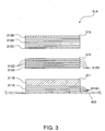
- Fig. 3 is a sectional view schematically showing an outline of a laser light source unit which configures a light source device.
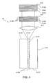
- Fig. 4 is a schematic diagram showing an outline of a configuration of a light source device 41 in a second embodiment.
- Fig. 1 is a sectional side view of a rear projector in a first embodiment according to the invention.
- the rear projector 1 is largely configured of a cabinet 2, a projector unit 3 as a projector, a control unit 4, a reflecting mirror 5 and a translucent screen 6.
- the cabinet 2 is configured as a box shape with a sloping back surface (a right side in Fig. 1), and contains the projector unit 3, the control unit 4 and the reflecting mirror 5 disposed in its interior.
- a power unit supplying power to each component member of the rear projector 1 and a cooling unit cooling the interior of the rear projector 1, a sound transmitter transmitting sound and the like are installed in the interior of the cabinet 2, as well as the projector unit 3, the control unit 4 and the reflecting mirror 5.
- a plan view rectangular aperture 21 is formed in a front surface of the cabinet 2 (a left side in Fig. 1), and the translucent screen 6 is secured to and supported by a surround of the aperture 21.
- the projector unit 3 being installed on a bottom surface in the cabinet 2, forms an image light L based on an image signal transmitted from the control unit 4, and projects it, enlarged, toward the reflecting mirror 5. A specific configuration of the projector unit 3 will be described hereafter.
- control unit 4 is configured to include, for example, a tuner, an interface circuit, a sound detecting circuit, an image detecting circuit, an amplifying circuit and a CPU etc., and carries out an overall control of the projector unit 3. Also, the control unit 4, for example, extracts a broadcast signal of a frequency corresponding to a channel selected in accordance with an operation of a remote controller (not shown) and, as well as transmitting an image signal to the projector unit 3, transmits a sound signal to the sound transmitter (not shown).
- the reflecting mirror 5 being installed on an upper inner portion of the back surface of the cabinet 2, reflects the image light L projected by the projector unit 3 onto a back surface of the translucent screen 6.
- the translucent screen 6 having a rectangular form, is secured to and supported by the surround of the aperture 21 of the cabinet 2.
- the translucent screen 6 is configured of a Fresnel lens sheet 61 installed on a back surface, and a lenticular lens sheet 62 installed on a front surface. Then, the translucent screen 6 converts the incident image light L via the reflecting mirror 5 into a parallel light with the Fresnel lens sheet 61, converts the parallel light into an enlarged (diffused) light with the lenticular lens sheet 62, projects the image light from the back surface to the front surface, and displays a projected image.
- Fig. 2 is a schematic diagram showing an outline of an optical system configured inside the projector unit.
- the projector unit 3 is configured of light source devices 31, liquid crystal panels 32, polarizing plates 33, a cross dichroic prism 34, a projection lens 35 and the like.
- An optical element according to an aspect of the invention is configured of the liquid crystal panels 32, the polarizing plates 33 and the cross dichroic prism 34.
- the light source devices 31 light up in accordance with a control signal received from the control unit, and emits laser beams toward the liquid crystal panels 32.
- the light source devices 31 include a red beam light source device 31R which emits a red laser beam, a blue beam light source device 31B which emits a blue laser beam, and a green beam light source device 31G which emits a green laser beam.
- the light source devices 31 are installed in such a way as to each face one of three sides of the cross dichroic prism 34.
- the light source devices 31 are installed in such a way that the red beam light source device 31R and the blue beam light source device 31B face each other, and the projection lens 35 and the green beam light source device 31G face each other, across the cross dichroic prism 34. A detailed description of the light source devices 31 will be given hereafter.
- each colored light emerging from the light source device 31 is modulated, in accordance with the image information, by the three liquid crystal panels 32 and the polarizing plates 33 on their luminous flux incidence side and emergence side, forming an optical image.
- a polysilicon TFT Thin Film Transistor
- the polarizing plates 33 each include incidence side polarizing plate 331 and emergence side polarizing plate 332 disposed on an optical path front line side and an optical path back line side of the liquid crystal panel 32.
- the incidence side polarizing plate 331 transmitting only polarized light of a certain direction from among the colored lights emerging from the light source device 31 and absorbing other luminous fluxes, has a polarizing film attached to a substrate of crystal, sapphire or the like.
- the emergence side polarizing plate 332 too, being configured in approximately the same way as the incidence side polarizing plate 331, transmits only polarized light of a prescribed direction from among the colored lights emerging from the liquid crystal panels 32 and absorbs other luminous fluxes.
- the incidence side polarizing plate 331 and the emergence side polarizing plate 332 are set in such a way that directions of their polarizing axis are mutually perpendicular.
- the cross dichroic prism 34 is an optical element which synthesizes the optical images polarized into each colored light emerging from each liquid crystal panel 32, forming a color image.
- the cross dichroic prism 34 is formed of four right-angle prisms attached together in a plan view approximately square form, with two dielectric multilayers formed on interfaces where the right-angle prisms adjoin.
- the dielectric multilayers reflect each colored light emerging from mutually opposing liquid crystal panels 32, and transmit colored light emerging from the liquid crystal panel 32 facing the projection lens 35. In this way, each colored light modulated by each liquid crystal panel 32 is synthesized, forming a color image.
- the projection lens 35 is configured as a combination lens having a plurality of lenses combined. Then, the projection lens 35 forms an image light L based on the color image formed by the cross dichroic prism 34, and projects it, enlarged, toward the reflecting mirror 5.
- Fig. 3 is a sectional view schematically showing an outline of a laser light source unit which configures the light source device.
- the light source device 31 is configured by disposing a plurality of laser light source units 31A in, for example, a series.
- the laser light source units 31A include a laser light source 311 which emits laser beams, a nonlinear optical element 312 which converts a wavelength of the laser beams emitted by the laser light source 311, and a VBG (Volume Bragg Grating) 313 as a volume phase grating which transmits laser beams of which the wavelength has been converted by the nonlinear optical element 312, and reflects laser beams of which the wavelength has not been converted.
- VBG Volume Bragg Grating
- the laser light source 311 is formed on a substrate 400, which is a semiconductor wafer, and includes a mirror layer 311A as a reflecting mirror, and a laser medium 311B which is stacked on a surface of the mirror layer 311A.
- the mirror layer 311A is formed directly on the substrate 400. That is, dielectric bodies are directly formed stacked in a layer form, by a method such as vapor deposition, at a wafer manufacturing stage of the substrate 400, and the mirror layer 311A is formed by the dielectric bodies. Also, the mirror layer 311A being formed of a high refractive index layer and a low refractive index layer stacked together, a thickness of each layer is set to a condition in which, from a wavelength of laser beams and a refractive index of each layer, reflected light interferes and mutually strengthens.
- the laser medium 311B is formed on an upper surface of the mirror layer 311A.
- the laser medium 311B being connected to a not-shown energizer, emits laser beams of a prescribed wavelength (hereafter, a wavelength of emitted laser beams will be referred to as an emission wavelength) on a prescribed volume of current flowing from the energizer.
- the laser medium 311B amplifies laser beams of a transmitted emission wavelength. That is, laser beams reflected by the mirror layer 311A and the VBG, to be described hereafter, are amplified resonating with laser beams newly emitted by the laser medium, and emerge in a direction approximately perpendicular to the substrate 400.
- the nonlinear optical element 312, facing the laser medium 311B of the laser light source 311, is disposed on an optical path of the laser beams emitted from the laser light source 311.
- the nonlinear optical element 312 is formed in a polarization reversal structure by alternately forming, at a prescribed interval, two areas 312B and 312C whose polarization directions are mutually reversed inside a crystalline substrate of an inorganic nonlinear optical material such as, for example, LN (LiNbO 3 ) or LT (LiTaO 3 ) .
- the prescribed interval is determined as appropriate by the wavelength of the laser beams emitted from the laser light source 311 and a refractive index dispersion of the nonlinear optical element.
- the nonlinear optical element 312 generates a second harmonic from the wavelength of the laser beams emitted from the laser light source 311 (hereafter, a wavelength converted by the nonlinear optical element 312 will be referred to as a converted wavelength). For example, it generates a green laser beam of a wavelength of 532nm from an infrared laser beam of an emission wavelength of 1064nm emitted from the laser light source 311.
- a luminosity of emergent laser beams of a converted wavelength is approximately proportional to the square of a luminosity of laser beams of an incident emission wavelength. For this reason, in order to improve a conversion efficiency, it is important to increase a luminosity of laser beams of an original emission wavelength.
- a second dielectric multilayer 312A is formed on a light incidence surface of the laser light source 311 side of the nonlinear optical element 312.
- the second dielectric multilayer 312A transmits laser beams of the emission wavelength at a transmittance of 95% or more, while reflecting laser beams of the converted wavelength at a reflectance of 95% or more.
- the VBG 313 is an element which band narrows and reflects the laser beams of the emission wavelength.
- the VBG 313 includes a Bragg layer 313A stacked along a laser beam optical path, a first dielectric multilayer 313B formed on an exterior end surface of the Bragg layer 313A on an opposite side to the nonlinear optical element 312, and a dielectric thin film 313C formed on an end surface of the Bragg layer 313A on the nonlinear optical element 312 side.
- the Bragg layer 313A projects an ultraviolet radiation of a prescribed wavelength onto a SiO 2 base glass layer of, for example, alkali boroaluminosilicate glass, forming interference patterns of differing refractive indexes in a layered formation inside the glass layer.
- laser beams of the emission wavelength only are selectively reflected, and an emission wavelength band of the laser beams is band narrowed. That is, in general, in a case of laser beams emitted from a laser diode, as a plurality of vertical modes is emitted in a gain band, their wavelengths change due to an effect of a fluctuation in temperature and the like.
- the wavelength band of the laser beams in general, is wider than an allowable wavelength band of a wavelength converted by the nonlinear optical element 312, a wavelength conversion efficiency in the nonlinear optical element 312 declines.
- the Bragg layer 313A of the VBG 312 reflects only laser beams of a specified wavelength, from among the laser beams emerging from the laser diode, and band narrows the emission wavelength of the laser beams. Meanwhile, the laser beams of the converted wavelength converted by the nonlinear optical element 312 pass through the Bragg layer 313A, and fall on the first dielectric multilayer 313B.
- the first dielectric multilayer 313B being a so-called dichroic filter, transmits the laser beams of the converted wavelength, and reflects laser beams of any other wavelength.
- the green beam light source device 31G it reflects the red laser beam, which is the laser beam of the emission wavelength, and transmits the green laser beam, which is of the converted wavelength.
- the first dielectric multilayer 313B reflects the laser beams of the emission wavelength at a reflectance of 95% or more, while transmitting the laser beams of the converted wavelength at a transmittance of 95% or more, and causes them to emerge from the light source device 31.
- the dielectric thin film 313C being formed by a single layer or multiple layers of an AR coating (anti-reflective coating), transmits both the laser beam of the emission wavelength and the laser beam of the converted wavelength at a transmittance of 98% or more.
- nonlinear optical element 312 and the VBG 313 are disposed on a surface approximately perpendicular to an optical axis of the laser beams emerging from the laser light source.
- the light source device 31 emits laser beams of a prescribed wavelength when a current is caused to flow through the laser medium 311B of the laser light source 311, by means of a control of the control unit 4.
- the green beam light source device 31G on a current being applied to the laser medium 311B, it emits, for example, an infrared laser beam of a wavelength of 1064nm.
- the laser beams emitted from among the laser beams emitted, it emits laser beams which proceed in a direction approximately perpendicular to the substrate 400 from an end surface of the laser medium 311B on the nonlinear optical element 312 side.
- laser beams which proceed on the substrate 400 side are also reflected by the second dielectric multilayer 312A, pass through the laser beam medium again, and emerge to the nonlinear optical element 312.
- the incident laser beams of the emission wavelength are wavelength converted by the nonlinear optical element 312.
- the nonlinear optical element 312 For example, in a case of the green beam light source device 31G, an infrared laser beam emitted by the laser light source 311 is wavelength converted to a green laser beam of a wavelength of 532nm.
- the laser beams which have passed through the nonlinear optical element 312 fall on the VBG 313.
- the Bragg layer 313A of the VBG 313 reflects only the laser beams, from among the incident laser beams, which have the set specified wavelength. For this reason, the emission wavelength of the laser beams, being unaffected by a fluctuation in temperature, is always constant, enabling a band narrowing of simultaneously emitted laser beams.
- the laser beams of the converted wavelength converted by the nonlinear optical element 312 pass through the Bragg layer 313A and the first dielectric multilayer 313B.
- the laser beams which have passed through the first dielectric multilayer 313B fall on the liquid crystal panels 32, the polarizing plate 33 and the cross dichroic prism 34, synthesized with other laser beams, and are projected from the projection lens 35 as the image light L.
- the laser beams of the emission wavelength reflected by the VBG 313 fall again on the nonlinear optical element 312, and are wavelength converted. At this time, as the wavelength of the reflected laser beams of the emission wavelength has been band narrowed, the conversion efficiency in the nonlinear optical element 312 improves.
- the thus wavelength converted laser beams, and the laser beams of the converted wavelength reflected by the VBG 313, are reflected by the second dielectric multilayer 312A, fall again on the VBG 313 side, and emerge from the first dielectric multilayer 313B.
- the laser beams of the converted wavelength do not proceed on a wasteful optical path, it is possible to suppress a laser beam output reduction.
- the laser beams of the emission wavelength which have not been wavelength converted by the nonlinear optical element 312 pass through the second dielectric multilayer 312A, and fall on the laser light source.
- the laser beams of the emission wavelength falling on the laser light source resonate with the laser beams newly emitted by the laser medium.
- the laser output of the laser beams is amplified, and they emerge again toward the nonlinear optical element 312.
- the laser beams of the emission wavelength are band narrowed by the VBG, and caused to come and go between the mirror layer 311A of the laser light source and the first dielectric multilayer 313B of the VBG 313. For this reason, the output of the laser beams is further amplified, thus enabling a further improvement in the wavelength conversion efficiency.
- Fig. 4 is a schematic diagram showing an outline of a configuration of a light source device 41 in the second embodiment.
- the light source device 41 in place of the light source device 31 contained inside the projector unit 3 in the first embodiment, the light source device 41, using a so-called end surface-emitting laser diode, is used.
- the light source device 41 in the second embodiment includes a longitudinal laser light source 411, a parallelizing lens 412, a nonlinear optical element 312 and a VBG 313.
- the laser light source 411 is a so-called end surface-emitting laser diode in which a longitudinal laser medium 411A is sandwiched between clad layers 411B.
- a mirror layer 411C being formed as a reflecting mirror on each longitudinal end surface of the laser medium 411A, by reflecting laser beams between the mirror layers 411C, an output of the laser beams is amplified.
- a not-shown energizer being provided to the laser medium 411A, on a prescribed volume of current being sent from the energizer by a control of the control unit 4, laser beams of a prescribed emitted wavelength are emitted.
- the mirror layers 411C being formed on both end surfaces of the laser medium 411A, as described heretofore, by reflecting the laser beams emitted by the laser medium 411A between the mirror layers 411C, the laser beams are caused to resonate and an output is amplified. Also, an emergence portion 411D is formed on one of the mirror layers 411C, facing the parallelizing lens 412 which acts as a beam parallelizer, and the emitted laser beams emerge from the emergence portion 411D.
- the parallelizing lens 412 converts the laser beams emerging from the emergence portion 411D of the laser light source 411 into parallel luminous fluxes.
- the nonlinear optical element 312 having the same configuration as the nonlinear optical element 312 in the first embodiment, is disposed facing the parallelizing lens 412.
- a second dielectric multilayer 312A is formed on an end surface of the nonlinear optical element 312, on the parallelizing lens 412 side.
- the light source device 41 emits laser beams of a prescribed wavelength when a current is caused to flow through the laser medium 411A of the laser light source 411, by means of a control of the control unit 4.
- the emitted laser beams are reflected by the mirror layers 411C on both end surfaces of the laser medium 411A, and come and go inside the laser medium 411A. Then, while coming and going inside the laser medium 411A, they resonate with newly emitted laser beams etc., and their output is amplified. Then, one portion of the amplified laser beams emerges from the emergence portion 411D to the parallelizing lens 412 side.
- the laser beams emerging from the emergence portion 411D are converted into parallel luminous fluxes by the parallelizing lens 412 and fall on the nonlinear optical element 312, whereon laser beams of an emission wavelength are wavelength converted by the nonlinear optical element 312.
- the laser beams which have passed through the nonlinear optical element 312 fall on the VBG 313.
- the Bragg layer 313A of the VBG 313 reflects only the laser beams, from among the incident laser beams, of the emission wavelength, band narrowing the laser beams of the emission wavelength.
- the laser beams of the converted wavelength converted by the nonlinear optical element 312 pass through a Bragg layer 313A and the first dielectric multilayer 313B, and emerge from the light source device 41.
- the laser beams of the emission wavelength reflected by the VBG 313 fall again on the nonlinear optical element 312, and are wavelength converted. Then, the thus wavelength converted laser beams, and one portion of the laser beams of the converted wavelength reflected by the VBG 313, are reflected by the second dielectric multilayer 312A, fall again on the VBG 313 side, and emerge from the first dielectric multilayer 313B. Meanwhile, the laser beams of the emission wavelength which have not been wavelength converted by the nonlinear optical element 312 pass through the second dielectric multilayer 312A, and emerge to the parallelizing lens 412 side.
- the luminous fluxes are converged toward the emergence portion 411D of the laser light source 411, and fall on the laser medium 411A from the emergence portion 411D.
- the laser beams of the emission wavelength falling on the laser light source 411 resonate with laser beams newly emitted by the laser medium 411A, and a laser output is amplified.
- the nonlinear optical element 312 is disposed between the laser light source 411 and the VBG 313, and the first dielectric multilayer 313B, which transmits the laser beams of the converted wavelength, is formed on the emergence side end surface of the VBG 313.
- the first dielectric multilayer 313B which transmits the laser beams of the converted wavelength
- the nonlinear optical element 312 and the VBG 313, using a so-called end surface-emitting laser diode which amplifies the output of the laser beams by reflecting the laser beams at the mirror layers 411C on both end surfaces of the longitudinal laser medium 411A, as the laser light source 411, and causes the amplified laser beams to emerge from the emergence portion 411D, are disposed beyond the parallelizing lens 412 which converts the laser beams into parallel beams.
- laser beams which have not been wavelength converted by the nonlinear optical element 312 are band narrowed and reflected by the VBG 313, pass through the parallelizing lens 412 and fall again from the emergence portion 411D on the laser medium 411A, enabling an amplification of the laser beam output. Consequently, even in the case of the end surface-emitting laser diode, it is possible to improve an emission efficiency.
- the red beam light source device 31R, the blue beam light source device 31B and the green beam light source device 31G each include the laser light source 311, the nonlinear optical element 312 and the VBG 313, as shown in Fig. 3, but the invention is not limited to this. That is, in a case of a red laser beam and a blue laser beam, it is possible to cause the red laser beam and the blue laser beam to be emitted directly from the laser light source 311, by selecting an appropriate article as the semiconductor laser element which is the laser medium.
- a configuration of the second dielectric multilayer 312A is such that it transmits the laser beams of the emission wavelength while reflecting the laser beams of the converted wavelength, but it is also acceptable that it transmits both.
- the nonlinear optical material configuring the nonlinear optical element 312 is exemplified by LN (LiNbO 3 ) and LT (LiTaO 3 ), but it is also acceptable to use an inorganic nonlinear optical material other than these, such as KNbO 3 , BNN (Ba 2 NaNb 5 O 15 ), KTP (KTiOPO 4 ), KTA (KTiOAsO 4 ), BBO ( ⁇ -BaB 2 O 4 ) or LBO (LiB 3 O 7 ).
- a low molecular organic material such as metanitroaniline, 2-methyl-4-nitroaniline, chalcone, dicyanovinylanisole, 3,5-dimethyl-1-(4-nitrophenyl) pyrazole, or N-methoxymethyl-4-nitroaniline, or an organic nonlinear optical element such as a poled polymer.
- the nonlinear optical element 312 and the VBG 313 are commonly used by a plurality of laser elements, without being limited to this, it is also acceptable to configure in such a way that each laser element is provided with one each.
- the light source units 31 and 41 configuring the projector unit 3 loaded on the rear projector 1 are shown as examples but, without being limited to this, they can also be used in another type of projector, such as a front projector.
- a front projector For example, apart from a transmissive liquid crystal light valve or a reflective liquid crystal light valve, it is also acceptable to employ a digital micromirror device (Texas Instruments brand name).
- the invention can be used in a light source device which emits a laser beam, and a projector which includes the light source device.
Landscapes
- Physics & Mathematics (AREA)
- Optics & Photonics (AREA)
- General Physics & Mathematics (AREA)
- Electromagnetism (AREA)
- Engineering & Computer Science (AREA)
- Condensed Matter Physics & Semiconductors (AREA)
- Multimedia (AREA)
- Signal Processing (AREA)
- Plasma & Fusion (AREA)
- Optical Modulation, Optical Deflection, Nonlinear Optics, Optical Demodulation, Optical Logic Elements (AREA)
- Semiconductor Lasers (AREA)
Abstract
Description
- The present invention relates to a light source device which emits a laser beam, and a projector including the light source device
- To date, a laser diode has been known which loads a prescribed amount of energy on a laser medium, reflects laser beams emerging from the laser medium with mirrors provided at both ends of the laser medium, and amplifies an output of the laser beams at the laser medium. (For example, refer to
JP-A-6-132595 Pages 2 to 3 and Figs. 1 and 2)). - A laser diode disclosed in
JP-A-6-132595 - However, in a case of a heretofore known second harmonic light generator such as that disclosed in
JP-A-6-132595 - An advantage of some aspects of the invention is to provide a light source device which effectively emits a laser beam, and a projector including the light source device.
- A light source device according to one aspect of the invention includes: a laser light source emitting a laser beam of a prescribed wavelength; a nonlinear optical element, disposed facing a light emergence surface of the laser light source, which converts an emission wavelength of the laser beam emitted from the laser light source and causes the laser beam to emerge; a volume phase grating, disposed facing an emergence surface of the laser beam of the converted wavelength converted by the nonlinear optical element, which has formed in an interior thereof a Bragg grating structure which selectively reflects a laser beam of an emission wavelength; and a first dielectric multilayer, provided on a light emergence surface of the volume phase grating, which transmits the laser beam of the converted wavelength and reflects the laser beam of the emission wavelength.
- In this case, it is preferable that the Bragg grating of the volume phase grating reflects the laser beams at a reflectance of 95% or more with respect to the laser beams of the emission wavelength, while the first dielectric multilayer transmits the laser beams at a reflectance of 5% or less with respect to the wavelength converted laser beams.
- In this kind of aspect of the invention, the nonlinear optical unit is disposed between the laser light source and the volume phase grating, and the laser beam emission wavelength is band narrowed by the Bragg grating of the volume phase grating. By this means, even in the event, for example, that a discrepancy occurs in the laser beam emission wavelength due to a fluctuation in temperature and the like, and a wavelength band of the emitted laser beams is widened, the laser beams of the emission wavelength are band narrowed by the Bragg grating of the volume phase grating. Consequently, even in the event of a discrepancy occurring in an emission wavelength of a laser diode due to a fluctuation in temperature and the like, and a wavelength band widening, it is possible to band narrow and standardize the laser beam emission wavelength by the volume phase grating. Therefore, a conversion efficiency of a wavelength conversion of the laser beams of the emission wavelength by the nonlinear optical element improves.
- Also, as the nonlinear optical element is interposed between the laser light source and the volume phase grating, it is possible to effectively convert the wavelength of the laser beams of the emission wavelength coming and going between them, meaning that the wavelength conversion efficiency of the laser beams improves. Furthermore, by reflecting an increased number of the laser beams of the emission wavelength by the first dielectric multilayer of the volume phase grating, a resonance of the laser light source by the laser medium of the laser light source is promoted, and a laser beam output is amplified. Therefore, the laser beam emission efficiency and the wavelength conversion efficiency further improve, making it possible to project an effective laser beam from the light source device.
- In one aspect of the invention, it is preferable to include a dielectric thin film, provided on a light incidence surface of the volume phase grating, which suppresses a reflection of the laser beam of the emission wavelength and the laser beam of the converted wavelength to the nonlinear optical element side.
- According to this aspect of the invention, a dielectric thin film suppressing a reflection of both the laser beams of the emission wavelength and the laser beams of the converted wavelength is formed on the light incidence surface of the volume phase grating. By this means, it is possible to effectively cause the laser beams of the converted wavelength to fall on the volume phase grating, and it is possible to effectively cause the laser beams of the emission wavelength reflected by the volume phase grating to emerge to the nonlinear optical element side.
- In one aspect of the invention, it is preferable that the nonlinear optical element, being a bulk nonlinear optical element having a polarization reversal structure, includes: a second dielectric multilayer, provided on the light incidence surface of the nonlinear optical element, which reflects the laser beam of the converted wavelength and transmits the laser beam of the emission wavelength.
- In this case, it is preferable that a second dielectric multiplayer reflectance with respect to the laser beams of the converted wavelength is 95% or more, while a reflectance with respect to the laser beams of the emission wavelength is 5% or less.
- According to this aspect of the invention, the second dielectric multilayer which reflects the laser beams of the converted wavelength, and transmits the laser beams of the emission wavelength, is formed on the light incidence surface of the nonlinear optical element. By this means, the laser beams of the emission wavelength pass through the dielectric multilayer, whereon the laser beams of the emission wavelength transmitted and laser beams newly emitted by the laser light source resonate. Consequently, the output of the laser beams is amplified by the resonance of the laser beams, making it possible to improve the emission efficiency. Meanwhile, the laser beams of the converted wavelength are reflected by the second dielectric multiplayer, and emerge from the first dielectric multiplayer of the volume phase grating. Consequently, as the laser beams of the converted wavelength emerge from the first dielectric multiplayer without proceeding on a wasteful optical path, it is possible to suppress a laser beam energy loss, enabling an improvement in an emission output of the light source device.
- In one aspect of the invention, it is preferable that the laser light source is a surface-emitting laser diode, including a reflecting mirror formed on a semiconductor wafer and a laser medium formed stacked on the reflecting mirror, which emits a laser beam and transmits it in a stacking direction of the reflecting mirror and the laser medium.
- In the case of the surface-emitting laser diode, as it is possible to form a plurality of laser elements on the same semiconductor wafer, laser beams emitted from each of the laser elements emerge approximately vertically to a semiconductor wafer surface, in a mutually parallel direction. Consequently, it is possible to cause the emitted beams emerging from each of the laser elements to fall on the nonlinear optical element and the volume phase grating, and subject each of them to wavelength conversion and reflection of the emitted beams. By adopting this kind of configuration, it is possible for the laser elements of the plurality of surface-emitting laser diodes to share a use of the nonlinear optical element and the volume phase grating. By forming a plurality of laser elements in close proximity, even while increasing a power of the emergent laser beams by that number, it is possible and preferable to adopt an extremely compact configuration.
- Meanwhile, it is also acceptable to have a configuration in which, the laser light source is a surface-emitting laser diode including a laser medium sandwiched between clad layers, and a pair of reflecting mirrors disposed facing both ends of the laser medium, wherein a beam parallelizer which parallelizes the laser beam emitted from the laser light source is provided between the light emergence surface of the laser light source and the nonlinear optical element.
- According to this aspect of the invention, the laser light source being a so-called end surface-emitting laser diode which reflects the laser beams with an end surface of a laser medium sandwiched between clad layers, amplifies the output of the laser beams, and causes them to emerge, the nonlinear optical element and volume phase grating are disposed beyond the beam parallelizer which converts the laser beams into parallel beams. By this means, the laser beams which have not been wavelength converted by the nonlinear optical element are reflected by the volume phase grating, pass through the parallelizing lens, and emerge again from an emergence portion to the laser medium, enabling an amplification of the laser beam output.
- It is preferable that a projector according to one aspect of the invention includes: a light source device emitting a laser beam; an optical modulator which modulates the laser beam emitted from the light source device in accordance with image information; and a projection optical system which projects the modulated laser beam, wherein the light source device is a light source device such as that described heretofore.
- According to this aspect of the invention, in the projector, as the laser beams efficiently wavelength converted by the kind of light source device heretofore described are caused to emerge without causing any reduction in the emission output, it is possible to prevent any increase etc. in power consumed due to an energy loss. Also, it is possible to provide the laser light source with a projector of a simpler configuration, and which can be miniaturized.
- The invention will be described with reference to the accompanying drawings, wherein like numbers reference like elements.
- Fig. 1 is a sectional side view of a rear projector in a first embodiment according to the invention.
- Fig. 2 is a schematic diagram showing an outline of an optical system configured inside a projector unit.
- Fig. 3 is a sectional view schematically showing an outline of a laser light source unit which configures a light source device.
- Fig. 4 is a schematic diagram showing an outline of a configuration of a
light source device 41 in a second embodiment. - Hereafter, a description will be given of an embodiment of the invention, based on the drawings. Main configuration of a rear projector
- Fig. 1 is a sectional side view of a rear projector in a first embodiment according to the invention. In Fig. 1, 1 being a rear projector, the
rear projector 1 is largely configured of acabinet 2, aprojector unit 3 as a projector, acontrol unit 4, a reflectingmirror 5 and atranslucent screen 6. - As shown in Fig. 1, the
cabinet 2 is configured as a box shape with a sloping back surface (a right side in Fig. 1), and contains theprojector unit 3, thecontrol unit 4 and the reflectingmirror 5 disposed in its interior. Although a specific depiction is omitted, a power unit supplying power to each component member of therear projector 1, and a cooling unit cooling the interior of therear projector 1, a sound transmitter transmitting sound and the like are installed in the interior of thecabinet 2, as well as theprojector unit 3, thecontrol unit 4 and the reflectingmirror 5. - Also, a plan view
rectangular aperture 21 is formed in a front surface of the cabinet 2 (a left side in Fig. 1), and thetranslucent screen 6 is secured to and supported by a surround of theaperture 21. - The
projector unit 3, being installed on a bottom surface in thecabinet 2, forms an image light L based on an image signal transmitted from thecontrol unit 4, and projects it, enlarged, toward the reflectingmirror 5. A specific configuration of theprojector unit 3 will be described hereafter. - Although a specific depiction is omitted, the
control unit 4 is configured to include, for example, a tuner, an interface circuit, a sound detecting circuit, an image detecting circuit, an amplifying circuit and a CPU etc., and carries out an overall control of theprojector unit 3. Also, thecontrol unit 4, for example, extracts a broadcast signal of a frequency corresponding to a channel selected in accordance with an operation of a remote controller (not shown) and, as well as transmitting an image signal to theprojector unit 3, transmits a sound signal to the sound transmitter (not shown). - The reflecting
mirror 5, being installed on an upper inner portion of the back surface of thecabinet 2, reflects the image light L projected by theprojector unit 3 onto a back surface of thetranslucent screen 6. - The
translucent screen 6, having a rectangular form, is secured to and supported by the surround of theaperture 21 of thecabinet 2. Thetranslucent screen 6 is configured of a Fresnellens sheet 61 installed on a back surface, and alenticular lens sheet 62 installed on a front surface. Then, thetranslucent screen 6 converts the incident image light L via the reflectingmirror 5 into a parallel light with theFresnel lens sheet 61, converts the parallel light into an enlarged (diffused) light with thelenticular lens sheet 62, projects the image light from the back surface to the front surface, and displays a projected image. - Next, a description will be given of a configuration of the
projector unit 3, based on Fig. 2. Fig. 2 is a schematic diagram showing an outline of an optical system configured inside the projector unit. - The
projector unit 3 is configured of light source devices 31,liquid crystal panels 32,polarizing plates 33, a crossdichroic prism 34, aprojection lens 35 and the like. An optical element according to an aspect of the invention is configured of theliquid crystal panels 32, thepolarizing plates 33 and the crossdichroic prism 34. - The light source devices 31 light up in accordance with a control signal received from the control unit, and emits laser beams toward the
liquid crystal panels 32. The light source devices 31 include a red beam light source device 31R which emits a red laser beam, a blue beam light source device 31B which emits a blue laser beam, and a green beam light source device 31G which emits a green laser beam. As shown in Fig. 2, the light source devices 31 are installed in such a way as to each face one of three sides of the crossdichroic prism 34. Herein, the light source devices 31 are installed in such a way that the red beam light source device 31R and the blue beam light source device 31B face each other, and theprojection lens 35 and the green beam light source device 31G face each other, across the crossdichroic prism 34. A detailed description of the light source devices 31 will be given hereafter. - The
liquid crystal panels 32 using, for example, a polysilicon TFT (Thin Film Transistor) as a switching element, each colored light emerging from the light source device 31 is modulated, in accordance with the image information, by the threeliquid crystal panels 32 and thepolarizing plates 33 on their luminous flux incidence side and emergence side, forming an optical image. - The
polarizing plates 33 each include incidence sidepolarizing plate 331 and emergenceside polarizing plate 332 disposed on an optical path front line side and an optical path back line side of theliquid crystal panel 32. The incidence sidepolarizing plate 331, transmitting only polarized light of a certain direction from among the colored lights emerging from the light source device 31 and absorbing other luminous fluxes, has a polarizing film attached to a substrate of crystal, sapphire or the like. The emergenceside polarizing plate 332 too, being configured in approximately the same way as the incidence sidepolarizing plate 331, transmits only polarized light of a prescribed direction from among the colored lights emerging from theliquid crystal panels 32 and absorbs other luminous fluxes. Also, it is acceptable to attach the polarizing film to the crossdichroic prism 34, without using the substrate, or to attach the substrate to the crossdichroic prism 34. The incidence sidepolarizing plate 331 and the emergenceside polarizing plate 332 are set in such a way that directions of their polarizing axis are mutually perpendicular. - The cross
dichroic prism 34 is an optical element which synthesizes the optical images polarized into each colored light emerging from eachliquid crystal panel 32, forming a color image. The crossdichroic prism 34 is formed of four right-angle prisms attached together in a plan view approximately square form, with two dielectric multilayers formed on interfaces where the right-angle prisms adjoin. The dielectric multilayers reflect each colored light emerging from mutually opposingliquid crystal panels 32, and transmit colored light emerging from theliquid crystal panel 32 facing theprojection lens 35. In this way, each colored light modulated by eachliquid crystal panel 32 is synthesized, forming a color image. - The
projection lens 35 is configured as a combination lens having a plurality of lenses combined. Then, theprojection lens 35 forms an image light L based on the color image formed by the crossdichroic prism 34, and projects it, enlarged, toward the reflectingmirror 5. - Next, a description will be given of a configuration of the light source device 31. Fig. 3 is a sectional view schematically showing an outline of a laser light source unit which configures the light source device.
- Herein, the light source device 31 is configured by disposing a plurality of laser
light source units 31A in, for example, a series. As shown in Fig. 3, the laserlight source units 31A include alaser light source 311 which emits laser beams, a nonlinearoptical element 312 which converts a wavelength of the laser beams emitted by thelaser light source 311, and a VBG (Volume Bragg Grating) 313 as a volume phase grating which transmits laser beams of which the wavelength has been converted by the nonlinearoptical element 312, and reflects laser beams of which the wavelength has not been converted. - As shown in Fig. 3, the
laser light source 311 is formed on asubstrate 400, which is a semiconductor wafer, and includes amirror layer 311A as a reflecting mirror, and alaser medium 311B which is stacked on a surface of themirror layer 311A. - The
mirror layer 311A is formed directly on thesubstrate 400. That is, dielectric bodies are directly formed stacked in a layer form, by a method such as vapor deposition, at a wafer manufacturing stage of thesubstrate 400, and themirror layer 311A is formed by the dielectric bodies. Also, themirror layer 311A being formed of a high refractive index layer and a low refractive index layer stacked together, a thickness of each layer is set to a condition in which, from a wavelength of laser beams and a refractive index of each layer, reflected light interferes and mutually strengthens. - The
laser medium 311B is formed on an upper surface of themirror layer 311A. Thelaser medium 311B, being connected to a not-shown energizer, emits laser beams of a prescribed wavelength (hereafter, a wavelength of emitted laser beams will be referred to as an emission wavelength) on a prescribed volume of current flowing from the energizer. Also, thelaser medium 311B amplifies laser beams of a transmitted emission wavelength. That is, laser beams reflected by themirror layer 311A and the VBG, to be described hereafter, are amplified resonating with laser beams newly emitted by the laser medium, and emerge in a direction approximately perpendicular to thesubstrate 400. - The nonlinear
optical element 312, facing thelaser medium 311B of thelaser light source 311, is disposed on an optical path of the laser beams emitted from thelaser light source 311. The nonlinearoptical element 312 is formed in a polarization reversal structure by alternately forming, at a prescribed interval, twoareas laser light source 311 and a refractive index dispersion of the nonlinear optical element. The nonlinearoptical element 312 generates a second harmonic from the wavelength of the laser beams emitted from the laser light source 311 (hereafter, a wavelength converted by the nonlinearoptical element 312 will be referred to as a converted wavelength). For example, it generates a green laser beam of a wavelength of 532nm from an infrared laser beam of an emission wavelength of 1064nm emitted from thelaser light source 311. - Furthermore, in the nonlinear
optical element 312, a luminosity of emergent laser beams of a converted wavelength is approximately proportional to the square of a luminosity of laser beams of an incident emission wavelength. For this reason, in order to improve a conversion efficiency, it is important to increase a luminosity of laser beams of an original emission wavelength. - Then, a
second dielectric multilayer 312A is formed on a light incidence surface of thelaser light source 311 side of the nonlinearoptical element 312. Thesecond dielectric multilayer 312A transmits laser beams of the emission wavelength at a transmittance of 95% or more, while reflecting laser beams of the converted wavelength at a reflectance of 95% or more. - The
VBG 313 is an element which band narrows and reflects the laser beams of the emission wavelength. TheVBG 313 includes aBragg layer 313A stacked along a laser beam optical path, afirst dielectric multilayer 313B formed on an exterior end surface of theBragg layer 313A on an opposite side to the nonlinearoptical element 312, and a dielectricthin film 313C formed on an end surface of theBragg layer 313A on the nonlinearoptical element 312 side. - The
Bragg layer 313A projects an ultraviolet radiation of a prescribed wavelength onto a SiO2 base glass layer of, for example, alkali boroaluminosilicate glass, forming interference patterns of differing refractive indexes in a layered formation inside the glass layer. In theBragg layer 313A, laser beams of the emission wavelength only are selectively reflected, and an emission wavelength band of the laser beams is band narrowed. That is, in general, in a case of laser beams emitted from a laser diode, as a plurality of vertical modes is emitted in a gain band, their wavelengths change due to an effect of a fluctuation in temperature and the like. In this way, as the wavelength band of the laser beams, in general, is wider than an allowable wavelength band of a wavelength converted by the nonlinearoptical element 312, a wavelength conversion efficiency in the nonlinearoptical element 312 declines. In response to this, theBragg layer 313A of theVBG 312 reflects only laser beams of a specified wavelength, from among the laser beams emerging from the laser diode, and band narrows the emission wavelength of the laser beams. Meanwhile, the laser beams of the converted wavelength converted by the nonlinearoptical element 312 pass through theBragg layer 313A, and fall on thefirst dielectric multilayer 313B. - The
first dielectric multilayer 313B, being a so-called dichroic filter, transmits the laser beams of the converted wavelength, and reflects laser beams of any other wavelength. For example, in a case of the green beam light source device 31G, it reflects the red laser beam, which is the laser beam of the emission wavelength, and transmits the green laser beam, which is of the converted wavelength. At this time, thefirst dielectric multilayer 313B reflects the laser beams of the emission wavelength at a reflectance of 95% or more, while transmitting the laser beams of the converted wavelength at a transmittance of 95% or more, and causes them to emerge from the light source device 31. - The dielectric
thin film 313C, being formed by a single layer or multiple layers of an AR coating (anti-reflective coating), transmits both the laser beam of the emission wavelength and the laser beam of the converted wavelength at a transmittance of 98% or more. - Also, the nonlinear
optical element 312 and theVBG 313 are disposed on a surface approximately perpendicular to an optical axis of the laser beams emerging from the laser light source. - Next, an operation and an application of the light source device 31 of the
projector unit 3 of therear projector 1 in the embodiment will be described. - The light source device 31 emits laser beams of a prescribed wavelength when a current is caused to flow through the
laser medium 311B of thelaser light source 311, by means of a control of thecontrol unit 4. For example, in a case of the green beam light source device 31G, on a current being applied to thelaser medium 311B, it emits, for example, an infrared laser beam of a wavelength of 1064nm. Herein, from among the laser beams emitted, it emits laser beams which proceed in a direction approximately perpendicular to thesubstrate 400 from an end surface of thelaser medium 311B on the nonlinearoptical element 312 side. Also, laser beams which proceed on thesubstrate 400 side are also reflected by thesecond dielectric multilayer 312A, pass through the laser beam medium again, and emerge to the nonlinearoptical element 312. - Then, the incident laser beams of the emission wavelength are wavelength converted by the nonlinear
optical element 312. For example, in a case of the green beam light source device 31G, an infrared laser beam emitted by thelaser light source 311 is wavelength converted to a green laser beam of a wavelength of 532nm. - Subsequently, the laser beams which have passed through the nonlinear
optical element 312 fall on theVBG 313. Then, theBragg layer 313A of theVBG 313 reflects only the laser beams, from among the incident laser beams, which have the set specified wavelength. For this reason, the emission wavelength of the laser beams, being unaffected by a fluctuation in temperature, is always constant, enabling a band narrowing of simultaneously emitted laser beams. - Meanwhile, the laser beams of the converted wavelength converted by the nonlinear
optical element 312 pass through theBragg layer 313A and thefirst dielectric multilayer 313B. The laser beams which have passed through thefirst dielectric multilayer 313B fall on theliquid crystal panels 32, thepolarizing plate 33 and the crossdichroic prism 34, synthesized with other laser beams, and are projected from theprojection lens 35 as the image light L. - Also, the laser beams of the emission wavelength reflected by the
VBG 313 fall again on the nonlinearoptical element 312, and are wavelength converted. At this time, as the wavelength of the reflected laser beams of the emission wavelength has been band narrowed, the conversion efficiency in the nonlinearoptical element 312 improves. - Then, the thus wavelength converted laser beams, and the laser beams of the converted wavelength reflected by the
VBG 313, are reflected by thesecond dielectric multilayer 312A, fall again on theVBG 313 side, and emerge from thefirst dielectric multilayer 313B. As such, as the laser beams of the converted wavelength do not proceed on a wasteful optical path, it is possible to suppress a laser beam output reduction. Also, the laser beams of the emission wavelength which have not been wavelength converted by the nonlinearoptical element 312 pass through thesecond dielectric multilayer 312A, and fall on the laser light source. - Then, the laser beams of the emission wavelength falling on the laser light source resonate with the laser beams newly emitted by the laser medium. By this means, the laser output of the laser beams is amplified, and they emerge again toward the nonlinear
optical element 312. - As described heretofore, in the light source device 31, the laser beams of the emission wavelength are band narrowed by the VBG, and caused to come and go between the
mirror layer 311A of the laser light source and thefirst dielectric multilayer 313B of theVBG 313. For this reason, the output of the laser beams is further amplified, thus enabling a further improvement in the wavelength conversion efficiency. - Also, when using a surface-emitting laser diode, it being possible to form a plurality of laser elements in close proximity in the
substrate 400 of the same semiconductor wafer, at this time, the emergent laser beams emerge parallel to each other. For this reason, it is possible to share the use of the same nonlinearoptical element 312 andVBG 313. By integrating a plurality of laser elements in this way, it is possible to increase the output of the transmitted laser beams by the number of the laser elements, without enlarging the light source device 31. - Next, a description will be given of a second embodiment of the invention, based on the drawings. In the following description, identical reference numerals are appended to structures and members identical to those in the first embodiment, and a detailed description is omitted or simplified. Fig. 4 is a schematic diagram showing an outline of a configuration of a
light source device 41 in the second embodiment. - In the second embodiment, in place of the light source device 31 contained inside the
projector unit 3 in the first embodiment, thelight source device 41, using a so-called end surface-emitting laser diode, is used. - As shown in Fig. 4, the
light source device 41 in the second embodiment includes a longitudinallaser light source 411, a parallelizinglens 412, a nonlinearoptical element 312 and aVBG 313. - The
laser light source 411 is a so-called end surface-emitting laser diode in which alongitudinal laser medium 411A is sandwiched betweenclad layers 411B. Amirror layer 411C being formed as a reflecting mirror on each longitudinal end surface of thelaser medium 411A, by reflecting laser beams between the mirror layers 411C, an output of the laser beams is amplified. A not-shown energizer being provided to thelaser medium 411A, on a prescribed volume of current being sent from the energizer by a control of thecontrol unit 4, laser beams of a prescribed emitted wavelength are emitted. - The mirror layers 411C being formed on both end surfaces of the
laser medium 411A, as described heretofore, by reflecting the laser beams emitted by thelaser medium 411A between the mirror layers 411C, the laser beams are caused to resonate and an output is amplified. Also, anemergence portion 411D is formed on one of the mirror layers 411C, facing the parallelizinglens 412 which acts as a beam parallelizer, and the emitted laser beams emerge from theemergence portion 411D. - The parallelizing
lens 412 converts the laser beams emerging from theemergence portion 411D of thelaser light source 411 into parallel luminous fluxes. - The nonlinear
optical element 312, having the same configuration as the nonlinearoptical element 312 in the first embodiment, is disposed facing the parallelizinglens 412. Asecond dielectric multilayer 312A is formed on an end surface of the nonlinearoptical element 312, on the parallelizinglens 412 side. - The
VBG 313, having the same configuration as theVBG 313 in the first embodiment, is disposed facing the nonlinearoptical element 312. Then, afirst dielectric multilayer 313B is formed on an emergence side end surface of theVBG 313, while a dielectricthin film 313C is formed on an incidence side end surface. - Next, an operation of the
light source device 41 in the second embodiment will be described. - The
light source device 41 emits laser beams of a prescribed wavelength when a current is caused to flow through thelaser medium 411A of thelaser light source 411, by means of a control of thecontrol unit 4. Herein, the emitted laser beams are reflected by the mirror layers 411C on both end surfaces of thelaser medium 411A, and come and go inside thelaser medium 411A. Then, while coming and going inside thelaser medium 411A, they resonate with newly emitted laser beams etc., and their output is amplified. Then, one portion of the amplified laser beams emerges from theemergence portion 411D to the parallelizinglens 412 side. - Then, the laser beams emerging from the
emergence portion 411D are converted into parallel luminous fluxes by the parallelizinglens 412 and fall on the nonlinearoptical element 312, whereon laser beams of an emission wavelength are wavelength converted by the nonlinearoptical element 312. - Subsequently, the laser beams which have passed through the nonlinear
optical element 312 fall on theVBG 313. Then, theBragg layer 313A of theVBG 313 reflects only the laser beams, from among the incident laser beams, of the emission wavelength, band narrowing the laser beams of the emission wavelength. Meanwhile, the laser beams of the converted wavelength converted by the nonlinearoptical element 312 pass through aBragg layer 313A and thefirst dielectric multilayer 313B, and emerge from thelight source device 41. - Also, the laser beams of the emission wavelength reflected by the
VBG 313 fall again on the nonlinearoptical element 312, and are wavelength converted. Then, the thus wavelength converted laser beams, and one portion of the laser beams of the converted wavelength reflected by theVBG 313, are reflected by thesecond dielectric multilayer 312A, fall again on theVBG 313 side, and emerge from thefirst dielectric multilayer 313B. Meanwhile, the laser beams of the emission wavelength which have not been wavelength converted by the nonlinearoptical element 312 pass through thesecond dielectric multilayer 312A, and emerge to the parallelizinglens 412 side. Then, in a case of the laser beams emerging from thesecond dielectric multilayer 312A to thelaser light source 411 side, the luminous fluxes are converged toward theemergence portion 411D of thelaser light source 411, and fall on thelaser medium 411A from theemergence portion 411D. - Then, the laser beams of the emission wavelength falling on the
laser light source 411 resonate with laser beams newly emitted by thelaser medium 411A, and a laser output is amplified. - In the kind of
light source device 41 in the second embodiment, in the same way as the light source device 31 in the first embodiment, the nonlinearoptical element 312 is disposed between thelaser light source 411 and theVBG 313, and thefirst dielectric multilayer 313B, which transmits the laser beams of the converted wavelength, is formed on the emergence side end surface of theVBG 313. For this reason, in the same way as in the first embodiment, even in the event that a deviation occurs in the laser beam emission wavelength due to a fluctuation in temperature and the like, it is possible to band narrow the laser beams of the emission wavelength in theBragg layer 313A of theVBG 313, thereby enabling an improvement in a wavelength conversion efficiency of the laser beams of the emission wavelength by the nonlinearoptical element 312. - Also, the nonlinear
optical element 312 and theVBG 313, using a so-called end surface-emitting laser diode which amplifies the output of the laser beams by reflecting the laser beams at the mirror layers 411C on both end surfaces of thelongitudinal laser medium 411A, as thelaser light source 411, and causes the amplified laser beams to emerge from theemergence portion 411D, are disposed beyond the parallelizinglens 412 which converts the laser beams into parallel beams. For this reason, laser beams which have not been wavelength converted by the nonlinearoptical element 312 are band narrowed and reflected by theVBG 313, pass through the parallelizinglens 412 and fall again from theemergence portion 411D on thelaser medium 411A, enabling an amplification of the laser beam output. Consequently, even in the case of the end surface-emitting laser diode, it is possible to improve an emission efficiency. - The invention is not limited to the embodiments described heretofore, as modifications, improvements and the like within a scope enabling an achievement of the aim of the invention are included in the invention.
- For example, in the first and second embodiments, a configuration is shown in which the red beam light source device 31R, the blue beam light source device 31B and the green beam light source device 31G each include the
laser light source 311, the nonlinearoptical element 312 and theVBG 313, as shown in Fig. 3, but the invention is not limited to this. That is, in a case of a red laser beam and a blue laser beam, it is possible to cause the red laser beam and the blue laser beam to be emitted directly from thelaser light source 311, by selecting an appropriate article as the semiconductor laser element which is the laser medium. Consequently, it is also acceptable to configure in such a way that a heretofore known surface light emitting or an end surface-emitting laser diode is used for the red beam light source device 31R and the blue beam light source device 31B, while the kind of light source device 31 shown in Fig. 3 is used for only the green beam light source device 31G. - Furthermore, a configuration of the
second dielectric multilayer 312A is such that it transmits the laser beams of the emission wavelength while reflecting the laser beams of the converted wavelength, but it is also acceptable that it transmits both. - Also, in the embodiments, the nonlinear optical material configuring the nonlinear
optical element 312 is exemplified by LN (LiNbO3) and LT (LiTaO3), but it is also acceptable to use an inorganic nonlinear optical material other than these, such as KNbO3, BNN (Ba2NaNb5O15), KTP (KTiOPO4), KTA (KTiOAsO4), BBO (β-BaB2O4) or LBO (LiB3O7). Also, it is also acceptable to use a low molecular organic material such as metanitroaniline, 2-methyl-4-nitroaniline, chalcone, dicyanovinylanisole, 3,5-dimethyl-1-(4-nitrophenyl) pyrazole, or N-methoxymethyl-4-nitroaniline, or an organic nonlinear optical element such as a poled polymer. - Furthermore, in the embodiments, an example is shown in which the nonlinear
optical element 312 and theVBG 313 are commonly used by a plurality of laser elements, without being limited to this, it is also acceptable to configure in such a way that each laser element is provided with one each. - Then, in the first and second embodiments, the
light source units 31 and 41 configuring theprojector unit 3 loaded on therear projector 1 are shown as examples but, without being limited to this, they can also be used in another type of projector, such as a front projector. For example, apart from a transmissive liquid crystal light valve or a reflective liquid crystal light valve, it is also acceptable to employ a digital micromirror device (Texas Instruments brand name). - Although a best configuration etc. for implementing the invention are disclosed in the above description, the invention is by no means limited to this. That is, although the invention is especially depicted and described mainly with regard to specified embodiments, it is possible for those skilled in the art to add various modifications in form, material, quantity and other detailed configurations, with respect to the embodiments, without departing from the technical idea and scope of aim of the invention.
- Consequently, as the description limiting the forms, materials and the like disclosed above, being illustrative for the purpose of making it easier to understand the invention, does not limit the invention, descriptions using member names removing one part of the limitation or a whole of the limitation of the forms, materials and the like are included in the invention.
- The invention can be used in a light source device which emits a laser beam, and a projector which includes the light source device.
Claims (6)
- A light source device comprising:a laser light source emitting a laser beam of a prescribed wavelength;a nonlinear optical element, disposed facing a light emergence surface of the laser light source, which converts an emission wavelength of the laser beam emitted from the laser light source and causes the laser beam to emerge;a volume phase grating, disposed facing an emergence surface of the laser beam of the converted wavelength converted by the nonlinear optical element, which has formed in an interior thereof a Bragg grating structure which selectively reflects a laser beam of an emission wavelength; anda first dielectric multilayer, provided on a light emergence surface of the volume phase grating, which transmits the laser beam of the converted wavelength and reflects the laser beam of the emission wavelength.
- A light source device according to claim 1, comprising:a dielectric thin film, provided on a light incidence surface of the volume phase grating, which suppresses a reflection of the laser beam of the emission wavelength and the laser beam of the converted wavelength to the nonlinear optical element side.
- A light source device according to claim 1 or 2, wherein
the nonlinear optical element, being a bulk nonlinear optical element having a polarization reversal structure, includes:a second dielectric multilayer, provided on the light incidence surface of the nonlinear optical element, which reflects the laser beam of the converted wavelength and transmits the laser beam of the emission wavelength. - A light source device according to claim 1, 2 or 3, wherein
the laser light source is a surface-emitting laser diode, including a reflecting mirror formed on a semiconductor wafer and a laser medium formed stacked on the reflecting mirror, which emits a laser beam and transmits it in a stacking direction of the reflecting mirror and the laser medium, wherein
the surface-emitting laser diode has a plurality of laser elements formed on the same semiconductor wafer, and the laser elements share a use of the nonlinear optical element and the volume phase grating. - A light source device according to claim 1, 2 or 3, wherein
the laser light source is an end surface-emitting laser diode including a laser medium sandwiched between clad layers, and a pair of reflecting mirrors disposed facing both ends of the laser medium, wherein
a beam parallelizer which parallelizes the laser beam emitted from the laser light source is provided between the light emergence surface of the laser light source and the nonlinear optical element. - A projector comprising:a light source device emitting a laser beam; an optical modulator which modulates the laser beam emitted from the light source device in accordance with image information; and a projection optical system which projects the modulated laser beam, whereinthe light source device is a light source device according to claims 1 to 5.
Applications Claiming Priority (1)
| Application Number | Priority Date | Filing Date | Title |
|---|---|---|---|
| JP2005359495A JP2007165562A (en) | 2005-12-13 | 2005-12-13 | Light source device and projector including light source device |
Publications (1)
| Publication Number | Publication Date |
|---|---|
| EP1798991A1 true EP1798991A1 (en) | 2007-06-20 |
Family
ID=37896135
Family Applications (1)
| Application Number | Title | Priority Date | Filing Date |
|---|---|---|---|
| EP06025575A Withdrawn EP1798991A1 (en) | 2005-12-13 | 2006-12-11 | Laser light source device and projector including said device |
Country Status (6)
| Country | Link |
|---|---|
| US (1) | US7796672B2 (en) |
| EP (1) | EP1798991A1 (en) |
| JP (1) | JP2007165562A (en) |
| KR (1) | KR100893451B1 (en) |
| CN (1) | CN100570473C (en) |
| TW (1) | TW200723621A (en) |
Cited By (1)
| Publication number | Priority date | Publication date | Assignee | Title |
|---|---|---|---|---|
| WO2011022443A1 (en) * | 2009-08-18 | 2011-02-24 | Corning Incorporated | Intracavity conversion utilizing narrow band reflective soa |
Families Citing this family (12)
| Publication number | Priority date | Publication date | Assignee | Title |
|---|---|---|---|---|
| DE102008025160A1 (en) * | 2008-05-26 | 2009-12-03 | Osram Opto Semiconductors Gmbh | Projector for smallest projection surfaces and use of a multi-color LED in a projector |
| JP2011066028A (en) * | 2009-09-15 | 2011-03-31 | Hitachi Ltd | Multi-wavelength light source device |
| WO2011048795A1 (en) * | 2009-10-21 | 2011-04-28 | パナソニック株式会社 | Wavelength-tunable laser light source and image display device |
| US9698567B2 (en) * | 2011-07-14 | 2017-07-04 | Applied Optoelectronics, Inc. | Wavelength-selectable laser device providing spatially-selectable wavelength(S) |
| CA2861118A1 (en) * | 2012-01-12 | 2013-07-18 | The Uab Research Foundation | Middle-infrared volumetric bragg grating based on alkali halide color center crystals |
| KR101268532B1 (en) * | 2012-01-18 | 2013-05-28 | 한국전자통신연구원 | Organic electroluminescent device |
| KR101268543B1 (en) * | 2012-01-18 | 2013-05-28 | 한국전자통신연구원 | Organic electroluminescent device |
| JP5924097B2 (en) * | 2012-04-19 | 2016-05-25 | ウシオ電機株式会社 | Laser light source device and temperature control method for wavelength conversion element in laser light source device |
| US9531152B2 (en) | 2013-06-06 | 2016-12-27 | Mitsubishi Electric Corporation | Waveguide laser |
| CN104536246A (en) * | 2014-11-11 | 2015-04-22 | 深圳市亿思达科技集团有限公司 | Light source system and projector based on Bragg grating |
| CN110380326B (en) * | 2019-07-29 | 2020-10-23 | 武汉电信器件有限公司 | Optical signal output device and method, and storage medium |
| CN116526289A (en) * | 2023-03-22 | 2023-08-01 | 长春慧眼神光光电科技有限公司 | Structure for realizing line width narrowing of blue light semiconductor laser |
Citations (8)
| Publication number | Priority date | Publication date | Assignee | Title |
|---|---|---|---|---|
| JPH06132595A (en) * | 1992-10-16 | 1994-05-13 | Takatomo Sasaki | Secondary higher harmonic light emitter |
| EP0632553A2 (en) * | 1993-06-30 | 1995-01-04 | Hewlett-Packard Company | Surface emitting second harmonic generating device |
| US5390210A (en) * | 1993-11-22 | 1995-02-14 | Hewlett-Packard Company | Semiconductor laser that generates second harmonic light with attached nonlinear crystal |
| US5436920A (en) * | 1993-05-18 | 1995-07-25 | Matsushita Electric Industrial Co., Ltd. | Laser device |
| JPH0851248A (en) * | 1994-08-09 | 1996-02-20 | Hitachi Ltd | Internal cavity surface emitting SHG laser |
| EP0898344A2 (en) * | 1997-08-15 | 1999-02-24 | Hewlett-Packard Company | Near planar native-oxid VCSEL device and arrays |
| US5918108A (en) * | 1996-07-17 | 1999-06-29 | W. L. Gore & Associates, Inc | Vertical cavity surface emitting laser with enhanced second harmonic generation and method of making same |
| WO2004075362A2 (en) * | 2003-02-19 | 2004-09-02 | Pbc Lasers Ltd. | Apparatus for and method of frequency conversion |
Family Cites Families (10)
| Publication number | Priority date | Publication date | Assignee | Title |
|---|---|---|---|---|
| US5185752A (en) * | 1992-02-18 | 1993-02-09 | Spectra Diode Laboratories, Inc. | Coupling arrangements for frequency-doubled diode lasers |
| WO2000036715A1 (en) * | 1998-11-25 | 2000-06-22 | The University Of New Mexico | Precisely wavelength-tunable and wavelength-switchable narrow linewidth lasers |
| US6212213B1 (en) * | 1999-01-29 | 2001-04-03 | Agilent Technologies, Inc. | Projector light source utilizing a solid state green light source |
| US7463644B2 (en) * | 2003-12-11 | 2008-12-09 | Intel Corporation | Self-configuring physical carrier sensing threshold adaptation |
| JP4271704B2 (en) * | 2004-04-09 | 2009-06-03 | パナソニック株式会社 | Coherent light source and optical device |
| US7296897B2 (en) * | 2004-07-30 | 2007-11-20 | Novalux, Inc. | Projection display apparatus, system, and method |
| US7357513B2 (en) * | 2004-07-30 | 2008-04-15 | Novalux, Inc. | System and method for driving semiconductor laser sources for displays |
| US7322704B2 (en) * | 2004-07-30 | 2008-01-29 | Novalux, Inc. | Frequency stabilized vertical extended cavity surface emitting lasers |
| KR20070047292A (en) * | 2004-07-30 | 2007-05-04 | 노바룩스 인코포레이티드 | Wavelength Converters, Systems, and Methods for Mode-Locked External Cavity Surface Dissipation Semiconductor Lasers |
| WO2006105258A2 (en) * | 2005-03-30 | 2006-10-05 | Novalux, Inc. | Manufacturable vertical extended cavity surface emitting laser arrays |
-
2005
- 2005-12-13 JP JP2005359495A patent/JP2007165562A/en active Pending
-
2006
- 2006-12-01 TW TW095144608A patent/TW200723621A/en unknown
- 2006-12-11 EP EP06025575A patent/EP1798991A1/en not_active Withdrawn
- 2006-12-12 US US11/609,733 patent/US7796672B2/en not_active Expired - Fee Related
- 2006-12-12 KR KR1020060126453A patent/KR100893451B1/en not_active Expired - Fee Related
- 2006-12-13 CN CNB200610167028XA patent/CN100570473C/en not_active Expired - Fee Related
Patent Citations (8)
| Publication number | Priority date | Publication date | Assignee | Title |
|---|---|---|---|---|
| JPH06132595A (en) * | 1992-10-16 | 1994-05-13 | Takatomo Sasaki | Secondary higher harmonic light emitter |
| US5436920A (en) * | 1993-05-18 | 1995-07-25 | Matsushita Electric Industrial Co., Ltd. | Laser device |
| EP0632553A2 (en) * | 1993-06-30 | 1995-01-04 | Hewlett-Packard Company | Surface emitting second harmonic generating device |
| US5390210A (en) * | 1993-11-22 | 1995-02-14 | Hewlett-Packard Company | Semiconductor laser that generates second harmonic light with attached nonlinear crystal |
| JPH0851248A (en) * | 1994-08-09 | 1996-02-20 | Hitachi Ltd | Internal cavity surface emitting SHG laser |
| US5918108A (en) * | 1996-07-17 | 1999-06-29 | W. L. Gore & Associates, Inc | Vertical cavity surface emitting laser with enhanced second harmonic generation and method of making same |
| EP0898344A2 (en) * | 1997-08-15 | 1999-02-24 | Hewlett-Packard Company | Near planar native-oxid VCSEL device and arrays |
| WO2004075362A2 (en) * | 2003-02-19 | 2004-09-02 | Pbc Lasers Ltd. | Apparatus for and method of frequency conversion |
Non-Patent Citations (1)
| Title |
|---|
| YAMADA N ET AL: "SECOND-HARMONIC GENERATION IN VERTICAL-CAVITY SURFACE-EMITTING LASER", JAPANESE JOURNAL OF APPLIED PHYSICS, JAPAN SOCIETY OF APPLIED PHYSICS, TOKYO, JP, vol. 35, no. 5A, PART 1, May 1996 (1996-05-01), pages 2659 - 2664, XP000732251, ISSN: 0021-4922 * |
Cited By (1)
| Publication number | Priority date | Publication date | Assignee | Title |
|---|---|---|---|---|
| WO2011022443A1 (en) * | 2009-08-18 | 2011-02-24 | Corning Incorporated | Intracavity conversion utilizing narrow band reflective soa |
Also Published As
| Publication number | Publication date |
|---|---|
| CN1983018A (en) | 2007-06-20 |
| KR100893451B1 (en) | 2009-04-17 |
| US7796672B2 (en) | 2010-09-14 |
| TW200723621A (en) | 2007-06-16 |
| KR20070062931A (en) | 2007-06-18 |
| CN100570473C (en) | 2009-12-16 |
| JP2007165562A (en) | 2007-06-28 |
| US20070133628A1 (en) | 2007-06-14 |
Similar Documents
| Publication | Publication Date | Title |
|---|---|---|
| CN101123341B (en) | Laser light-source device and projector with the same | |
| US7796672B2 (en) | Light source device and projector including light source device | |
| KR101217557B1 (en) | Laser module being able to modulate directly and laser display employing the same | |
| US7899094B2 (en) | Laser light source device, illumination device, image display device, and monitor device | |
| US7679817B2 (en) | Laser light source device, illumination device, image display device, and monitor | |
| US7639717B2 (en) | Laser source device and projector equipped with the laser source device | |
| US8328393B2 (en) | Light source device having wavelength conversion and separation means, and projector | |
| CN101154790A (en) | Laser light source device, image display device and monitor device having same | |
| US8050300B2 (en) | Laser beam source device, lighting device, image display apparatus, and monitoring apparatus | |
| US20080101426A1 (en) | Laser beam source device and image display apparatus including the laser beam source device | |
| US7561612B2 (en) | Laser source device, image display device equipped with the laser source device, and monitor device | |
| US7817334B2 (en) | Wavelength conversion element, light source device, image display device, and monitor device | |
| CN101174751A (en) | Laser light source device and image display device including the laser light source device | |
| US20090161700A1 (en) | Fiber laser | |
| JP2008172148A (en) | Laser light source device, illumination device, image display device, and monitor device | |
| JP2008129232A (en) | LASER LIGHT SOURCE DEVICE, IMAGE DISPLAY DEVICE AND MONITOR DEVICE HAVING THE LASER LIGHT SOURCE DEVICE | |
| JP2008103525A (en) | LASER LIGHT SOURCE DEVICE AND IMAGE DISPLAY DEVICE EQUIPPED WITH THE LASER LIGHT SOURCE DEVICE | |
| JP2008118074A (en) | LASER LIGHT SOURCE DEVICE AND IMAGE DISPLAY DEVICE EQUIPPED WITH THE LASER LIGHT SOURCE DEVICE | |
| JP2007173491A (en) | Light source device and projector | |
| JP2009025470A (en) | Light source device and image display device | |
| JP2008124178A (en) | LASER LIGHT SOURCE DEVICE AND IMAGE DISPLAY DEVICE EQUIPPED WITH THE LASER LIGHT SOURCE DEVICE |
Legal Events
| Date | Code | Title | Description |
|---|---|---|---|
| PUAI | Public reference made under article 153(3) epc to a published international application that has entered the european phase |
Free format text: ORIGINAL CODE: 0009012 |
|
| AK | Designated contracting states |
Kind code of ref document: A1 Designated state(s): AT BE BG CH CY CZ DE DK EE ES FI FR GB GR HU IE IS IT LI LT LU LV MC NL PL PT RO SE SI SK TR |
|
| AX | Request for extension of the european patent |
Extension state: AL BA HR MK YU |
|
| 17P | Request for examination filed |
Effective date: 20071220 |
|
| AKX | Designation fees paid |
Designated state(s): DE FR GB |
|
| 17Q | First examination report despatched |
Effective date: 20090515 |
|
| STAA | Information on the status of an ep patent application or granted ep patent |
Free format text: STATUS: THE APPLICATION IS DEEMED TO BE WITHDRAWN |
|
| 18D | Application deemed to be withdrawn |
Effective date: 20090926 |