EP1798834A2 - Method and apparatus to authenticate a power supply - Google Patents
Method and apparatus to authenticate a power supply Download PDFInfo
- Publication number
- EP1798834A2 EP1798834A2 EP06254827A EP06254827A EP1798834A2 EP 1798834 A2 EP1798834 A2 EP 1798834A2 EP 06254827 A EP06254827 A EP 06254827A EP 06254827 A EP06254827 A EP 06254827A EP 1798834 A2 EP1798834 A2 EP 1798834A2
- Authority
- EP
- European Patent Office
- Prior art keywords
- power supply
- output
- switching power
- switching
- coupled
- Prior art date
- Legal status (The legal status is an assumption and is not a legal conclusion. Google has not performed a legal analysis and makes no representation as to the accuracy of the status listed.)
- Granted
Links
Images



Classifications
-
- H—ELECTRICITY
- H02—GENERATION; CONVERSION OR DISTRIBUTION OF ELECTRIC POWER
- H02J—ELECTRIC POWER NETWORKS; CIRCUIT ARRANGEMENTS OR SYSTEMS FOR SUPPLYING OR DISTRIBUTING ELECTRIC POWER; SYSTEMS FOR STORING ELECTRIC ENERGY
- H02J1/00—Circuit arrangements for DC mains or DC distribution networks
-
- H—ELECTRICITY
- H02—GENERATION; CONVERSION OR DISTRIBUTION OF ELECTRIC POWER
- H02J—ELECTRIC POWER NETWORKS; CIRCUIT ARRANGEMENTS OR SYSTEMS FOR SUPPLYING OR DISTRIBUTING ELECTRIC POWER; SYSTEMS FOR STORING ELECTRIC ENERGY
- H02J13/00—Circuit arrangements for providing remote monitoring or remote control of equipment in a power distribution network
- H02J13/12—Monitoring network conditions, e.g. electrical magnitudes or operational status
-
- H—ELECTRICITY
- H02—GENERATION; CONVERSION OR DISTRIBUTION OF ELECTRIC POWER
- H02M—APPARATUS FOR CONVERSION BETWEEN AC AND AC, BETWEEN AC AND DC, OR BETWEEN DC AND DC, AND FOR USE WITH MAINS OR SIMILAR POWER SUPPLY SYSTEMS; CONVERSION OF DC OR AC INPUT POWER INTO SURGE OUTPUT POWER; CONTROL OR REGULATION THEREOF
- H02M3/00—Conversion of DC power input into DC power output
- H02M3/02—Conversion of DC power input into DC power output without intermediate conversion into AC
- H02M3/04—Conversion of DC power input into DC power output without intermediate conversion into AC by static converters
- H02M3/10—Conversion of DC power input into DC power output without intermediate conversion into AC by static converters using discharge tubes with control electrode or semiconductor devices with control electrode
- H02M3/145—Conversion of DC power input into DC power output without intermediate conversion into AC by static converters using discharge tubes with control electrode or semiconductor devices with control electrode using devices of a triode or transistor type requiring continuous application of a control signal
- H02M3/155—Conversion of DC power input into DC power output without intermediate conversion into AC by static converters using discharge tubes with control electrode or semiconductor devices with control electrode using devices of a triode or transistor type requiring continuous application of a control signal using semiconductor devices only
- H02M3/156—Conversion of DC power input into DC power output without intermediate conversion into AC by static converters using discharge tubes with control electrode or semiconductor devices with control electrode using devices of a triode or transistor type requiring continuous application of a control signal using semiconductor devices only with automatic control of output voltage or current, e.g. switching regulators
-
- Y—GENERAL TAGGING OF NEW TECHNOLOGICAL DEVELOPMENTS; GENERAL TAGGING OF CROSS-SECTIONAL TECHNOLOGIES SPANNING OVER SEVERAL SECTIONS OF THE IPC; TECHNICAL SUBJECTS COVERED BY FORMER USPC CROSS-REFERENCE ART COLLECTIONS [XRACs] AND DIGESTS
- Y02—TECHNOLOGIES OR APPLICATIONS FOR MITIGATION OR ADAPTATION AGAINST CLIMATE CHANGE
- Y02E—REDUCTION OF GREENHOUSE GAS [GHG] EMISSIONS, RELATED TO ENERGY GENERATION, TRANSMISSION OR DISTRIBUTION
- Y02E60/00—Enabling technologies; Technologies with a potential or indirect contribution to GHG emissions mitigation
-
- Y—GENERAL TAGGING OF NEW TECHNOLOGICAL DEVELOPMENTS; GENERAL TAGGING OF CROSS-SECTIONAL TECHNOLOGIES SPANNING OVER SEVERAL SECTIONS OF THE IPC; TECHNICAL SUBJECTS COVERED BY FORMER USPC CROSS-REFERENCE ART COLLECTIONS [XRACs] AND DIGESTS
- Y04—INFORMATION OR COMMUNICATION TECHNOLOGIES HAVING AN IMPACT ON OTHER TECHNOLOGY AREAS
- Y04S—SYSTEMS INTEGRATING TECHNOLOGIES RELATED TO POWER NETWORK OPERATION, COMMUNICATION OR INFORMATION TECHNOLOGIES FOR IMPROVING THE ELECTRICAL POWER GENERATION, TRANSMISSION, DISTRIBUTION, MANAGEMENT OR USAGE, i.e. SMART GRIDS
- Y04S10/00—Systems supporting electrical power generation, transmission or distribution
- Y04S10/30—State monitoring, e.g. fault, temperature monitoring, insulator monitoring, corona discharge
Definitions
- Embodiments of the invention relate generally to electronic products and, more specifically but not exclusively relate to electronic products that receive power from external switching power supplies.
- An external power supply is one that remains outside the enclosure of the product, such as the ac adapter for a digital camera, or the dc adapter that allows the product to operate from a power outlet of an automobile.
- These electronic products usually are small portable units, but products not designed for portability also use external power supplies. For example, some models of small desktop computers use rather large external power supplies.
- external power supplies rather than an internal power supply to power their equipment.
- the use of an external power supply reduces the physical size and weight of the product.
- the design of the product is not burdened with the need to provide cooling for a power supply if the power supply can simply be procured to the manufacturer's specification as an external component.
- the external power supply will connect to the product with a long cable to allow the product to be located at a convenient distance away from the power supply.
- Manufacturers desire to prevent the use of unauthorized or counterfeit external power supplies with their products.
- the use of a power supply that does not meet the manufacturer's requirements can expose the product or the user to harm.
- Manufacturers may also desire to receive information regarding the operating conditions of the external power supply as for example the power consumption of the external power supply or any fault condition that may exist within the external power supply.
- the ability to receive information regarding the operating conditions of the power supply is also desirable in the case of internal power supplies incorporated inside products such as desktop computers and set top boxes. Internal power supplies are enclosed within the product itself as in the case of products such as set top boxes or TVs. In some cases, a power supply may be fully contained within its own separate enclosure, but yet enclosed inside the enclosure of the product such as a desktop computer.
- FIG. 1 is a block diagram illustrating an example electronic system with an external power supply in accordance with the teachings of the present invention.
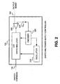
- FIG. 2 is a block diagram illustrating an example switching power supply in accordance with the teachings of the present invention.
- FIG. 3 is a block diagram illustrating an example power bus monitor in accordance with the teachings of the present invention.
- FIG. 4 is a diagram illustrating an example of how a switching frequency can be modulated with encoded information in accordance with the teachings of the present invention.
- FIG. 5 is a diagram illustrating an example of how an output can be encoded with information to identify a power supply for authentication in accordance with the teachings of the present invention.
- a power supply is authenticated using one-way communication from a power supply to an electronic product with no more than two conductors between the power supply and the electronic product in accordance with the teachings of the present invention.
- Information is encoded on a power supply output and not on a separate data line.
- the product decodes the information to identify and/or authenticate the power supply and to respond accordingly.
- the product may refuse to operate with a power supply that it cannot authenticate.
- the product may also change its mode of operation in response to information that it receives from the power supply. For example, the product may perform different power management operations depending on the capability of the power supply or in response to a fault condition within the power supply.
- FIG. 1 shows generally an example of an electronic system 100 including an example of an external switching power supply 105 that provides power to an electronic product 110 in accordance with the teachings of the present invention.
- External switching power supply 105 has an input 120 of voltage V IN and an output 145 of voltage V O 148 and current Io 149.
- External switching power supply 105 includes a switch S1 125 and a controller 135.
- Controller 135 provides a command signal 130 that switches switch S1 125 in response to an output sense signal 140 to regulate output 145.
- Output 145 couples to electronic product 110 through a connector 115.
- Electronic product 110 contains a power bus monitor 150 that couples to the output 145 of power supply 105 that provides power to electronic product 110 through connector 115.
- Power bus monitor 150 responds to variations in voltage or variations in current of the output 145 of external switching power supply 105 to produce an authentication signal 155 that indicates whether or not external switching power supply 105 is authorized to provide power to electronic product 110 in accordance with the teachings of the present invention.
- FIG. 2 shows an example of the switching power supply controller 135 of FIG. 1 in greater detail.
- example switching power supply controller 135 contains an oscillator 215, switching logic 210, an encoder 220, and an error amplifier 205 coupled together.
- Error amplifier 205 receives an output sense signal 140 and a reference signal V REF 225.
- Switching logic 210 responds to oscillator 215, encoder 220, and error amplifier 205 to produce a switch command signal 130 that switches the switch S 125 to produce a desired output 145.
- Encoder 220 may modify the operation of oscillator 215, the value of reference signal 225, and the response of switching logic 220 in a prescribed way to provide information that identifies the power supply to the electronic product in accordance with the teachings of the present invention.
- the term "encoding” or “coding” may be interpreted as just the adding of information content to events. Therefore, it is appreciated that the use of the term “encoding” or “coding” as used herein does not necessarily imply the use of encryption to maintain the security or privacy of the information. The information may or may not be encoded with encryption when "encoded” or “coded” in accordance with the teachings of the present invention.
- FIG. 3 is a block diagram that shows an example of the power bus monitor 150 of FIG. 1 in greater detail.
- power bus monitor 150 includes a signal detector 305, a decoder 310, and a logical comparator 315.
- Signal detector 305 detects patterns of variations in output 145 that are interpreted by decoder 310 and evaluated by logical comparator 315.
- the nodal connection to the power bus in the example illustrated in FIG. 3 would be used to detect variations in the output voltage 148. It is appreciated that in an alternative example, signal detector 305 could be coupled to detect variations in output current 149.
- logical comparator 315 provides a logic output 155 that indicates whether or not an authorized power supply is providing power to the product in accordance with the teachings of the present invention.
- the output of a switching power supply contains a low amplitude ripple component at the switching frequency of switch S1 125.
- the switching power supply controller 135 changes the switching frequency in a prescribed pattern to encode information on the output of the power supply while keeping the output within its specified range in accordance with the teachings of the present invention.
- the switching frequency may be modulated to reduce the average switching noise, as in jittering the switching frequency to reduce electromagnetic interference. Modulation of the switching frequency typically does not change the regulated value of the output, and the modulation is detectible only as a variation in the small amplitude ripple and noise that is present in the output.
- the switching frequency is usually modulated at a constant periodic rate between two values. However, in one example, the frequency is modulated in a pattern that represents binary information to identify the power supply for authentication in accordance with the teachings of the present invention.
- FIG. 4 shows one example of how the switching frequency of the switch S1 125 of FIG. 1 can be modulated with encoded information in accordance with the teachings of the present invention.
- the switching frequency is shifted between a first frequency f SL and a second frequency f SH in a pattern that represents a sequence of bits.
- the shift in switching frequency can be gradual or abrupt.
- the shift of the frequency needs to be only large enough to be detected reliably according to an example of the present invention.
- the encoding illustrated in the example of FIG. 4 will be recognized by one skilled in the art as a Manchester encoding. It is appreciated that the Manchester encoding illustrated in FIG. 4 is only one example of a type of encoding and that other types of encoding data may be employed in accordance with the teachings of the present invention. However, the self-clocking property, ease of generation, and zero average value of Manchester encoded signals make Manchester encoded signals one example of encoding that is well suited for encoding binary information on the output of a switching power supply in accordance with the teachings of the present invention. Thus, referring back to FIG. 1, the cable that connects the external power supply 105 to the electronic product 110 needs no more than two conductors in connector 115. In other words, a third conductor for transferring data or synchronization between external power supply 105 and electronic product 110 is not required in accordance with the teachings of the present invention.
- encoder 220 may include a simple linear feedback shift register that uses a polynomial to generate a sequence of bits that encrypts a binary key in accordance with the teachings of the present invention.
- the manufacturer of the electronic product may specify the polynomial and the key. Modulation of the switching frequency with the desired information can occur intermittently or continuously in accordance with the teachings of the present invention.
- signal detector 305 may use any of several well-known frequency demodulation techniques to extract the binary information from the power bus.
- decoder 310 includes a linear feedback shift register that uses the same encrypting polynomial and key to decrypt the sequence of bits.
- logical comparator 315 recognizes the key, logical output 155 is asserted to authenticate the power supply in accordance with the teachings of the present invention.
- the switching frequency it is not necessary to modulate the switching frequency to encode information that identifies a power supply for authentication.
- the phase of the ripple at the output can be modulated by delaying the switching of the switch by half a switching cycle.
- the information can also be encoded in an output quantity of power supply 105, such as for example the amplitude of an output voltage Vo 148 at output 145 or the amplitude of an output current I O 149 in accordance with the teachings of the present invention.
- FIG. 5 shows one example of how the amplitude of the output voltage Vo 148 of FIG. 1 can be encoded with information to identify a power supply 105 to electronic product 110 for authentication in accordance with the teachings of the present invention.
- authentication may occur for example during start-up.
- the output Vo 145 goes through a sequence of changes in amplitude.
- a start-up event is the application of alternating current (AC) power to the power supply.
- a start-up event is the connection of an output of the power supply to the product.
- the duration that an output voltage Vo 148 is above an upper threshold V UTH is compared to the duration the output voltage Vo 148 is below a lower threshold V LTH during an identification event.
- the lower threshold V LTH is substantially equal to zero volts.
- the controller 135 operates using an on/off control scheme where the average frequency at which switch S1 125 switches varies according to the amount of power delivered to the product 110.
- the authentication event is an event which takes place when the average frequency at which switch S 1 125 switches is within a specific range. While the average switching frequency of S1 of switch S1 125 is within this range, any of the encoding techniques described above can be used such as modulating a magnitude of an output or further modulation of the switching frequency to encode information that can be detected by signal detector 305.
- the encoder 220 of switching power supply controller 135 modulates the reference voltage 225 to modulate the magnitude of the power supply output voltage 140 in accordance with the teachings of the present invention.
- the encoder 220 of switching power supply controller 135 modulates the oscillator 215 or switching logic 210 to completely disable the switching of switch S1 125 to modulate the magnitude of the power supply output voltage 145 in accordance with the teachings of the present invention.
- the controller 135 receives an output sense signal 140 representative of the output voltage 148.
- the authentication event is an event which takes place when the output voltage Vo 148 at output 145 is below a threshold value. While the output voltage is below this threshold value, any of the encoding techniques described above can be used such as modulating a magnitude of an output or modulation of the switching frequency to encode information that can be detected by signal detector 305.
- decoder 310 decodes the sequence and duration of threshold crossings for comparison to a key.
- a key is simply the count of a particular number of transitions within a timing window.
- logical comparator 315 recognizes the key, logical output 155 is asserted to authenticate the power supply in accordance with the teachings of the present invention.
- any of the above described techniques of encoding and decoding can also be applied to allow the power supply 105 to provide information to the electronic product 110 regarding the operating conditions of the external power supply, for example the power consumption of the external power supply or any fault condition that may exist in the operation of the external power supply.
- Providing information about the power supply to the electronic product is also desirable when the power supply is internal to the product as for example, in desktop computers, set top boxes, and TVs.
Landscapes
- Engineering & Computer Science (AREA)
- Power Engineering (AREA)
- Dc-Dc Converters (AREA)
- Power Sources (AREA)
- Charge And Discharge Circuits For Batteries Or The Like (AREA)
Abstract
Description
- Embodiments of the invention relate generally to electronic products and, more specifically but not exclusively relate to electronic products that receive power from external switching power supplies.
- An external power supply is one that remains outside the enclosure of the product, such as the ac adapter for a digital camera, or the dc adapter that allows the product to operate from a power outlet of an automobile. These electronic products usually are small portable units, but products not designed for portability also use external power supplies. For example, some models of small desktop computers use rather large external power supplies.
- Manufacturers of electronic products often prefer to use external power supplies rather than an internal power supply to power their equipment. The use of an external power supply reduces the physical size and weight of the product. Also, the design of the product is not burdened with the need to provide cooling for a power supply if the power supply can simply be procured to the manufacturer's specification as an external component. Typically, the external power supply will connect to the product with a long cable to allow the product to be located at a convenient distance away from the power supply.
- Manufacturers desire to prevent the use of unauthorized or counterfeit external power supplies with their products. The use of a power supply that does not meet the manufacturer's requirements can expose the product or the user to harm. Manufacturers may also desire to receive information regarding the operating conditions of the external power supply as for example the power consumption of the external power supply or any fault condition that may exist within the external power supply. The ability to receive information regarding the operating conditions of the power supply is also desirable in the case of internal power supplies incorporated inside products such as desktop computers and set top boxes. Internal power supplies are enclosed within the product itself as in the case of products such as set top boxes or TVs. In some cases, a power supply may be fully contained within its own separate enclosure, but yet enclosed inside the enclosure of the product such as a desktop computer.
- Non-limiting and non-exhaustive embodiments of the present invention are described with reference to the following figures, wherein like reference numerals refer to like parts throughout the various views unless otherwise specified.
- FIG. 1 is a block diagram illustrating an example electronic system with an external power supply in accordance with the teachings of the present invention.
- FIG. 2 is a block diagram illustrating an example switching power supply in accordance with the teachings of the present invention.
- FIG. 3 is a block diagram illustrating an example power bus monitor in accordance with the teachings of the present invention.
- FIG. 4 is a diagram illustrating an example of how a switching frequency can be modulated with encoded information in accordance with the teachings of the present invention.
- FIG. 5 is a diagram illustrating an example of how an output can be encoded with information to identify a power supply for authentication in accordance with the teachings of the present invention.
- Methods and apparatuses for authenticating a power supply are disclosed. In the following description numerous specific details are set forth in order to provide a thorough understanding of the present invention. It will be apparent, however, to one having ordinary skill in the art that the specific detail need not be employed to practice the present invention. In other instances, well-known materials or methods have not been described in detail in order to avoid obscuring the present invention.
- Reference throughout this specification to "one embodiment" or "an embodiment" means that a particular feature, structure or characteristic described in connection with the embodiment is included in at least one embodiment of the present invention. Thus, appearances of the phrases "in one embodiment" or "in an embodiment" in various places throughout this specification are not necessarily all referring to the same embodiment. Furthermore, the particular features, structures or characteristics may be combined in any suitable manner in one or more embodiments. In addition, it is appreciated that the figures provided herewith are for explanation purposes to persons ordinarily skilled in the art and that the drawings are not necessarily drawn to scale.
- As will be discussed, novel examples for authenticating a power supply are disclosed herein. In one example, a power supply is authenticated using one-way communication from a power supply to an electronic product with no more than two conductors between the power supply and the electronic product in accordance with the teachings of the present invention. Information is encoded on a power supply output and not on a separate data line. The product decodes the information to identify and/or authenticate the power supply and to respond accordingly. The product may refuse to operate with a power supply that it cannot authenticate. The product may also change its mode of operation in response to information that it receives from the power supply. For example, the product may perform different power management operations depending on the capability of the power supply or in response to a fault condition within the power supply.
- To illustrate, FIG. 1 shows generally an example of an
electronic system 100 including an example of an externalswitching power supply 105 that provides power to anelectronic product 110 in accordance with the teachings of the present invention. Externalswitching power supply 105 has aninput 120 of voltage VIN and anoutput 145 ofvoltage V O 148 and current Io 149. Externalswitching power supply 105 includes aswitch S1 125 and acontroller 135.Controller 135 provides acommand signal 130 thatswitches switch S1 125 in response to anoutput sense signal 140 to regulateoutput 145. -
Output 145 couples toelectronic product 110 through aconnector 115.Electronic product 110 contains apower bus monitor 150 that couples to theoutput 145 ofpower supply 105 that provides power toelectronic product 110 throughconnector 115.Power bus monitor 150 responds to variations in voltage or variations in current of theoutput 145 of externalswitching power supply 105 to produce anauthentication signal 155 that indicates whether or not externalswitching power supply 105 is authorized to provide power toelectronic product 110 in accordance with the teachings of the present invention. - FIG. 2 shows an example of the switching
power supply controller 135 of FIG. 1 in greater detail. As shown, example switchingpower supply controller 135 contains anoscillator 215,switching logic 210, anencoder 220, and anerror amplifier 205 coupled together.Error amplifier 205 receives anoutput sense signal 140 and areference signal V REF225. Switchinglogic 210 responds tooscillator 215,encoder 220, anderror amplifier 205 to produce aswitch command signal 130 that switches theswitch S 125 to produce adesired output 145.Encoder 220 may modify the operation ofoscillator 215, the value ofreference signal 225, and the response ofswitching logic 220 in a prescribed way to provide information that identifies the power supply to the electronic product in accordance with the teachings of the present invention. - It is appreciated that in the present disclosure, the term "encoding" or "coding" may be interpreted as just the adding of information content to events. Therefore, it is appreciated that the use of the term "encoding" or "coding" as used herein does not necessarily imply the use of encryption to maintain the security or privacy of the information. The information may or may not be encoded with encryption when "encoded" or "coded" in accordance with the teachings of the present invention.
- FIG. 3 is a block diagram that shows an example of the
power bus monitor 150 of FIG. 1 in greater detail. As shown,power bus monitor 150 includes asignal detector 305, adecoder 310, and alogical comparator 315.Signal detector 305 detects patterns of variations inoutput 145 that are interpreted bydecoder 310 and evaluated bylogical comparator 315. The nodal connection to the power bus in the example illustrated in FIG. 3 would be used to detect variations in theoutput voltage 148. It is appreciated that in an alternative example,signal detector 305 could be coupled to detect variations inoutput current 149. The detected variations in voltage or current could be large such as the presence or absence of a voltage or current, or they could be low amplitude ripples on a much larger dc value of voltage or current. In the illustrated example,logical comparator 315 provides alogic output 155 that indicates whether or not an authorized power supply is providing power to the product in accordance with the teachings of the present invention. - Information may be coded on the output of the switching power supply in several ways. The output of a switching power supply contains a low amplitude ripple component at the switching frequency of
switch S1 125. In one example, the switchingpower supply controller 135 changes the switching frequency in a prescribed pattern to encode information on the output of the power supply while keeping the output within its specified range in accordance with the teachings of the present invention. - In one example, the switching frequency may be modulated to reduce the average switching noise, as in jittering the switching frequency to reduce electromagnetic interference. Modulation of the switching frequency typically does not change the regulated value of the output, and the modulation is detectible only as a variation in the small amplitude ripple and noise that is present in the output. The switching frequency is usually modulated at a constant periodic rate between two values. However, in one example, the frequency is modulated in a pattern that represents binary information to identify the power supply for authentication in accordance with the teachings of the present invention.
- To illustrate, FIG. 4 shows one example of how the switching frequency of the
switch S1 125 of FIG. 1 can be modulated with encoded information in accordance with the teachings of the present invention. In the illustrated example, the switching frequency is shifted between a first frequency fSL and a second frequency fSH in a pattern that represents a sequence of bits. The shift in switching frequency can be gradual or abrupt. The shift of the frequency needs to be only large enough to be detected reliably according to an example of the present invention. - The encoding illustrated in the example of FIG. 4 will be recognized by one skilled in the art as a Manchester encoding. It is appreciated that the Manchester encoding illustrated in FIG. 4 is only one example of a type of encoding and that other types of encoding data may be employed in accordance with the teachings of the present invention. However, the self-clocking property, ease of generation, and zero average value of Manchester encoded signals make Manchester encoded signals one example of encoding that is well suited for encoding binary information on the output of a switching power supply in accordance with the teachings of the present invention. Thus, referring back to FIG. 1, the cable that connects the
external power supply 105 to theelectronic product 110 needs no more than two conductors inconnector 115. In other words, a third conductor for transferring data or synchronization betweenexternal power supply 105 andelectronic product 110 is not required in accordance with the teachings of the present invention. - Referring now to FIG. 2 for an example,
encoder 220 may include a simple linear feedback shift register that uses a polynomial to generate a sequence of bits that encrypts a binary key in accordance with the teachings of the present invention. In use, the manufacturer of the electronic product may specify the polynomial and the key. Modulation of the switching frequency with the desired information can occur intermittently or continuously in accordance with the teachings of the present invention. - Referring now back to FIG. 3, when the switching power supply modulates the switching frequency to encode data on the output of the power supply,
signal detector 305 may use any of several well-known frequency demodulation techniques to extract the binary information from the power bus. In one example,decoder 310 includes a linear feedback shift register that uses the same encrypting polynomial and key to decrypt the sequence of bits. When thelogical comparator 315 recognizes the key,logical output 155 is asserted to authenticate the power supply in accordance with the teachings of the present invention. - In another example, it is not necessary to modulate the switching frequency to encode information that identifies a power supply for authentication. For instance, the phase of the ripple at the output can be modulated by delaying the switching of the switch by half a switching cycle. In yet another example where the switching frequency does not change, the information can also be encoded in an output quantity of
power supply 105, such as for example the amplitude of anoutput voltage Vo 148 atoutput 145 or the amplitude of an output current IO 149 in accordance with the teachings of the present invention. - To illustrate, FIG. 5 shows one example of how the amplitude of the
output voltage Vo 148 of FIG. 1 can be encoded with information to identify apower supply 105 toelectronic product 110 for authentication in accordance with the teachings of the present invention. In one example, authentication may occur for example during start-up. In this example of an authentication event during start-up, theoutput Vo 145 goes through a sequence of changes in amplitude. In one example, a start-up event is the application of alternating current (AC) power to the power supply. In another example, a start-up event is the connection of an output of the power supply to the product. When the authentication is a start-up event, large changes in amplitude typically do not upset the operation of theproduct 110. Information is encoded at the times that the amplitude crosses thresholds in accordance with the teachings of the present invention. In one example, the duration that anoutput voltage Vo 148 is above an upper threshold VUTH is compared to the duration theoutput voltage Vo 148 is below a lower threshold VLTH during an identification event. In one embodiment the lower threshold VLTH is substantially equal to zero volts. - In another example of the present invention, during normal operation, the
controller 135 operates using an on/off control scheme where the average frequency at whichswitch S1 125 switches varies according to the amount of power delivered to theproduct 110. In this example, the authentication event is an event which takes place when the average frequency at which switchS 1 125 switches is within a specific range. While the average switching frequency of S1 ofswitch S1 125 is within this range, any of the encoding techniques described above can be used such as modulating a magnitude of an output or further modulation of the switching frequency to encode information that can be detected bysignal detector 305. - As an example, if the average switching frequency of
switch S 1 125 is below a threshold value, theencoder 220 of switchingpower supply controller 135 modulates thereference voltage 225 to modulate the magnitude of the powersupply output voltage 140 in accordance with the teachings of the present invention. - As a further example, if the average switching frequency of
switch S 1 125 is below a threshold value, theencoder 220 of switchingpower supply controller 135 modulates theoscillator 215 or switchinglogic 210 to completely disable the switching ofswitch S1 125 to modulate the magnitude of the powersupply output voltage 145 in accordance with the teachings of the present invention. - In a further embodiment of the present invention, during normal operation, the
controller 135 receives anoutput sense signal 140 representative of theoutput voltage 148. In this embodiment, the authentication event is an event which takes place when theoutput voltage Vo 148 atoutput 145 is below a threshold value. While the output voltage is below this threshold value, any of the encoding techniques described above can be used such as modulating a magnitude of an output or modulation of the switching frequency to encode information that can be detected bysignal detector 305. - In one example, after
signal detector 305 detects an identification event,decoder 310 decodes the sequence and duration of threshold crossings for comparison to a key. In one example, a key is simply the count of a particular number of transitions within a timing window. Whenlogical comparator 315 recognizes the key,logical output 155 is asserted to authenticate the power supply in accordance with the teachings of the present invention. - In addition to simply authenticating an external power supply, any of the above described techniques of encoding and decoding can also be applied to allow the
power supply 105 to provide information to theelectronic product 110 regarding the operating conditions of the external power supply, for example the power consumption of the external power supply or any fault condition that may exist in the operation of the external power supply. Providing information about the power supply to the electronic product is also desirable when the power supply is internal to the product as for example, in desktop computers, set top boxes, and TVs. - The above description of illustrated embodiments of the invention, including what is described in the Abstract, is not intended to be exhaustive or to be limitation to the precise forms disclosed. While specific embodiments of, and examples for, the invention are described herein for illustrative purposes, various equivalent modifications are possible, as those skilled in the relevant art will recognize. Indeed, it is appreciated that the specific voltages, currents, frequencies, power range values, times, etc., are provided for explanation purposes and that other values may also be employed in other embodiments in accordance with the teachings of the present invention.
- These modifications can be made to embodiments of the invention in light of the above detailed description. The terms used in the following claims should not be construed to limit the invention to the specific embodiments disclosed in the specification and the claims. Rather, the scope is to be determined entirely by the following claims, which are to be construed in accordance with established doctrines of claim interpretation.
Claims (19)
- An external power supply (105) of an electronic product (110) that modulates an output of the power supply with information encoded to identify the power supply to the product.
- A system (100), comprising:an external power supply (105) having an external power supply output (145); andan electronic product (110) coupled to the power supply output to receive power from the external power supply, wherein the electronic product is coupled to identify the power supply by interpreting information encoded on the power supply output.
- A switching power supply (105) having a switching frequency and a switching power supply output (145), the switching frequency coupled to change in a pattern that identifies the switching power supply to an electronic product to be coupled to receive power from the switch power supply output.
- A switching power supply (105) having a switching power supply output (145), the switching power supply coupled to change a magnitude of the switching power supply output in a pattern that identifies the switching power supply to an electronic product to be coupled to receive power from the switching power supply output.
- A switching power supply according to claim 4, wherein the change of the magnitude of the switching power supply output is coupled to occur within a startup interval.
- A switching power supply according to claim 4 or 5, wherein the change of the magnitude of the switching power supply output is coupled to occur when an average switching frequency of the switching power supply is within a range of values.
- A switching power supply according to claim 6, wherein the magnitude of an output voltage (148) of the switching power supply output is coupled to be modulated when the average switching frequency of the switching power supply is within the range of values.
- A switching power supply according to claim 7, wherein the magnitude of the output voltage of the switching power supply output is coupled to be modulated between an upper threshold and a lower threshold value when the average switching frequency of the switching power supply is within the range of values.
- A switching power supply according to claim 8, wherein the magnitude of the output voltage of the switching power supply output is coupled to be modulated between the upper threshold and substantially zero volts when the average switching frequency of the switching power supply is within the range of values.
- A switching power supply according to claim 4 or 5, wherein the change of the magnitude of the switching power supply output is coupled to occur when an output voltage (148) of the switching power supply output is below a threshold value.
- A switching power supply according to claim 10, wherein the magnitude of an output of the switching power supply output is coupled to be modulated further when the output voltage of the switching power supply output is below the threshold value.
- A switching power supply according to claim 11, wherein the magnitude of an output voltage of the switching power supply output is coupled to be modulated between an upper threshold and a lower threshold value when the output voltage of the switching power supply output is below a threshold value.
- A switching power supply according to claim 12, wherein the magnitude of an output voltage of the switching power supply output is coupled to be modulated between an upper threshold and substantially zero volts when the output voltage of the switching power supply output is below the threshold value.
- A switching power supply according to claim 4 or 5, wherein the change of the magnitude of the output of the switching power supply is coupled to occur when an output current of the switching power supply is within a range of values.
- A switching power supply according to claim 4 or 5, wherein the change of the magnitude of the output of the switching power supply is coupled to occur when an output voltage of the switching power supply is within a range of values.
- A power supply (105) of an electronic product (110) that modulates an output (145) of the power supply with information encoded to provide information regarding the operation of the power supply.
- A power supply according to claim 16, wherein the information encoded on the output of the power supply includes information regarding the power consumption of the external power supply.
- A power supply according to claim 16 or 17, wherein the information encoded on the output of the power supply includes information regarding a fault condition that exists within the external power supply.
- A switching power supply according to claim 4 or 5, wherein the switching power supply is coupled to be identified in response to a number of transitions of the switching power supply output within a timing window.
Applications Claiming Priority (1)
| Application Number | Priority Date | Filing Date | Title |
|---|---|---|---|
| US11/311,957 US8225111B2 (en) | 2005-12-19 | 2005-12-19 | Method and apparatus to authenticate a power supply |
Publications (3)
| Publication Number | Publication Date |
|---|---|
| EP1798834A2 true EP1798834A2 (en) | 2007-06-20 |
| EP1798834A3 EP1798834A3 (en) | 2009-05-06 |
| EP1798834B1 EP1798834B1 (en) | 2011-11-09 |
Family
ID=37966442
Family Applications (1)
| Application Number | Title | Priority Date | Filing Date |
|---|---|---|---|
| EP06254827A Not-in-force EP1798834B1 (en) | 2005-12-19 | 2006-09-18 | Method and apparatus to authenticate a power supply |
Country Status (5)
| Country | Link |
|---|---|
| US (2) | US8225111B2 (en) |
| EP (1) | EP1798834B1 (en) |
| JP (1) | JP2007172578A (en) |
| CN (1) | CN101017976B (en) |
| AT (1) | ATE533219T1 (en) |
Cited By (3)
| Publication number | Priority date | Publication date | Assignee | Title |
|---|---|---|---|---|
| WO2014117801A1 (en) * | 2013-01-29 | 2014-08-07 | Phonak Ag | State of charge indication in a hearing device |
| WO2015052052A1 (en) * | 2013-10-07 | 2015-04-16 | Sma Solar Technology Ag | Multistring photovoltaic inverter with identification of interposed dc-dc choppers for deactivating the internal mppt |
| GB2561225A (en) * | 2017-04-06 | 2018-10-10 | Ge Aviation Systems Group Ltd | Power distribution node |
Families Citing this family (22)
| Publication number | Priority date | Publication date | Assignee | Title |
|---|---|---|---|---|
| US9153960B2 (en) | 2004-01-15 | 2015-10-06 | Comarco Wireless Technologies, Inc. | Power supply equipment utilizing interchangeable tips to provide power and a data signal to electronic devices |
| US7868486B2 (en) | 2004-01-15 | 2011-01-11 | Comarco Wireless Technologies, Inc | Power supply having source determination circuitry utilized to disable battery charging circuitry in powered device |
| US7502236B2 (en) | 2006-10-04 | 2009-03-10 | Power Integrations, Inc. | Power supply controller responsive to a feedforward signal |
| US7576528B2 (en) | 2006-10-04 | 2009-08-18 | Power Integrations, Inc. | Control circuit responsive to an impedance |
| US7518885B2 (en) * | 2006-10-04 | 2009-04-14 | Power Integrations, Inc. | Method and apparatus for a control circuit with multiple operation modes |
| US7873845B2 (en) * | 2007-07-11 | 2011-01-18 | Cisco Technology, Inc. | Classification technique for powered devices using selective frequency filtering |
| US9148286B2 (en) * | 2007-10-15 | 2015-09-29 | Finisar Corporation | Protecting against counterfeit electronic devices |
| US8108700B2 (en) * | 2009-03-10 | 2012-01-31 | International Business Machines Corporation | Power supply identification using a modified power good signal |
| US20110099394A1 (en) * | 2009-10-22 | 2011-04-28 | International Business Machines Corporation | Power management in a data processing apparatus |
| US9071066B2 (en) * | 2009-12-22 | 2015-06-30 | Empire Technology Development Llc | Measurement of environmental impact of electronic devices |
| KR20120029656A (en) * | 2010-09-17 | 2012-03-27 | 삼성전자주식회사 | Computer system, power supply apparatus and control method thereof |
| US9385589B2 (en) * | 2011-11-15 | 2016-07-05 | Apple Inc. | Management of common mode noise frequencies in portable electronic devices |
| US9008993B2 (en) * | 2011-12-19 | 2015-04-14 | Blackberry Limited | Methods and apparatus for detecting unauthorized batteries or tampering by monitoring a thermal profile |
| US8471415B1 (en) * | 2012-09-10 | 2013-06-25 | Google Inc. | Identifying a device with a universal power supply by reading a communication tag |
| US9329654B2 (en) * | 2012-10-19 | 2016-05-03 | Dell Products, Lp | System and method for one-line power mapping of information handling systems in a datacenter |
| CN103257945B (en) * | 2013-04-28 | 2016-05-25 | 深圳市芯海科技有限公司 | The method and the device that utilize power line to communicate |
| EP3031121A4 (en) | 2013-08-06 | 2017-02-15 | Bedrock Automation Platforms Inc. | Smart power system |
| US10928794B2 (en) | 2018-01-05 | 2021-02-23 | Emera Technologies LLC | Fault detection systems and methods for power grid systems |
| US12021439B2 (en) | 2019-05-24 | 2024-06-25 | Power Integrations, Inc. | Switching delay for communication |
| FR3102406B1 (en) * | 2019-10-24 | 2021-11-12 | Faiveley Transp Tours | Method for confirming the execution of a consumption reduction order |
| US11418121B2 (en) | 2019-12-30 | 2022-08-16 | Power Integrations, Inc | Auxiliary converter to provide operating power for a controller |
| US11258369B2 (en) | 2020-02-19 | 2022-02-22 | Power Integrations, Inc. | Inductive charging circuit to provide operative power for a controller |
Citations (2)
| Publication number | Priority date | Publication date | Assignee | Title |
|---|---|---|---|---|
| WO2000059127A1 (en) | 1999-03-27 | 2000-10-05 | Binary Electronics Limited | Signalling method and apparatus |
| WO2001093398A2 (en) | 2000-06-02 | 2001-12-06 | Astec International Limited | Automatic module configuration in a telecommunications power system and battery configuration with a click |
Family Cites Families (26)
| Publication number | Priority date | Publication date | Assignee | Title |
|---|---|---|---|---|
| US4737657A (en) | 1986-07-10 | 1988-04-12 | Jatko William B | Interrogator system for identifying electrical circuits |
| US5210846B1 (en) | 1989-05-15 | 1999-06-29 | Dallas Semiconductor | One-wire bus architecture |
| JPH0321139A (en) * | 1989-06-19 | 1991-01-29 | Toshiba Lighting & Technol Corp | Signal processor |
| JP2776644B2 (en) | 1991-04-04 | 1998-07-16 | 茨城日本電気株式会社 | Power supply abnormality monitoring circuit |
| JPH05204483A (en) * | 1992-01-29 | 1993-08-13 | Toshiba Corp | Portable computer |
| US5592069A (en) | 1992-10-07 | 1997-01-07 | Dallas Semiconductor Corporation | Battery charger |
| JPH07143749A (en) | 1993-11-12 | 1995-06-02 | Canon Inc | AC adapter and equipment using AC adapter |
| US5548200A (en) | 1994-07-06 | 1996-08-20 | Norvik Traction Inc. | Universal charging station and method for charging electric vehicle batteries |
| GB9423314D0 (en) | 1994-11-18 | 1995-01-11 | Explosive Dev Ltd | Electrical distribution system |
| GB9524948D0 (en) | 1995-12-06 | 1996-02-07 | Int Computers Ltd | Combined data and power transmission |
| JPH09308096A (en) * | 1996-05-15 | 1997-11-28 | Canon Inc | Power supply |
| US5960084A (en) * | 1996-12-13 | 1999-09-28 | Compaq Computer Corporation | Secure method for enabling/disabling power to a computer system following two-piece user verification |
| US6026126A (en) * | 1997-04-08 | 2000-02-15 | Motorola, Inc. | Method and apparatus for reducing a ripple signal in an output of a direct current power supply |
| JPH11122809A (en) * | 1997-10-16 | 1999-04-30 | Sony Corp | Power supply adapter, electronic equipment and signal transmission system |
| JP3070852B1 (en) | 1999-08-25 | 2000-07-31 | サンケン電気株式会社 | Resonant DC-DC converter |
| JP3625799B2 (en) | 2001-11-30 | 2005-03-02 | 三洋電機株式会社 | Battery pack with authenticity detection circuit |
| JP3704106B2 (en) | 2002-06-28 | 2005-10-05 | 株式会社東芝 | Electronic device and power supply method |
| JP2005012663A (en) * | 2003-06-20 | 2005-01-13 | Sanyo Electric Co Ltd | Authentication system and ID generator |
| JP2005073053A (en) * | 2003-08-26 | 2005-03-17 | Sanyo Electric Co Ltd | Id confirmation unit, id generation unit and authentication system |
| JP2005094128A (en) | 2003-09-12 | 2005-04-07 | Matsushita Electric Ind Co Ltd | Authentication system |
| CN100375942C (en) * | 2003-09-26 | 2008-03-19 | 纬创资通股份有限公司 | System device with identifiable power adapter and identification method |
| JP2005338604A (en) | 2004-05-28 | 2005-12-08 | Toshiba Corp | Projection device and control method of projection device |
| US7296164B2 (en) * | 2004-10-13 | 2007-11-13 | Dell Products L.P. | Power management scheme for external batteries |
| US7392410B2 (en) * | 2004-10-15 | 2008-06-24 | Dell Products L.P. | Power adapter having power supply identifier information functionality |
| JP4986395B2 (en) | 2004-11-25 | 2012-07-25 | ルネサスエレクトロニクス株式会社 | Battery pack and portable electronic device |
| US20070089163A1 (en) | 2005-10-18 | 2007-04-19 | International Business Machines Corporation | System and method for controlling security of a remote network power device |
-
2005
- 2005-12-19 US US11/311,957 patent/US8225111B2/en not_active Expired - Fee Related
-
2006
- 2006-09-18 EP EP06254827A patent/EP1798834B1/en not_active Not-in-force
- 2006-09-18 AT AT06254827T patent/ATE533219T1/en active
- 2006-09-21 JP JP2006255470A patent/JP2007172578A/en active Pending
- 2006-12-19 CN CN2006101675620A patent/CN101017976B/en not_active Expired - Fee Related
-
2012
- 2012-06-06 US US13/490,371 patent/US8499179B2/en not_active Expired - Fee Related
Patent Citations (2)
| Publication number | Priority date | Publication date | Assignee | Title |
|---|---|---|---|---|
| WO2000059127A1 (en) | 1999-03-27 | 2000-10-05 | Binary Electronics Limited | Signalling method and apparatus |
| WO2001093398A2 (en) | 2000-06-02 | 2001-12-06 | Astec International Limited | Automatic module configuration in a telecommunications power system and battery configuration with a click |
Cited By (5)
| Publication number | Priority date | Publication date | Assignee | Title |
|---|---|---|---|---|
| WO2014117801A1 (en) * | 2013-01-29 | 2014-08-07 | Phonak Ag | State of charge indication in a hearing device |
| WO2015052052A1 (en) * | 2013-10-07 | 2015-04-16 | Sma Solar Technology Ag | Multistring photovoltaic inverter with identification of interposed dc-dc choppers for deactivating the internal mppt |
| GB2561225A (en) * | 2017-04-06 | 2018-10-10 | Ge Aviation Systems Group Ltd | Power distribution node |
| GB2561225B (en) * | 2017-04-06 | 2020-02-19 | Ge Aviation Systems Group Ltd | Power distribution node |
| US10644512B2 (en) | 2017-04-06 | 2020-05-05 | Ge Aviation Systems Limited | Power distribution node |
Also Published As
| Publication number | Publication date |
|---|---|
| US20070143636A1 (en) | 2007-06-21 |
| CN101017976A (en) | 2007-08-15 |
| EP1798834A3 (en) | 2009-05-06 |
| US8225111B2 (en) | 2012-07-17 |
| CN101017976B (en) | 2012-10-03 |
| ATE533219T1 (en) | 2011-11-15 |
| US20120246495A1 (en) | 2012-09-27 |
| US8499179B2 (en) | 2013-07-30 |
| EP1798834B1 (en) | 2011-11-09 |
| JP2007172578A (en) | 2007-07-05 |
Similar Documents
| Publication | Publication Date | Title |
|---|---|---|
| US8499179B2 (en) | Method and apparatus to authenticate a power supply | |
| US11394242B2 (en) | Wireless power transfer in-band communication circuit and method | |
| US9026046B2 (en) | Load modulating regulator for a near filed communication device | |
| KR101400695B1 (en) | A clock signal generator capable of generating a stable clock signal, a semiconductor memory device having the clock signal generator, and a method | |
| CN101127071B (en) | Information processing system, and information processing apparatus and method | |
| JP5725895B2 (en) | Power supply system | |
| US10367489B2 (en) | Systems and methods for transferring power across an isolation barrier | |
| US20240370532A1 (en) | Security through layers in an intelligent electronic device | |
| US20120293136A1 (en) | Dual-interface card reader module | |
| WO1999053627A1 (en) | System for communicating with electronic equipment on a network | |
| US20070108301A1 (en) | Semiconductor device and IC card | |
| KR101727964B1 (en) | Device capable of compensating current thereof and memory device | |
| US20200081509A1 (en) | Verification device and verification target device that operates using operation power supplied from the verification device | |
| CN104243888B (en) | A kind of data processing method and display terminal | |
| JP2621414B2 (en) | Information processing device having cordless keyboard | |
| JP4681837B2 (en) | Control device, smart card read activation device and related products | |
| TW466391B (en) | Dynamic series voltage compensator and method thereof | |
| US8076970B2 (en) | Adaptive demodulator | |
| CN107070504B (en) | communication device | |
| CN110945744B (en) | Digital Shunt Regulation for Wireless Power Receivers | |
| CN103259245A (en) | Protection circuit and protection method of electronic device | |
| CN110036596B (en) | Phase-shift coding method and encoder and decoder for signal transition minimization | |
| CN216901660U (en) | Multifunctional USB HUB embedded encryption communication module circuit and device | |
| US20180165900A1 (en) | Intelligent authentication system and electronic key thereof | |
| Gupta et al. | A ubiquitous sensor network for domestic energy monitoring and energy consumption optimization |
Legal Events
| Date | Code | Title | Description |
|---|---|---|---|
| PUAI | Public reference made under article 153(3) epc to a published international application that has entered the european phase |
Free format text: ORIGINAL CODE: 0009012 |
|
| AK | Designated contracting states |
Kind code of ref document: A2 Designated state(s): AT BE BG CH CY CZ DE DK EE ES FI FR GB GR HU IE IS IT LI LT LU LV MC NL PL PT RO SE SI SK TR |
|
| AX | Request for extension of the european patent |
Extension state: AL BA HR MK YU |
|
| RAP3 | Party data changed (applicant data changed or rights of an application transferred) |
Owner name: POWER INTEGRATIONS, INC. |
|
| PUAL | Search report despatched |
Free format text: ORIGINAL CODE: 0009013 |
|
| AK | Designated contracting states |
Kind code of ref document: A3 Designated state(s): AT BE BG CH CY CZ DE DK EE ES FI FR GB GR HU IE IS IT LI LT LU LV MC NL PL PT RO SE SI SK TR |
|
| AX | Request for extension of the european patent |
Extension state: AL BA HR MK RS |
|
| 17P | Request for examination filed |
Effective date: 20090706 |
|
| AKX | Designation fees paid |
Designated state(s): AT BE BG CH CY CZ DE DK EE ES FI FR GB GR HU IE IS IT LI LT LU LV MC NL PL PT RO SE SI SK TR |
|
| 17Q | First examination report despatched |
Effective date: 20100701 |
|
| GRAP | Despatch of communication of intention to grant a patent |
Free format text: ORIGINAL CODE: EPIDOSNIGR1 |
|
| GRAS | Grant fee paid |
Free format text: ORIGINAL CODE: EPIDOSNIGR3 |
|
| GRAA | (expected) grant |
Free format text: ORIGINAL CODE: 0009210 |
|
| AK | Designated contracting states |
Kind code of ref document: B1 Designated state(s): AT BE BG CH CY CZ DE DK EE ES FI FR GB GR HU IE IS IT LI LT LU LV MC NL PL PT RO SE SI SK TR |
|
| REG | Reference to a national code |
Ref country code: GB Ref legal event code: FG4D |
|
| REG | Reference to a national code |
Ref country code: CH Ref legal event code: EP |
|
| REG | Reference to a national code |
Ref country code: IE Ref legal event code: FG4D |
|
| REG | Reference to a national code |
Ref country code: DE Ref legal event code: R096 Ref document number: 602006025686 Country of ref document: DE Effective date: 20120119 |
|
| REG | Reference to a national code |
Ref country code: NL Ref legal event code: T3 |
|
| REG | Reference to a national code |
Ref country code: SE Ref legal event code: TRGR |
|
| LTIE | Lt: invalidation of european patent or patent extension |
Effective date: 20111109 |
|
| PG25 | Lapsed in a contracting state [announced via postgrant information from national office to epo] |
Ref country code: IS Free format text: LAPSE BECAUSE OF FAILURE TO SUBMIT A TRANSLATION OF THE DESCRIPTION OR TO PAY THE FEE WITHIN THE PRESCRIBED TIME-LIMIT Effective date: 20120309 Ref country code: LT Free format text: LAPSE BECAUSE OF FAILURE TO SUBMIT A TRANSLATION OF THE DESCRIPTION OR TO PAY THE FEE WITHIN THE PRESCRIBED TIME-LIMIT Effective date: 20111109 |
|
| PG25 | Lapsed in a contracting state [announced via postgrant information from national office to epo] |
Ref country code: SI Free format text: LAPSE BECAUSE OF FAILURE TO SUBMIT A TRANSLATION OF THE DESCRIPTION OR TO PAY THE FEE WITHIN THE PRESCRIBED TIME-LIMIT Effective date: 20111109 Ref country code: GR Free format text: LAPSE BECAUSE OF FAILURE TO SUBMIT A TRANSLATION OF THE DESCRIPTION OR TO PAY THE FEE WITHIN THE PRESCRIBED TIME-LIMIT Effective date: 20120210 Ref country code: LV Free format text: LAPSE BECAUSE OF FAILURE TO SUBMIT A TRANSLATION OF THE DESCRIPTION OR TO PAY THE FEE WITHIN THE PRESCRIBED TIME-LIMIT Effective date: 20111109 Ref country code: BE Free format text: LAPSE BECAUSE OF FAILURE TO SUBMIT A TRANSLATION OF THE DESCRIPTION OR TO PAY THE FEE WITHIN THE PRESCRIBED TIME-LIMIT Effective date: 20111109 Ref country code: PT Free format text: LAPSE BECAUSE OF FAILURE TO SUBMIT A TRANSLATION OF THE DESCRIPTION OR TO PAY THE FEE WITHIN THE PRESCRIBED TIME-LIMIT Effective date: 20120309 Ref country code: PL Free format text: LAPSE BECAUSE OF FAILURE TO SUBMIT A TRANSLATION OF THE DESCRIPTION OR TO PAY THE FEE WITHIN THE PRESCRIBED TIME-LIMIT Effective date: 20111109 |
|
| PG25 | Lapsed in a contracting state [announced via postgrant information from national office to epo] |
Ref country code: CY Free format text: LAPSE BECAUSE OF FAILURE TO SUBMIT A TRANSLATION OF THE DESCRIPTION OR TO PAY THE FEE WITHIN THE PRESCRIBED TIME-LIMIT Effective date: 20111109 |
|
| PG25 | Lapsed in a contracting state [announced via postgrant information from national office to epo] |
Ref country code: BG Free format text: LAPSE BECAUSE OF FAILURE TO SUBMIT A TRANSLATION OF THE DESCRIPTION OR TO PAY THE FEE WITHIN THE PRESCRIBED TIME-LIMIT Effective date: 20120209 Ref country code: SK Free format text: LAPSE BECAUSE OF FAILURE TO SUBMIT A TRANSLATION OF THE DESCRIPTION OR TO PAY THE FEE WITHIN THE PRESCRIBED TIME-LIMIT Effective date: 20111109 Ref country code: EE Free format text: LAPSE BECAUSE OF FAILURE TO SUBMIT A TRANSLATION OF THE DESCRIPTION OR TO PAY THE FEE WITHIN THE PRESCRIBED TIME-LIMIT Effective date: 20111109 Ref country code: CZ Free format text: LAPSE BECAUSE OF FAILURE TO SUBMIT A TRANSLATION OF THE DESCRIPTION OR TO PAY THE FEE WITHIN THE PRESCRIBED TIME-LIMIT Effective date: 20111109 Ref country code: DK Free format text: LAPSE BECAUSE OF FAILURE TO SUBMIT A TRANSLATION OF THE DESCRIPTION OR TO PAY THE FEE WITHIN THE PRESCRIBED TIME-LIMIT Effective date: 20111109 |
|
| PG25 | Lapsed in a contracting state [announced via postgrant information from national office to epo] |
Ref country code: RO Free format text: LAPSE BECAUSE OF FAILURE TO SUBMIT A TRANSLATION OF THE DESCRIPTION OR TO PAY THE FEE WITHIN THE PRESCRIBED TIME-LIMIT Effective date: 20111109 |
|
| PLBE | No opposition filed within time limit |
Free format text: ORIGINAL CODE: 0009261 |
|
| STAA | Information on the status of an ep patent application or granted ep patent |
Free format text: STATUS: NO OPPOSITION FILED WITHIN TIME LIMIT |
|
| REG | Reference to a national code |
Ref country code: AT Ref legal event code: MK05 Ref document number: 533219 Country of ref document: AT Kind code of ref document: T Effective date: 20111109 |
|
| 26N | No opposition filed |
Effective date: 20120810 |
|
| REG | Reference to a national code |
Ref country code: DE Ref legal event code: R097 Ref document number: 602006025686 Country of ref document: DE Effective date: 20120810 |
|
| PG25 | Lapsed in a contracting state [announced via postgrant information from national office to epo] |
Ref country code: AT Free format text: LAPSE BECAUSE OF FAILURE TO SUBMIT A TRANSLATION OF THE DESCRIPTION OR TO PAY THE FEE WITHIN THE PRESCRIBED TIME-LIMIT Effective date: 20111109 |
|
| PG25 | Lapsed in a contracting state [announced via postgrant information from national office to epo] |
Ref country code: ES Free format text: LAPSE BECAUSE OF FAILURE TO SUBMIT A TRANSLATION OF THE DESCRIPTION OR TO PAY THE FEE WITHIN THE PRESCRIBED TIME-LIMIT Effective date: 20120220 Ref country code: MC Free format text: LAPSE BECAUSE OF NON-PAYMENT OF DUE FEES Effective date: 20120930 |
|
| REG | Reference to a national code |
Ref country code: CH Ref legal event code: PL |
|
| REG | Reference to a national code |
Ref country code: IE Ref legal event code: MM4A |
|
| PG25 | Lapsed in a contracting state [announced via postgrant information from national office to epo] |
Ref country code: FI Free format text: LAPSE BECAUSE OF FAILURE TO SUBMIT A TRANSLATION OF THE DESCRIPTION OR TO PAY THE FEE WITHIN THE PRESCRIBED TIME-LIMIT Effective date: 20111109 |
|
| PG25 | Lapsed in a contracting state [announced via postgrant information from national office to epo] |
Ref country code: IE Free format text: LAPSE BECAUSE OF NON-PAYMENT OF DUE FEES Effective date: 20120918 Ref country code: CH Free format text: LAPSE BECAUSE OF NON-PAYMENT OF DUE FEES Effective date: 20120930 Ref country code: LI Free format text: LAPSE BECAUSE OF NON-PAYMENT OF DUE FEES Effective date: 20120930 |
|
| PGFP | Annual fee paid to national office [announced via postgrant information from national office to epo] |
Ref country code: SE Payment date: 20130927 Year of fee payment: 8 |
|
| PG25 | Lapsed in a contracting state [announced via postgrant information from national office to epo] |
Ref country code: TR Free format text: LAPSE BECAUSE OF FAILURE TO SUBMIT A TRANSLATION OF THE DESCRIPTION OR TO PAY THE FEE WITHIN THE PRESCRIBED TIME-LIMIT Effective date: 20111109 |
|
| PG25 | Lapsed in a contracting state [announced via postgrant information from national office to epo] |
Ref country code: LU Free format text: LAPSE BECAUSE OF NON-PAYMENT OF DUE FEES Effective date: 20120918 |
|
| PG25 | Lapsed in a contracting state [announced via postgrant information from national office to epo] |
Ref country code: HU Free format text: LAPSE BECAUSE OF FAILURE TO SUBMIT A TRANSLATION OF THE DESCRIPTION OR TO PAY THE FEE WITHIN THE PRESCRIBED TIME-LIMIT Effective date: 20060918 |
|
| PGFP | Annual fee paid to national office [announced via postgrant information from national office to epo] |
Ref country code: FR Payment date: 20140917 Year of fee payment: 9 Ref country code: GB Payment date: 20140929 Year of fee payment: 9 |
|
| PGFP | Annual fee paid to national office [announced via postgrant information from national office to epo] |
Ref country code: IT Payment date: 20140923 Year of fee payment: 9 |
|
| PGFP | Annual fee paid to national office [announced via postgrant information from national office to epo] |
Ref country code: NL Payment date: 20140926 Year of fee payment: 9 |
|
| REG | Reference to a national code |
Ref country code: SE Ref legal event code: EUG |
|
| PG25 | Lapsed in a contracting state [announced via postgrant information from national office to epo] |
Ref country code: SE Free format text: LAPSE BECAUSE OF NON-PAYMENT OF DUE FEES Effective date: 20140919 |
|
| PG25 | Lapsed in a contracting state [announced via postgrant information from national office to epo] |
Ref country code: IT Free format text: LAPSE BECAUSE OF NON-PAYMENT OF DUE FEES Effective date: 20150918 |
|
| GBPC | Gb: european patent ceased through non-payment of renewal fee |
Effective date: 20150918 |
|
| REG | Reference to a national code |
Ref country code: NL Ref legal event code: MM Effective date: 20151001 |
|
| REG | Reference to a national code |
Ref country code: FR Ref legal event code: ST Effective date: 20160531 |
|
| PG25 | Lapsed in a contracting state [announced via postgrant information from national office to epo] |
Ref country code: GB Free format text: LAPSE BECAUSE OF NON-PAYMENT OF DUE FEES Effective date: 20150918 |
|
| PG25 | Lapsed in a contracting state [announced via postgrant information from national office to epo] |
Ref country code: NL Free format text: LAPSE BECAUSE OF NON-PAYMENT OF DUE FEES Effective date: 20151001 Ref country code: FR Free format text: LAPSE BECAUSE OF NON-PAYMENT OF DUE FEES Effective date: 20150930 |
|
| PGFP | Annual fee paid to national office [announced via postgrant information from national office to epo] |
Ref country code: DE Payment date: 20160928 Year of fee payment: 11 |
|
| REG | Reference to a national code |
Ref country code: DE Ref legal event code: R119 Ref document number: 602006025686 Country of ref document: DE |
|
| PG25 | Lapsed in a contracting state [announced via postgrant information from national office to epo] |
Ref country code: DE Free format text: LAPSE BECAUSE OF NON-PAYMENT OF DUE FEES Effective date: 20180404 |
|
| P01 | Opt-out of the competence of the unified patent court (upc) registered |
Effective date: 20230502 |