EP1798763A1 - Semiconductor device and die bonding method therefor - Google Patents
Semiconductor device and die bonding method therefor Download PDFInfo
- Publication number
- EP1798763A1 EP1798763A1 EP06019205A EP06019205A EP1798763A1 EP 1798763 A1 EP1798763 A1 EP 1798763A1 EP 06019205 A EP06019205 A EP 06019205A EP 06019205 A EP06019205 A EP 06019205A EP 1798763 A1 EP1798763 A1 EP 1798763A1
- Authority
- EP
- European Patent Office
- Prior art keywords
- solder
- metal
- metal film
- semiconductor device
- melting point
- Prior art date
- Legal status (The legal status is an assumption and is not a legal conclusion. Google has not performed a legal analysis and makes no representation as to the accuracy of the status listed.)
- Granted
Links
Images


Classifications
-
- H—ELECTRICITY
- H10—SEMICONDUCTOR DEVICES; ELECTRIC SOLID-STATE DEVICES NOT OTHERWISE PROVIDED FOR
- H10W—GENERIC PACKAGES, INTERCONNECTIONS, CONNECTORS OR OTHER CONSTRUCTIONAL DETAILS OF DEVICES COVERED BY CLASS H10
- H10W70/00—Package substrates; Interposers; Redistribution layers [RDL]
- H10W70/40—Leadframes
- H10W70/411—Chip-supporting parts, e.g. die pads
- H10W70/417—Bonding materials between chips and die pads
-
- H—ELECTRICITY
- H10—SEMICONDUCTOR DEVICES; ELECTRIC SOLID-STATE DEVICES NOT OTHERWISE PROVIDED FOR
- H10W—GENERIC PACKAGES, INTERCONNECTIONS, CONNECTORS OR OTHER CONSTRUCTIONAL DETAILS OF DEVICES COVERED BY CLASS H10
- H10W72/00—Interconnections or connectors in packages
- H10W72/071—Connecting or disconnecting
- H10W72/073—Connecting or disconnecting of die-attach connectors
-
- H—ELECTRICITY
- H10—SEMICONDUCTOR DEVICES; ELECTRIC SOLID-STATE DEVICES NOT OTHERWISE PROVIDED FOR
- H10W—GENERIC PACKAGES, INTERCONNECTIONS, CONNECTORS OR OTHER CONSTRUCTIONAL DETAILS OF DEVICES COVERED BY CLASS H10
- H10W72/00—Interconnections or connectors in packages
- H10W72/071—Connecting or disconnecting
- H10W72/073—Connecting or disconnecting of die-attach connectors
- H10W72/07331—Connecting techniques
- H10W72/07336—Soldering or alloying
-
- H—ELECTRICITY
- H10—SEMICONDUCTOR DEVICES; ELECTRIC SOLID-STATE DEVICES NOT OTHERWISE PROVIDED FOR
- H10W—GENERIC PACKAGES, INTERCONNECTIONS, CONNECTORS OR OTHER CONSTRUCTIONAL DETAILS OF DEVICES COVERED BY CLASS H10
- H10W72/00—Interconnections or connectors in packages
- H10W72/30—Die-attach connectors
-
- H—ELECTRICITY
- H10—SEMICONDUCTOR DEVICES; ELECTRIC SOLID-STATE DEVICES NOT OTHERWISE PROVIDED FOR
- H10W—GENERIC PACKAGES, INTERCONNECTIONS, CONNECTORS OR OTHER CONSTRUCTIONAL DETAILS OF DEVICES COVERED BY CLASS H10
- H10W72/00—Interconnections or connectors in packages
- H10W72/30—Die-attach connectors
- H10W72/321—Structures or relative sizes of die-attach connectors
- H10W72/325—Die-attach connectors having a filler embedded in a matrix
-
- H—ELECTRICITY
- H10—SEMICONDUCTOR DEVICES; ELECTRIC SOLID-STATE DEVICES NOT OTHERWISE PROVIDED FOR
- H10W—GENERIC PACKAGES, INTERCONNECTIONS, CONNECTORS OR OTHER CONSTRUCTIONAL DETAILS OF DEVICES COVERED BY CLASS H10
- H10W72/00—Interconnections or connectors in packages
- H10W72/30—Die-attach connectors
- H10W72/351—Materials of die-attach connectors
-
- H—ELECTRICITY
- H10—SEMICONDUCTOR DEVICES; ELECTRIC SOLID-STATE DEVICES NOT OTHERWISE PROVIDED FOR
- H10W—GENERIC PACKAGES, INTERCONNECTIONS, CONNECTORS OR OTHER CONSTRUCTIONAL DETAILS OF DEVICES COVERED BY CLASS H10
- H10W72/00—Interconnections or connectors in packages
- H10W72/30—Die-attach connectors
- H10W72/351—Materials of die-attach connectors
- H10W72/352—Materials of die-attach connectors comprising metals or metalloids, e.g. solders
-
- H—ELECTRICITY
- H10—SEMICONDUCTOR DEVICES; ELECTRIC SOLID-STATE DEVICES NOT OTHERWISE PROVIDED FOR
- H10W—GENERIC PACKAGES, INTERCONNECTIONS, CONNECTORS OR OTHER CONSTRUCTIONAL DETAILS OF DEVICES COVERED BY CLASS H10
- H10W72/00—Interconnections or connectors in packages
- H10W72/50—Bond wires
- H10W72/59—Bond pads specially adapted therefor
-
- H—ELECTRICITY
- H10—SEMICONDUCTOR DEVICES; ELECTRIC SOLID-STATE DEVICES NOT OTHERWISE PROVIDED FOR
- H10W—GENERIC PACKAGES, INTERCONNECTIONS, CONNECTORS OR OTHER CONSTRUCTIONAL DETAILS OF DEVICES COVERED BY CLASS H10
- H10W90/00—Package configurations
- H10W90/701—Package configurations characterised by the relative positions of pads or connectors relative to package parts
- H10W90/731—Package configurations characterised by the relative positions of pads or connectors relative to package parts of die-attach connectors
- H10W90/736—Package configurations characterised by the relative positions of pads or connectors relative to package parts of die-attach connectors between a chip and a stacked lead frame, conducting package substrate or heat sink
Definitions
- the present invention relates to a semiconductor device and a die bonding method therefore.
- the present invention is preferably used when a semiconductor device is kept at high temperature for a long time during soldering process.
- the chips are usually subjected to elevated temperature for a long time using a heater. Specifically, the semiconductor chips are exposed to high temperature conditions until their die boding is complete. Therefore, during this die bonding process, the solder as the bonding material is in a liquid state and hence rapidly diffuses. If this diffusion proceeds extremely, the solder may reach the base material of the lead frames beyond the barrier metal, for example. This results in formation of voids within the solder layer, leading to a reduction in the bonding strength and an increase in the thermal resistance.
- a high melting point solder such as AuSn eutectic solder
- a conventional method for preventing the solder from diffusing to the base material of the frames is to limit the number of chips that can be die-bonded at one time and thereby reduce the die bonding time.
- a QFN package manufacturing process that molds a plurality of packages together currently includes a die bonding process in which the semiconductor chips are subjected to high temperature conditions for a long time.
- the solder layer for bonding the semiconductor chips is exposed to elevated temperature and hence is in a liquid state until a predetermined number of chips are die-bonded.
- the solder When the solder is in a liquid state, it rapidly forms an inter-metallic compound, since its diffusion rate is very high between metals.
- the back side of the semiconductor chip is composed of Ni/Au
- the lead frame side is composed of Cu/Ni/Au
- a solder composed of AuSn is used as the die bonding material.
- the solder of AuSn forms an inter-metallic compound of Sn-Ni with Ni included in the semiconductor side and in the lead frame side.
- the solder of AuSn is in a liquid state as described above, the formation of the inter-metallic compound rapidly proceeds. Therefore, the solder diffuses to the base material Cu of the lead frame through the Ni plating. As a result, voids corresponding to the volume of the solder that has diffused to the Cu base material are formed within the solder layer, resulting in an increase in the thermal resistance of the semiconductor chip and a large reduction in the bonding strength.
- Figs. 9 and 10 illustrate these problems.
- Fig. 9 shows the structure of a conventional semiconductor chip.
- reference numeral 1 denotes GaAs
- 2 denotes Ni
- 3 denotes Au.
- Fig. 10 shows a vertical cross-sectional view of a package in which the semiconductor chip shown in Fig. 9 is die-bonded to a lead frame through application of excessive heat.
- reference numeral 4 denotes a solder formed of AuSn
- 5 denotes voids
- 6 denotes the lead frame.
- voids are formed within the solder layer, resulting in reduction in the bonding strength and an increase in the thermal resistance.
- a semiconductor device comprises a semiconductor substrate, a first metal film formed on a back surface of the semiconductor substrate, a second metal film formed on the first metal film, and a third metal film formed on the second metal film.
- the first metal film forms an alloy with a solder.
- the second metal film causes isothermal solidification of the solder.
- the third metal film is for improving solder wetting property or for inhibiting oxidation.
- a specific type of metal is diffused into a solder, when a solder melts, to transform the solder into a high melting point metal compound, thereby causing isothermal solidification of the solder.
- the specific type of metal is different from the metal of the solder.
- the present invention provides a semiconductor device and a die-bonding method therefor capable of reducing voids formed in the solder joint portions to prevent an increase in the thermal resistance, as well as to prevent a reduction in the strength of the solder joint portions. Accordingly, the present invention leads to improving the quality of semiconductor devices and reducing their cost. Other and further objects, features and advantages of the invention will appear more fully from the following description.
- Figs. 1 to 5 show a semiconductor device and a die bonding method therefor according to a first embodiment of the present invention.
- the chip is usually subjected to an elevated temperature higher than the melting point of the solder, causing the solder layer to assume a liquid state.
- the diffusion rate of the solder becomes extremely high, leading to "abnormal diffusion" of the solder and formation of voids.
- the diffusion rate of the solder must be reduced to prevent formation of voids. This requires that, when the die bonding has been completed, the melting point of the solder be increased to higher than the die bonding temperature so that the solder returns to a solid state.
- a solder bonding layer metal is formed on the back surface of the semiconductor chip, and a special metal for elevating the melting point of the solder is added to the solder bonding layer metal.
- the special metal diffuses within the solder and, as a result, the solder assumes an "isothermal solidification state". Since the solder becomes to a solid state, its diffusion rate is low even under high temperature conditions, thus preventing formation of voids.
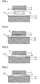
- Fig. 1 is a cross-sectional view showing a chip structure of a semiconductor device according to the first embodiment of the present invention.
- Fig. 1 also shows a cross-section of a lead frame to which the semiconductor chip is soldered.
- a semiconductor chip or a semiconductor device comprises a semiconductor substrate 7, a solder bonding layer metal 8 as a first metal film, a melting point elevating metal 9 as a second metal film, a metal 10 as a third metal film for improving solder wetting property or for inhibiting oxidation.
- the first metal film 8 is formed on the back surface of the semiconductor substrate 7.
- the second metal film 9 is formed on the first metal film 8.
- the third metal film 10 is formed on the second metal film 9.
- Reference numeral 11 shows a solder.
- a lead frame includes oxidation inhibiting metal plating 12, solder-bonding layer metal plating 13 and a lead frame base metal 14.
- the solder 11 is formed of AuSn
- the solder bonding layer metal 8 of Ni the melting point elevating metal 9 of Ti
- the metal 10 of Au for improving solder wetting property are formed in that order on the back side of the semiconductor substrate 7.
- the solder bonding layer metal Ni 8 is a bonding metal (a metal film) for forming an Sn-Ni alloy with the solder 11 of AuSn.
- the underlying melting point elevating metal 9 is a metal film used as an additive to transform the solder 11 into a high melting point metal compound when the solder melts under high temperature conditions. Specifically, when the solder 11 is formed of AuSn, the melting point elevating metal Ti 9 diffuses into the solder 11 and thereby elevates the melting point of the solder 11, so that the solder 11 assumes an "isothermal solidification state".
- the metal Au 10 for improving solder wetting property or inhibiting oxidation is a metal film used to prevent oxidation of the solder bonding layer metal 8 and the melting point elevating metal 9, as well as to improve the wetting between these metals and the solder 11.
- a lead frame made up of the oxidation inhibiting metal plating 12, the solder-bonding layer metal plating 13, and the lead frame base metal 14 is set above a heater at approximately 310°C. Then, the solder 11 is placed at a predetermined die bonding position. After the solder 11 melts, a semiconductor chip having the above metal composition is mounted on it.
- reference numeral 15 shows a state where the metal 10 for improving solder wetting property is dissolved into the solder 11.
- Fig.2 shows that the metal Au 10, shown in Fig. 1, for improving solder wetting property, which is the first to come into contact with the solder 11 of AuSn instantaneously diffuses within the solder 11.
- Fig. 3 shows that the melting point elevating metal Ti 9 has come in contact with the solder 11 of AuSn after the metal 10 has diffused into the solder 11.
- reference numeral 16 shows a state where the melting point elevating metal 9 has begun to diffuse into the state 15, i.e. the state in which the metal 10 for improving solder wetting properties is dissolved into the solder 11.
- reference numeral 17 shows a state where the melting point elevating metal 9 has diffused completely into the state 15, i.e. the state in which the metal 10 for improving solder wetting properties is dissolved into the solder 11.
- solder 11 forms an Sn-Ni alloy layer 18 with the solder bonding layer metal 8, completing the bonding process, as shown in Fig. 5.
- a melting point elevating metal Ti diffuses into the solder 11, causing the melting point of the solder 11 to increase.
- the solder 11 assumes a solid state and remains in this state even at a heater temperature of 310°C.
- the solder 11 in this state does not significantly diffuse even when the semiconductor chip is left at elevated temperature for a long time, preventing formation of excessive inter-metallic compounds. Therefore, no voids are formed within the solder joint portion, thus preventing an increase in the thermal resistance and hence maintaining reliability of the solder joint portion.
- a Ti content of 10 -4 wt% or more should be diffused in the solder 11 of AuSn, since if the Ti content is low, the melting point of the solder 11 does not sufficiently increase and hence isothermal solidification of the solder 11 does not occur.
- Figs. 6 and 7 show a semiconductor device and a die bonding method therefor according to a second embodiment of the present invention.
- the melting point elevating metal 9 is Ti
- the melting point elevating metal 9 may be Pt with the same effect.
- the melting point elevating metal 9 is deposited in stripes on the back surface of the semiconductor chip to allow the metal to uniformly diffuse into the solder.
- Fig. 6 shows the back surface of the semiconductor chip with the oxidation inhibiting metal 22 removed
- Fig. 7 shows a cross-sectional view of the semiconductor chip.
- the semiconductor chip comprises a melting point elevating metal 19, a solder bonding layer metal 20; a semiconductor substrate 21, and a metal 22 for improving solder wetting property or inhibiting oxidation.
- the melting point elevating metal 19 is Pt. Therefore, as in the first embodiment, the solder 11 does not significantly diffuse even when the semiconductor chip is left at elevated temperature for a long time, preventing formation of excessive inter-metallic compounds. As a result, no voids are formed within the solder joint portion, thus preventing an increase in the thermal resistance and hence maintaining reliability of the solder joint portion.
- Fig. 8 shows a cross-sectional view of a semiconductor chip of a semiconductor device according to a third embodiment of the present invention.
- the semiconductor chip comprises a semiconductor substrate 21 and a solder bonding layer metal 23 uniformly containing the melting point elevating metal 19 of the second embodiment.
- Reference numeral 22 shows a metal for improving solder wetting property or inhibiting oxidation.
- the melting point elevating metal 19 is powdered and mixed in the solder bonding layer metal 20 to allow the melting point elevating metal 19 to uniformly diffuse into the solder.
- the present embodiment has the same effect as the second embodiment. Furthermore, since the melting point elevating metal 19 is powdered and uniformly mixed in the solder bonding layer, the reliability of the bonding process is enhanced, resulting in an increase in the quality of the semiconductor device.
- a method for die-bonding a semiconductor device is described.
- a specific type of metal is diffused into a solder when the solder melts, and transform the solder into a high melting point metal compound.
- the specific type of metal is different from the metal of the solder. Thereby, isothermal solidification of the solder is caused.
- the solder contains at least Au or Sn, and the specific type of metal is preferably selected from the group consisting of Ti, Pt, Mo, V, and Nb. Further, the specific type of metal is preferably diffused into the solder at ratio between 1.0 ⁇ 10 -4 wt% and 20 wt%, inclusive.
Landscapes
- Die Bonding (AREA)
Abstract
Description
- The present invention relates to a semiconductor device and a die bonding method therefore. The present invention is preferably used when a semiconductor device is kept at high temperature for a long time during soldering process.
- In the case of a quad flat no-lead (QFN) package manufacturing process that molds a plurality of packages together and that requires the semiconductor chips to be die-bonded by use of a high melting point solder such as AuSn eutectic solder, the chips are usually subjected to elevated temperature for a long time using a heater.
Specifically, the semiconductor chips are exposed to high temperature conditions until their die boding is complete. Therefore, during this die bonding process, the solder as the bonding material is in a liquid state and hence rapidly diffuses. If this diffusion proceeds extremely, the solder may reach the base material of the lead frames beyond the barrier metal, for example. This results in formation of voids within the solder layer, leading to a reduction in the bonding strength and an increase in the thermal resistance. - A conventional method for preventing the solder from diffusing to the base material of the frames is to limit the number of chips that can be die-bonded at one time and thereby reduce the die bonding time. However, this leads to a great reduction in the number of lead frames that can be obtained per unit volume of the material, resulting in increased material cost (see, e.g.,
Japanese Patent Laid-Open No. 06-007990 - A QFN package manufacturing process that molds a plurality of packages together currently includes a die bonding process in which the semiconductor chips are subjected to high temperature conditions for a long time. During this die bonding process, the solder layer for bonding the semiconductor chips is exposed to elevated temperature and hence is in a liquid state until a predetermined number of chips are die-bonded. When the solder is in a liquid state, it rapidly forms an inter-metallic compound, since its diffusion rate is very high between metals.
For example, assume that the back side of the semiconductor chip is composed of Ni/Au, the lead frame side is composed of Cu/Ni/Au, and a solder composed of AuSn is used as the die bonding material. In this case, the solder of AuSn forms an inter-metallic compound of Sn-Ni with Ni included in the semiconductor side and in the lead frame side.
However, when the solder of AuSn is in a liquid state as described above, the formation of the inter-metallic compound rapidly proceeds. Therefore, the solder diffuses to the base material Cu of the lead frame through the Ni plating. As a result, voids corresponding to the volume of the solder that has diffused to the Cu base material are formed within the solder layer, resulting in an increase in the thermal resistance of the semiconductor chip and a large reduction in the bonding strength. - Figs. 9 and 10 illustrate these problems. Specifically, Fig. 9 shows the structure of a conventional semiconductor chip. Referring to Fig. 9, reference numeral 1 denotes GaAs, 2 denotes Ni, and 3 denotes Au. Fig. 10, on the other hand, shows a vertical cross-sectional view of a package in which the semiconductor chip shown in Fig. 9 is die-bonded to a lead frame through application of excessive heat. Referring to Fig. 10, reference numeral 4 denotes a solder formed of AuSn, 5 denotes voids, and 6 denotes the lead frame. Thus, in a conventional soldering method, voids are formed within the solder layer, resulting in reduction in the bonding strength and an increase in the thermal resistance.
- The present invention has been devised to solve the above problems. It is, therefore, an object of the present invention to provide a semiconductor device and a die bonding method therefor capable of reducing voids formed in the solder joint portions to prevent an increase in the thermal resistance, as well as to prevent a reduction in the strength of the solder joint portions and thereby maintain their reliability.
According to one aspect of the present invention, a semiconductor device comprises a semiconductor substrate, a first metal film formed on a back surface of the semiconductor substrate, a second metal film formed on the first metal film, and a third metal film formed on the second metal film. The first metal film forms an alloy with a solder. The second metal film causes isothermal solidification of the solder. The third metal film is for improving solder wetting property or for inhibiting oxidation.
According to another aspect of the present invention, in a method for die-bonding a semiconductor device, a specific type of metal is diffused into a solder, when a solder melts, to transform the solder into a high melting point metal compound, thereby causing isothermal solidification of the solder. The specific type of metal is different from the metal of the solder. - Thus, the present invention provides a semiconductor device and a die-bonding method therefor capable of reducing voids formed in the solder joint portions to prevent an increase in the thermal resistance, as well as to prevent a reduction in the strength of the solder joint portions. Accordingly, the present invention leads to improving the quality of semiconductor devices and reducing their cost.
Other and further objects, features and advantages of the invention will appear more fully from the following description. -
- Fig. 1 is a cross-sectional view showing a chip structure of a semiconductor device according to the first embodiment of the present invention, and a cross-sectional view of a lead frame to which the semiconductor chip is soldered.
- Fig.2 shows a state where the metal Au is diffused into the AuSn solder.
- Fig. 3 shows that the melting point elevating metal Ti is in contact with the AuSn solder.
- Fig.4 shows a state where the melting point elevating metal Ti has diffused completely into the AuSn solder.
- Fig. 5 shows a state where the AuSn solder and the solder bonding layer metal Ni has formed an Sn-Ni alloy layer.
- Fig. 6 shows the back surface of the semiconductor chip with the oxidation inhibiting metal removed in a second embodiment of the present invention.
- Fig. 7 shows a cross-sectional view of the semiconductor chip.
- Fig. 8 shows a cross-sectional view of a semiconductor chip of a semiconductor device according to a third embodiment of the present invention, in which powdered metal having melting point elevating effect is uniformly mixed in the solder bonding layer.
- Fig. 9 shows a structure of a conventional semiconductor chip.
- Fig. 10 shows a vertical cross-sectional view of a conventional package using a conventional semiconductor chip.
- Preferred embodiments of the present invention will be described with reference to Figs. 1 to 8.
- Figs. 1 to 5 show a semiconductor device and a die bonding method therefor according to a first embodiment of the present invention.
In a die bonding process for a semiconductor chip, the chip is usually subjected to an elevated temperature higher than the melting point of the solder, causing the solder layer to assume a liquid state. As a result, the diffusion rate of the solder becomes extremely high, leading to "abnormal diffusion" of the solder and formation of voids. To prevent this from occurring, the diffusion rate of the solder must be reduced to prevent formation of voids. This requires that, when the die bonding has been completed, the melting point of the solder be increased to higher than the die bonding temperature so that the solder returns to a solid state.
To achieve this, according to the present embodiment, a solder bonding layer metal is formed on the back surface of the semiconductor chip, and a special metal for elevating the melting point of the solder is added to the solder bonding layer metal. When the semiconductor chip having such metals on its back surface is die-bonded, the special metal diffuses within the solder and, as a result, the solder assumes an "isothermal solidification state". Since the solder becomes to a solid state, its diffusion rate is low even under high temperature conditions, thus preventing formation of voids. - This technique will be specifically described with reference to Fig. 1.
Fig. 1 is a cross-sectional view showing a chip structure of a semiconductor device according to the first embodiment of the present invention. Fig. 1 also shows a cross-section of a lead frame to which the semiconductor chip is soldered.
Referring to the figure, a semiconductor chip or a semiconductor device comprises asemiconductor substrate 7, a solderbonding layer metal 8 as a first metal film, a meltingpoint elevating metal 9 as a second metal film, ametal 10 as a third metal film for improving solder wetting property or for inhibiting oxidation. Thefirst metal film 8 is formed on the back surface of thesemiconductor substrate 7. Thesecond metal film 9 is formed on thefirst metal film 8. Thethird metal film 10 is formed on thesecond metal film 9.
Reference numeral 11 shows a solder.
A lead frame includes oxidation inhibiting metal plating 12, solder-bonding layer metal plating 13 and a leadframe base metal 14.
When thesolder 11 is formed of AuSn, the solderbonding layer metal 8 of Ni, the meltingpoint elevating metal 9 of Ti, and themetal 10 of Au for improving solder wetting property are formed in that order on the back side of thesemiconductor substrate 7. - The solder bonding
layer metal Ni 8 is a bonding metal (a metal film) for forming an Sn-Ni alloy with thesolder 11 of AuSn. The underlying meltingpoint elevating metal 9 is a metal film used as an additive to transform thesolder 11 into a high melting point metal compound when the solder melts under high temperature conditions. Specifically, when thesolder 11 is formed of AuSn, the melting point elevatingmetal Ti 9 diffuses into thesolder 11 and thereby elevates the melting point of thesolder 11, so that thesolder 11 assumes an "isothermal solidification state". Themetal Au 10 for improving solder wetting property or inhibiting oxidation is a metal film used to prevent oxidation of the solderbonding layer metal 8 and the meltingpoint elevating metal 9, as well as to improve the wetting between these metals and thesolder 11. - The die bonding process will now be described. First, a lead frame made up of the oxidation inhibiting metal plating 12, the solder-bonding layer metal plating 13, and the lead
frame base metal 14 is set above a heater at approximately 310°C. Then, thesolder 11 is placed at a predetermined die bonding position. After thesolder 11 melts, a semiconductor chip having the above metal composition is mounted on it. - There will now be described how the semiconductor chip is bonded to the lead frame after the above mounting step.
In Fig.2,reference numeral 15 shows a state where themetal 10 for improving solder wetting property is dissolved into thesolder 11. Fig.2 shows that themetal Au 10, shown in Fig. 1, for improving solder wetting property, which is the first to come into contact with thesolder 11 of AuSn instantaneously diffuses within thesolder 11. - Fig. 3 shows that the melting point elevating
metal Ti 9 has come in contact with thesolder 11 of AuSn after themetal 10 has diffused into thesolder 11. In Fig.3,reference numeral 16 shows a state where the meltingpoint elevating metal 9 has begun to diffuse into thestate 15, i.e. the state in which themetal 10 for improving solder wetting properties is dissolved into thesolder 11.
In Fig.4,reference numeral 17 shows a state where the meltingpoint elevating metal 9 has diffused completely into thestate 15, i.e. the state in which themetal 10 for improving solder wetting properties is dissolved into thesolder 11. When the thickness of the melting point elevatingmetal layer 9 is small, the substantially entire portion of themetal layer 9 diffuses into thestate 15 i.e. into thesolder 11, as shown in Fig. 4. It should be noted that adding a trace amount of Ti to Sn in thesolder 11 of AuSn results in a significant increase in the melting point.
In Fig. 5,reference numeral 18 denotes the finally formed Sn-Ni inter-metallic compound layer. Eventually, thesolder 11 forms an Sn-Ni alloy layer 18 with the solderbonding layer metal 8, completing the bonding process, as shown in Fig. 5. - Thus, according to the present embodiment, a melting point elevating metal Ti diffuses into the
solder 11, causing the melting point of thesolder 11 to increase. As a result, thesolder 11 assumes a solid state and remains in this state even at a heater temperature of 310°C. Thesolder 11 in this state does not significantly diffuse even when the semiconductor chip is left at elevated temperature for a long time, preventing formation of excessive inter-metallic compounds. Therefore, no voids are formed within the solder joint portion, thus preventing an increase in the thermal resistance and hence maintaining reliability of the solder joint portion.
A Ti content of 10-4 wt% or more should be diffused in thesolder 11 of AuSn, since if the Ti content is low, the melting point of thesolder 11 does not sufficiently increase and hence isothermal solidification of thesolder 11 does not occur. - Figs. 6 and 7 show a semiconductor device and a die bonding method therefor according to a second embodiment of the present invention. Although the first embodiment has been described with reference to the case where the melting
point elevating metal 9 is Ti, the meltingpoint elevating metal 9 may be Pt with the same effect.
According to the present embodiment, the meltingpoint elevating metal 9 is deposited in stripes on the back surface of the semiconductor chip to allow the metal to uniformly diffuse into the solder. - Fig. 6 shows the back surface of the semiconductor chip with the
oxidation inhibiting metal 22 removed, and Fig. 7 shows a cross-sectional view of the semiconductor chip.
Referring to Figs. 6 and 7, the semiconductor chip comprises a meltingpoint elevating metal 19, a solderbonding layer metal 20; asemiconductor substrate 21, and ametal 22 for improving solder wetting property or inhibiting oxidation. This arrangement allows the meltingpoint elevating metal 19 to uniformly diffuse also to the lead frame side.
According to the present embodiment, the meltingpoint elevating metal 9 is Pt. Therefore, as in the first embodiment, thesolder 11 does not significantly diffuse even when the semiconductor chip is left at elevated temperature for a long time, preventing formation of excessive inter-metallic compounds. As a result, no voids are formed within the solder joint portion, thus preventing an increase in the thermal resistance and hence maintaining reliability of the solder joint portion. - Fig. 8 shows a cross-sectional view of a semiconductor chip of a semiconductor device according to a third embodiment of the present invention. In this semiconductor device, powdered metal having a melting point elevating effect is uniformly mixed in the solder bonding layer.
Referring to Fig. 8, the semiconductor chip comprises asemiconductor substrate 21 and a solderbonding layer metal 23 uniformly containing the meltingpoint elevating metal 19 of the second embodiment.Reference numeral 22 shows a metal for improving solder wetting property or inhibiting oxidation.
Thus, according to the present embodiment, in the solderbonding layer metal 23, the meltingpoint elevating metal 19 is powdered and mixed in the solderbonding layer metal 20 to allow the meltingpoint elevating metal 19 to uniformly diffuse into the solder. - Thus, the present embodiment has the same effect as the second embodiment. Furthermore, since the melting
point elevating metal 19 is powdered and uniformly mixed in the solder bonding layer, the reliability of the bonding process is enhanced, resulting in an increase in the quality of the semiconductor device. - In a fourth embodiment, a method for die-bonding a semiconductor device is described.
In a method for die-bonding a semiconductor device according to the fourth embodiment, a specific type of metal is diffused into a solder when the solder melts, and transform the solder into a high melting point metal compound. The specific type of metal is different from the metal of the solder. Thereby, isothermal solidification of the solder is caused.
The solder contains at least Au or Sn, and the specific type of metal is preferably selected from the group consisting of Ti, Pt, Mo, V, and Nb. Further, the specific type of metal is preferably diffused into the solder at ratio between 1.0 × 10⁻⁴ wt% and 20 wt%, inclusive. - By this process, a melting point elevating metal Ti diffuses into the solder, causing the melting point of the solder to increase. As a result, the
solder 11 assumes a solid state and remains in this state even at a heater temperature of 310°C. Thesolder 11 in this state does not significantly diffuse even when the semiconductor chip is left at elevated temperature for a long time, preventing formation of excessive inter-metallic compounds. Therefore, no voids are formed within the solder joint portion, thus preventing an increase in the thermal resistance and hence maintaining reliability of the solder joint portion.
Obviously many modifications and variations of the present invention are possible in the light of the above teachings. It is therefore to be understood that within the scope of the appended claims the invention may by practiced otherwise than as specifically described.
The entire disclosure of aJapanese Patent Application No. 2005-363730
Claims (9)
- A semiconductor device comprising:a semiconductor substrate (7);a first metal film (8) for forming an alloy with a solder (11), said first metal film being formed on a back surface of said semiconductor substrate;a second metal film (9) for causing isothermal solidification of said solder, said second metal film being formed on said first metal film; anda third metal film (10) for improving solder wetting property, said third metal film being formed on said second metal film.
- A semiconductor device comprising:a semiconductor substrate (7);a second metal film (9) for causing isothermal solidification of a solder, said second metal film being formed on a back surface of said semiconductor substrate;a first metal film (8) for forming an alloy with a solder, said first metal film being formed on said second metal film; anda third metal film (10) for improving solder wetting property, said third metal film being formed to cover said first metal film and said second metal film on the whole back surface of said semiconductor substrate.
- A semiconductor device comprising:a semiconductor substrate (7);a first metal film (8) for forming an alloy with a solder, said first metal film including powder of a second metal for causing isothermal solidification of said solder, said first metal film being formed on a back surface of said semiconductor substrate;a third metal film (10) for improving solder wetting property, said third metal film being formed on said first metal film.
- The semiconductor device as claimed in any of claim 1 to 3, wherein said first metal is Ni, said second metal is Ti and said third film is Au.
- The semiconductor device as claimed in any of claim 1 to 3, wherein said first metal is Ni, said second metal is Pt and said third is Au.
- The semiconductor device as claimed in claim 1 or 2, wherein said second metal film (9) is formed partly on said back surface of said semiconductor substrate (7).
- A method for die-bonding a semiconductor device, comprising the steps of:diffusing a specific type of metal into a solder, when said solder melts, to transform said solder into a high melting point metal compound, said specific type of metal being different from the metal of said solder; andthereby causing isothermal solidification of said solder.
- The method as claimed in claim 7, wherein:said solder contains at least Au or Sn; andsaid specific type of metal is selected from the group consisting of Ti, Pt, Mo, V, and Nb.
- The method as claimed in claim 8, wherein said specific type of metal is diffused into said solder in a ratio between 1.0 × 10⁻⁴ wt% and 20 wt%, inclusive.
Applications Claiming Priority (1)
| Application Number | Priority Date | Filing Date | Title |
|---|---|---|---|
| JP2005363730 | 2005-12-16 |
Publications (2)
| Publication Number | Publication Date |
|---|---|
| EP1798763A1 true EP1798763A1 (en) | 2007-06-20 |
| EP1798763B1 EP1798763B1 (en) | 2019-03-27 |
Family
ID=37388001
Family Applications (1)
| Application Number | Title | Priority Date | Filing Date |
|---|---|---|---|
| EP06019205.1A Active EP1798763B1 (en) | 2005-12-16 | 2006-09-13 | Semiconductor device and bonding method therefor |
Country Status (2)
| Country | Link |
|---|---|
| US (1) | US7626275B2 (en) |
| EP (1) | EP1798763B1 (en) |
Cited By (1)
| Publication number | Priority date | Publication date | Assignee | Title |
|---|---|---|---|---|
| US20210242162A1 (en) * | 2018-06-26 | 2021-08-05 | Sumitomo Electric Device Innovations, Inc. | Method of manufacturing semiconductor device |
Families Citing this family (6)
| Publication number | Priority date | Publication date | Assignee | Title |
|---|---|---|---|---|
| US20100247955A1 (en) * | 2006-09-29 | 2010-09-30 | Kabushiki Kaisha Toshiba | Joint with first and second members with a joining layer located therebetween containing sn metal and another metallic material; methods for forming the same |
| US7786602B2 (en) * | 2007-06-06 | 2010-08-31 | The Boeing Company | Patterned die attach and packaging method using the same |
| US8513798B2 (en) * | 2010-09-09 | 2013-08-20 | Infineon Technologies Ag | Power semiconductor chip package |
| US10229870B2 (en) * | 2012-11-30 | 2019-03-12 | Infineon Technologies Ag | Packaged semiconductor device with tensile stress and method of making a packaged semiconductor device with tensile stress |
| US20160339538A1 (en) * | 2015-05-18 | 2016-11-24 | Toyota Motor Engineering & Manufacturing North America, Inc. | High temperature bonding processes incorporating traces |
| JP6486866B2 (en) * | 2016-05-27 | 2019-03-20 | 日立オートモティブシステムズ株式会社 | PHYSICAL QUANTITY MEASURING DEVICE, ITS MANUFACTURING METHOD, AND PHYSICAL QUANTITY MEASURING ELEMENT |
Citations (3)
| Publication number | Priority date | Publication date | Assignee | Title |
|---|---|---|---|---|
| JPS5715432A (en) * | 1980-07-01 | 1982-01-26 | Mitsubishi Electric Corp | Semiconductor element |
| US4772935A (en) * | 1984-12-19 | 1988-09-20 | Fairchild Semiconductor Corporation | Die bonding process |
| US5179041A (en) * | 1989-06-16 | 1993-01-12 | Sumitomo Electric Industries, Ltd. | Method for manufacturing an electrode structure for III-V compound semiconductor element |
Family Cites Families (4)
| Publication number | Priority date | Publication date | Assignee | Title |
|---|---|---|---|---|
| US4835593A (en) * | 1986-05-07 | 1989-05-30 | International Business Machines Corporation | Multilayer thin film metallurgy for pin brazing |
| JP3243834B2 (en) | 1992-05-26 | 2002-01-07 | 三菱電機株式会社 | Solder material and joining method |
| US7410833B2 (en) * | 2004-03-31 | 2008-08-12 | International Business Machines Corporation | Interconnections for flip-chip using lead-free solders and having reaction barrier layers |
| US7259581B2 (en) * | 2005-02-14 | 2007-08-21 | Micron Technology, Inc. | Method for testing semiconductor components |
-
2006
- 2006-09-12 US US11/530,970 patent/US7626275B2/en active Active
- 2006-09-13 EP EP06019205.1A patent/EP1798763B1/en active Active
Patent Citations (3)
| Publication number | Priority date | Publication date | Assignee | Title |
|---|---|---|---|---|
| JPS5715432A (en) * | 1980-07-01 | 1982-01-26 | Mitsubishi Electric Corp | Semiconductor element |
| US4772935A (en) * | 1984-12-19 | 1988-09-20 | Fairchild Semiconductor Corporation | Die bonding process |
| US5179041A (en) * | 1989-06-16 | 1993-01-12 | Sumitomo Electric Industries, Ltd. | Method for manufacturing an electrode structure for III-V compound semiconductor element |
Cited By (1)
| Publication number | Priority date | Publication date | Assignee | Title |
|---|---|---|---|---|
| US20210242162A1 (en) * | 2018-06-26 | 2021-08-05 | Sumitomo Electric Device Innovations, Inc. | Method of manufacturing semiconductor device |
Also Published As
| Publication number | Publication date |
|---|---|
| EP1798763B1 (en) | 2019-03-27 |
| US7626275B2 (en) | 2009-12-01 |
| US20070138650A1 (en) | 2007-06-21 |
Similar Documents
| Publication | Publication Date | Title |
|---|---|---|
| US9847280B2 (en) | Method for manufacturing semiconductor device | |
| JP2543619B2 (en) | Lead frame for semiconductor device | |
| TWI523724B (en) | A bonding material, a method for producing the same, and a method of manufacturing the bonding structure | |
| US10157877B2 (en) | Semiconductor device and manufacturing method of semiconductor device | |
| US6294828B1 (en) | Semiconductor chip package | |
| JP5578326B2 (en) | Lead component, manufacturing method thereof, and semiconductor package | |
| US6444562B1 (en) | Nickel alloy films for reduced intermetallic formation in solder | |
| US7579677B2 (en) | Semiconductor device and method for manufacturing thereof | |
| US20240047439A1 (en) | Batch Soldering of Different Elements in Power Module | |
| CN102017107B (en) | Bonding structures and electronic devices | |
| US20230126663A1 (en) | Layer structure and chip package that includes the layer structure | |
| US7626275B2 (en) | Semiconductor device | |
| JP2007158327A (en) | Lead frame with tin plating or an intermetallic layer formed from tin plating | |
| JP5227427B2 (en) | Bonding structure and bonding material | |
| JP2007059485A (en) | Semiconductor device, substrate, and method for manufacturing semiconductor device | |
| KR20100050640A (en) | Lead frame for manufacturing semiconductor package and method for plating the same | |
| JP5119658B2 (en) | Semiconductor element and die bonding connection method of semiconductor element | |
| JPH067990A (en) | Solder material and joining method | |
| JP5821991B2 (en) | Semiconductor module and bonding material | |
| US8268718B2 (en) | Bonded structure and manufacturing method for bonded structure | |
| KR101092616B1 (en) | Metal frames for electronic components | |
| JP3540249B2 (en) | Method of connecting external lead of semiconductor device package to external electrode | |
| KR20050003226A (en) | Pre-plating method of lead frame for semiconductor package | |
| KR20020078540A (en) | layer structure of semiconductor installed board | |
| JP2543619C (en) |
Legal Events
| Date | Code | Title | Description |
|---|---|---|---|
| PUAI | Public reference made under article 153(3) epc to a published international application that has entered the european phase |
Free format text: ORIGINAL CODE: 0009012 |
|
| AK | Designated contracting states |
Kind code of ref document: A1 Designated state(s): AT BE BG CH CY CZ DE DK EE ES FI FR GB GR HU IE IS IT LI LT LU LV MC NL PL PT RO SE SI SK TR |
|
| AX | Request for extension of the european patent |
Extension state: AL BA HR MK YU |
|
| 17P | Request for examination filed |
Effective date: 20070713 |
|
| 17Q | First examination report despatched |
Effective date: 20070516 |
|
| R17C | First examination report despatched (corrected) |
Effective date: 20070816 |
|
| AKX | Designation fees paid |
Designated state(s): DE FR GB |
|
| GRAP | Despatch of communication of intention to grant a patent |
Free format text: ORIGINAL CODE: EPIDOSNIGR1 |
|
| RAP1 | Party data changed (applicant data changed or rights of an application transferred) |
Owner name: MITSUBISHI ELECTRIC CORPORATION |
|
| INTG | Intention to grant announced |
Effective date: 20181023 |
|
| GRAS | Grant fee paid |
Free format text: ORIGINAL CODE: EPIDOSNIGR3 |
|
| GRAA | (expected) grant |
Free format text: ORIGINAL CODE: 0009210 |
|
| AK | Designated contracting states |
Kind code of ref document: B1 Designated state(s): DE FR GB |
|
| REG | Reference to a national code |
Ref country code: GB Ref legal event code: FG4D |
|
| REG | Reference to a national code |
Ref country code: DE Ref legal event code: R096 Ref document number: 602006057666 Country of ref document: DE |
|
| REG | Reference to a national code |
Ref country code: DE Ref legal event code: R097 Ref document number: 602006057666 Country of ref document: DE |
|
| PLBE | No opposition filed within time limit |
Free format text: ORIGINAL CODE: 0009261 |
|
| STAA | Information on the status of an ep patent application or granted ep patent |
Free format text: STATUS: NO OPPOSITION FILED WITHIN TIME LIMIT |
|
| 26N | No opposition filed |
Effective date: 20200103 |
|
| GBPC | Gb: european patent ceased through non-payment of renewal fee |
Effective date: 20190913 |
|
| PG25 | Lapsed in a contracting state [announced via postgrant information from national office to epo] |
Ref country code: GB Free format text: LAPSE BECAUSE OF NON-PAYMENT OF DUE FEES Effective date: 20190913 Ref country code: FR Free format text: LAPSE BECAUSE OF NON-PAYMENT OF DUE FEES Effective date: 20190930 |
|
| REG | Reference to a national code |
Ref country code: DE Ref legal event code: R084 Ref document number: 602006057666 Country of ref document: DE |
|
| P01 | Opt-out of the competence of the unified patent court (upc) registered |
Effective date: 20230512 |
|
| PGFP | Annual fee paid to national office [announced via postgrant information from national office to epo] |
Ref country code: DE Payment date: 20250730 Year of fee payment: 20 |
|
| REG | Reference to a national code |
Ref country code: DE Ref legal event code: R079 Ref document number: 602006057666 Country of ref document: DE Free format text: PREVIOUS MAIN CLASS: H01L0021600000 Ipc: H10W0070010000 |