EP1798586A1 - An optical writing unit and a image forming apparatus including the same - Google Patents
An optical writing unit and a image forming apparatus including the same Download PDFInfo
- Publication number
- EP1798586A1 EP1798586A1 EP06025821A EP06025821A EP1798586A1 EP 1798586 A1 EP1798586 A1 EP 1798586A1 EP 06025821 A EP06025821 A EP 06025821A EP 06025821 A EP06025821 A EP 06025821A EP 1798586 A1 EP1798586 A1 EP 1798586A1
- Authority
- EP
- European Patent Office
- Prior art keywords
- writing unit
- optical writing
- housing
- collecting member
- polygon mirror
- Prior art date
- Legal status (The legal status is an assumption and is not a legal conclusion. Google has not performed a legal analysis and makes no representation as to the accuracy of the status listed.)
- Granted
Links
- 230000003287 optical effect Effects 0.000 title claims abstract description 114
- 239000000428 dust Substances 0.000 claims abstract description 24
- 239000000853 adhesive Substances 0.000 claims description 3
- 230000001070 adhesive effect Effects 0.000 claims description 3
- 239000010419 fine particle Substances 0.000 description 17
- 239000000843 powder Substances 0.000 description 15
- 238000011109 contamination Methods 0.000 description 9
- 238000004140 cleaning Methods 0.000 description 3
- 238000000034 method Methods 0.000 description 3
- 238000011144 upstream manufacturing Methods 0.000 description 3
- 238000004519 manufacturing process Methods 0.000 description 2
- 239000002245 particle Substances 0.000 description 2
- 239000004065 semiconductor Substances 0.000 description 2
- 238000000926 separation method Methods 0.000 description 2
- 238000003756 stirring Methods 0.000 description 2
- 238000001514 detection method Methods 0.000 description 1
- 230000006866 deterioration Effects 0.000 description 1
- 238000012986 modification Methods 0.000 description 1
- 230000004048 modification Effects 0.000 description 1
- 230000035699 permeability Effects 0.000 description 1
- 238000002310 reflectometry Methods 0.000 description 1
- 230000001360 synchronised effect Effects 0.000 description 1
Images


Classifications
-
- G—PHYSICS
- G02—OPTICS
- G02B—OPTICAL ELEMENTS, SYSTEMS OR APPARATUS
- G02B27/00—Optical systems or apparatus not provided for by any of the groups G02B1/00 - G02B26/00, G02B30/00
- G02B27/0006—Optical systems or apparatus not provided for by any of the groups G02B1/00 - G02B26/00, G02B30/00 with means to keep optical surfaces clean, e.g. by preventing or removing dirt, stains, contamination, condensation
-
- B—PERFORMING OPERATIONS; TRANSPORTING
- B41—PRINTING; LINING MACHINES; TYPEWRITERS; STAMPS
- B41J—TYPEWRITERS; SELECTIVE PRINTING MECHANISMS, i.e. MECHANISMS PRINTING OTHERWISE THAN FROM A FORME; CORRECTION OF TYPOGRAPHICAL ERRORS
- B41J2/00—Typewriters or selective printing mechanisms characterised by the printing or marking process for which they are designed
- B41J2/435—Typewriters or selective printing mechanisms characterised by the printing or marking process for which they are designed characterised by selective application of radiation to a printing material or impression-transfer material
- B41J2/47—Typewriters or selective printing mechanisms characterised by the printing or marking process for which they are designed characterised by selective application of radiation to a printing material or impression-transfer material using the combination of scanning and modulation of light
- B41J2/471—Typewriters or selective printing mechanisms characterised by the printing or marking process for which they are designed characterised by selective application of radiation to a printing material or impression-transfer material using the combination of scanning and modulation of light using dot sequential main scanning by means of a light deflector, e.g. a rotating polygonal mirror
-
- B—PERFORMING OPERATIONS; TRANSPORTING
- B41—PRINTING; LINING MACHINES; TYPEWRITERS; STAMPS
- B41J—TYPEWRITERS; SELECTIVE PRINTING MECHANISMS, i.e. MECHANISMS PRINTING OTHERWISE THAN FROM A FORME; CORRECTION OF TYPOGRAPHICAL ERRORS
- B41J29/00—Details of, or accessories for, typewriters or selective printing mechanisms not otherwise provided for
- B41J29/12—Guards, shields or dust excluders
-
- G—PHYSICS
- G02—OPTICS
- G02B—OPTICAL ELEMENTS, SYSTEMS OR APPARATUS
- G02B26/00—Optical devices or arrangements for the control of light using movable or deformable optical elements
- G02B26/08—Optical devices or arrangements for the control of light using movable or deformable optical elements for controlling the direction of light
- G02B26/10—Scanning systems
- G02B26/12—Scanning systems using multifaceted mirrors
- G02B26/121—Mechanical drive devices for polygonal mirrors
Definitions
- the present patent application relates to an optical writing unit and an image forming apparatus including the optical writing unit therein.
- the optical writing unit includes a housing that accommodates a plurality of optical elements and a polygon mirror that deflects a laser light beam.
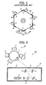
- the polygon mirror 120 of Figure 1 has a hexagonal planar shape and is rotated in a counterclockwise direction, which is in a direction indicated by arrow "X" shown in Figure 1.
- the polygon mirror 120 has a plurality of angled corners. Each angled corner includes upstream and downstream surfaces with respect to the rotation direction "X" of the polygon mirror 120.
- the downstream surface is represented by "A”
- the upstream surface is represented by "B.”
- a turbulent flow is generated due to a low pressure condition of air.
- the turbulent flow which is indicated by “TF” in Figure 1, can stir powder dust and fine particles that reside in the air in the optical writing unit.
- the stirred powder dust and fine particles collide or hit against the downstream surface "A" of the polygon mirror 120 and adhere to the polygon mirror 120.
- the collision of powder dust and fine particles to the polygon mirror 120 has contaminated the downstream surface of the polygon mirror 120.
- the contamination of the polygon mirror 120 has resulted in a decrease of reflectivity of the polygon mirror 120 and a deterioration of image quality.
- One of the techniques has included the following structure of an optical writing unit.
- the upstream surface "B" of the polygon mirror 120 is used instead of the downstream surface "A" when a synchronous detection is performed to control an exposure timing in a main scanning direction of the polygon mirror 120.
- the above-described operation is performed since the polygon mirror 120 or other polygon mirrors having a simple structure cannot easily remove contamination adhered thereto.
- the polygon mirror 120 needs to be cleaned or replaced. This has caused an increase of costs.
- a different one of the techniques has been proposed to electrically discharge the polygon mirror 120 so as to reduce or prevent contamination of the polygon mirror 120.
- At least one example embodiment of the present patent application provides an optical writing unit that includes a housing configured to include a plurality of optical elements, a polygon mirror configured to deflect a laser light beam, and a collecting member disposed in the vicinity of the polygon mirror and configured to collect dust in the housing.
- the collecting member included in the optical writing unit according to at least one example embodiment of the present patent application may include an electrostatically collecting member.
- the collecting member included in the optical writing unit according to at least one example embodiment of the present patent application may include an adhesive member.
- the collecting member included in the optical writing unit according to at least one example embodiment of the present patent application may be directly mounted on the housing.
- the collecting member included in the optical writing unit may be mounted on a cover detachably attached to the housing.
- the collecting member included in the optical writing unit may be mounted on a frame attached to one of the housing and a cover detachably attached to the housing.
- the collecting member and the frame included in the optical writing unit may be integrally molded.
- the collecting member included in the optical writing unit may be mounted with a gap with respect to one of the housing and the cover.
- the optical writing unit according to at least one example embodiment of the present patent application may further include a separator configured to divide an inside portion of the housing into two sections, and the collecting member included in the optical writing unit according to at least one example embodiment of the present patent application may be mounted on the separator.
- the polygon mirror and the plurality of optical elements included in the optical writing unit according to at least one example embodiment of the present patent application may be arranged in a same section in the housing.
- the housing included in the optical writing unit may include a box configured to accommodate the polygon mirror so that the polygon mirror is separated the plurality of optical elements.
- At least one example embodiment of the present patent application provides an image forming system that includes the above-described optical writing unit therein.
- spatially relative terms such as “beneath”, “below”, “lower”, “above”, “upper” and the like may be used herein for ease of description to describe one element or feature's relationship to another element(s) or feature(s) as illustrated in the figures. It will be understood that the spatially relative terms are intended to encompass different orientations of the device in use or operation in addition to the orientation depicted in the figures. For example, if the device in the figures is turned over, elements describes as “below” or “beneath” other elements or features would hen be oriented “above” the other elements or features. Thus, term such as “below” can encompass both an orientation of above and below. The device may be otherwise oriented (rotated 90 degrees or at other orientations) and the spatially relative descriptors herein interpreted accordingly.
- first, second, etc. may be used herein to described various elements, components, regions, layers and/or sections, it should be understood that these elements, components, regions, layer and/or sections should not be limited by these terms. These terms are used only to distinguish one element, component, region, layer or section from another region, layer or section. Thus, a first element, component, region, layer or section discussed below could be termed a second element, component, region, layer or section without departing from the teachings of the present invention.
- the laser printer 100 of Figure 2 may serve as an image forming apparatus and includes an image forming unit 30 and an optical writing unit 10.
- the image forming unit 30 may form a toner image and includes a photoconductive element 1, a charging unit 2, a developing unit 3, a transfer unit 4, and a cleaning unit 5.
- the optical writing unit 10 may emit a laser light beam to expose or irradiate the photoconductive element 1 of the image forming unit 30 to form an electrostatic latent image on a surface of the photoconductive element 1.
- the photoconductive element 1 receives the laser light beam and bears or carries a thus formed electrostatic latent image on the surface thereof.
- the photoconductive element 1 is rotated by a photoconductive element drive unit (not shown) in a counterclockwise direction, which is a direction indicated by an arrow in Figure 2.
- the charging unit 2 uniformly charges the surface of the photoconductive element 1.
- the developing unit 3 develops the electrostatic latent image formed on the surface of the photoconductive element 1 to a visible toner image.
- the transfer unit 4 is applied with a predetermined charge to transfer the toner image formed on the surface of the photoconductive element 1 onto a transfer member.
- the cleaning unit 5 removes residual toner form the surface of the photoconductive element 1.
- the optical writing unit 10 includes an optical housing 11 to accommodate a polygon mirror 12, and a plurality of optical elements such as a f-theta lens group 13, mirrors 14, 15, and 16, and a slit 17.
- the polygon mirror 12 is rotated by a polygon motor 18 (see Figure 3) to receive and deflect a laser light beam emitted from a semiconductor laser (not shown).
- the f-theta lens group 13 serves as a group of optical elements to receive and refract the laser light beam.
- the mirrors 14, 15, and 16 sequentially reflect the laser light beam from the f-theta lens group 13.
- the slit 17 serves as an exit aperture or opening mounted on the optical housing 11 so that the laser light beam can pass therethrough toward the photoconductive element 1.
- the charging unit 2 uniformly charges the surface of the photoconductive element 1.
- the optical writing unit 10 emits a laser light beam to form an electrostatic latent image on the surface of the photoconductive element 1.
- the developing unit 3 then develops the electrostatic latent image on the photoconductive element 1 to a visible toner image.
- a sheet feeding unit (not shown) provided in the laser printer 100 feeds and conveys a transfer sheet (not shown).
- the transfer unit 4 causes the toner image formed on the photoconductive element 1 to be transferred onto a surface of the transfer sheet.
- the toner image is fixed to the transfer sheet by a fixing unit (not shown) and is discharged to the outside of the laser printer 100.
- the cleaning unit 5 removes residual toner remaining on the surface of the photoconductive element 1.
- the polygon motor 18 drives the polygon mirror 12.
- a semiconductor laser (not shown) launches a laser light beam.
- the launched laser light beam passes through a collimator lens (not shown), a spherical lens (not shown), and a cylindrical lens (not shown), and reaches the polygon mirror 12.
- the incident laser light beam is deflected by the polygon mirror 12, passes through the f-theta lens group 13, and is sequentially reflected by the mirrors 14, 15, and 16. After being reflected by the mirror 16, the laser light beam passes through the slit 17 in an obliquely upward direction to the outside of the optical writing unit 10 toward the photoconductive element 1. Then, the laser light beam is collected to the photoconductive element 1 so as to scan the surface of the photoconductive element 1 in its axial direction.
- the polygon mirror 12 may not be contaminated. It is, however, difficult or impossible to block or remove dust and particles from the optical housing 11 at the manufacturing stage. It is also difficult to form the optical housing 11 of the optical writing unit 10 in a closed shape that can completely shut out such dust and particles therefrom.
- the optical writing unit 10 further includes a collecting member 20.
- the collecting member 20 may be directly mounted onto a top surface of the optical housing 11 of the optical writing unit 10, which is located in the vicinity of and over the polygon mirror 12.
- the collecting member 20 may collect powder dust and fine particles that reside in the optical housing 11 of the optical writing unit 10 so that contamination on the polygon mirror 12 can be reduced or prevented.
- the collecting member 20 may be formed with a member that can collect and firmly keep dust and fine particles from leaving.
- the collecting member 20 includes an electrostatically collecting member that is charged and electrostatically attract powder dust and fine particles or includes an adhesive member that causes dust and fine particles to be adhered thereto.
- the optical writing unit 10 further includes an electrostatically collecting filter 20f that serves as the collecting member 20.
- the electrostatically collecting filter 20f may have permeability to air and be electrically charged.
- the electrostatically collecting filter 20f or the collecting member 20 in Figure 4 may indirectly be mounted on the optical housing 11 of the optical writing unit 10. Specifically, the electrostatically collecting filter 20f may be mounted on a frame 21, which is supported by legs 23 that are attached to the optical housing 11 of the optical writing unit 10. The electrostatically collecting filter 20f may be located in the vicinity of and over the polygon mirror 12 as the collecting member 20 of Figure 3.
- the electrostatically collecting member 20f with the above-described structure may also collect powder dust and fine particles that reside in the optical housing 11 of the optical writing unit 10 so that contamination on the polygon mirror 12 can be reduced or prevented.
- the frame 21 may include a plurality of openings 22 to let air through, as shown in Figure 5.
- the electrostatically collecting filter 20f may be mounted so as to cover the plurality of openings 22 of the frame 21.
- the frame 21 and the electrostatically collecting filter 20f may be integrally molded. This can skip one step in the manufacturing stage for attaching the electrostatically collecting filter 20f to the frame 21, which can greatly contribute to a significant cost reduction.
- the air in the optical housing 11 of the optical writing unit 10 may flow in the direction "D", and powder dust and fine particles may be conveyed by the air that flows in the direction "D.”
- the electrostatically collecting filter 20f attached to the frame 21 that is mounted on the optical housing 11, the powder dust and fine particles may be collected thereby.
- the collection of dust by the electrostatically collecting filter 20f serving as the collecting member 20 can reduce a great amount of powder dust and fine particles that collide against and adhere to a plurality of surfaces of the polygon mirror 12. Similar to the collecting member 20 provided to the structure shown in Figure 3, the electrostatically collecting filter 20f provided to the structure shown in Figure 4 may effectively reduce or prevent a contamination of the polygon mirror 12.
- the electrostatically collecting filter 20f is mounted on the top surface or a ceiling of the optical housing 11 provided with a predetermined gap therebetween.
- the optical housing 11 can have a structure in which the electrostatically collecting filter 20f shown in Figure 4 can be directly mounted on the top surface of the optical housing 11.
- the electrostatically collecting filter 20f can be mounted on a different surface, instead of the top surface, of the optical housing 11, directly or with a predetermined gap therebetween.
- the collecting member 20 including the electrostatically collecting filter 20f can be mounted on a cover (not shown) that may detachably be attached to the optical housing 11 of the optical writing unit 10. With the above-described structure, the collecting member 20 including the electrostatically collecting filter 20f can easily be cleaned or replaced.
- the structures shown in Figures 3 and 4 have one section in the optical housing 11. That is, an inside portion of the optical housing 11 is not divided, thereby the polygon mirror 12 with other optical elements are accommodated in the same section in the inside portion.
- the optical housing 11 of the optical writing unit 10 may have a structure as shown in Figure 6.
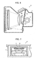
- the optical housing 11 is separated or divided by a separation plate 24, which serves as a separator, into two sections. That is, one section may accommodate the polygon mirror 12 and the polygon motor 18 (not shown in Figure 6), and the other section may accommodate the other optical elements provided in the optical writing unit 10.
- optical housing 11 of the optical writing unit 10 may have structures as shown in Figures 7 and 8 so that the polygon mirror 12 can be sufficiently closed in a box 25.
- Both the collecting member 20 and the electrostatically collecting filter 20f according to at least one example embodiment of the present patent application can be applied to each type of the optical writing unit 10.
- the collecting member 20 including the electrostatically collecting filter 20f may be mounted on a surface of the separation plate 24 other than a transparent portion (not shown) through which the laser light beam may pass.
- the optical writing unit 10 having the structures shown in Figures 7 and 8 may include the polygon mirror 12 in the box 25 in the optical housing 11 so as to separate the polygon mirror 12 from other optical elements.
- the polygon mirror 12 may be placed and covered in a small space by the box 25, and the collecting member 20 including the electrostatically collecting filter 20f may be mounted in the box 25.
- the collecting member 20 including the electrostatically collecting filter 20f may be mounted in the box 25.
Landscapes
- Physics & Mathematics (AREA)
- General Physics & Mathematics (AREA)
- Optics & Photonics (AREA)
- Facsimile Scanning Arrangements (AREA)
- Laser Beam Printer (AREA)
- Mechanical Optical Scanning Systems (AREA)
- Control Or Security For Electrophotography (AREA)
Abstract
Description
- The present patent application relates to an optical writing unit and an image forming apparatus including the optical writing unit therein.
- Related art image forming apparatuses, such as laser printers and digital copiers, generally include an optical writing unit. The optical writing unit includes a housing that accommodates a plurality of optical elements and a polygon mirror that deflects a laser light beam.
- Referring to Figure 1, a
polygon mirror 120 used in an optical writing unit of a related art image forming apparatus is described. - The
polygon mirror 120 of Figure 1 has a hexagonal planar shape and is rotated in a counterclockwise direction, which is in a direction indicated by arrow "X" shown in Figure 1. Thepolygon mirror 120 has a plurality of angled corners. Each angled corner includes upstream and downstream surfaces with respect to the rotation direction "X" of thepolygon mirror 120. In Figure 1, the downstream surface is represented by "A", and the upstream surface is represented by "B." - When the
polygon mirror 120 is rotated in the direction indicated by arrow "X" as shown in Figure 1, a turbulent flow is generated due to a low pressure condition of air. The turbulent flow, which is indicated by "TF" in Figure 1, can stir powder dust and fine particles that reside in the air in the optical writing unit. The stirred powder dust and fine particles collide or hit against the downstream surface "A" of thepolygon mirror 120 and adhere to thepolygon mirror 120. The collision of powder dust and fine particles to thepolygon mirror 120 has contaminated the downstream surface of thepolygon mirror 120. The contamination of thepolygon mirror 120 has resulted in a decrease of reflectivity of thepolygon mirror 120 and a deterioration of image quality. - To reduce the above-described disadvantages, some techniques have been used.
- One of the techniques has included the following structure of an optical writing unit. In the optical writing unit, the upstream surface "B" of the
polygon mirror 120 is used instead of the downstream surface "A" when a synchronous detection is performed to control an exposure timing in a main scanning direction of thepolygon mirror 120. The above-described operation is performed since thepolygon mirror 120 or other polygon mirrors having a simple structure cannot easily remove contamination adhered thereto. - However, once the quality of images is deteriorated, the
polygon mirror 120 needs to be cleaned or replaced. This has caused an increase of costs. - A different one of the techniques has been proposed to electrically discharge the
polygon mirror 120 so as to reduce or prevent contamination of thepolygon mirror 120. - However, the discharge of electric charge from the
polygon mirror 120 has not sufficiently removed the contamination caused by the turbulent flow. - One of more embodiments of the present patent application has been made, taking the above-mentioned circumstances into consideration.
- At least one example embodiment of the present patent application provides an optical writing unit that includes a housing configured to include a plurality of optical elements, a polygon mirror configured to deflect a laser light beam, and a collecting member disposed in the vicinity of the polygon mirror and configured to collect dust in the housing.
- The collecting member included in the optical writing unit according to at least one example embodiment of the present patent application may include an electrostatically collecting member.
- The collecting member included in the optical writing unit according to at least one example embodiment of the present patent application may include an adhesive member.
- The collecting member included in the optical writing unit according to at least one example embodiment of the present patent application may be directly mounted on the housing.
- The collecting member included in the optical writing unit according to at least one example embodiment of the present patent application may be mounted on a cover detachably attached to the housing.
- The collecting member included in the optical writing unit according to at least one example embodiment of the present patent application may be mounted on a frame attached to one of the housing and a cover detachably attached to the housing.
- The collecting member and the frame included in the optical writing unit according to at least one example embodiment of the present patent application may be integrally molded.
- The collecting member included in the optical writing unit according to at least one example embodiment of the present patent application may be mounted with a gap with respect to one of the housing and the cover.
- The optical writing unit according to at least one example embodiment of the present patent application may further include a separator configured to divide an inside portion of the housing into two sections, and the collecting member included in the optical writing unit according to at least one example embodiment of the present patent application may be mounted on the separator.
- The polygon mirror and the plurality of optical elements included in the optical writing unit according to at least one example embodiment of the present patent application may be arranged in a same section in the housing.
- The housing included in the optical writing unit according to at least one example embodiment of the present patent application may include a box configured to accommodate the polygon mirror so that the polygon mirror is separated the plurality of optical elements.
- At least one example embodiment of the present patent application provides an image forming system that includes the above-described optical writing unit therein.
- The accompanying drawings are intended to depict example embodiments of the present invention and should not be interpreted to limit the scope thereof. The accompanying drawings are not to be considered as drawn to scale unless explicitly noted.
- A more complete appreciation of the disclosure and many of the attendant advantages thereof will be readily obtained as the same becomes better understood by reference to the following detailed description when considered in connection with the accompanying drawings, wherein:
- Figure 1 is a background structure of a polygon mirror;
- Figure 2 is a schematic structure of a laser printer as at least one example embodiment of the present patent application;
- Figure 3 is a schematic structure of an optical writing unit, included in the laser printer of Figure 2, according to the at least one example embodiment of the present patent application;
- Figure 4 is a schematic structure of a different example of the optical writing unit according to the at least one example embodiment of the present patent application;
- Figure 5 is a structure of a frame and a collecting member provided to the optical writing unit according to the at least one example embodiment of the present invention;
- Figure 6 is a schematic structure of a different example of the optical writing unit according to the at least one example embodiment of the present patent application;
- Figure 7 is a schematic structure of a different example of the optical writing unit according to the at least one example embodiment of the present patent application; and
- Figure 8 is a schematic structure of a different example of the optical writing unit according to the at least one example embodiment of the present patent application.
- It will be understood that if an element or layer is referred to as being "on", "against", "connected to" or "coupled to" another element or layer, then it can be directly on, against, connected or coupled to the other element or layer, or intervening elements or layers may be present. In contrast, if an element is referred to as being "directly on", "directly connected to" or "directly coupled to" another element or layer, then there are no intervening elements or layers present. Like numbers referred to like elements throughout. As used herein, the term "and/or" includes any and all combinations of one or more of the associated listed items.
- Spatially relative terms, such as "beneath", "below", "lower", "above", "upper" and the like may be used herein for ease of description to describe one element or feature's relationship to another element(s) or feature(s) as illustrated in the figures. It will be understood that the spatially relative terms are intended to encompass different orientations of the device in use or operation in addition to the orientation depicted in the figures. For example, if the device in the figures is turned over, elements describes as "below" or "beneath" other elements or features would hen be oriented "above" the other elements or features. Thus, term such as "below" can encompass both an orientation of above and below. The device may be otherwise oriented (rotated 90 degrees or at other orientations) and the spatially relative descriptors herein interpreted accordingly.
- Although the terms first, second, etc. may be used herein to described various elements, components, regions, layers and/or sections, it should be understood that these elements, components, regions, layer and/or sections should not be limited by these terms. These terms are used only to distinguish one element, component, region, layer or section from another region, layer or section. Thus, a first element, component, region, layer or section discussed below could be termed a second element, component, region, layer or section without departing from the teachings of the present invention.
- The terminology used herein is for the purpose of describing particular embodiments only and is not intended to be limiting of the present invention. As used herein, the singular forms "a", "an" and "the" are intended to include the plural forms as well, unless the context clearly indicates otherwise. It will be further understood that the terms "includes" and/or "including", when used in this specification, specify the presence of stated features, integers, steps, operations, elements, and/or components, but do not preclude the presence or addition of one or more other features, integers, steps, operations, elements, components, and/or groups thereof.
- In describing example embodiments illustrated in the drawings, specific terminology is employed for the sake of clarity. However, the disclosure of this patent specification is not intended to be limited to the specific terminology so selected and it is to be understood that each specific element includes all technical equivalents that operate in a similar manner.
- Referring now to the drawings, wherein like reference numerals designate identical or corresponding parts throughout the several views, example embodiments of the present patent application are described.
- Referring to Figure 2, a schematic structure of a
laser printer 100 according to an example embodiment of the present patent application is described. - The
laser printer 100 of Figure 2 may serve as an image forming apparatus and includes animage forming unit 30 and anoptical writing unit 10. - The
image forming unit 30 may form a toner image and includes aphotoconductive element 1, a chargingunit 2, a developingunit 3, a transfer unit 4, and acleaning unit 5. - The
optical writing unit 10 may emit a laser light beam to expose or irradiate thephotoconductive element 1 of theimage forming unit 30 to form an electrostatic latent image on a surface of thephotoconductive element 1. - As described above, the
photoconductive element 1 receives the laser light beam and bears or carries a thus formed electrostatic latent image on the surface thereof. Thephotoconductive element 1 is rotated by a photoconductive element drive unit (not shown) in a counterclockwise direction, which is a direction indicated by an arrow in Figure 2. - The charging
unit 2 uniformly charges the surface of thephotoconductive element 1. - The developing
unit 3 develops the electrostatic latent image formed on the surface of thephotoconductive element 1 to a visible toner image. - The transfer unit 4 is applied with a predetermined charge to transfer the toner image formed on the surface of the
photoconductive element 1 onto a transfer member. - The
cleaning unit 5 removes residual toner form the surface of thephotoconductive element 1. - The
optical writing unit 10 includes anoptical housing 11 to accommodate apolygon mirror 12, and a plurality of optical elements such as a f-theta lens group 13, mirrors 14, 15, and 16, and aslit 17. - The
polygon mirror 12 is rotated by a polygon motor 18 (see Figure 3) to receive and deflect a laser light beam emitted from a semiconductor laser (not shown). - The f-
theta lens group 13 serves as a group of optical elements to receive and refract the laser light beam. - The
mirrors theta lens group 13. - The
slit 17 serves as an exit aperture or opening mounted on theoptical housing 11 so that the laser light beam can pass therethrough toward thephotoconductive element 1. - Operations of the
laser printer 100 are described. - When the photoconductive element drive unit starts to rotate the
photoconductive element 1, the chargingunit 2 uniformly charges the surface of thephotoconductive element 1. Theoptical writing unit 10 emits a laser light beam to form an electrostatic latent image on the surface of thephotoconductive element 1. The developingunit 3 then develops the electrostatic latent image on thephotoconductive element 1 to a visible toner image. - At the same time, a sheet feeding unit (not shown) provided in the
laser printer 100 feeds and conveys a transfer sheet (not shown). When the transfer sheet is conveyed to thephotoconductive element 1, the transfer unit 4 causes the toner image formed on thephotoconductive element 1 to be transferred onto a surface of the transfer sheet. The toner image is fixed to the transfer sheet by a fixing unit (not shown) and is discharged to the outside of thelaser printer 100. - After the toner image has been transferred onto the transfer sheet, the
cleaning unit 5 removes residual toner remaining on the surface of thephotoconductive element 1. - Detailed operations of the
optical writing unit 10 are now described. - The
polygon motor 18 drives thepolygon mirror 12. A semiconductor laser (not shown) launches a laser light beam. The launched laser light beam passes through a collimator lens (not shown), a spherical lens (not shown), and a cylindrical lens (not shown), and reaches thepolygon mirror 12. - The incident laser light beam is deflected by the
polygon mirror 12, passes through the f-theta lens group 13, and is sequentially reflected by themirrors mirror 16, the laser light beam passes through theslit 17 in an obliquely upward direction to the outside of theoptical writing unit 10 toward thephotoconductive element 1. Then, the laser light beam is collected to thephotoconductive element 1 so as to scan the surface of thephotoconductive element 1 in its axial direction. - When the
polygon mirror 12 is rotated in the above-described structure of Figure 2, a turbulent flow may occur in theoptical writing unit 10, which may cause powder dust and fine particles to stir up in theoptical writing unit 10 and to contaminate predetermined surfaces of thepolygon mirror 12. - If dust does not enter and reside in the
optical housing 11 of theoptical writing unit 10, thepolygon mirror 12 may not be contaminated. It is, however, difficult or impossible to block or remove dust and particles from theoptical housing 11 at the manufacturing stage. It is also difficult to form theoptical housing 11 of theoptical writing unit 10 in a closed shape that can completely shut out such dust and particles therefrom. - Referring to Figures 3 and 4, schematic structures of the
optical writing unit 10 according to example embodiments of the present patent application are described. - In Figure 3, the
optical writing unit 10 further includes a collectingmember 20. - The collecting
member 20 may be directly mounted onto a top surface of theoptical housing 11 of theoptical writing unit 10, which is located in the vicinity of and over thepolygon mirror 12. - The collecting
member 20 may collect powder dust and fine particles that reside in theoptical housing 11 of theoptical writing unit 10 so that contamination on thepolygon mirror 12 can be reduced or prevented. - When the
polygon mirror 12 is rotated in theoptical writing unit 10 having the structure shown in Figure 3, air in theoptical housing 11 of theoptical writing unit 10 may flow in a direction as indicated by arrow "C." Such powder dust and fine particles may be conveyed by the air that flows in the direction "C" and be collected by the collectingmember 20. The collection of powder dust and fine particles by the collectingmember 20 can reduce a great amount of powder dust and fine particles that collide against and adhere to a plurality of surfaces of thepolygon mirror 12. This may effectively reduce or prevent a contamination of thepolygon mirror 12. - The collecting
member 20 may be formed with a member that can collect and firmly keep dust and fine particles from leaving. For example, it is preferable the collectingmember 20 includes an electrostatically collecting member that is charged and electrostatically attract powder dust and fine particles or includes an adhesive member that causes dust and fine particles to be adhered thereto. - In Figure 4, the
optical writing unit 10 further includes an electrostatically collectingfilter 20f that serves as the collectingmember 20. The electrostatically collectingfilter 20f may have permeability to air and be electrically charged. - The electrostatically collecting
filter 20f or the collectingmember 20 in Figure 4 may indirectly be mounted on theoptical housing 11 of theoptical writing unit 10. Specifically, the electrostatically collectingfilter 20f may be mounted on aframe 21, which is supported bylegs 23 that are attached to theoptical housing 11 of theoptical writing unit 10. The electrostatically collectingfilter 20f may be located in the vicinity of and over thepolygon mirror 12 as the collectingmember 20 of Figure 3. - The electrostatically collecting
member 20f with the above-described structure may also collect powder dust and fine particles that reside in theoptical housing 11 of theoptical writing unit 10 so that contamination on thepolygon mirror 12 can be reduced or prevented. - When the
polygon mirror 12 is rotated in theoptical writing unit 10 having the structure shown in Figure 4, air in theoptical housing 11 of theoptical writing unit 10 may flow in a direction as indicated by arrow "D." As the air passes through the electrostatically collectingfilter 20f, the powder dust and fine particles may be collected thereby. - Referring to Figure 5, a structure of the
frame 21 of Figure 4 is described. - The
frame 21 may include a plurality ofopenings 22 to let air through, as shown in Figure 5. The electrostatically collectingfilter 20f may be mounted so as to cover the plurality ofopenings 22 of theframe 21. - The
frame 21 and the electrostatically collectingfilter 20f may be integrally molded. This can skip one step in the manufacturing stage for attaching the electrostatically collectingfilter 20f to theframe 21, which can greatly contribute to a significant cost reduction. - As previously described, the air in the
optical housing 11 of theoptical writing unit 10 may flow in the direction "D", and powder dust and fine particles may be conveyed by the air that flows in the direction "D." As the air passes through the electrostatically collectingfilter 20f attached to theframe 21 that is mounted on theoptical housing 11, the powder dust and fine particles may be collected thereby. The collection of dust by theelectrostatically collecting filter 20f serving as the collectingmember 20 can reduce a great amount of powder dust and fine particles that collide against and adhere to a plurality of surfaces of thepolygon mirror 12. Similar to the collectingmember 20 provided to the structure shown in Figure 3, the electrostatically collectingfilter 20f provided to the structure shown in Figure 4 may effectively reduce or prevent a contamination of thepolygon mirror 12. - In the example embodiment of the present patent application, the electrostatically collecting
filter 20f is mounted on the top surface or a ceiling of theoptical housing 11 provided with a predetermined gap therebetween. However, similar to the collectingmember 20 shown in Figure 3, theoptical housing 11 can have a structure in which the electrostatically collectingfilter 20f shown in Figure 4 can be directly mounted on the top surface of theoptical housing 11. - Further, the electrostatically collecting
filter 20f can be mounted on a different surface, instead of the top surface, of theoptical housing 11, directly or with a predetermined gap therebetween. - Further, the collecting
member 20 including the electrostatically collectingfilter 20f can be mounted on a cover (not shown) that may detachably be attached to theoptical housing 11 of theoptical writing unit 10. With the above-described structure, the collectingmember 20 including the electrostatically collectingfilter 20f can easily be cleaned or replaced. - Referring now to Figures 6, 7, and 8, alternative structures of the
optical writing unit 10 according to at least one example embodiment of the present patent application are described. - There are various types of structures for the
optical writing unit 10. For example, the structures shown in Figures 3 and 4 have one section in theoptical housing 11. That is, an inside portion of theoptical housing 11 is not divided, thereby thepolygon mirror 12 with other optical elements are accommodated in the same section in the inside portion. - On the other hand, the
optical housing 11 of theoptical writing unit 10 may have a structure as shown in Figure 6. In theoptical writing unit 10 shown in Figure 6, theoptical housing 11 is separated or divided by aseparation plate 24, which serves as a separator, into two sections. That is, one section may accommodate thepolygon mirror 12 and the polygon motor 18 (not shown in Figure 6), and the other section may accommodate the other optical elements provided in theoptical writing unit 10. - Further, the
optical housing 11 of theoptical writing unit 10 may have structures as shown in Figures 7 and 8 so that thepolygon mirror 12 can be sufficiently closed in abox 25. - Both the collecting
member 20 and the electrostatically collectingfilter 20f according to at least one example embodiment of the present patent application can be applied to each type of theoptical writing unit 10. - Further, in the
optical writing unit 10 having the structure shown in Figure 6, the collectingmember 20 including the electrostatically collectingfilter 20f may be mounted on a surface of theseparation plate 24 other than a transparent portion (not shown) through which the laser light beam may pass. - As previously described, the
optical writing unit 10 having the structures shown in Figures 7 and 8 may include thepolygon mirror 12 in thebox 25 in theoptical housing 11 so as to separate thepolygon mirror 12 from other optical elements. In the above-described structure, thepolygon mirror 12 may be placed and covered in a small space by thebox 25, and the collectingmember 20 including the electrostatically collectingfilter 20f may be mounted in thebox 25. With the above-described structure, powder dust and fine particles that reside in thebox 25 can surely be collected. Thereby, the contamination of thepolygon mirror 12 can more effectively be reduced or prevented. - The above-described example embodiments are illustrative, and numerous additional modifications and variations are possible in light of the above teachings. For example, elements and/or features of different example embodiments herein may be combined with each other and/or substituted for each other within the scope of this disclosure and appended claims. It is therefore to be understood that within the scope of the appended claims, the disclosure of this patent specification may be practiced otherwise than as specifically described herein.
- This patent application is based on
Japanese patent application no. 2005-363142
Claims (12)
- An optical writing unit, comprising:a housing configured to includea plurality of optical elements;a polygon mirror configured to deflect a laser light beam; anda collecting member disposed in the vicinity of the polygon mirror and configured to collect dust in the housing.
- The optical writing unit according to claim 1, wherein:the collecting member includes an electrostatically collecting member.
- The optical writing unit according to claim 1, wherein:the collecting member includes an adhesive member.
- The optical writing unit according to claim 1, wherein:the collecting member is directly mounted on the housing.
- The optical writing unit according to claim 1, wherein:the collecting member is mounted on a cover detachably attached to the housing.
- The optical writing unit according to claim 1, wherein:the collecting member is mounted on a frame attached to one of the housing and a cover detachably attached to the housing.
- The optical writing unit according to claim 6, wherein:the collecting member and the frame are integrally molded.
- The optical writing unit according to claim 6, wherein:the collecting member is mounted with a gap with respect to one of the housing and the cover.
- The optical writing unit according to claim 1, further comprising:a separator configured to divide an inside portion of the housing into two sections, andthe collecting member is mounted on the separator.
- The optical writing unit according to claim 1, wherein:the polygon mirror and the plurality of optical elements are arranged in a same section in the housing.
- The optical writing unit according to claim 1, wherein:the housing includes a box configured to accommodate the polygon mirror so that the polygon mirror is separated from the plurality of optical elements.
- An image forming apparatus, comprising:an image bearing member; and the optical unit of one of claims 1 to 11, wherein theplurality of optical elements are for exposing the image bearing member.
Applications Claiming Priority (1)
| Application Number | Priority Date | Filing Date | Title |
|---|---|---|---|
| JP2005363142A JP4669780B2 (en) | 2005-12-16 | 2005-12-16 | Optical scanning apparatus and image forming apparatus |
Publications (2)
| Publication Number | Publication Date |
|---|---|
| EP1798586A1 true EP1798586A1 (en) | 2007-06-20 |
| EP1798586B1 EP1798586B1 (en) | 2011-02-16 |
Family
ID=37875691
Family Applications (1)
| Application Number | Title | Priority Date | Filing Date |
|---|---|---|---|
| EP06025821A Ceased EP1798586B1 (en) | 2005-12-16 | 2006-12-13 | An optical writing unit and a image forming apparatus including the same |
Country Status (5)
| Country | Link |
|---|---|
| US (1) | US7667726B2 (en) |
| EP (1) | EP1798586B1 (en) |
| JP (1) | JP4669780B2 (en) |
| CN (1) | CN100487518C (en) |
| DE (1) | DE602006020105D1 (en) |
Families Citing this family (16)
| Publication number | Priority date | Publication date | Assignee | Title |
|---|---|---|---|---|
| US7473301B2 (en) * | 2002-09-17 | 2009-01-06 | Euv Llc | Adhesive particle shielding |
| JP5145651B2 (en) * | 2006-04-27 | 2013-02-20 | 株式会社リコー | Optical scanning apparatus and image forming apparatus |
| JP2008216438A (en) * | 2007-03-01 | 2008-09-18 | Ricoh Co Ltd | Optical scanning apparatus and image forming apparatus |
| JP5016997B2 (en) * | 2007-07-02 | 2012-09-05 | 株式会社リコー | Optical scanning apparatus and image forming apparatus |
| JP4887268B2 (en) * | 2007-12-13 | 2012-02-29 | 株式会社リコー | Curvature correction mechanism, optical scanning device, and image forming apparatus |
| JP5240576B2 (en) * | 2009-06-19 | 2013-07-17 | 株式会社リコー | Optical scanning apparatus and image forming apparatus |
| JP5637494B2 (en) * | 2010-08-20 | 2014-12-10 | 株式会社リコー | Optical scanning apparatus and image forming apparatus |
| JP5472009B2 (en) * | 2010-09-27 | 2014-04-16 | 株式会社リコー | Optical deflector, optical scanning device, and image forming apparatus |
| JP5903894B2 (en) | 2012-01-06 | 2016-04-13 | 株式会社リコー | Optical scanning apparatus and image forming apparatus |
| JP2013167676A (en) | 2012-02-14 | 2013-08-29 | Kyocera Document Solutions Inc | Image forming apparatus |
| JP6435805B2 (en) | 2014-11-20 | 2018-12-12 | 株式会社リコー | Housing structure, optical scanning device, and image forming apparatus |
| JP6520174B2 (en) | 2015-02-10 | 2019-05-29 | 株式会社リコー | Housing structure, optical scanning device and image forming apparatus |
| CN109416467B (en) | 2016-08-22 | 2021-04-09 | 京瓷办公信息系统株式会社 | Optical scanning device and image forming apparatus having the same |
| US10942468B2 (en) | 2016-10-24 | 2021-03-09 | Kyocera Document Solutions Inc. | Optical scanning device and image forming apparatus including the same |
| JP6926761B2 (en) * | 2017-07-18 | 2021-08-25 | セイコーエプソン株式会社 | Optical modules and electronic devices |
| US12088765B2 (en) | 2022-03-22 | 2024-09-10 | Ricoh Company, Ltd. | Casing structure, optical scanner, and image forming apparatus |
Citations (5)
| Publication number | Priority date | Publication date | Assignee | Title |
|---|---|---|---|---|
| JPH11183836A (en) * | 1997-12-24 | 1999-07-09 | Canon Inc | Optical scanning device |
| JPH11281909A (en) * | 1998-03-31 | 1999-10-15 | Sankyo Seiki Mfg Co Ltd | Optical scanner |
| JP2000356753A (en) * | 1999-06-15 | 2000-12-26 | Kyocera Corp | Scanning optical device |
| US6339491B1 (en) * | 1998-12-09 | 2002-01-15 | Fuji Photo Film Co., Ltd. | Dustproof structure of optical box |
| JP2003167110A (en) * | 2001-11-30 | 2003-06-13 | Hitachi Printing Solutions Ltd | Polygon mirror with dust collecting function and protective film |
Family Cites Families (20)
| Publication number | Priority date | Publication date | Assignee | Title |
|---|---|---|---|---|
| EP0080728B1 (en) * | 1981-11-30 | 1986-04-23 | Hitachi, Ltd. | Light beam printer |
| JPH0569720U (en) * | 1992-02-20 | 1993-09-21 | 株式会社ジャパンイメージングシステム | Optical box |
| JP3308991B2 (en) * | 1992-07-31 | 2002-07-29 | 株式会社リコー | Data transfer device |
| JPH06148550A (en) * | 1992-11-10 | 1994-05-27 | Canon Inc | Optical scanning device |
| JPH0862528A (en) * | 1994-08-25 | 1996-03-08 | Canon Inc | Optical scanning device |
| JPH103054A (en) * | 1996-06-17 | 1998-01-06 | Canon Inc | Deflection scanning device |
| JPH10250145A (en) * | 1997-03-14 | 1998-09-22 | Ricoh Co Ltd | Image forming device |
| JPH11218710A (en) | 1998-02-04 | 1999-08-10 | Canon Inc | Scanning optical device |
| JPH11227249A (en) * | 1998-02-16 | 1999-08-24 | Ricoh Co Ltd | Image forming apparatus |
| JPH11264949A (en) * | 1998-03-16 | 1999-09-28 | Canon Inc | Optical deflector |
| JP3668022B2 (en) * | 1998-11-16 | 2005-07-06 | 株式会社リコー | Image forming apparatus |
| US6593951B2 (en) * | 2000-09-25 | 2003-07-15 | Ricoh Company, Ltd. | Optical writing system directed to miniaturization thereof, and image forming apparatus employing it |
| JP3652238B2 (en) | 2000-11-29 | 2005-05-25 | シャープ株式会社 | Optical scanning optical device |
| JP2002214558A (en) | 2001-01-23 | 2002-07-31 | Ricoh Co Ltd | Polygon unit cooling structure |
| JP4386325B2 (en) * | 2001-09-21 | 2009-12-16 | 株式会社リコー | Image forming apparatus |
| JP4008262B2 (en) * | 2002-02-28 | 2007-11-14 | 株式会社リコー | Image forming apparatus |
| JP4318280B2 (en) * | 2002-04-17 | 2009-08-19 | 株式会社リコー | Image reading device |
| JP2004354848A (en) * | 2003-05-30 | 2004-12-16 | Ricoh Co Ltd | Optical scanning device and image forming apparatus |
| JP4225838B2 (en) * | 2003-06-03 | 2009-02-18 | 株式会社リコー | Laser writing apparatus and image forming apparatus |
| JP4584789B2 (en) * | 2005-03-16 | 2010-11-24 | 株式会社リコー | Optical scanning apparatus and image forming apparatus |
-
2005
- 2005-12-16 JP JP2005363142A patent/JP4669780B2/en not_active Expired - Fee Related
-
2006
- 2006-12-13 DE DE602006020105T patent/DE602006020105D1/en active Active
- 2006-12-13 EP EP06025821A patent/EP1798586B1/en not_active Ceased
- 2006-12-14 CN CNB2006101694994A patent/CN100487518C/en not_active Expired - Fee Related
- 2006-12-15 US US11/639,417 patent/US7667726B2/en not_active Expired - Fee Related
Patent Citations (5)
| Publication number | Priority date | Publication date | Assignee | Title |
|---|---|---|---|---|
| JPH11183836A (en) * | 1997-12-24 | 1999-07-09 | Canon Inc | Optical scanning device |
| JPH11281909A (en) * | 1998-03-31 | 1999-10-15 | Sankyo Seiki Mfg Co Ltd | Optical scanner |
| US6339491B1 (en) * | 1998-12-09 | 2002-01-15 | Fuji Photo Film Co., Ltd. | Dustproof structure of optical box |
| JP2000356753A (en) * | 1999-06-15 | 2000-12-26 | Kyocera Corp | Scanning optical device |
| JP2003167110A (en) * | 2001-11-30 | 2003-06-13 | Hitachi Printing Solutions Ltd | Polygon mirror with dust collecting function and protective film |
Also Published As
| Publication number | Publication date |
|---|---|
| CN100487518C (en) | 2009-05-13 |
| JP4669780B2 (en) | 2011-04-13 |
| US20070139745A1 (en) | 2007-06-21 |
| JP2007164048A (en) | 2007-06-28 |
| US7667726B2 (en) | 2010-02-23 |
| EP1798586B1 (en) | 2011-02-16 |
| DE602006020105D1 (en) | 2011-03-31 |
| CN1982941A (en) | 2007-06-20 |
Similar Documents
| Publication | Publication Date | Title |
|---|---|---|
| EP1798586B1 (en) | An optical writing unit and a image forming apparatus including the same | |
| US7414239B2 (en) | Optical-scanning apparatus and image forming apparatus | |
| EP1462867A1 (en) | Cover with cleaning member for opening of optical writing device, and image forming apparatus and method using said device | |
| EP3712707B1 (en) | Developing device, process cartridge, and image forming apparatus | |
| CN103529677A (en) | Image forming apparatus | |
| JP2006146117A (en) | Image forming apparatus | |
| JPH11183836A (en) | Optical scanning device | |
| JP2010250115A (en) | Optical scanner and image-forming device | |
| JP3928475B2 (en) | Reading apparatus and image forming apparatus | |
| JPH0545945A (en) | Electrophotographic image forming apparatus | |
| JP7206614B2 (en) | Developing device and image forming device | |
| US9558431B2 (en) | Optical scanning apparatus | |
| JP2004271864A (en) | Image forming device | |
| JP5157996B2 (en) | Optical deflector, optical scanning device, and image forming apparatus | |
| JPS62194261A (en) | Light beam printer | |
| JP4613880B2 (en) | Image recording device | |
| JP3676114B2 (en) | Optical deflector | |
| JP5145651B2 (en) | Optical scanning apparatus and image forming apparatus | |
| JP6964510B2 (en) | Optical scanning device and image forming device | |
| CN109313338B (en) | Optical scanning device and image forming apparatus having the same | |
| JPH0252263B2 (en) | ||
| JP2005164731A (en) | Image forming apparatus | |
| JP2002271568A (en) | Image forming device | |
| JP2020126132A (en) | Optical scanning device, method of manufacturing optical scanning device, and image forming apparatus including optical scanning device | |
| JPH03200166A (en) | Optical device |
Legal Events
| Date | Code | Title | Description |
|---|---|---|---|
| PUAI | Public reference made under article 153(3) epc to a published international application that has entered the european phase |
Free format text: ORIGINAL CODE: 0009012 |
|
| AK | Designated contracting states |
Kind code of ref document: A1 Designated state(s): AT BE BG CH CY CZ DE DK EE ES FI FR GB GR HU IE IS IT LI LT LU LV MC NL PL PT RO SE SI SK TR |
|
| AX | Request for extension of the european patent |
Extension state: AL BA HR MK YU |
|
| 17P | Request for examination filed |
Effective date: 20070831 |
|
| AKX | Designation fees paid |
Designated state(s): DE ES FR GB IT |
|
| 17Q | First examination report despatched |
Effective date: 20090120 |
|
| GRAP | Despatch of communication of intention to grant a patent |
Free format text: ORIGINAL CODE: EPIDOSNIGR1 |
|
| GRAS | Grant fee paid |
Free format text: ORIGINAL CODE: EPIDOSNIGR3 |
|
| GRAA | (expected) grant |
Free format text: ORIGINAL CODE: 0009210 |
|
| AK | Designated contracting states |
Kind code of ref document: B1 Designated state(s): DE ES FR GB IT |
|
| REG | Reference to a national code |
Ref country code: GB Ref legal event code: FG4D |
|
| REF | Corresponds to: |
Ref document number: 602006020105 Country of ref document: DE Date of ref document: 20110331 Kind code of ref document: P |
|
| REG | Reference to a national code |
Ref country code: DE Ref legal event code: R096 Ref document number: 602006020105 Country of ref document: DE Effective date: 20110331 |
|
| PG25 | Lapsed in a contracting state [announced via postgrant information from national office to epo] |
Ref country code: ES Free format text: LAPSE BECAUSE OF FAILURE TO SUBMIT A TRANSLATION OF THE DESCRIPTION OR TO PAY THE FEE WITHIN THE PRESCRIBED TIME-LIMIT Effective date: 20110527 |
|
| PLBE | No opposition filed within time limit |
Free format text: ORIGINAL CODE: 0009261 |
|
| STAA | Information on the status of an ep patent application or granted ep patent |
Free format text: STATUS: NO OPPOSITION FILED WITHIN TIME LIMIT |
|
| 26N | No opposition filed |
Effective date: 20111117 |
|
| REG | Reference to a national code |
Ref country code: DE Ref legal event code: R097 Ref document number: 602006020105 Country of ref document: DE Effective date: 20111117 |
|
| PG25 | Lapsed in a contracting state [announced via postgrant information from national office to epo] |
Ref country code: IT Free format text: LAPSE BECAUSE OF FAILURE TO SUBMIT A TRANSLATION OF THE DESCRIPTION OR TO PAY THE FEE WITHIN THE PRESCRIBED TIME-LIMIT Effective date: 20110216 |
|
| REG | Reference to a national code |
Ref country code: FR Ref legal event code: PLFP Year of fee payment: 10 |
|
| REG | Reference to a national code |
Ref country code: FR Ref legal event code: PLFP Year of fee payment: 11 |
|
| REG | Reference to a national code |
Ref country code: FR Ref legal event code: PLFP Year of fee payment: 12 |
|
| PGFP | Annual fee paid to national office [announced via postgrant information from national office to epo] |
Ref country code: DE Payment date: 20181210 Year of fee payment: 13 |
|
| PGFP | Annual fee paid to national office [announced via postgrant information from national office to epo] |
Ref country code: GB Payment date: 20181218 Year of fee payment: 13 Ref country code: FR Payment date: 20181220 Year of fee payment: 13 |
|
| REG | Reference to a national code |
Ref country code: DE Ref legal event code: R119 Ref document number: 602006020105 Country of ref document: DE |
|
| GBPC | Gb: european patent ceased through non-payment of renewal fee |
Effective date: 20191213 |
|
| PG25 | Lapsed in a contracting state [announced via postgrant information from national office to epo] |
Ref country code: GB Free format text: LAPSE BECAUSE OF NON-PAYMENT OF DUE FEES Effective date: 20191213 Ref country code: FR Free format text: LAPSE BECAUSE OF NON-PAYMENT OF DUE FEES Effective date: 20191231 Ref country code: DE Free format text: LAPSE BECAUSE OF NON-PAYMENT OF DUE FEES Effective date: 20200701 |