EP1793386A2 - A memory array and a display apparatus using mechanical switch, method for controlling the same - Google Patents
A memory array and a display apparatus using mechanical switch, method for controlling the same Download PDFInfo
- Publication number
- EP1793386A2 EP1793386A2 EP06123877A EP06123877A EP1793386A2 EP 1793386 A2 EP1793386 A2 EP 1793386A2 EP 06123877 A EP06123877 A EP 06123877A EP 06123877 A EP06123877 A EP 06123877A EP 1793386 A2 EP1793386 A2 EP 1793386A2
- Authority
- EP
- European Patent Office
- Prior art keywords
- voltage
- electrode
- lines
- gate electrode
- source electrode
- Prior art date
- Legal status (The legal status is an assumption and is not a legal conclusion. Google has not performed a legal analysis and makes no representation as to the accuracy of the status listed.)
- Granted
Links
- 238000000034 method Methods 0.000 title claims abstract description 25
- 239000004065 semiconductor Substances 0.000 claims description 22
- 239000003990 capacitor Substances 0.000 claims description 16
- OKTJSMMVPCPJKN-UHFFFAOYSA-N Carbon Chemical compound [C] OKTJSMMVPCPJKN-UHFFFAOYSA-N 0.000 claims description 15
- RYGMFSIKBFXOCR-UHFFFAOYSA-N Copper Chemical compound [Cu] RYGMFSIKBFXOCR-UHFFFAOYSA-N 0.000 claims description 15
- 239000002041 carbon nanotube Substances 0.000 claims description 15
- 229910021393 carbon nanotube Inorganic materials 0.000 claims description 15
- 239000004020 conductor Substances 0.000 claims description 15
- 229910052802 copper Inorganic materials 0.000 claims description 15
- 239000010949 copper Substances 0.000 claims description 15
- 229910021420 polycrystalline silicon Inorganic materials 0.000 claims description 15
- 229920005591 polysilicon Polymers 0.000 claims description 15
- 239000000758 substrate Substances 0.000 claims description 13
- 229910052581 Si3N4 Inorganic materials 0.000 claims description 3
- VYPSYNLAJGMNEJ-UHFFFAOYSA-N Silicium dioxide Chemical compound O=[Si]=O VYPSYNLAJGMNEJ-UHFFFAOYSA-N 0.000 claims description 3
- HQVNEWCFYHHQES-UHFFFAOYSA-N silicon nitride Chemical compound N12[Si]34N5[Si]62N3[Si]51N64 HQVNEWCFYHHQES-UHFFFAOYSA-N 0.000 claims description 3
- 229910052814 silicon oxide Inorganic materials 0.000 claims description 3
- 238000010586 diagram Methods 0.000 description 8
- 230000010354 integration Effects 0.000 description 6
- 238000004519 manufacturing process Methods 0.000 description 4
- 230000015556 catabolic process Effects 0.000 description 3
- 238000010276 construction Methods 0.000 description 3
- 230000005855 radiation Effects 0.000 description 3
- 230000035945 sensitivity Effects 0.000 description 3
- 238000006731 degradation reaction Methods 0.000 description 2
- 230000000694 effects Effects 0.000 description 2
- 229910044991 metal oxide Inorganic materials 0.000 description 2
- 150000004706 metal oxides Chemical class 0.000 description 2
- XUIMIQQOPSSXEZ-UHFFFAOYSA-N Silicon Chemical compound [Si] XUIMIQQOPSSXEZ-UHFFFAOYSA-N 0.000 description 1
- 230000003321 amplification Effects 0.000 description 1
- 230000000295 complement effect Effects 0.000 description 1
- 238000007796 conventional method Methods 0.000 description 1
- 238000011161 development Methods 0.000 description 1
- 239000010408 film Substances 0.000 description 1
- 230000006870 function Effects 0.000 description 1
- 239000002784 hot electron Substances 0.000 description 1
- 238000002347 injection Methods 0.000 description 1
- 239000007924 injection Substances 0.000 description 1
- 239000004973 liquid crystal related substance Substances 0.000 description 1
- 238000012986 modification Methods 0.000 description 1
- 230000004048 modification Effects 0.000 description 1
- 238000003199 nucleic acid amplification method Methods 0.000 description 1
- 238000011160 research Methods 0.000 description 1
- 229910052710 silicon Inorganic materials 0.000 description 1
- 239000010703 silicon Substances 0.000 description 1
- 239000010409 thin film Substances 0.000 description 1
Images


Classifications
-
- G—PHYSICS
- G11—INFORMATION STORAGE
- G11C—STATIC STORES
- G11C23/00—Digital stores characterised by movement of mechanical parts to effect storage, e.g. using balls; Storage elements therefor
-
- H—ELECTRICITY
- H10—SEMICONDUCTOR DEVICES; ELECTRIC SOLID-STATE DEVICES NOT OTHERWISE PROVIDED FOR
- H10D—INORGANIC ELECTRIC SEMICONDUCTOR DEVICES
- H10D99/00—Subject matter not provided for in other groups of this subclass
-
- B—PERFORMING OPERATIONS; TRANSPORTING
- B82—NANOTECHNOLOGY
- B82Y—SPECIFIC USES OR APPLICATIONS OF NANOSTRUCTURES; MEASUREMENT OR ANALYSIS OF NANOSTRUCTURES; MANUFACTURE OR TREATMENT OF NANOSTRUCTURES
- B82Y10/00—Nanotechnology for information processing, storage or transmission, e.g. quantum computing or single electron logic
-
- G—PHYSICS
- G11—INFORMATION STORAGE
- G11C—STATIC STORES
- G11C13/00—Digital stores characterised by the use of storage elements not covered by groups G11C11/00, G11C23/00, or G11C25/00
- G11C13/02—Digital stores characterised by the use of storage elements not covered by groups G11C11/00, G11C23/00, or G11C25/00 using elements whose operation depends upon chemical change
- G11C13/025—Digital stores characterised by the use of storage elements not covered by groups G11C11/00, G11C23/00, or G11C25/00 using elements whose operation depends upon chemical change using fullerenes, e.g. C60, or nanotubes, e.g. carbon or silicon nanotubes
Definitions
- the present invention relates to a memory array using a mechanical switch, a method for controlling the same, a display apparatus using a mechanical switch, and a method for controlling the same, and more particularly, to a memory array constructed using a mechanical switch, a method for controlling the memory array, a display apparatus constructed using a mechanical switch, and a method for controlling the display apparatus.
- the semiconductor transistor has been used as a switching device using an on or off characteristic and an amplifying device using a current and voltage amplification characteristic.
- the semiconductor transistor has been mainly used as the switching device.
- the semiconductor transistor has a drawback that it should be necessarily formed on a semiconductor substrate and thus, should consider a body effect of the semiconductor substrate.
- the semiconductor transistor has a drawback of a leakage of electrical charges inevitably caused by its internal leakage source.
- the semiconductor transistor has a drawback that its sensitivity to an external harmful environment such as radiation causes a soft error (SE).
- SE soft error
- the semiconductor transistor has a drawback that a degradation of its gate oxide causes a reduction of an electrical reliability, and an increase of the degree of integration causes a short channel effect such as junction leakage and hot electron injection.
- MEMS Micro-ElectroMechanical System
- NEMS Nano-ElectroMechanical System
- FIG. 1 is a conceptual diagram illustrating a conventional mechanical switch.
- the conventional mechanical switch which is disclosed in U.S. Patent No. 6,534,839 and W. H. Teh, et. al., "Switching characteristics of electrostatically actuated miniaturized micromechanical metallic catilevers", J. Vac. Sci. Technol., B. 21, pp. 2360-2367, 2003 , is of a structure comprising a gate electrode 10, a drain electrode 30, and a source electrode 20 comprised of an anchor part 21 and a mobile part 22.
- An operation of the mechanical switch is characterized in that the mobile part 22 of the source electrode 20 electrically contacts with the drain electrode 30, thereby electrically conducting the source electrode 20 and the drain electrode 30 in generation of an electrostatic force based on a voltage difference between the gate electrode 10 and the source electrode 20, and the source electrode 20 and the drain electrode 30 are electrically disconnected in the absence of the generation of the electrostatic force.
- operation of the mechanical switch by the electrostatic force is based on, not a principle in which the mobile part 22 of the source electrode 20 is linearly displaced toward the drain electrode 30 and is in electric contact with the drain electrode 30 in proportional to the voltage difference between the source electrode 20 and the gate electrode 10, but a principle in which an unstable state (Hereinafter, referred to as "pull-in state”) where the electrostatic force between the mobile part 22 of the source electrode 20 and the gate electrode 10 is greater than an elastic resilient force of the mobile part 22 of the source electrode 20 at more than a certain voltage (Hereinafter, referred to as "pull-in voltage (V pi )") between two electrodes occurs, and the mobile part 22 of the source electrode 20 instantaneously gets in electric contact with the drain electrode 30.
- pulse-in state an unstable state
- V pi a certain voltage
- the pull-in voltage can be defined as the voltage difference between the source electrode 20 and the gate electrode 10, required for electrically conducting the source electrode 20 and the drain electrode 30 of the mechanical switch.
- the pull-in state occurs when the mobile part 22 of the source electrode 20 shifts by one third of a distance between the mobile part 22 of the source electrode 20 and the gate electrode 10.
- the pull-in voltage is similar in function with a threshold voltage of a metal oxide semiconductor (MOS) transistor ( H. C. Nathanson, et. al., "The resonant gate transistor", IEEE Transactions on Electron Devices, Vol. ED-104, No. 3, pp. 117-133, 1967 ).
- MOS metal oxide semiconductor
- U.S. Patent No. 6,509,605 discloses a memory array constructed using a mechanical switch, in which a operation voltage is low and a operation speed is fast and thus, a power consumption is low and writing and reading time are short as well as an electrical reliability is not deteriorated because of mechanical actuation, and a sensitivity to radiation is poor.
- the '605 memory array is being researched and developed as a next generation memory array to replace a conventional memory array.
- the memory array cannot be controlled because of its construction using only the mechanical switch and thus, has a drawback in that it should be constructed in combination with a complementary metal oxide semiconductor (CMOS) transistor. Accordingly, the memory array gets so complex in construction and process and causes a scaling limit, thereby reducing a degree of integration.
- CMOS complementary metal oxide semiconductor
- FIG. 2 is a circuit diagram illustrating a conventional memory array using a MOS transistor.
- an input voltage of a source voltage or a ground voltage is applied to a bit line (B/LO) connecting to a selected MOS transistor of a memory cell 90, and a threshold voltage or more of the MOS transistor is applied to a word line (W/L0) connecting to the selected MOS transistor.
- the applied voltage of the bit line (B/LO) is transferred to a storage unit 80 through electrically conducted source electrode 60 and drain electrode 70, and the applied voltage of the bit line (B/L0) is stored in the storage unit 80.
- Less than the threshold voltage is applied to word lines (W/L1 and W/L2) not connecting to the selected MOS transistor.
- a method for controlling the memory array using the MOS transistor is different from a method for controlling a memory array using a mechanical switch. Therefore, a control method different from the conventional method of controlling the memory array using the MOS transistor is being required for effectively controlling the memory array using the mechanical switch.
- the present invention is to provide a memory array constructed using a mechanical switch with a dimple.
- the present invention is to provide a method for controlling a memory array using a mechanical switch.
- the present invention is to provide a display apparatus constructed using a mechanical switch with a dimple.
- the present invention is to provide a method for controlling a display apparatus using a mechanical switch.
- a memory array using a mechanical switch comprises a plurality of word lines, a plurality of bit lines intersecting each other with the plurality of word lines, and a plurality of the mechanical switches.
- the mechanical switch disposed at an intersection of the plurality of word lines and the plurality of bit lines comprises a gate electrode connecting with each of the word lines, a drain electrode spaced apart from the gate electrode and connecting to a capacitor, and a source electrode.
- the source electrode comprises an anchor part spaced apart from the gate electrode and connecting to each of the bit lines, a mobile part extending from the anchor part and spaced apart from the gate electrode, and a dimple extending from the mobile part and formed in a protrusion shape.
- Implementations may include one or more of the following features.
- the dimple of the source electrode electrically contacts with the drain electrode by a difference between a voltage applied to the gate electrode and a voltage applied to the source electrode, and the voltage applied to the source electrode is transferred to the drain electrode.
- the capacitor comprises a first electrode, a second electrode, and a dielectric layer formed between the first electrode and the second electrode.
- the first electrode is a conductive electrode formed on a conductive semiconductor substrate or a nonconductive semiconductor substrate.
- the dielectric layer is formed of silicon oxide or silicon nitride.
- the second electrode is formed of conductive material comprising any one of copper, carbon nano tube, and polysilicon.
- Implementations may include one or more of the following features.
- the gate electrode, the source electrode, and the drain electrode of each of the mechanical switches are formed of conductive material comprising any one of copper, carbon nano tube, and polysilicon.
- Implementations may include one or more of the following features.
- the plurality of word lines and the plurality of bit lines are formed of conductive material comprising any one of copper, carbon nano tube, and polysilicon.
- a method for controlling a memory array using a mechanical switch in which the memory array comprises a plurality of word lines, a plurality of bit lines intersecting each other with the plurality of word lines, and a plurality of the mechanical switches.
- the mechanical switch disposed at an intersection of the plurality of word lines and the plurality of bit lines comprises a gate electrode connecting with each of the word lines, a drain electrode spaced apart from the gate electrode and connecting to a capacitor, and a source electrode.
- the source electrode comprises an anchor part spaced apart from the gate electrode and connecting to each of the bit lines, a mobile part extending from the anchor part and spaced apart from the gate electrode, and a dimple extending from the mobile part and formed in a protrusion shape.
- the method comprises steps of: applying a voltage greater than a sum of a maximal voltage (V B/L, max ) of the bit line and a pull-in voltage or a voltage smaller than a difference between a minimal voltage (V B/L , min ) of the bit line and the pull-in voltage, to the word line selected from the plurality of word lines; and applying a voltage smaller than a sum of the minimal voltage (V B/L, min ) of the bit line and the pull-in voltage and greater than a difference between the maximal voltage (V B/L , max ) of the bit line and the pull-in voltage, to the word lines unselected from the plurality of word lines.
- Implementations may include one or more of the following features.
- the pull-in voltage is greater than a difference between the maximal voltage (V B/L , max ) of the bit line and the minimal voltage (V B/L , min ) of the bit line.
- a display apparatus using a mechanical switch comprises a plurality of scan lines, a plurality of data lines intersecting each other with the plurality of scan lines, and a plurality of the mechanical switches.
- the mechanical switch disposed at an intersection of the plurality of word lines and the plurality of bit lines comprises a gate electrode connecting with each of the word lines, a drain electrode spaced apart from the gate electrode and connecting to a capacitor, and a source electrode.
- the source electrode comprises an anchor part spaced apart from the gate electrode and connecting to each of the bit lines, a mobile part extending from the anchor part and spaced apart from the gate electrode, and a dimple extending from the mobile part and formed in a protrusion shape.
- Implementations may include one or more of the following features.
- the dimple of the source electrode electrically contacts with the drain electrode by a difference between a voltage applied to the gate electrode and a voltage applied to the source electrode, and the voltage applied to the source electrode is transferred to the drain electrode.
- Implementations may include one or more of the following features.
- the gate electrode, the source electrode, and the drain electrode of each of the mechanical switches are formed of conductive material comprising any one of copper, carbon nano tube, and polysilicon.
- Implementations may include one or more of the following features.
- the plurality of scan lines and the plurality of data lines are formed of conductive material comprising any one of copper, carbon nano tube, and polysilicon.
- a method for controlling a display apparatus using a mechanical switch in which the display apparatus comprises a plurality of scan lines, a plurality of data lines intersecting each other with the plurality of scan lines, and a plurality of the mechanical switches.
- the mechanical switch disposed at an intersection of the plurality of word lines and the plurality of bit lines comprises a gate electrode connecting with each of the word lines, a drain electrode spaced apart from the gate electrode and connecting to a capacitor, and a source electrode.
- the source electrode comprises an anchor part spaced apart from the gate electrode and connecting to each of the bit lines, a mobile part extending from the anchor part and spaced apart from the gate electrode, and a dimple extending from the mobile part and formed in a protrusion shape.
- the method comprises steps of: applying a voltage greater than a sum of a maximal voltage (V D/L , max ) of the data line and a pull-in voltage or a voltage smaller than a difference between a minimal voltage (V D/L, min ) of the data line and the pull-in voltage, to the scan line selected from the plurality of scan lines, and applying a voltage smaller than a sum of the minimal voltage (V D/L , min ) of the data line and the pull-in voltage and greater than a difference between the maximal voltage (V D/L , max ) of the data line and the pull-in voltage, to the scan lines unselected from the plurality of scan lines.
- Implementations may include one or more of the following features.
- the pull-in voltage is greater than a difference between the maximal voltage (V D/L, max ) of the data line and the minimal voltage (V D/L, min ) of the data line.
- FIG. 1 is a conceptual diagram illustrating a conventional mechanical switch
- FIG. 2 is a circuit diagram illustrating a conventional memory array using a MOS transistor
- FIG. 3 is a circuit diagram illustrating a memory array using a mechanical switch according to an exemplary embodiment of the present invention.
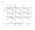
- FIG. 4 is a circuit diagram illustrating a display apparatus using a mechanical switch according to an exemplary embodiment of the present invention.
- FIG. 3 is a circuit diagram illustrating a memory array using a mechanical switch according to an exemplary embodiment of the present invention.
- the memory array using the mechanical switch comprises a plurality of word lines (W/L0, W/L1, and W/L2), a plurality of bit lines (B/L0, B/L1, and B/L2), and a plurality of the mechanical switches.
- the plurality of bit lines (B/L0, B/L1, and B/L2) intersects each other with the plurality of word lines (W/L0, W/L1, and W/L2).
- the plurality of mechanical switches is disposed at an intersection of the plurality of word lines (W/L0, W/L1, and W/L2) and the plurality of bit lines (B/L0, B/L1, and B/L2).
- Each of the mechanical switches comprises a gate electrode 120 connecting with each of the word lines (W/L0, W/L1, and W/L2); a drain electrode 140 spaced apart from the gate electrode 120 and connecting to a capacitor 160; and a source electrode 150.
- the source electrode 150 comprises an anchor part 151 spaced apart from the gate electrode 120 and connecting to each of the bit lines (B/L0, B/L1, and B/L2); a mobile part 152 extending from the anchor part 151 and spaced apart from the gate electrode 120; and a dimple 153 extending from the mobile part 152 and formed in a protrusion shape.
- the dimple 153 of the source electrode 150 contacts with the drain electrode 140 by a difference between a voltage applied to the gate electrode 120 and a voltage applied to the source electrode 150, and the voltage applied to the source electrode 150 is transferred to the drain electrode 140.
- V pi a pull-in voltage
- the dimple 153 of the source electrode 150 contacts with the drain electrode 140 so that the voltage applied to the source electrode 150 can be transferred to the capacitor through the drain electrode 140.
- the dimple 153 of the source electrode 150 is again restored to an original position by an elastic force, and does not contact with the drain electrode 140.
- a cantilever is typical.
- the dimple 153 of the source electrode 150 can not only prevents a stiction in a manufacturing process of the mechanical switch but also reduces the pull-in voltage (V pi ).
- the gate electrode 120, the source electrode 150, and the drain electrode 140 can be formed of conductive material comprising any one of copper, carbon nano tube, and polysilicon.
- the plurality of word lines (W/L0, W/L1, and W/L2) and the plurality of bit lines (B/L0, B/L1, and B/L2) can be formed of conductive material comprising any one of copper, carbon nano tube, and polysilicon.
- the capacitor 160 comprises a first electrode 161, a second electrode 163, and a dielectric layer 162 formed between the first electrode 161 and the second electrode 163.
- the first electrode 161 can be manufactured by a conductive semiconductor substrate, or can be manufactured by forming a conductive electrode on a nonconductive substrate. In case where the first electrode is manufactured by the conductive semiconductor substrate, it can use a silicon substrate.
- the dielectric layer 162 can be formed of silicon oxide or silicon nitride.
- the second electrode 163 can be formed of conductive material comprising any one of copper, carbon nano tube, and polysilicon.
- voltages are applied to the plurality of word lines (W/L0, W/L1, and W/L2) under the conditions of o,1 and o,3.
- ) is greater than a difference between the maximal voltage (V B/L , max ) of the bit line and the minimal voltage (V B/L, min ) of the bit line.
- the maximal voltage (V B/L, max ) of the bit line refers to a voltage for indicating a high state of data stored in the capacitor 160.
- the minimal voltage (V B/L, min) of the bit line refers to a voltage for indicating a low state of the data stored in the capacitor 160.
- the voltage (V W/L,selected > V B/L,max + V pi ) greater than the sum of the maximal voltage (V B/L, max ) of the bit line and the pull-in voltage (V pi ) or the voltage (V W/L,selected ⁇ V B/L,min -V pi ) smaller than the difference between the minimal voltage (V B/L, min ) of the bit line and the pull-in voltage (V pi ) is applied to the word line (W/L0).
- the maximal voltage (V B/L , max ) of the bit line or the minimal voltage (V B/L , min ) of the bit line are applied to the bit line.
- FIG. 4 is a circuit diagram illustrating a display apparatus using a mechanical switch according to an exemplary embodiment of the present invention.
- the display apparatus using the mechanical switch comprises a plurality of scan lines (S/L0, S/L1, and S/L2), a plurality of data lines (D/L0, D/L1, and D/L2), and a plurality of the mechanical switches.
- the plurality of data lines intersects each other with the plurality of scan lines (S/L0, S/L1, and S/L2).
- the plurality of mechanical switches is disposed at an intersection of the plurality of scan lines (S/L0, S/L1, and S/L2) and the plurality of data lines (D/L0, D/L1, and D/L2).
- Each of the mechanical switches comprises a gate electrode 220 connecting with each of the scan lines (S/L0, S/L1, and S/L2); a drain electrode 240 spaced apart from the gate electrode 220 and connecting to a pixel 260; and a source electrode 250.
- the source electrode 250 comprises an anchor part 251 spaced apart from the gate electrode 220 and connecting to each of the data lines (D/L0, D/L1, and D/L2); a mobile part 252 extending from the anchor part 251 and spaced apart from the gate electrode 220; and a dimple 253 extending from the mobile part 252 and formed in a protrusion shape.
- the dimple 253 of the source electrode 250 electrically contacts with the drain electrode 240 by a difference between a voltage applied to the gate electrode 220 and a voltage applied to the source electrode 250, and the voltage applied to the source electrode 250 is transferred to the drain electrode 240.
- V pi a pull-in voltage
- the dimple 253 of the source electrode 250 contacts with the drain electrode 240 so that the voltage applied to the source electrode 250 can be transferred to the pixel 260 through the drain electrode 240.
- the dimple 253 of the source electrode 250 is again restored to an original position by an elastic force, and does not contact with the drain electrode 240.
- a cantilever is typical.
- the dimple 253 of the source electrode 250 can not only prevents a stiction in a manufacturing process of the mechanical switch but also reduces the pull-in voltage (V pi ).
- the gate electrode 220, the source electrode 250, and the drain electrode 240 can be formed of conductive material comprising any one of copper, carbon nano tube, and polysilicon.
- the plurality of scan lines (S/L0, S/L1, and S/L2) and the plurality of data lines (D/L0, D/L1, and D/L2) can be formed of conductive material comprising any one of copper, carbon nano tube, and polysilicon.
- voltages are applied to the plurality of scan lines (S/L0, S/L1, and S/L2) under the conditions of o,1 and o,3, o,1 Condition of applying voltage to selected scan line: V S / L , selected - V D / L
- ) is greater than a difference between the maximal voltage (V D/L , max ) of the data line and the minimal voltage (V D/L , min ) of the data line.
- the maximal voltage (V D/L , max ) of the data line refers to a maximal data voltage transferred to the pixel 260.
- the minimal voltage (V D/L, min ) of the data line refers to a minimal data voltage transferred to the pixel 260.
- the voltage (V S/L, selected > V D/L, max + V pi ) greater than the sum of the maximal voltage (V D/L , max ) of the data line and the pull-in voltage (V pi ) or the voltage (V S/L, selected ⁇ V D/L, min -V pi ) smaller than the difference between the minimal voltage (V D/L,min ) of the data line and the pull-in voltage (V pi ) is applied to the scan line (S/L0).
- a voltage between the minimal voltage (V D/L, min ) of the data line or the maximal voltage (V D/L, max ) of the data line are applied to the data line.
- the minimal voltage (V D/L , min ) of the data line applied to the data line (D/LO) or the maximal voltage (V D/L , max ) of the data line can be transferred to the pixel 260 through the drain electrode 240, thereby displaying pixel data associated with the voltage between the minimal voltage (V D/L, min ) of the data line or the maximal voltage (V D/L, max ) of the data line.
- the memory array according to an exemplary embodiment of the present invention uses the mechanical switch with the dimple, thereby facilitating its construction without the use of the semiconductor transistor.
- the memory array using the mechanical switch according to an exemplary embodiment of the present invention can be provided as a military or satellite nonvolatile mechanical memory array in which an operation voltage is lower than that of a conventional flash memory, thereby reducing a power consumption, in which an operation speed is made fast, in which there is not a degradation of an electrical reliability like a breakdown of a gate insulating film, and in which a sensitivity to an external harmful environment such as radiation is poor.
- the use of the conductive electrode on an arbitrary substrate instead of the semiconductor substrate can provide the memory array in which integration can be implemented irrespective of a substrate kind as well as a multi-bit cell storage can be made, as it easily transfers any source voltage to the drain in the capacitor.
- the application voltage of the selected word line and the application voltage of the unselected word line can be controlled, thereby effectively selecting the memory cell of the memory array.
- the mechanical switch with the dimple can be used, thereby easily constructing the display apparatus without the use of the semiconductor transistor.
- the application voltage of the selected scan line and the application voltage of the unselected scan line can be controlled, thereby effectively displaying a data voltage in the pixel cell.
Landscapes
- Engineering & Computer Science (AREA)
- Chemical & Material Sciences (AREA)
- Nanotechnology (AREA)
- Physics & Mathematics (AREA)
- Mathematical Physics (AREA)
- Theoretical Computer Science (AREA)
- Crystallography & Structural Chemistry (AREA)
- Semiconductor Memories (AREA)
- Devices For Indicating Variable Information By Combining Individual Elements (AREA)
- Control Of Indicators Other Than Cathode Ray Tubes (AREA)
Abstract
Description
- The present invention relates to a memory array using a mechanical switch, a method for controlling the same, a display apparatus using a mechanical switch, and a method for controlling the same, and more particularly, to a memory array constructed using a mechanical switch, a method for controlling the memory array, a display apparatus constructed using a mechanical switch, and a method for controlling the display apparatus.
- Until now, a degree of integration of a semiconductor transistor greatly increases according to Moore's law, thereby much contributing to the development of a semiconductor industry. In general, the semiconductor transistor has been used as a switching device using an on or off characteristic and an amplifying device using a current and voltage amplification characteristic. In a digital integration circuit particularly, the semiconductor transistor has been mainly used as the switching device. However, the semiconductor transistor has a drawback that it should be necessarily formed on a semiconductor substrate and thus, should consider a body effect of the semiconductor substrate. Particularly, the semiconductor transistor has a drawback of a leakage of electrical charges inevitably caused by its internal leakage source. In addition, the semiconductor transistor has a drawback that its sensitivity to an external harmful environment such as radiation causes a soft error (SE). The semiconductor transistor has a drawback that a degradation of its gate oxide causes a reduction of an electrical reliability, and an increase of the degree of integration causes a short channel effect such as junction leakage and hot electron injection.
- In order to overcome conventional several drawbacks of the semiconductor transistor serving as the switching device, a mechanical switch using a recent Micro-ElectroMechanical System (MEMS) or Nano-ElectroMechanical System (NEMS) is being researched and developed.
- FIG. 1 is a conceptual diagram illustrating a conventional mechanical switch. Referring to FIG. 1, the conventional mechanical switch, which is disclosed in
U.S. Patent No. 6,534,839 and W. H. Teh, et. al., "Switching characteristics of electrostatically actuated miniaturized micromechanical metallic catilevers", J. Vac. Sci. Technol., B. 21, pp. 2360-2367, 2003, is of a structure comprising agate electrode 10, adrain electrode 30, and asource electrode 20 comprised of ananchor part 21 and amobile part 22. An operation of the mechanical switch is characterized in that themobile part 22 of thesource electrode 20 electrically contacts with thedrain electrode 30, thereby electrically conducting thesource electrode 20 and thedrain electrode 30 in generation of an electrostatic force based on a voltage difference between thegate electrode 10 and thesource electrode 20, and thesource electrode 20 and thedrain electrode 30 are electrically disconnected in the absence of the generation of the electrostatic force. - Specifically, operation of the mechanical switch by the electrostatic force is based on, not a principle in which the
mobile part 22 of thesource electrode 20 is linearly displaced toward thedrain electrode 30 and is in electric contact with thedrain electrode 30 in proportional to the voltage difference between thesource electrode 20 and thegate electrode 10, but a principle in which an unstable state (Hereinafter, referred to as "pull-in state") where the electrostatic force between themobile part 22 of thesource electrode 20 and thegate electrode 10 is greater than an elastic resilient force of themobile part 22 of thesource electrode 20 at more than a certain voltage (Hereinafter, referred to as "pull-in voltage (Vpi)") between two electrodes occurs, and themobile part 22 of thesource electrode 20 instantaneously gets in electric contact with thedrain electrode 30. In other words, the pull-in voltage can be defined as the voltage difference between thesource electrode 20 and thegate electrode 10, required for electrically conducting thesource electrode 20 and thedrain electrode 30 of the mechanical switch. The pull-in state occurs when themobile part 22 of thesource electrode 20 shifts by one third of a distance between themobile part 22 of thesource electrode 20 and thegate electrode 10. The pull-in voltage is similar in function with a threshold voltage of a metal oxide semiconductor (MOS) transistor (H. C. Nathanson, et. al., "The resonant gate transistor", IEEE Transactions on Electron Devices, Vol. ED-104, No. 3, pp. 117-133, 1967). -
U.S. Patent No. 6,509,605 discloses a memory array constructed using a mechanical switch, in which a operation voltage is low and a operation speed is fast and thus, a power consumption is low and writing and reading time are short as well as an electrical reliability is not deteriorated because of mechanical actuation, and a sensitivity to radiation is poor. The '605 memory array is being researched and developed as a next generation memory array to replace a conventional memory array. However, the memory array cannot be controlled because of its construction using only the mechanical switch and thus, has a drawback in that it should be constructed in combination with a complementary metal oxide semiconductor (CMOS) transistor. Accordingly, the memory array gets so complex in construction and process and causes a scaling limit, thereby reducing a degree of integration. - A research for using the mechanical switch as a selection transistor of a display apparatus (
U.S. Patent No. 4,681,403 ) such as a liquid crystal display (LCD), thereby being more advantageous for a large-area integration, and more improving a product yield and a manufacturing cost owing to a simple manufacturing process than in conventional MOS transistor or thin film transistor (TFT) is in progress. However, the display apparatus using the mechanical switch disclosed in the U.S. Patent '403 has a disadvantage in that a pixel voltage for embodying a gray level cannot variously be changeable. - FIG. 2 is a circuit diagram illustrating a conventional memory array using a MOS transistor. Referring to FIG. 2, an input voltage of a source voltage or a ground voltage is applied to a bit line (B/LO) connecting to a selected MOS transistor of a
memory cell 90, and a threshold voltage or more of the MOS transistor is applied to a word line (W/L0) connecting to the selected MOS transistor. Thus, the applied voltage of the bit line (B/LO) is transferred to astorage unit 80 through electrically conductedsource electrode 60 anddrain electrode 70, and the applied voltage of the bit line (B/L0) is stored in thestorage unit 80. Less than the threshold voltage is applied to word lines (W/L1 and W/L2) not connecting to the selected MOS transistor. Thus, thesource electrode 60 and thedrain electrode 70 electrically disconnect with each other, and the applied voltage of the bit line is not transferred to thestorage unit 80. A method for controlling the memory array using the MOS transistor is different from a method for controlling a memory array using a mechanical switch. Therefore, a control method different from the conventional method of controlling the memory array using the MOS transistor is being required for effectively controlling the memory array using the mechanical switch. - Accordingly, the present invention is to provide a memory array constructed using a mechanical switch with a dimple.
- Also, the present invention is to provide a method for controlling a memory array using a mechanical switch.
- Also, the present invention is to provide a display apparatus constructed using a mechanical switch with a dimple.
- Also, the present invention is to provide a method for controlling a display apparatus using a mechanical switch.
- In one aspect, there is provided a memory array using a mechanical switch. The memory array comprises a plurality of word lines, a plurality of bit lines intersecting each other with the plurality of word lines, and a plurality of the mechanical switches. The mechanical switch disposed at an intersection of the plurality of word lines and the plurality of bit lines comprises a gate electrode connecting with each of the word lines, a drain electrode spaced apart from the gate electrode and connecting to a capacitor, and a source electrode. The source electrode comprises an anchor part spaced apart from the gate electrode and connecting to each of the bit lines, a mobile part extending from the anchor part and spaced apart from the gate electrode, and a dimple extending from the mobile part and formed in a protrusion shape.
- Implementations may include one or more of the following features. For example, in each of the mechanical switches, the dimple of the source electrode electrically contacts with the drain electrode by a difference between a voltage applied to the gate electrode and a voltage applied to the source electrode, and the voltage applied to the source electrode is transferred to the drain electrode.
- Implementations may include one or more of the following features. For example, the capacitor comprises a first electrode, a second electrode, and a dielectric layer formed between the first electrode and the second electrode.
- Implementations may include one or more of the following features. For example, the first electrode is a conductive electrode formed on a conductive semiconductor substrate or a nonconductive semiconductor substrate.
- Implementations may include one or more of the following features. For example, the dielectric layer is formed of silicon oxide or silicon nitride.
- Implementations may include one or more of the following features. For example, the second electrode is formed of conductive material comprising any one of copper, carbon nano tube, and polysilicon.
- Implementations may include one or more of the following features. For example, the gate electrode, the source electrode, and the drain electrode of each of the mechanical switches are formed of conductive material comprising any one of copper, carbon nano tube, and polysilicon.
- Implementations may include one or more of the following features. For example, the plurality of word lines and the plurality of bit lines are formed of conductive material comprising any one of copper, carbon nano tube, and polysilicon.
- In another aspect, there is provided a method for controlling a memory array using a mechanical switch, in which the memory array comprises a plurality of word lines, a plurality of bit lines intersecting each other with the plurality of word lines, and a plurality of the mechanical switches. The mechanical switch disposed at an intersection of the plurality of word lines and the plurality of bit lines comprises a gate electrode connecting with each of the word lines, a drain electrode spaced apart from the gate electrode and connecting to a capacitor, and a source electrode. The source electrode comprises an anchor part spaced apart from the gate electrode and connecting to each of the bit lines, a mobile part extending from the anchor part and spaced apart from the gate electrode, and a dimple extending from the mobile part and formed in a protrusion shape. The method comprises steps of: applying a voltage greater than a sum of a maximal voltage (VB/L, max) of the bit line and a pull-in voltage or a voltage smaller than a difference between a minimal voltage (VB/L, min) of the bit line and the pull-in voltage, to the word line selected from the plurality of word lines; and applying a voltage smaller than a sum of the minimal voltage (VB/L, min) of the bit line and the pull-in voltage and greater than a difference between the maximal voltage (VB/L, max) of the bit line and the pull-in voltage, to the word lines unselected from the plurality of word lines.
- Implementations may include one or more of the following features. For example, the pull-in voltage is greater than a difference between the maximal voltage (VB/L, max) of the bit line and the minimal voltage (VB/L, min) of the bit line.
- In a further another aspect, there is provided a display apparatus using a mechanical switch. The display apparatus comprises a plurality of scan lines, a plurality of data lines intersecting each other with the plurality of scan lines, and a plurality of the mechanical switches. The mechanical switch disposed at an intersection of the plurality of word lines and the plurality of bit lines comprises a gate electrode connecting with each of the word lines, a drain electrode spaced apart from the gate electrode and connecting to a capacitor, and a source electrode. The source electrode comprises an anchor part spaced apart from the gate electrode and connecting to each of the bit lines, a mobile part extending from the anchor part and spaced apart from the gate electrode, and a dimple extending from the mobile part and formed in a protrusion shape.
- Implementations may include one or more of the following features. For example, in each of the mechanical switches, the dimple of the source electrode electrically contacts with the drain electrode by a difference between a voltage applied to the gate electrode and a voltage applied to the source electrode, and the voltage applied to the source electrode is transferred to the drain electrode.
- Implementations may include one or more of the following features. For example, the gate electrode, the source electrode, and the drain electrode of each of the mechanical switches are formed of conductive material comprising any one of copper, carbon nano tube, and polysilicon.
- Implementations may include one or more of the following features. For example, the plurality of scan lines and the plurality of data lines are formed of conductive material comprising any one of copper, carbon nano tube, and polysilicon.
- In a still further another aspect, there is provided a method for controlling a display apparatus using a mechanical switch, in which the display apparatus comprises a plurality of scan lines, a plurality of data lines intersecting each other with the plurality of scan lines, and a plurality of the mechanical switches. The mechanical switch disposed at an intersection of the plurality of word lines and the plurality of bit lines comprises a gate electrode connecting with each of the word lines, a drain electrode spaced apart from the gate electrode and connecting to a capacitor, and a source electrode. The source electrode comprises an anchor part spaced apart from the gate electrode and connecting to each of the bit lines, a mobile part extending from the anchor part and spaced apart from the gate electrode, and a dimple extending from the mobile part and formed in a protrusion shape. The method comprises steps of: applying a voltage greater than a sum of a maximal voltage (VD/L, max) of the data line and a pull-in voltage or a voltage smaller than a difference between a minimal voltage (VD/L, min) of the data line and the pull-in voltage, to the scan line selected from the plurality of scan lines, and applying a voltage smaller than a sum of the minimal voltage (VD/L, min) of the data line and the pull-in voltage and greater than a difference between the maximal voltage (VD/L, max) of the data line and the pull-in voltage, to the scan lines unselected from the plurality of scan lines.
- Implementations may include one or more of the following features. For example, the pull-in voltage is greater than a difference between the maximal voltage (VD/L, max) of the data line and the minimal voltage (VD/L, min) of the data line.
- It is to be understood that both the foregoing general description and the following detailed description are exemplary and explanatory and are intended to provide further explanation of the invention as claimed.
- The invention will be described in detail with reference to the following drawings in which like numerals refer to like elements.
- FIG. 1 is a conceptual diagram illustrating a conventional mechanical switch;
- FIG. 2 is a circuit diagram illustrating a conventional memory array using a MOS transistor;
- FIG. 3 is a circuit diagram illustrating a memory array using a mechanical switch according to an exemplary embodiment of the present invention; and
- FIG. 4 is a circuit diagram illustrating a display apparatus using a mechanical switch according to an exemplary embodiment of the present invention.
- Preferred embodiments of the present invention will be described in a more detailed manner with reference to the drawings.
- FIG. 3 is a circuit diagram illustrating a memory array using a mechanical switch according to an exemplary embodiment of the present invention.
- As shown in FIG. 3, the memory array using the mechanical switch according to an exemplary embodiment of the present invention comprises a plurality of word lines (W/L0, W/L1, and W/L2), a plurality of bit lines (B/L0, B/L1, and B/L2), and a plurality of the mechanical switches.
- The plurality of bit lines (B/L0, B/L1, and B/L2) intersects each other with the plurality of word lines (W/L0, W/L1, and W/L2). The plurality of mechanical switches is disposed at an intersection of the plurality of word lines (W/L0, W/L1, and W/L2) and the plurality of bit lines (B/L0, B/L1, and B/L2). Each of the mechanical switches comprises a
gate electrode 120 connecting with each of the word lines (W/L0, W/L1, and W/L2); adrain electrode 140 spaced apart from thegate electrode 120 and connecting to acapacitor 160; and asource electrode 150. Thesource electrode 150 comprises ananchor part 151 spaced apart from thegate electrode 120 and connecting to each of the bit lines (B/L0, B/L1, and B/L2); amobile part 152 extending from theanchor part 151 and spaced apart from thegate electrode 120; and adimple 153 extending from themobile part 152 and formed in a protrusion shape. - In each of the plurality of mechanical switches, the
dimple 153 of thesource electrode 150 contacts with thedrain electrode 140 by a difference between a voltage applied to thegate electrode 120 and a voltage applied to thesource electrode 150, and the voltage applied to thesource electrode 150 is transferred to thedrain electrode 140. In other words, when the difference between the voltage applied to thegate electrode 120 and the voltage applied to thesource electrode 150 is more than a pull-in voltage (Vpi), an electrostatic force is generated, thereby making thedimple 153 of thesource electrode 150 electrically contact with thedrain electrode 140, and transferring the voltage applied to thesource electrode 150 to thedrain electrode 140. - In generation of the electrostatic force, the
dimple 153 of thesource electrode 150 contacts with thedrain electrode 140 so that the voltage applied to thesource electrode 150 can be transferred to the capacitor through thedrain electrode 140. In the absence of the generation of the electrostatic force, thedimple 153 of thesource electrode 150 is again restored to an original position by an elastic force, and does not contact with thedrain electrode 140. As such a structure, a cantilever is typical. Also, thedimple 153 of thesource electrode 150 can not only prevents a stiction in a manufacturing process of the mechanical switch but also reduces the pull-in voltage (Vpi). - In each of the plurality of mechanical switches, the
gate electrode 120, thesource electrode 150, and thedrain electrode 140 can be formed of conductive material comprising any one of copper, carbon nano tube, and polysilicon. The plurality of word lines (W/L0, W/L1, and W/L2) and the plurality of bit lines (B/L0, B/L1, and B/L2) can be formed of conductive material comprising any one of copper, carbon nano tube, and polysilicon. - The
capacitor 160 comprises afirst electrode 161, asecond electrode 163, and adielectric layer 162 formed between thefirst electrode 161 and thesecond electrode 163. Thefirst electrode 161 can be manufactured by a conductive semiconductor substrate, or can be manufactured by forming a conductive electrode on a nonconductive substrate. In case where the first electrode is manufactured by the conductive semiconductor substrate, it can use a silicon substrate. Thedielectric layer 162 can be formed of silicon oxide or silicon nitride. Thesecond electrode 163 can be formed of conductive material comprising any one of copper, carbon nano tube, and polysilicon. - In order to effectively control memory cells of the memory array using the mechanical switch according to an exemplary embodiment of the present invention, voltages are applied to the plurality of word lines (W/L0, W/L1, and W/L2) under the conditions of o,1 and o,3.
o,1 Condition of applying voltage to selected word line:
o,2 Condition of applying voltage to unselected word line:
o,3 Pull-in voltage:
- A voltage (VW/L,selected > VB/L,max+ Vpi) greater than a sum of a maximal voltage (VB/L, max) of the bit line and the pull-in voltage (Vpi) or a voltage (VW/L,selected < VB/L,min-Vpi) smaller than a difference between a minimal voltage (VB/L, min) of the bit line and the pull-in voltage (Vpi) is applied to the word line (W/L0) selected from the plurality of word lines (W/L0, W/L1, and W/L2). A voltage (VB/L, max - Vpi < VW/L,unselected < VB/L,min + Vpi) smaller than a sum of the minimal voltage (VB/L, min) of the bit line and the pull-in voltage (Vpi) and greater than a difference between the maximal voltage (VB/L, max) of the bit line and the pull-in voltage (Vpi) is applied to the word lines (W/L1 and W/L2) unselected from the plurality of word lines (W/L0, W/L1, and W/L2). The pull-in voltage (Vpi>|VB/L,max-VB/L,min|) is greater than a difference between the maximal voltage (VB/L, max) of the bit line and the minimal voltage (VB/L, min) of the bit line. The maximal voltage (VB/L, max) of the bit line refers to a voltage for indicating a high state of data stored in the
capacitor 160. The minimal voltage (VB/L,min) of the bit line refers to a voltage for indicating a low state of the data stored in thecapacitor 160. - For example, in case where the
memory cell 170 is selected, the voltage (VW/L,selected > VB/L,max + Vpi) greater than the sum of the maximal voltage (VB/L, max) of the bit line and the pull-in voltage (Vpi) or the voltage (VW/L,selected <VB/L,min-Vpi) smaller than the difference between the minimal voltage (VB/L, min) of the bit line and the pull-in voltage (Vpi) is applied to the word line (W/L0). The voltage (VB/L,max - Vpi < VW/L,unselected < VB/L,min + Vpi) smaller than the sum of the minimal voltage (VB/L, min) of the bit line and the pull-in voltage (Vpi) and greater than the difference between the maximal voltage (VB/L, max) of the bit line and the pull-in voltage (Vpi) is applied to the word lines (W/L1 and W/L2). The maximal voltage (VB/L, max) of the bit line or the minimal voltage (VB/L, min) of the bit line are applied to the bit line. - Under the conditions, a difference between the application voltage of the
gate electrode 120 connecting to the word line (W/L0) and the application voltage of thesource electrode 150 connecting to the bit line (B/L0) becomes more than the pull-in voltage. Therefore, the electrostatic force is generated and thedimple 153 of thesource electrode 150 contacts with thedrain electrode 140. By doing so, the maximal voltage (VB/L, max) of the bit line applied to the bit line (B/LO) or the minimal voltage (VB/L, min) of the bit line can be transferred to thecapacitor 160 through thedrain electrode 140, and can be stored in thecapacitor 160. - FIG. 4 is a circuit diagram illustrating a display apparatus using a mechanical switch according to an exemplary embodiment of the present invention.
- As shown in FIG. 4, the display apparatus using the mechanical switch according to an exemplary embodiment of the present invention comprises a plurality of scan lines (S/L0, S/L1, and S/L2), a plurality of data lines (D/L0, D/L1, and D/L2), and a plurality of the mechanical switches.
- The plurality of data lines (D/L0, D/L1, and D/L2) intersects each other with the plurality of scan lines (S/L0, S/L1, and S/L2). The plurality of mechanical switches is disposed at an intersection of the plurality of scan lines (S/L0, S/L1, and S/L2) and the plurality of data lines (D/L0, D/L1, and D/L2). Each of the mechanical switches comprises a
gate electrode 220 connecting with each of the scan lines (S/L0, S/L1, and S/L2); adrain electrode 240 spaced apart from thegate electrode 220 and connecting to apixel 260; and asource electrode 250. Thesource electrode 250 comprises ananchor part 251 spaced apart from thegate electrode 220 and connecting to each of the data lines (D/L0, D/L1, and D/L2); amobile part 252 extending from theanchor part 251 and spaced apart from thegate electrode 220; and adimple 253 extending from themobile part 252 and formed in a protrusion shape. - In each the plurality of mechanical switches, the
dimple 253 of thesource electrode 250 electrically contacts with thedrain electrode 240 by a difference between a voltage applied to thegate electrode 220 and a voltage applied to thesource electrode 250, and the voltage applied to thesource electrode 250 is transferred to thedrain electrode 240. In other words, when the difference between the voltage applied to thegate electrode 220 and the voltage applied to thesource electrode 250 is more than a pull-in voltage (Vpi), an electrostatic force is generated, thereby making thedimple 253 of thesource electrode 250 electrically contact with thedrain electrode 240, and transferring the voltage applied to thesource electrode 250 to thedrain electrode 240. - In generation of the electrostatic force, the
dimple 253 of thesource electrode 250 contacts with thedrain electrode 240 so that the voltage applied to thesource electrode 250 can be transferred to thepixel 260 through thedrain electrode 240. In the absence of the generation of the electrostatic force, thedimple 253 of thesource electrode 250 is again restored to an original position by an elastic force, and does not contact with thedrain electrode 240. As such a structure, a cantilever is typical. Also, thedimple 253 of thesource electrode 250 can not only prevents a stiction in a manufacturing process of the mechanical switch but also reduces the pull-in voltage (Vpi). - In each of the plurality of mechanical switches, the
gate electrode 220, thesource electrode 250, and thedrain electrode 240 can be formed of conductive material comprising any one of copper, carbon nano tube, and polysilicon. The plurality of scan lines (S/L0, S/L1, and S/L2) and the plurality of data lines (D/L0, D/L1, and D/L2) can be formed of conductive material comprising any one of copper, carbon nano tube, and polysilicon. - In order to effectively control pixel cells of the display apparatus using the mechanical switch according to an exemplary embodiment of the present invention, voltages are applied to the plurality of scan lines (S/L0, S/L1, and S/L2) under the conditions of o,1 and o,3,
o,1 Condition of applying voltage to selected scan line:

o,2 Condition of applying voltage to unselected scan line:

o,3 Pull-in voltage:
- A voltage (VS,L,selected > VD,L,max +Vpi) greater than a sum of a maximal voltage (VD/L, max) of the data line and the pull-in voltage (Vpi) or a voltage (VS/L,selected < VD/L,min - Vpi) smaller than a difference between a minimal voltage (VD/L, min) of the data line and the pull-in voltage (Vpi) is applied to the scan line (S/L0) selected from the plurality of scan lines (S/L0, S/L1, and S/L2). A voltage (VD/L, max-Vpi < VS/L, unselected < VD/L,min + Vpi) smaller than a sum of the minimal voltage (VD/L, min) of the data line and the pull-in voltage (Vpi) and greater than a difference between the maximal voltage (VD/L, max) of the data line and the pull-in voltage (Vpi) is applied to the scan lines (S/L1 and S/L2) unselected from the plurality of scan lines (S/L0, S/L1, and S/L2). The pull-in voltage (Vpi > |VD/max - VD/L,min|) is greater than a difference between the maximal voltage (VD/L, max) of the data line and the minimal voltage (VD/L, min) of the data line. The maximal voltage (VD/L, max) of the data line refers to a maximal data voltage transferred to the
pixel 260. The minimal voltage (VD/L, min) of the data line refers to a minimal data voltage transferred to thepixel 260. - For example, in case where the
pixel cell 270 is selected, the voltage (VS/L, selected > VD/L, max + Vpi) greater than the sum of the maximal voltage (VD/L, max) of the data line and the pull-in voltage (Vpi) or the voltage (VS/L, selected < VD/L, min-Vpi) smaller than the difference between the minimal voltage (VD/L,min) of the data line and the pull-in voltage (Vpi) is applied to the scan line (S/L0). The voltage (VD/L, max-Vpi <VS/L, unselected < VD/L, min + Vpi) smaller than the sum of the minimal voltage (VD/L, min) of the data line and the pull-in voltage (Vpi) and greater than the difference between the maximal voltage (VD/L, max) of the data line and the pull-in voltage (Vpi) is applied to the scan lines (S/L1 and S/L2). A voltage between the minimal voltage (VD/L, min) of the data line or the maximal voltage (VD/L, max) of the data line are applied to the data line. - Under the conditions, a difference between the application voltage of the
gate electrode 220 connecting to the scan line (S/L0) and the application voltage of thesource electrode 250 connecting to the data line (D/L0) becomes more than the pull-in voltage (Vpi). Therefore, the electrostatic force is generated and thedimple 253 of thesource electrode 250 electrically contacts with thedrain electrode 240. By doing so, the minimal voltage (VD/L, min) of the data line applied to the data line (D/LO) or the maximal voltage (VD/L, max) of the data line can be transferred to thepixel 260 through thedrain electrode 240, thereby displaying pixel data associated with the voltage between the minimal voltage (VD/L, min) of the data line or the maximal voltage (VD/L, max) of the data line. - As described above, the memory array according to an exemplary embodiment of the present invention uses the mechanical switch with the dimple, thereby facilitating its construction without the use of the semiconductor transistor.
- Also, the memory array using the mechanical switch according to an exemplary embodiment of the present invention can be provided as a military or satellite nonvolatile mechanical memory array in which an operation voltage is lower than that of a conventional flash memory, thereby reducing a power consumption, in which an operation speed is made fast, in which there is not a degradation of an electrical reliability like a breakdown of a gate insulating film, and in which a sensitivity to an external harmful environment such as radiation is poor.
- The use of the conductive electrode on an arbitrary substrate instead of the semiconductor substrate can provide the memory array in which integration can be implemented irrespective of a substrate kind as well as a multi-bit cell storage can be made, as it easily transfers any source voltage to the drain in the capacitor.
- In the method for controlling the memory array using the mechanical switch according to an exemplary embodiment of the present invention, the application voltage of the selected word line and the application voltage of the unselected word line can be controlled, thereby effectively selecting the memory cell of the memory array.
- In the display apparatus using the mechanical switch according to an exemplary embodiment of the present invention, the mechanical switch with the dimple can be used, thereby easily constructing the display apparatus without the use of the semiconductor transistor.
- In the method for controlling the display apparatus using the mechanical switch according to an exemplary embodiment of the present invention, the application voltage of the selected scan line and the application voltage of the unselected scan line can be controlled, thereby effectively displaying a data voltage in the pixel cell.
- The invention being thus described, it will be obvious that the same may be varied in many ways. Such variations are not to be regarded as a departure from the spirit and scope of the invention, and all such modifications as would be obvious to one skilled in the art are intended to be included within the scope of the following claims.
Claims (16)
- A memory array using a mechanical switch, the memory array comprising:a plurality of word lines (W/L0, W/L1, W/L2);a plurality of bit lines (B/L0, B/L1, BL2) intersecting each other with the plurality of word lines (W/L0, W/L1, W/L2); anda plurality of the mechanical switches,the mechanical switch disposed at an intersection of the plurality ofword lines (W/L0, W/L1, W/L2) and the plurality of bit lines (B/L0,B/L1, B/L2), and comprising:a gate electrode (120) connecting with each of the word lines;a drain electrode (140) spaced apart from the gate electrode (120) and connecting to a capacitor (160); anda source electrode (150),the source electrode (150) comprising:an anchor part (151) spaced apart from the gate electrode (120) and connecting to each of the bit lines;a mobile part (152) extending from the anchor part (151) and spaced apart from the gate electrode (120); anda dimple (153) extending from the mobile part (152) and formed in a protrusion shape.
- The memory array of claim 1, wherein, in each of the mechanical switches, the dimple (153) of the source electrode (150) electrically contacts with the drain electrode (140) by a difference between a voltage applied to the gate electrode (120) and a voltage applied to the source electrode (150), and the voltage applied to the source electrode (150) is transferred to the drain electrode (140).
- The memory array of claim 1, wherein the capacitor (160) comprises a first electrode (161), a second electrode (163), and a dielectric layer (162) formed between the first electrode (161) and the second electrode (163).
- The memory array of claim 3, wherein the first electrode (161) is a conductive electrode formed on a conductive semiconductor substrate or a nonconductive semiconductor substrate.
- The memory array of claim 3, wherein the dielectric layer (162) is formed of silicon oxide or silicon nitride.
- The memory array of claim 3, wherein the second electrode (163) is formed of conductive material comprising any one of copper, carbon nano tube, and polysilicon.
- The memory array of claim 1, wherein the gate electrode (120), the source electrode (150), and the drain electrode (140) of each of the mechanical switches is formed of conductive material comprising any one of copper, carbon nano tube, and polysilicon.
- The memory array of claim 1, wherein the plurality of word lines (W/L0, W/L1, W/L2) and the plurality of bit lines (B/L0, B/L1, B/L2) are formed of conductive material comprising any one of copper, carbon nano tube, and polysilicon.
- A method for controlling a memory array using a mechanical switch, in which the memory array comprises: a plurality of word lines (W/L0, W/L1, W/L2); a plurality of bit lines (B/L0, B/L1, B/L2) intersecting each other with the plurality of word lines (W/L0, W/L1, W/L2); and a plurality of the mechanical switches, and the mechanical switch disposed at an intersection of the plurality of word lines (W/L0, W/L1, W/L2) and the plurality of bit lines (B/L0, B/L1, B/L2) comprises: a gate electrode (120) connecting with each of the word lines; a drain electrode (140) spaced apart from the gate electrode (120) and connecting to a capacitor (160); and a source electrode (150), and the source electrode (150) comprises: an anchor part (151) spaced apart from the gate electrode (120) and connecting to each of the bit lines; a mobile part (152) extending from the anchor part (151) and spaced apart from the gate electrode (120); and a dimple (153) extending from the mobile part (152) and formed in a protrusion shape, the method comprising steps of:applying a voltage greater than a sum of a maximal voltage (VB/L, max) of the bit line and a pull-in voltage or a voltage smaller than a difference between a minimal voltage (VB/L, min) of the bit line and the pull-in voltage, to the word line selected from the plurality of word lines; andapplying a voltage smaller than a sum of the minimal voltage (VB/L, min) of the bit line and the pull-in voltage and greater than a difference between the maximal voltage (VB/L, max) of the bit line and the pull-in voltage, to the word lines unselected from the plurality of word lines.
- The method of claim 9, wherein the pull-in voltage is greater than a difference between the maximal voltage (VB/L, max) of the bit line and the minimal voltage (VB/L, min) of the bit line.
- A display apparatus using a mechanical switch, the display apparatus comprising:a plurality of scan lines (S/L0, S/L1, S/L2);a plurality of data lines (D/L0, D/L1, D/L2) intersecting each other with the plurality of scan lines (S/L0, S/L1, S/L2); anda plurality of the mechanical switches,the mechanical switch disposed at an intersection of the plurality of scan lines (S/L0, S/L1, S/L2) and the plurality of data lines (D/L0, D/L1, D/L2), and comprising:a gate electrode (220) connecting with each of the scan lines;a drain electrode (240) spaced apart from the gate electrode (220) and connecting to a pixel (260); anda source electrode (250),the source electrode (250) comprising:an anchor part (251) spaced apart from the gate electrode (220) and connecting to each of the data lines;a mobile part (252) extending from the anchor part (251) and spaced apart from the gate electrode (220); anda dimple (253) extending from the mobile part (252) and formed in a protrusion shape.
- The display apparatus of claim 11, wherein in each of the mechanical switches, the dimple (253) of the source electrode (250) electrically contacts with the drain electrode (240) by a difference between a voltage applied to the gate electrode (220) and a voltage applied to the source electrode (250), and the voltage applied to the source electrode (250) is transferred to the drain electrode (240).
- The display apparatus of claim 11, wherein the gate electrode (220), the source electrode (250), and the drain electrode (240) of each of the mechanical switches is formed of conductive material comprising any one of copper, carbon nano tube, and polysilicon.
- The display apparatus of claim 11, wherein the plurality of scan lines (S/L0, S/L1, S/L2) and the plurality of data lines (D/L0, D/L1, D/L2) are formed of conductive material comprising any one of copper, carbon nano tube, and polysilicon.
- A method for controlling a display apparatus using a mechanical switch, in which the display apparatus comprises: a plurality of scan lines (S/L0, S/L1, S/L2); a plurality of data lines (D/L0, D/L1, D/L2) intersecting each other with the plurality of scan lines (S/L0, S/L1, S/L2); and a plurality of the mechanical switches, and the mechanical switch disposed at an intersection of the plurality of scan lines (S/L0, S/L1, S/L2) and the plurality of data lines (D/L0, D/L1, D/L2) comprises: a gate electrode (220) connecting with each of the scan lines; a drain electrode (240) spaced apart from the gate electrode (220) and connecting to a pixel (260); and a source electrode (250), and the source electrode (250) comprises: an anchor part (251) spaced apart from the gate electrode (220) and connecting to each of the data lines; a mobile part (252) extending from the anchor part (251) and spaced apart from the gate electrode (220); and a dimple (253) extending from the mobile part (252) and formed in a protrusion shape, the method comprising steps of:applying a voltage greater than a sum of a maximal voltage (VD/L, max) of the data line and a pull-in voltage or a voltage smaller than a difference between a minimal voltage (VD/L, min) of the data line and the pull-in voltage, to the scan line selected from the plurality of scan lines; andapplying a voltage smaller than a sum of the minimal voltage (VD/L, min) of the data line and the pull-in voltage and greater than a difference between the maximal voltage (VD/L, max) of the data line and the pull-in voltage, to the scan lines unselected from the plurality of scan lines.
- The method of claim 15, wherein the pull-in voltage is greater than a difference between the maximal voltage (VD/L, max) of the data line and the minimal voltage (VD/L, min) of the data line.
Applications Claiming Priority (1)
| Application Number | Priority Date | Filing Date | Title |
|---|---|---|---|
| KR1020050114665A KR100651825B1 (en) | 2005-11-29 | 2005-11-29 | Memory array using mechanical switch, control method thereof, display device using mechanical switch and control method thereof |
Publications (3)
| Publication Number | Publication Date |
|---|---|
| EP1793386A2 true EP1793386A2 (en) | 2007-06-06 |
| EP1793386A3 EP1793386A3 (en) | 2007-09-19 |
| EP1793386B1 EP1793386B1 (en) | 2012-04-04 |
Family
ID=37731505
Family Applications (1)
| Application Number | Title | Priority Date | Filing Date |
|---|---|---|---|
| EP06123877A Not-in-force EP1793386B1 (en) | 2005-11-29 | 2006-11-10 | A memory array and a display apparatus using mechanical switch, method for controlling the same |
Country Status (6)
| Country | Link |
|---|---|
| US (1) | US7486539B2 (en) |
| EP (1) | EP1793386B1 (en) |
| JP (1) | JP2007149318A (en) |
| KR (1) | KR100651825B1 (en) |
| CN (1) | CN100552820C (en) |
| AT (1) | ATE552593T1 (en) |
Families Citing this family (14)
| Publication number | Priority date | Publication date | Assignee | Title |
|---|---|---|---|---|
| KR100857085B1 (en) | 2007-05-18 | 2008-09-05 | 한국과학기술원 | Operation Method of Memory Array Using Mechanical Switch |
| US8223285B2 (en) | 2007-11-09 | 2012-07-17 | Seiko Epson Corporation | Active matrix device, method for manufacturing switching element, electro-optical display device, and electronic apparatus |
| JP4561813B2 (en) * | 2007-11-09 | 2010-10-13 | セイコーエプソン株式会社 | Active matrix device, electro-optical display device, and electronic apparatus |
| JP4518200B2 (en) * | 2007-11-09 | 2010-08-04 | セイコーエプソン株式会社 | Active matrix device, switching element manufacturing method, electro-optical display device, and electronic apparatus |
| KR100896981B1 (en) * | 2007-12-18 | 2009-05-14 | 한국과학기술원 | Driving Method of Memory Array |
| JP5381216B2 (en) * | 2009-03-25 | 2014-01-08 | セイコーエプソン株式会社 | Electro-optical device and electronic apparatus |
| JP5381217B2 (en) * | 2009-03-25 | 2014-01-08 | セイコーエプソン株式会社 | Electro-optical device and electronic apparatus |
| CN101995689A (en) * | 2009-08-11 | 2011-03-30 | 江苏丽恒电子有限公司 | Switch array and display array of display device |
| JP5444948B2 (en) * | 2009-08-26 | 2014-03-19 | セイコーエプソン株式会社 | Electro-optic device |
| US8436700B2 (en) * | 2009-09-18 | 2013-05-07 | Easic Corporation | MEMS-based switching |
| US8605499B2 (en) | 2011-04-22 | 2013-12-10 | International Business Machines Corporation | Resonance nanoelectromechanical systems |
| EP2557569A1 (en) | 2011-08-10 | 2013-02-13 | Thomson Licensing | Field programmable read-only memory device |
| US9166054B2 (en) * | 2012-04-13 | 2015-10-20 | Semiconductor Energy Laboratory Co., Ltd. | Semiconductor device and manufacturing method thereof |
| CN106865484A (en) * | 2017-02-06 | 2017-06-20 | 京东方科技集团股份有限公司 | Array base palte and preparation method thereof, display device |
Citations (2)
| Publication number | Priority date | Publication date | Assignee | Title |
|---|---|---|---|---|
| US4681403A (en) | 1981-07-16 | 1987-07-21 | U.S. Philips Corporation | Display device with micromechanical leaf spring switches |
| US6509605B1 (en) | 1999-03-18 | 2003-01-21 | Cavendish Kinetics Limited | Flash memory cell having a flexible element |
Family Cites Families (5)
| Publication number | Priority date | Publication date | Assignee | Title |
|---|---|---|---|---|
| WO2001003190A1 (en) * | 1999-06-30 | 2001-01-11 | Hitachi, Ltd. | Semiconductor integrated circuit device |
| EP1153405B1 (en) * | 1999-12-10 | 2006-09-13 | Koninklijke Philips Electronics N.V. | Electronic devices including micromechanical switches |
| US6534839B1 (en) * | 1999-12-23 | 2003-03-18 | Texas Instruments Incorporated | Nanomechanical switches and circuits |
| CN1317728C (en) * | 2004-01-16 | 2007-05-23 | 清华大学 | Micro mechanical switch with strut beam made of sacrificial layer material |
| US6884950B1 (en) * | 2004-09-15 | 2005-04-26 | Agilent Technologies, Inc. | MEMs switching system |
-
2005
- 2005-11-29 KR KR1020050114665A patent/KR100651825B1/en not_active Expired - Fee Related
-
2006
- 2006-10-27 JP JP2006293083A patent/JP2007149318A/en active Pending
- 2006-11-03 US US11/556,451 patent/US7486539B2/en not_active Expired - Fee Related
- 2006-11-10 CN CNB2006101386599A patent/CN100552820C/en not_active Expired - Fee Related
- 2006-11-10 AT AT06123877T patent/ATE552593T1/en active
- 2006-11-10 EP EP06123877A patent/EP1793386B1/en not_active Not-in-force
Patent Citations (2)
| Publication number | Priority date | Publication date | Assignee | Title |
|---|---|---|---|---|
| US4681403A (en) | 1981-07-16 | 1987-07-21 | U.S. Philips Corporation | Display device with micromechanical leaf spring switches |
| US6509605B1 (en) | 1999-03-18 | 2003-01-21 | Cavendish Kinetics Limited | Flash memory cell having a flexible element |
Non-Patent Citations (2)
| Title |
|---|
| H. C. NATHANSON: "The resonant gate transistor", IEEE TRANSACTIONS ON ELECTRON DEVICES, vol. ED-104, no. 3, 1967, pages 117 - 133 |
| PETERSEN KE: "Micromechanical membrane switches on silicon", INTERNATIONAL BUSINESS MACHINES CORPORATION, vol. 23, no. 4, 1 July 1979 (1979-07-01), pages 376 - 385 |
Also Published As
| Publication number | Publication date |
|---|---|
| EP1793386B1 (en) | 2012-04-04 |
| KR100651825B1 (en) | 2006-12-01 |
| EP1793386A3 (en) | 2007-09-19 |
| JP2007149318A (en) | 2007-06-14 |
| CN100552820C (en) | 2009-10-21 |
| CN1975929A (en) | 2007-06-06 |
| US20070121362A1 (en) | 2007-05-31 |
| US7486539B2 (en) | 2009-02-03 |
| ATE552593T1 (en) | 2012-04-15 |
Similar Documents
| Publication | Publication Date | Title |
|---|---|---|
| EP1793386B1 (en) | A memory array and a display apparatus using mechanical switch, method for controlling the same | |
| US8044442B2 (en) | Metal-insulator-metal (MIM) switching devices | |
| US8576475B2 (en) | MEMS switch | |
| US6054745A (en) | Nonvolatile memory cell using microelectromechanical device | |
| JP4425547B2 (en) | Pulse output circuit, shift register, and electronic device | |
| US20080277718A1 (en) | 1T MEMS scalable memory cell | |
| CN104078465B (en) | Nonvolatile memery unit and the method read | |
| US7349236B2 (en) | Electromechanical memory cell with torsional movement | |
| US8995165B2 (en) | Resistive memory cell | |
| US10026648B2 (en) | FDSOI with on-chip physically unclonable function | |
| CN101132005A (en) | Multi-bit electromechanical memory device and manufacturing method thereof | |
| KR20070060003A (en) | Switch using microelectromechanical system | |
| WO2006137455A1 (en) | Electro-mechanical memory, electric circuit using the same, and electro-mechanical memory drive method | |
| CN115083845A (en) | Micro-electro-mechanical system and micro-electro-mechanical system switch | |
| KR20030017396A (en) | Thin film transistor memory device | |
| KR100621827B1 (en) | Nonvolatile Mechanical Memory | |
| US20060065942A1 (en) | Mechanism to prevent actuation charging in microelectromechanical actuators | |
| CN111133583B (en) | High voltage thin film transistor and manufacturing method thereof | |
| US8080839B2 (en) | Electro-mechanical transistor | |
| KR102119470B1 (en) | Operating method for electromechanical switching device | |
| US8063455B2 (en) | Multi-terminal electromechanical nanocsopic switching device with control and release electrodes | |
| US7787276B2 (en) | Memory array using mechanical switch and method for operating thereof | |
| US7701754B1 (en) | Multi-state electromechanical memory cell | |
| KR100810519B1 (en) | Nonvolatile Memory Cells and Grays Using Mechanical Switches | |
| US9165932B2 (en) | Memory cell and method of manufacturing a memory cell |
Legal Events
| Date | Code | Title | Description |
|---|---|---|---|
| PUAI | Public reference made under article 153(3) epc to a published international application that has entered the european phase |
Free format text: ORIGINAL CODE: 0009012 |
|
| 17P | Request for examination filed |
Effective date: 20061110 |
|
| AK | Designated contracting states |
Kind code of ref document: A2 Designated state(s): AT BE BG CH CY CZ DE DK EE ES FI FR GB GR HU IE IS IT LI LT LU LV MC NL PL PT RO SE SI SK TR |
|
| AX | Request for extension of the european patent |
Extension state: AL BA HR MK YU |
|
| PUAL | Search report despatched |
Free format text: ORIGINAL CODE: 0009013 |
|
| AK | Designated contracting states |
Kind code of ref document: A3 Designated state(s): AT BE BG CH CY CZ DE DK EE ES FI FR GB GR HU IE IS IT LI LT LU LV MC NL PL PT RO SE SI SK TR |
|
| AX | Request for extension of the european patent |
Extension state: AL BA HR MK YU |
|
| 17Q | First examination report despatched |
Effective date: 20080409 |
|
| AKX | Designation fees paid |
Designated state(s): AT BE BG CH CY CZ DE DK EE ES FI FR GB GR HU IE IS IT LI LT LU LV MC NL PL PT RO SE SI SK TR |
|
| GRAP | Despatch of communication of intention to grant a patent |
Free format text: ORIGINAL CODE: EPIDOSNIGR1 |
|
| GRAS | Grant fee paid |
Free format text: ORIGINAL CODE: EPIDOSNIGR3 |
|
| GRAA | (expected) grant |
Free format text: ORIGINAL CODE: 0009210 |
|
| AK | Designated contracting states |
Kind code of ref document: B1 Designated state(s): AT BE BG CH CY CZ DE DK EE ES FI FR GB GR HU IE IS IT LI LT LU LV MC NL PL PT RO SE SI SK TR |
|
| REG | Reference to a national code |
Ref country code: GB Ref legal event code: FG4D |
|
| REG | Reference to a national code |
Ref country code: CH Ref legal event code: EP |
|
| REG | Reference to a national code |
Ref country code: AT Ref legal event code: REF Ref document number: 552593 Country of ref document: AT Kind code of ref document: T Effective date: 20120415 |
|
| REG | Reference to a national code |
Ref country code: IE Ref legal event code: FG4D |
|
| REG | Reference to a national code |
Ref country code: DE Ref legal event code: R096 Ref document number: 602006028582 Country of ref document: DE Effective date: 20120531 |
|
| REG | Reference to a national code |
Ref country code: NL Ref legal event code: VDEP Effective date: 20120404 |
|
| REG | Reference to a national code |
Ref country code: AT Ref legal event code: MK05 Ref document number: 552593 Country of ref document: AT Kind code of ref document: T Effective date: 20120404 |
|
| LTIE | Lt: invalidation of european patent or patent extension |
Effective date: 20120404 |
|
| PG25 | Lapsed in a contracting state [announced via postgrant information from national office to epo] |
Ref country code: PL Free format text: LAPSE BECAUSE OF FAILURE TO SUBMIT A TRANSLATION OF THE DESCRIPTION OR TO PAY THE FEE WITHIN THE PRESCRIBED TIME-LIMIT Effective date: 20120404 Ref country code: SE Free format text: LAPSE BECAUSE OF FAILURE TO SUBMIT A TRANSLATION OF THE DESCRIPTION OR TO PAY THE FEE WITHIN THE PRESCRIBED TIME-LIMIT Effective date: 20120404 Ref country code: FI Free format text: LAPSE BECAUSE OF FAILURE TO SUBMIT A TRANSLATION OF THE DESCRIPTION OR TO PAY THE FEE WITHIN THE PRESCRIBED TIME-LIMIT Effective date: 20120404 Ref country code: LT Free format text: LAPSE BECAUSE OF FAILURE TO SUBMIT A TRANSLATION OF THE DESCRIPTION OR TO PAY THE FEE WITHIN THE PRESCRIBED TIME-LIMIT Effective date: 20120404 Ref country code: CY Free format text: LAPSE BECAUSE OF FAILURE TO SUBMIT A TRANSLATION OF THE DESCRIPTION OR TO PAY THE FEE WITHIN THE PRESCRIBED TIME-LIMIT Effective date: 20120404 Ref country code: SI Free format text: LAPSE BECAUSE OF FAILURE TO SUBMIT A TRANSLATION OF THE DESCRIPTION OR TO PAY THE FEE WITHIN THE PRESCRIBED TIME-LIMIT Effective date: 20120404 Ref country code: IS Free format text: LAPSE BECAUSE OF FAILURE TO SUBMIT A TRANSLATION OF THE DESCRIPTION OR TO PAY THE FEE WITHIN THE PRESCRIBED TIME-LIMIT Effective date: 20120804 |
|
| PG25 | Lapsed in a contracting state [announced via postgrant information from national office to epo] |
Ref country code: GR Free format text: LAPSE BECAUSE OF FAILURE TO SUBMIT A TRANSLATION OF THE DESCRIPTION OR TO PAY THE FEE WITHIN THE PRESCRIBED TIME-LIMIT Effective date: 20120705 Ref country code: PT Free format text: LAPSE BECAUSE OF FAILURE TO SUBMIT A TRANSLATION OF THE DESCRIPTION OR TO PAY THE FEE WITHIN THE PRESCRIBED TIME-LIMIT Effective date: 20120806 Ref country code: LV Free format text: LAPSE BECAUSE OF FAILURE TO SUBMIT A TRANSLATION OF THE DESCRIPTION OR TO PAY THE FEE WITHIN THE PRESCRIBED TIME-LIMIT Effective date: 20120404 |
|
| PG25 | Lapsed in a contracting state [announced via postgrant information from national office to epo] |
Ref country code: BE Free format text: LAPSE BECAUSE OF FAILURE TO SUBMIT A TRANSLATION OF THE DESCRIPTION OR TO PAY THE FEE WITHIN THE PRESCRIBED TIME-LIMIT Effective date: 20120404 |
|
| PG25 | Lapsed in a contracting state [announced via postgrant information from national office to epo] |
Ref country code: NL Free format text: LAPSE BECAUSE OF FAILURE TO SUBMIT A TRANSLATION OF THE DESCRIPTION OR TO PAY THE FEE WITHIN THE PRESCRIBED TIME-LIMIT Effective date: 20120404 Ref country code: EE Free format text: LAPSE BECAUSE OF FAILURE TO SUBMIT A TRANSLATION OF THE DESCRIPTION OR TO PAY THE FEE WITHIN THE PRESCRIBED TIME-LIMIT Effective date: 20120404 Ref country code: SK Free format text: LAPSE BECAUSE OF FAILURE TO SUBMIT A TRANSLATION OF THE DESCRIPTION OR TO PAY THE FEE WITHIN THE PRESCRIBED TIME-LIMIT Effective date: 20120404 Ref country code: RO Free format text: LAPSE BECAUSE OF FAILURE TO SUBMIT A TRANSLATION OF THE DESCRIPTION OR TO PAY THE FEE WITHIN THE PRESCRIBED TIME-LIMIT Effective date: 20120404 Ref country code: CZ Free format text: LAPSE BECAUSE OF FAILURE TO SUBMIT A TRANSLATION OF THE DESCRIPTION OR TO PAY THE FEE WITHIN THE PRESCRIBED TIME-LIMIT Effective date: 20120404 Ref country code: AT Free format text: LAPSE BECAUSE OF FAILURE TO SUBMIT A TRANSLATION OF THE DESCRIPTION OR TO PAY THE FEE WITHIN THE PRESCRIBED TIME-LIMIT Effective date: 20120404 Ref country code: DK Free format text: LAPSE BECAUSE OF FAILURE TO SUBMIT A TRANSLATION OF THE DESCRIPTION OR TO PAY THE FEE WITHIN THE PRESCRIBED TIME-LIMIT Effective date: 20120404 |
|
| PLBE | No opposition filed within time limit |
Free format text: ORIGINAL CODE: 0009261 |
|
| STAA | Information on the status of an ep patent application or granted ep patent |
Free format text: STATUS: NO OPPOSITION FILED WITHIN TIME LIMIT |
|
| PG25 | Lapsed in a contracting state [announced via postgrant information from national office to epo] |
Ref country code: IT Free format text: LAPSE BECAUSE OF FAILURE TO SUBMIT A TRANSLATION OF THE DESCRIPTION OR TO PAY THE FEE WITHIN THE PRESCRIBED TIME-LIMIT Effective date: 20120404 |
|
| 26N | No opposition filed |
Effective date: 20130107 |
|
| PG25 | Lapsed in a contracting state [announced via postgrant information from national office to epo] |
Ref country code: ES Free format text: LAPSE BECAUSE OF FAILURE TO SUBMIT A TRANSLATION OF THE DESCRIPTION OR TO PAY THE FEE WITHIN THE PRESCRIBED TIME-LIMIT Effective date: 20120715 |
|
| REG | Reference to a national code |
Ref country code: DE Ref legal event code: R097 Ref document number: 602006028582 Country of ref document: DE Effective date: 20130107 |
|
| REG | Reference to a national code |
Ref country code: CH Ref legal event code: PL |
|
| PG25 | Lapsed in a contracting state [announced via postgrant information from national office to epo] |
Ref country code: LI Free format text: LAPSE BECAUSE OF NON-PAYMENT OF DUE FEES Effective date: 20121130 Ref country code: CH Free format text: LAPSE BECAUSE OF NON-PAYMENT OF DUE FEES Effective date: 20121130 Ref country code: BG Free format text: LAPSE BECAUSE OF FAILURE TO SUBMIT A TRANSLATION OF THE DESCRIPTION OR TO PAY THE FEE WITHIN THE PRESCRIBED TIME-LIMIT Effective date: 20120704 |
|
| REG | Reference to a national code |
Ref country code: IE Ref legal event code: MM4A |
|
| PG25 | Lapsed in a contracting state [announced via postgrant information from national office to epo] |
Ref country code: IE Free format text: LAPSE BECAUSE OF NON-PAYMENT OF DUE FEES Effective date: 20121110 |
|
| PG25 | Lapsed in a contracting state [announced via postgrant information from national office to epo] |
Ref country code: MC Free format text: LAPSE BECAUSE OF NON-PAYMENT OF DUE FEES Effective date: 20121130 Ref country code: TR Free format text: LAPSE BECAUSE OF FAILURE TO SUBMIT A TRANSLATION OF THE DESCRIPTION OR TO PAY THE FEE WITHIN THE PRESCRIBED TIME-LIMIT Effective date: 20120404 |
|
| PG25 | Lapsed in a contracting state [announced via postgrant information from national office to epo] |
Ref country code: LU Free format text: LAPSE BECAUSE OF NON-PAYMENT OF DUE FEES Effective date: 20121110 |
|
| PG25 | Lapsed in a contracting state [announced via postgrant information from national office to epo] |
Ref country code: HU Free format text: LAPSE BECAUSE OF FAILURE TO SUBMIT A TRANSLATION OF THE DESCRIPTION OR TO PAY THE FEE WITHIN THE PRESCRIBED TIME-LIMIT Effective date: 20061110 |
|
| REG | Reference to a national code |
Ref country code: FR Ref legal event code: PLFP Year of fee payment: 10 |
|
| PGFP | Annual fee paid to national office [announced via postgrant information from national office to epo] |
Ref country code: DE Payment date: 20151019 Year of fee payment: 10 Ref country code: GB Payment date: 20151023 Year of fee payment: 10 |
|
| PGFP | Annual fee paid to national office [announced via postgrant information from national office to epo] |
Ref country code: FR Payment date: 20151026 Year of fee payment: 10 |
|
| REG | Reference to a national code |
Ref country code: DE Ref legal event code: R119 Ref document number: 602006028582 Country of ref document: DE |
|
| GBPC | Gb: european patent ceased through non-payment of renewal fee |
Effective date: 20161110 |
|
| REG | Reference to a national code |
Ref country code: FR Ref legal event code: ST Effective date: 20170731 |
|
| PG25 | Lapsed in a contracting state [announced via postgrant information from national office to epo] |
Ref country code: FR Free format text: LAPSE BECAUSE OF NON-PAYMENT OF DUE FEES Effective date: 20161130 |
|
| PG25 | Lapsed in a contracting state [announced via postgrant information from national office to epo] |
Ref country code: DE Free format text: LAPSE BECAUSE OF NON-PAYMENT OF DUE FEES Effective date: 20170601 Ref country code: GB Free format text: LAPSE BECAUSE OF NON-PAYMENT OF DUE FEES Effective date: 20161110 |