EP1791172A1 - Plasma processing apparatus - Google Patents
Plasma processing apparatus Download PDFInfo
- Publication number
- EP1791172A1 EP1791172A1 EP05776943A EP05776943A EP1791172A1 EP 1791172 A1 EP1791172 A1 EP 1791172A1 EP 05776943 A EP05776943 A EP 05776943A EP 05776943 A EP05776943 A EP 05776943A EP 1791172 A1 EP1791172 A1 EP 1791172A1
- Authority
- EP
- European Patent Office
- Prior art keywords
- plasma
- high frequency
- treating apparatus
- pair
- processing chamber
- Prior art date
- Legal status (The legal status is an assumption and is not a legal conclusion. Google has not performed a legal analysis and makes no representation as to the accuracy of the status listed.)
- Withdrawn
Links
Images



Classifications
-
- H—ELECTRICITY
- H01—ELECTRIC ELEMENTS
- H01J—ELECTRIC DISCHARGE TUBES OR DISCHARGE LAMPS
- H01J37/00—Discharge tubes with provision for introducing objects or material to be exposed to the discharge, e.g. for the purpose of examination or processing thereof
- H01J37/32—Gas-filled discharge tubes
- H01J37/32009—Arrangements for generation of plasma specially adapted for examination or treatment of objects, e.g. plasma sources
- H01J37/32082—Radio frequency generated discharge
- H01J37/32174—Circuits specially adapted for controlling the RF discharge
- H01J37/32183—Matching circuits
-
- H—ELECTRICITY
- H10—SEMICONDUCTOR DEVICES; ELECTRIC SOLID-STATE DEVICES NOT OTHERWISE PROVIDED FOR
- H10P—GENERIC PROCESSES OR APPARATUS FOR THE MANUFACTURE OR TREATMENT OF DEVICES COVERED BY CLASS H10
- H10P50/00—Etching of wafers, substrates or parts of devices
- H10P50/20—Dry etching; Plasma etching; Reactive-ion etching
- H10P50/24—Dry etching; Plasma etching; Reactive-ion etching of semiconductor materials
- H10P50/242—Dry etching; Plasma etching; Reactive-ion etching of semiconductor materials of Group IV materials
-
- H—ELECTRICITY
- H01—ELECTRIC ELEMENTS
- H01J—ELECTRIC DISCHARGE TUBES OR DISCHARGE LAMPS
- H01J37/00—Discharge tubes with provision for introducing objects or material to be exposed to the discharge, e.g. for the purpose of examination or processing thereof
- H01J37/32—Gas-filled discharge tubes
- H01J37/32009—Arrangements for generation of plasma specially adapted for examination or treatment of objects, e.g. plasma sources
- H01J37/32082—Radio frequency generated discharge
- H01J37/32091—Radio frequency generated discharge the radio frequency energy being capacitively coupled to the plasma
Definitions
- the present invention relates to a plasma treating apparatus for providing a plasma treatment, such as film forming or etching, to an object to be teated, such as a semiconductor wafer or the like.
- various treatments including film forming, etching, oxidation, diffusion, modification and removal of naturally oxidized membranes are performed.
- semiconductor wafers are transferred from a cassette capable of containing multiple sheets, for example 25 sheets, of semiconductor wafers onto a vertical type wafer boat, wherein the respective wafers are supported on the wafer boat in a multi-staged fashion.
- the wafer boat can contain 30 to 150 sheets of wafers.
- the wafer boat is loaded in a processing chamber from below, which chamber is capable of exhaustion, and the interior of the processing chamber is then kept airtight.
- a predetermined heating treatment is performed while controlling various process conditions, such as flow rates of processing gases, processing pressure, processing temperature or the like.
- One of the electrodes is connected with a high frequency power source for generating plasma, and the other electrode is grounded, so as to generate plasma in the whole interior of the processing chamber by applying a high frequency voltage between both the electrodes.
- the semiconductors wafers are supported in a multi-staged fashion at an approximately central portion in the processing chamber, and a gas nozzle adapted to introduce a gas used for generating, for example plasma, is arranged on one side of the wafers.
- the wafers can be subjected to a plasma treatment by a heater provided surrounding the outer periphery of the processing chamber while being maintained to be heated at a predetermined temperature.
- FIG. 8 is a diagram showing an equivalent circuit for a conventional high frequency circuit including a high frequency power source.
- reference numerals 2A, 2B denote a pair of plasma electrodes provided on the side of a processing chamber. Both of the plasma electrodes 2A, 2B are connected with a high frequency power source 6 of 13.56MHz, for example, via wirings 4.
- a high frequency power source 6 of 13.56MHz, for example, via wirings 4.
- the plasma P acts on the high frequency electrode 6 as a load and can be expressed equivalently as a series circuit consisting of a capacitor C, a coil L and a resistance R. Either one of the two plasma electrodes, for example, the lower plasma electrode 2B in the drawing, is grounded.
- a high frequency matching circuit 8 is provided to perform matching of impedance in order to cancel a reflected wave from the load due to the plasma P, thereby to enhance efficiency of plasma generation.
- the high frequency matching circuit 8 comprises a first variable capacitor C1 connected in series with the plasma electrode 2A, a first coil L1, and a second variable capacitor C2 connected in parallel with the load of the plasma P on the side of the high frequency power source 6. It should be appreciated that the high frequency matching circuit 8 in the connected state described above is generally referred to as an inversed L type matching circuit.
- the high frequency matching circuit 8 by automatically adjusting the first and second variable capacitors C1, C2 to cancel the reflected wave on the side of the load of plasma P, the matching of impedance can be performed.
- the high frequency matching circuit 8 for example as shown in Fig. 9(A), it may be constructed with the first and second variable capacitors C1, C2 respectively connected in series with the load of plasma P, and a first variable coil L2 connected with the connection point between the two variable capacitors C1, C2 as well as connected in parallel with the load of plasma P via the other wiring 4. Otherwise, as shown in Fig.
- the frequency matching circuit 8 may be constructed with a first and a second variable coils L2, L3 respectively connected in series with the load of plasma P, and a capacitor C3 connected with the connection point between the two variable coils L2, L3 as well as connected in parallel with the load of plasma P via the other wiring 4. It should be appreciated that the circuit construction as shown in Fig. 9 is generally referred to as a T type matching circuit.
- Patent Document 1 TOKUKAIHEI No. 3-224222
- KOHO Patent Document 2 TOKUKAIHEI No. 5-251391
- KOHO Patent Document 3 TOKUKAI No. 2002-280378
- KOHO Patent Document 4 TOKUKAI No. 2001-44780
- KOHO Patent Document 1 TOKUKAI No. 2003-264100
- a voltage Vab applied between both the plasma electrodes 2A, 2B in the high frequency matching circuit 8 described above is a sinusoidal wave as shown in Fig. 10.
- high production efficiency of highly powered plasma is required.
- the plasma density to be obtained is not so high, thus the plasma production efficiency can not be enhanced sufficiently as desired.
- the present invention was made to address them effectively. Therefore, it is an object of the present invention to provide a plasma treating apparatus which can increase the plasma density and enhance the plasma production efficiency.
- the present invention is a plasma treating apparatus adapted to provide a predetermined plasma treatment to an object to be treated, comprising: a processing chamber capable of being vacuumed; an object holding means adapted to hold the object; a high frequency power source adapted to generate high frequency voltage; a plasma gas supplying means adapted to supply a plasma generating gas to be treated to generate plasma to the processing chamber; a pair of plasma electrodes connected to the output side of the high frequency power source via wirings to generate plasma in the processing chamber, the pair of plasma electrodes being brought into an excited electrode state; and a high frequency matching means provided in the middle of the wirings and having impedance; wherein each plasma electrode is not grounded.
- the pair of plasma electrodes provided in the processing chamber are brought into an excited electrode state (or hot state), without grounding, by connecting them with an output side of the high frequency power source, the voltage to be applied to both the plasma electrodes can be significantly increased by properly adjusting the impedance, thus increasing the plasma density as well as enhancing the efficiency of generating plasma.
- the present invention is the plasma treating apparatus, wherein the high frequency matching means includes one or more first reactance elements connected in parallel with a load of plasma between the plasma electrodes and having either one property of inductive reactance or capacitive reactance, and a plurality of second reactance elements connected in series with each plasma electrode and having another property than that of the first reactance elements.
- the present invention is the plasma treating apparatus, wherein at least either one of the first or second reactance elements is variable.
- the present invention is the plasma treating apparatus, wherein a detector for detecting the reflected wave generated on the side of the plasma electrodes is provided in the middle of the wirings between the high frequency matching means and the high frequency power source; and wherein the impedance of the high frequency matching means is controlled by a control unit based on a signal transmitted from the detector.
- the present invention is the plasma treating apparatus, wherein the control unit controls the impedance of the high frequency matching means such that the reflected wave generated on the side of the plasma electrodes becomes zero.
- the present invention is the plasma treating apparatus, wherein the first reactance elements comprise a pair of capacitors with variable capacitance; and wherein the second reactance elements comprise a pair of coils.
- the present invention is the plasma treating apparatus, wherein the first reactance elements comprise a pair of coils with variable inductance; and wherein the second reactance elements comprise a pair of capacitors.
- the present invention is the plasma treating apparatus, wherein the first reactance elements comprise a single capacitor with variable capacitance; and wherein the second reactance elements comprise a pair of coils.
- the present invention is the plasma treating apparatus, wherein the single capacitor is arranged in the wirings, on the side of the plasma electrodes with respect to the pair of coils.
- the present invention is the plasma treating apparatus, wherein the single capacitor is arranged in the wirings, opposite to the plasma electrodes with respect to the pair of coils.
- the present invention is the plasma treating apparatus, wherein the first reactance elements comprise a single coil with variable inductance; and wherein the second reactance elements comprise a pair of capacitors.
- the present invention is the plasma treating apparatus, wherein the single coil is arranged in the wirings, on the side of the plasma electrodes with respect to the pair of capacitors.
- the present invention is the plasma treating apparatus, wherein the single coil is arranged in the wirings, opposite to the plasma electrodes with respect to the pair of capacitors.
- the present invention is the plasma treating apparatus, wherein the processing chamber is a vertical type processing chamber which can contain multiple sheets of the objects to be treated.
- the present invention is the plasma treating apparatus, wherein the processing chamber is a sheet-fed type processing chamber which can contain one sheet of the object to be treated for each operation.
- the pair of plasma electrodes provided in the processing chamber are brought into an excited electrode state (or hot state), without grounding, by connecting them with an output side of the high frequency power source, the voltage to be applied to both the plasma electrodes can be significantly increased by properly adjusting the impedance, as such increasing the plasma density as well as enhancing the efficiency of generating plasma.
- Fig. 1 is a longitudinal section for illustrating one example a plasma treating apparatus according to the present invention.
- Fig. 2 is a transverse section illustrating the plasma treating apparatus (a heating means is not shown in the drawing).
- Fig. 3 shows an equivalent circuit of a high frequency circuit connected with a high frequency power source.
- an ammonia gas is used as a plasma generating gas and a silicon nitride (SiN) film is formed by the plasma CVD using a hexachlorodisilane gas (hereinafter, referred to as a "HCD" gas) as a film forming gas
- HCD hexachlorodisilane gas
- a plasma treating apparatus 10 includes a cylindrical processing chamber 12 with a ceiling having an opening formed at its bottom end.
- the entire body of the processing chamber 12 is formed of, for example quartz, and a quartz ceiling plate 14 is provided at the ceiling of the interior of the processing chamber 12 to seal the interior.
- a manifold 16 which is formed from, for example stainless steel, into a cylindrical body is coupled to the bottom end opening of the processing chamber 12 via a sealing member 18, such as an O-ring.
- the bottom end of the processing chamber 12 is supported by the manifold 16, and a wafer boat 20 formed of quartz can be inserted and retracted vertically from below the manifold 16.
- the wafer boat 20 serves as a holding means for holding objects to be treated, on which multiple sheets of semiconductor wafers W as the objects to be treated are placed in a multi-staged fashion.
- struts 20A of the wafer boat 20 are designed to support, for example, 30 sheets of wafers each having a 300mm diameter, at an approximately equal pitch, in a multi-staged fashion.
- the wafer boat 20 is mounted on a table 24 via a heat insulating cylinder 22 made of quartz, and the table 24 is supported on a rotary shaft 28 extending through a cover 26 formed of, for example, stainless steel, which serves to open and close the bottom end of the manifold 16.
- a magnetic fluid seal is provided so as to seal the rotary shaft 28 airtightly and support it rotatably.
- a sealing member 32 made of, for example, an O-ring is provided at the periphery of the cover 26 and the bottom end of the manifold 16 so as to keep the interior of the chamber in a sealed state.
- the rotary shaft 28 is attached to a distal end of an arm 36 supported by a lifting mechanism 34, such as a boat elevator, and is configured to lift and lower or insert and retract the wafer boat 20 and cover 26 integrally, relative to the interior of the processing chamber 12. It is noted that the table 24 may be fixed to the cover 26, and that the treatment for the wafers W may be performed without rotating the wafer boat 20.
- a plasma gas supplying means 38 for supplying a plasma generating gas to be treated to generate plasma for example, an ammonia (NH 3 ) gas into the processing chamber 12
- a film forming gas supplying means 40 for supplying a film forming gas, for example, an HCD gas as a silane-based gas into the chamber 12 are provided.
- the plasma gas supplying means 38 has a plasma gas dispersing nozzle 42 formed of a quartz tube, which extends into and through a side wall of the manifold 16 and bending upward.
- a plasma gas dispersing nozzle 42 formed of a quartz tube, which extends into and through a side wall of the manifold 16 and bending upward.
- a plurality of (multiple) gas injecting apertures 42A are formed along the length of the nozzle 42 and spaced apart from each other at a predetermined interval so that the ammonia gas can be injected, in a substantially uniform manner, horizontally from each gas injecting aperture 42A.
- the film forming gas supplying means 40 has also film forming gas dispersing nozzles 44 each formed of a quartz tube, extending into and though a side wall of the manifold 16 and bending upward.
- film forming gas dispersing nozzles 44 are provided (see Fig. 2).
- a plurality of (multiple) gas injecting apertures 44A are formed along the length of the nozzle 44 and spaced apart from each other at a predetermined interval so that the silane-based gas can be injected, in a substantially uniform manner, horizontally from each gas injecting aperture 44A.
- a plasma generator 48 is provided along the vertical direction, and an elongated exhaust hole 50 is provided, for example, by cutting off a portion of a side wall of the processing chamber 12 on the opposite side of the plasma generator 48 across the processing chamber 12.
- the exhaust hole 50 serves to discharge, due to vacuum, an ambient gas in the interior of the processing chamber 12.
- the plasma generator 48 is formed to be integrated with the chamber by forming a vertically elongated opening 52 by cutting off a portion of a side wall of the processing chamber 12 along the vertical direction in a predetermined width, and by welding and joining airtightly a vertically elongated plasma partition wall 54 formed of, for example quartz and having a concave cross section to the outer wall of the chamber such that the partition wall 54 can cover the opening 52 from the outside.
- a plasma generator 48 which is opened to and in communication with the interior of the processing chamber 12 at its one side can be formed.
- the space in the interior of the plasma generator 48 is integrally communicating with the interior of the processing chamber 12.
- the opening 52 is formed to have a vertical length sufficient to cover all of the wafers W held by the wafer boat 20 in the vertical direction.
- a pair of elongated plasma electrodes 56A, 56B are provided, opposing to each other, along the longitudinal direction (vertical direction).
- a high frequency power source 58 for generating plasma is connected via wirings 60 so as to generate plasma by applying a high frequency voltage of, for example 13.56MHz, to the plasma electrodes 56A, 56B.
- the frequency of the high frequency voltage is not limited to 13.56MHz, but may be other frequencies, including 400kHz for example.
- the plasma gas dispersing nozzle 42 extending upward in the processing chamber 12 is bent radially outward in the middle of the extension in the processing chamber 12, directed at the most back portion (the farthest portion from the center of the processing chamber 12) in the plasma generator 48, and raised upward along the most back portion. Accordingly, the ammonia gas injected from the gas injecting apertures 42A of the plasma gas dispersing nozzle 42 is decomposed or otherwise activated by plasma so as to flow toward the center of the processing chamber 12 while being dispersed.
- a shield 64 is provided in order to cover the protecting cover 62 and prevent leakage of high frequency plasma. In this case, the shield is grounded.
- the two film forming gas dispersing nozzles 44 are provided, while being raised, in the vicinity of the outside of the opening 52 of the plasma generator 48, i.e., on both outsides of the opening 52 (in the processing chamber 12), such that a silane-based gas can be injected toward the center of the processing chamber 12 from each gas injecting aperture 44A provided in the gas dispersing nozzles 44.
- an exhaust hole covering member 66 which is formed of quartz and molded to have an U-shaped cross section is attached by welding to cover the exhaust hole 50.
- the exhaust hole covering member 66 extends upward along the side wall of the processing chamber 12 and is configured to be vacuumed by a vacuum exhausting system provided with a vacuum pump or the like (not shown) via an upper gas exit 68.
- a cylindrical heating means 70 is provided surrounding the outer periphery of the processing chamber 12 so as to heat the processing chamber 12 and wafers W placed therein.
- a high frequency matching means 72 which is one of features of the present invention is provided in the middle of the wirings 60 respectively connecting the high frequency power source 58 with both the plasma electrodes 56A, 56B.
- both the plasma electrodes 56A, 56B are connected with the output side of the high frequency power source 58 via the wirings 60 without being grounded, as such creating an excited electrode state, i.e., a hot state.
- the high frequency matching means 72 is composed of a high frequency matching circuit 74 provided in the wirings 60, a wave detector 76 connected in parallel with the high frequency matching circuit 74 and adapted to detect a reflected wave generated on the side of the plasma electrodes 56A, 56B, and a control unit 78 adapted to adjust and control impedance of the high frequency matching circuit 74 based on an output from the wave detector 76 and including, for example a microcomputer, or the like.
- An equivalent circuit for a high frequency circuit in this case is shown in Fig. 3.
- the plasma P generated between the plasma electrodes 56A, 56B will act as a load for the high frequency power source 58, and the plasma P can be equivalently expressed as a series circuit composed of a capacitor C, a coil L and a resistance R.
- the high frequency matching circuit 74 is composed of two coils L1, L2 respectively connected in series with the plasma electrodes 56A, 56B, and two capacitors C1, C2 respectively connected in parallel with the load of plasma P.
- the coils L1, L2 constitute together inductive reactance as first reactance elements, while the capacitors C1, C2 constitute together capacitive reactance as second reactance elements. In this case, both of the capacitors C1, C2 are variable.
- the capacitor C1 is connected between the wirings 60 nearer to the plasma electrodes 56A, 56B than the coils L1, L2, while the other coil C2 is connected between the wirings 60 farther from the plasma electrodes 56A, 56B than the coils L1, L2, thus constituting the so-called n shaped matching circuit.
- the wafer boat 20 on which multiple sheets, for example 50 sheets, of wafers each having a 300mm diameter are placed at a normal temperature is loaded in the processing chamber 12 set at a predetermined temperature by lifting the wafer boat 20 from below, and the interior of the processing chamber 12 is then sealed by closing the bottom opening of the manifold 16 due to the cover 26. Thereafter, the interior of the processing chamber 12 is kept at a predetermined processing pressure by providing vacuum thereto, while the electric power to be applied to the heating means 70 is increased.
- the wafer temperature is elevated to maintain a processing temperature.
- various types of processing gases are supplied alternately and intermittently from the plasma gas supplying means 38 and film forming gas supplying means 40 so as to form a silicon nitride film on a surface of each wafer W supported on the rotating wafer boat 20.
- the NH 3 gas is injected horizontally from each gas injecting aperture 42A of the plasma gas dispersing nozzle 42 provided in the plasma gas generator 48, while the HCD gas as the film forming gas is injected horizontally from each gas injecting aperture 44A of the film forming gas dispersing nozzle 44, thus both of the gases react with each other so as to form a silicon nitride film.
- a high frequency voltage generated from the high frequency power source 58 is applied between the plasma electrodes 56A, 56B of the plasma generator 48.
- the NH 3 gas injected from the gas injecting apertures 44A of the plasma gas dispersing nozzle 44 flows in a space between the plasma electrodes 56A, 56B to which a high frequency voltage is applied, thus the NH 3 gas is changed into plasma and then activated, thereby generating radicals (active species) including N*, NH*, NH2*, NH3* (the symbol * means a radical).
- radicals active species
- These radicals are then released and diffused toward the center of the processing chamber 12 from the opening 52 of the plasma generator 48, thus flowing in a laminar flow state between the wafers W. Consequently, each radical reacts with molecules of the HCD gas attached to the surface of each wafer W, thus forming a silicon nitride film as described above.
- the reflected wave from the plasma P is detected by the wave detector 76 as shown in Figs. 2 and 3, and the control unit 78 automatically controls the impedance of the high frequency matching circuit 74 such that the reflected wave becomes "zero", thereby performing the matching.
- the values of the respective capacitors C1, C2 are suitably adjusted. For example, if the impedance of the load due to the plasma P is "a + jb", the control unit 78 adjusts the load of the high frequency matching circuit 74 and plasma P at "50 ⁇ ".
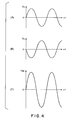
- Figs. 4(A) to 4(C) are graphs showing potentials measured at both ends of the plasma load and a composite potential thereof.
- Fig. 4(A) shows potential Va at one of the plasma electrodes 56A (point a)
- Fig. 4(B) shows potential Vb at the other plasma electrode 56B (point b).
- the neutral point i.e., zero point of the potential is around a half of the load in the plasma P, and this point corresponds to an imaginary grounded point.
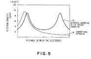
- Fig. 5 shows plasma densities between the plasma electrodes measured by a simulation.
- curve A shows distribution of the plasma density of a conventional apparatus while curve B shows the plasma density of an apparatus according to the present invention.
- the curve A of the conventional apparatus expresses only one peak of the plasma density around the electrode on the left side, i.e., the electrode in a hot state.
- the curve B of the apparatus of the present invention shows two peaks appearing respectively around both of the electrodes, thus enhancement of the plasma density can be confirmed over the whole range.
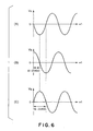
- Fig. 4(A) shows the same voltage wave form as that in Fig. 4(A)
- Fig. 6(B) shows a voltage wave form shifted in phase by 90 degrees relative to the wave form of Fig. 6(A)
- Fig. 6(C) shows a wave form shifted in phase by 180 degrees relative to the wave form of Fig. 6(A).
- the configuration of the present invention is not limited to this aspect, but at least one reactance element among the two capacitive reactance elements consisting of the capacitors C1, C2 and the two inductive reactance elements consisting of the coils L1, L2 may be variable.
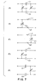
- the configuration of the high frequency matching circuit 74 is not limited to the one shown in Fig. 3, but may be configured as shown in Figs. 7, for example.
- Figs. 7 are circuit diagrams respectively showing modifications of the high frequency matching circuit.
- a circuit shown in Fig. 7(A) is configured to have a reversed connecting relation between the coils L1, L2 as the inductive reactance and the capacitors C1, C2 as the capacitive reactance.
- both the capacitors C1, C2 are connected in series with respective wires 60 extending from the load, while both the coils L1, L2 are connected in parallel with the wires across the capacitors C1, C2.
- both the coils L1, L2 are variable.
- a circuit shown in Fig. 7(B) is configured such that one of the capacitors connected in parallel with the load in the circuit shown in Fig. 3, i.e., the capacitor C1 which is positioned nearer to the load is removed to create an opened state.
- a circuit shown in Fig. 7(C) is configured such that the other one of the capacitors connected in parallel with the load in the circuit shown in Fig. 3, i.e., the capacitor C2 which is positioned farther from the load is removed to provide an opened state. In either case, the capacitor C2 or capacitor C1 is variable.
- a circuit shown in Fig. 7(D) is configured such that one of the coils connected in parallel with the load in the circuit shown in Fig.
- a circuit shown in Fig. 7(E) is configured such that the other one of the coils connected in parallel with the load in the circuit shown in Fig. 7(A), i.e., the coil L2 which is positioned farther from the load is removed to provide an opened state. In either case, the coil L2 or coil L1 is variable.
- the present invention is not limited to the film forming process, but may be applied to the plasma etching process, plasma ashing process or the like.
- the present invention is not limited to this aspect, but may be applied to a sheet-fed type plasma treating apparatus adapted to process semiconductor wafers, one for each operation.
- a susceptor which is a holding means of an object to be processed and is adapted to hold a semiconductor wafer placed thereon and a shower head portion adapted to supply processing gases including a plasma gas constitute both of the plasma electrodes.
- the object to be processed is not limited to semiconductor wafers, but this invention may also be applied to glass substrates or LCD substrates.
Landscapes
- Physics & Mathematics (AREA)
- Engineering & Computer Science (AREA)
- Plasma & Fusion (AREA)
- Chemical & Material Sciences (AREA)
- Analytical Chemistry (AREA)
- Chemical Vapour Deposition (AREA)
- Plasma Technology (AREA)
Abstract
A plasma treating apparatus adapted to provide a predetermined plasma treatment to an object W to be treated comprises a processing chamber 12 configured to be capable of being vacuumed, an object holding means 20 adapted to hold the object to be treated, a high frequency power source 58 adapted to generate high frequency voltage, a plasma gas supplying means 38 adapted to supply a plasma generating gas to be treated to generate plasma to the processing chamber, a pair of plasma electrodes 56, 56B connected to the output side of the high frequency power source via wirings 60 to generate plasma in the processing chamber, the pair of plasma electrodes being brought into an excited electrode state. In addition, a high frequency matching means 72 is provided in the middle of the wirings. In this case, each of the plasma electrodes 56A, 56B is not grounded. Thus, the plasma density can be increased, and the efficiency of generating plasma can be enhanced.
Description
- The present invention relates to a plasma treating apparatus for providing a plasma treatment, such as film forming or etching, to an object to be teated, such as a semiconductor wafer or the like.
- Generally, in order to produce semiconductor integrated circuits, various treatments including film forming, etching, oxidation, diffusion, modification and removal of naturally oxidized membranes are performed. In the case of performing these treatments in a vertical type, such as the so-called batch type heating apparatus, semiconductor wafers are transferred from a cassette capable of containing multiple sheets, for example 25 sheets, of semiconductor wafers onto a vertical type wafer boat, wherein the respective wafers are supported on the wafer boat in a multi-staged fashion. Depending on the wafer size, the wafer boat can contain 30 to 150 sheets of wafers. Thereafter, the wafer boat is loaded in a processing chamber from below, which chamber is capable of exhaustion, and the interior of the processing chamber is then kept airtight. Then, a predetermined heating treatment is performed while controlling various process conditions, such as flow rates of processing gases, processing pressure, processing temperature or the like.
- Recently, needs for more highly integrated and refined semiconductor integrated circuits have been increased, and reduction of heat history in the production process for semiconductor integrated circuits is also desired in view of enhancement of the properties of circuit elements. Under such circumstances, various processing apparatuses utilizing plasma have been proposed because of possibility to perform an intended treatment, even without subjecting wafers to a significantly high temperature, in a vertical batch type processing apparatus (e.g., see
Patent Documents
For example, in a conventional plasma treating apparatus, for example, a pair of electrodes are provided respectively opposed to the center of a cylindrical processing chamber able to be vacuumed, on the outside of a side wall of the processing chamber. One of the electrodes is connected with a high frequency power source for generating plasma, and the other electrode is grounded, so as to generate plasma in the whole interior of the processing chamber by applying a high frequency voltage between both the electrodes. The semiconductors wafers are supported in a multi-staged fashion at an approximately central portion in the processing chamber, and a gas nozzle adapted to introduce a gas used for generating, for example plasma, is arranged on one side of the wafers. Thus, the wafers can be subjected to a plasma treatment by a heater provided surrounding the outer periphery of the processing chamber while being maintained to be heated at a predetermined temperature. - Now, a high frequency circuit including the aforementioned high frequency power source will be described. Fig. 8 is a diagram showing an equivalent circuit for a conventional high frequency circuit including a high frequency power source. In Fig. 8,
reference numerals plasma electrodes frequency power source 6 of 13.56MHz, for example, viawirings 4. By applying a high frequency between theseplasma electrodes plasma electrodes high frequency electrode 6 as a load and can be expressed equivalently as a series circuit consisting of a capacitor C, a coil L and a resistance R. Either one of the two plasma electrodes, for example, thelower plasma electrode 2B in the drawing, is grounded.
In the middle of thewirings 4, a highfrequency matching circuit 8 is provided to perform matching of impedance in order to cancel a reflected wave from the load due to the plasma P, thereby to enhance efficiency of plasma generation. The highfrequency matching circuit 8 comprises a first variable capacitor C1 connected in series with theplasma electrode 2A, a first coil L1, and a second variable capacitor C2 connected in parallel with the load of the plasma P on the side of the highfrequency power source 6. It should be appreciated that the highfrequency matching circuit 8 in the connected state described above is generally referred to as an inversed L type matching circuit. - In the high
frequency matching circuit 8, by automatically adjusting the first and second variable capacitors C1, C2 to cancel the reflected wave on the side of the load of plasma P, the matching of impedance can be performed. As an alternative of the highfrequency matching circuit 8, for example as shown in Fig. 9(A), it may be constructed with the first and second variable capacitors C1, C2 respectively connected in series with the load of plasma P, and a first variable coil L2 connected with the connection point between the two variable capacitors C1, C2 as well as connected in parallel with the load of plasma P via theother wiring 4. Otherwise, as shown in Fig. 9(B), thefrequency matching circuit 8 may be constructed with a first and a second variable coils L2, L3 respectively connected in series with the load of plasma P, and a capacitor C3 connected with the connection point between the two variable coils L2, L3 as well as connected in parallel with the load of plasma P via theother wiring 4. It should be appreciated that the circuit construction as shown in Fig. 9 is generally referred to as a T type matching circuit. - Patent Document 1:
TOKUKAIHEI No. 3-224222
Patent Document 2:TOKUKAIHEI No. 5-251391
Patent Document 3:TOKUKAI No. 2002-280378
Patent Document 4:TOKUKAI No. 2001-44780
Patent Document 1:TOKUKAI No. 2003-264100 - Because the
plasma electrode 2B is grounded, a voltage Vab applied between both theplasma electrodes frequency matching circuit 8 described above is a sinusoidal wave as shown in Fig. 10.
In such a high frequency circuit, high production efficiency of highly powered plasma is required. However, in the high frequency circuit as described above, the plasma density to be obtained is not so high, thus the plasma production efficiency can not be enhanced sufficiently as desired. - In view of the above problems, the present invention was made to address them effectively. Therefore, it is an object of the present invention to provide a plasma treating apparatus which can increase the plasma density and enhance the plasma production efficiency.
- The present invention is a plasma treating apparatus adapted to provide a predetermined plasma treatment to an object to be treated, comprising: a processing chamber capable of being vacuumed; an object holding means adapted to hold the object; a high frequency power source adapted to generate high frequency voltage; a plasma gas supplying means adapted to supply a plasma generating gas to be treated to generate plasma to the processing chamber; a pair of plasma electrodes connected to the output side of the high frequency power source via wirings to generate plasma in the processing chamber, the pair of plasma electrodes being brought into an excited electrode state; and a high frequency matching means provided in the middle of the wirings and having impedance; wherein each plasma electrode is not grounded.
As described above, since the pair of plasma electrodes provided in the processing chamber are brought into an excited electrode state (or hot state), without grounding, by connecting them with an output side of the high frequency power source, the voltage to be applied to both the plasma electrodes can be significantly increased by properly adjusting the impedance, thus increasing the plasma density as well as enhancing the efficiency of generating plasma. - The present invention is the plasma treating apparatus, wherein the high frequency matching means includes one or more first reactance elements connected in parallel with a load of plasma between the plasma electrodes and having either one property of inductive reactance or capacitive reactance, and a plurality of second reactance elements connected in series with each plasma electrode and having another property than that of the first reactance elements.
- The present invention is the plasma treating apparatus, wherein at least either one of the first or second reactance elements is variable.
- The present invention is the plasma treating apparatus, wherein a detector for detecting the reflected wave generated on the side of the plasma electrodes is provided in the middle of the wirings between the high frequency matching means and the high frequency power source; and wherein the impedance of the high frequency matching means is controlled by a control unit based on a signal transmitted from the detector.
- The present invention is the plasma treating apparatus, wherein the control unit controls the impedance of the high frequency matching means such that the reflected wave generated on the side of the plasma electrodes becomes zero.
- The present invention is the plasma treating apparatus, wherein the first reactance elements comprise a pair of capacitors with variable capacitance; and wherein the second reactance elements comprise a pair of coils.
- The present invention is the plasma treating apparatus, wherein the first reactance elements comprise a pair of coils with variable inductance; and wherein the second reactance elements comprise a pair of capacitors.
- The present invention is the plasma treating apparatus, wherein the first reactance elements comprise a single capacitor with variable capacitance; and wherein the second reactance elements comprise a pair of coils.
- The present invention is the plasma treating apparatus, wherein the single capacitor is arranged in the wirings, on the side of the plasma electrodes with respect to the pair of coils.
- The present invention is the plasma treating apparatus, wherein the single capacitor is arranged in the wirings, opposite to the plasma electrodes with respect to the pair of coils.
- The present invention is the plasma treating apparatus, wherein the first reactance elements comprise a single coil with variable inductance; and wherein the second reactance elements comprise a pair of capacitors.
- The present invention is the plasma treating apparatus, wherein the single coil is arranged in the wirings, on the side of the plasma electrodes with respect to the pair of capacitors.
- The present invention is the plasma treating apparatus, wherein the single coil is arranged in the wirings, opposite to the plasma electrodes with respect to the pair of capacitors.
- The present invention is the plasma treating apparatus, wherein the processing chamber is a vertical type processing chamber which can contain multiple sheets of the objects to be treated.
- The present invention is the plasma treating apparatus, wherein the processing chamber is a sheet-fed type processing chamber which can contain one sheet of the object to be treated for each operation.
- As discussed above, according to the plasma processing chamber of the present invention, the following outstanding effects can be provided.
Since the pair of plasma electrodes provided in the processing chamber are brought into an excited electrode state (or hot state), without grounding, by connecting them with an output side of the high frequency power source, the voltage to be applied to both the plasma electrodes can be significantly increased by properly adjusting the impedance, as such increasing the plasma density as well as enhancing the efficiency of generating plasma. -
- Fig. 1 is a longitudinal section for illustrating a construction of one example of a plasma treating apparatus according to the present invention.
- Fig. 2 is a transverse section illustrating a plasma treating apparatus.
- Fig. 3 shows an equivalent circuit of a high frequency circuit connected with a high frequency power source.
- Figs. 4(A) to 4(C) are graphs showing potentials measured at both ends of the plasma load and a composite potential thereof.
- Fig. 5 is a graph showing distribution of the plasma density of a conventional apparatus and an apparatus according to the present invention.
- Figs. 6(A) to 6(C) are graphs showing changes of the phase difference of the voltage wave form.
- Figs. 7(A) to 7(E) respectively show circuit diagrams as alternatives of a high frequency matching circuit.
- Fig. 8 shows an equivalent circuit of a conventional high frequency circuit including a high frequency power source.
- Figs. 9(A) and 9(B) are diagrams for illustrating other constructions of the conventional high frequency matching circuit.
- Fig. 10 shows a voltage wave form applied to both of the plasma electrodes due to the conventional high frequency matching circuit.
- Hereinafter, one example of a plasma treating apparatus according to the present invention will be described with reference to attached drawings.
Fig. 1 is a longitudinal section for illustrating one example a plasma treating apparatus according to the present invention. Fig. 2 is a transverse section illustrating the plasma treating apparatus (a heating means is not shown in the drawing). Fig. 3 shows an equivalent circuit of a high frequency circuit connected with a high frequency power source. Now, an example in which an ammonia gas is used as a plasma generating gas and a silicon nitride (SiN) film is formed by the plasma CVD using a hexachlorodisilane gas (hereinafter, referred to as a "HCD" gas) as a film forming gas will be described.
As shown in the drawings, aplasma treating apparatus 10 includes acylindrical processing chamber 12 with a ceiling having an opening formed at its bottom end. The entire body of theprocessing chamber 12 is formed of, for example quartz, and aquartz ceiling plate 14 is provided at the ceiling of the interior of theprocessing chamber 12 to seal the interior. A manifold 16 which is formed from, for example stainless steel, into a cylindrical body is coupled to the bottom end opening of theprocessing chamber 12 via a sealingmember 18, such as an O-ring. - The bottom end of the
processing chamber 12 is supported by the manifold 16, and awafer boat 20 formed of quartz can be inserted and retracted vertically from below themanifold 16. Thewafer boat 20 serves as a holding means for holding objects to be treated, on which multiple sheets of semiconductor wafers W as the objects to be treated are placed in a multi-staged fashion. In this example, struts 20A of thewafer boat 20 are designed to support, for example, 30 sheets of wafers each having a 300mm diameter, at an approximately equal pitch, in a multi-staged fashion.
Thewafer boat 20 is mounted on a table 24 via aheat insulating cylinder 22 made of quartz, and the table 24 is supported on arotary shaft 28 extending through acover 26 formed of, for example, stainless steel, which serves to open and close the bottom end of the manifold 16.
In the portion that therotary shaft 28 extends through, a magnetic fluid seal is provided so as to seal therotary shaft 28 airtightly and support it rotatably. A sealingmember 32 made of, for example, an O-ring is provided at the periphery of thecover 26 and the bottom end of the manifold 16 so as to keep the interior of the chamber in a sealed state. - The
rotary shaft 28 is attached to a distal end of anarm 36 supported by alifting mechanism 34, such as a boat elevator, and is configured to lift and lower or insert and retract thewafer boat 20 and cover 26 integrally, relative to the interior of theprocessing chamber 12. It is noted that the table 24 may be fixed to thecover 26, and that the treatment for the wafers W may be performed without rotating thewafer boat 20.
In the manifold 16, a plasma gas supplying means 38 for supplying a plasma generating gas to be treated to generate plasma, for example, an ammonia (NH3) gas into theprocessing chamber 12, and a film forming gas supplying means 40 for supplying a film forming gas, for example, an HCD gas as a silane-based gas into thechamber 12 are provided. Specifically, the plasma gas supplying means 38 has a plasmagas dispersing nozzle 42 formed of a quartz tube, which extends into and through a side wall of the manifold 16 and bending upward. In the plasmagas dispersing nozzle 42, a plurality of (multiple)gas injecting apertures 42A are formed along the length of thenozzle 42 and spaced apart from each other at a predetermined interval so that the ammonia gas can be injected, in a substantially uniform manner, horizontally from eachgas injecting aperture 42A. - Similarly, the film forming gas supplying means 40 has also film forming
gas dispersing nozzles 44 each formed of a quartz tube, extending into and though a side wall of the manifold 16 and bending upward. In this example, two film forminggas dispersing nozzles 44 are provided (see Fig. 2). In each film forminggas dispersing nozzle 44, a plurality of (multiple) gas injecting apertures 44A are formed along the length of thenozzle 44 and spaced apart from each other at a predetermined interval so that the silane-based gas can be injected, in a substantially uniform manner, horizontally from each gas injecting aperture 44A.
At a portion of a side wall of theprocessing chamber 12, aplasma generator 48 is provided along the vertical direction, and anelongated exhaust hole 50 is provided, for example, by cutting off a portion of a side wall of theprocessing chamber 12 on the opposite side of theplasma generator 48 across theprocessing chamber 12. Theexhaust hole 50 serves to discharge, due to vacuum, an ambient gas in the interior of theprocessing chamber 12.
Specifically, theplasma generator 48 is formed to be integrated with the chamber by forming a vertically elongated opening 52 by cutting off a portion of a side wall of theprocessing chamber 12 along the vertical direction in a predetermined width, and by welding and joining airtightly a vertically elongatedplasma partition wall 54 formed of, for example quartz and having a concave cross section to the outer wall of the chamber such that thepartition wall 54 can cover the opening 52 from the outside. In such a way, by deforming a portion of the side wall of theprocessing chamber 12 outside to have a concave cross section, aplasma generator 48 which is opened to and in communication with the interior of theprocessing chamber 12 at its one side can be formed. Namely, the space in the interior of theplasma generator 48 is integrally communicating with the interior of theprocessing chamber 12. The opening 52 is formed to have a vertical length sufficient to cover all of the wafers W held by thewafer boat 20 in the vertical direction. - On outer surfaces of both side walls of the
plasma partition wall 54, a pair ofelongated plasma electrodes plasma electrodes frequency power source 58 for generating plasma is connected viawirings 60 so as to generate plasma by applying a high frequency voltage of, for example 13.56MHz, to theplasma electrodes
The plasmagas dispersing nozzle 42 extending upward in theprocessing chamber 12 is bent radially outward in the middle of the extension in theprocessing chamber 12, directed at the most back portion (the farthest portion from the center of the processing chamber 12) in theplasma generator 48, and raised upward along the most back portion. Accordingly, the ammonia gas injected from thegas injecting apertures 42A of the plasmagas dispersing nozzle 42 is decomposed or otherwise activated by plasma so as to flow toward the center of theprocessing chamber 12 while being dispersed. - On the outside of the
plasma partition wall 54, aninsulation protecting cover 62 formed of, for example quartz, is attached such that theinsulation protecting cover 62 covers theplasma partition wall 54. Again, on the outside of theinsulation protecting cover 62, ashield 64 is provided in order to cover the protectingcover 62 and prevent leakage of high frequency plasma. In this case, the shield is grounded.
The two film forminggas dispersing nozzles 44 are provided, while being raised, in the vicinity of the outside of the opening 52 of theplasma generator 48, i.e., on both outsides of the opening 52 (in the processing chamber 12), such that a silane-based gas can be injected toward the center of theprocessing chamber 12 from each gas injecting aperture 44A provided in thegas dispersing nozzles 44. - At the
exhaust hole 50 provided opposing to theplasma generator 48, an exhausthole covering member 66 which is formed of quartz and molded to have an U-shaped cross section is attached by welding to cover theexhaust hole 50. The exhausthole covering member 66 extends upward along the side wall of theprocessing chamber 12 and is configured to be vacuumed by a vacuum exhausting system provided with a vacuum pump or the like (not shown) via an upper gas exit 68. A cylindrical heating means 70 is provided surrounding the outer periphery of theprocessing chamber 12 so as to heat theprocessing chamber 12 and wafers W placed therein.
A high frequency matching means 72 which is one of features of the present invention is provided in the middle of thewirings 60 respectively connecting the highfrequency power source 58 with both theplasma electrodes plasma electrodes frequency power source 58 via thewirings 60 without being grounded, as such creating an excited electrode state, i.e., a hot state. The high frequency matching means 72 is composed of a highfrequency matching circuit 74 provided in thewirings 60, awave detector 76 connected in parallel with the highfrequency matching circuit 74 and adapted to detect a reflected wave generated on the side of theplasma electrodes control unit 78 adapted to adjust and control impedance of the highfrequency matching circuit 74 based on an output from thewave detector 76 and including, for example a microcomputer, or the like. An equivalent circuit for a high frequency circuit in this case is shown in Fig. 3. - In Fig. 3, the plasma P generated between the
plasma electrodes frequency power source 58, and the plasma P can be equivalently expressed as a series circuit composed of a capacitor C, a coil L and a resistance R. The highfrequency matching circuit 74 is composed of two coils L1, L2 respectively connected in series with theplasma electrodes plasma electrodes plasma electrodes - Next, a plasma treating method which is performed by using the plasma treating apparatus as constructed described above will be discussed. As a plasma treatment, a case of subjecting the wafer surface to plasma CVD so as to form a silicon nitride film will be described.
First, thewafer boat 20 on which multiple sheets, for example 50 sheets, of wafers each having a 300mm diameter are placed at a normal temperature, is loaded in theprocessing chamber 12 set at a predetermined temperature by lifting thewafer boat 20 from below, and the interior of theprocessing chamber 12 is then sealed by closing the bottom opening of the manifold 16 due to thecover 26.
Thereafter, the interior of theprocessing chamber 12 is kept at a predetermined processing pressure by providing vacuum thereto, while the electric power to be applied to the heating means 70 is increased. In this way, the wafer temperature is elevated to maintain a processing temperature. In addition, various types of processing gases are supplied alternately and intermittently from the plasmagas supplying means 38 and film forming gas supplying means 40 so as to form a silicon nitride film on a surface of each wafer W supported on therotating wafer boat 20. - Specifically, the NH3 gas is injected horizontally from each
gas injecting aperture 42A of the plasmagas dispersing nozzle 42 provided in theplasma gas generator 48, while the HCD gas as the film forming gas is injected horizontally from each gas injecting aperture 44A of the film forminggas dispersing nozzle 44, thus both of the gases react with each other so as to form a silicon nitride film. In this case, a high frequency voltage generated from the highfrequency power source 58 is applied between theplasma electrodes plasma generator 48. In this way, the NH3 gas injected from the gas injecting apertures 44A of the plasmagas dispersing nozzle 44 flows in a space between theplasma electrodes processing chamber 12 from the opening 52 of theplasma generator 48, thus flowing in a laminar flow state between the wafers W. Consequently, each radical reacts with molecules of the HCD gas attached to the surface of each wafer W, thus forming a silicon nitride film as described above. - During the film forming operation as described above, the reflected wave from the plasma P is detected by the
wave detector 76 as shown in Figs. 2 and 3, and thecontrol unit 78 automatically controls the impedance of the highfrequency matching circuit 74 such that the reflected wave becomes "zero", thereby performing the matching. In the case shown in Fig. 3, the values of the respective capacitors C1, C2 are suitably adjusted. For example, if the impedance of the load due to the plasma P is "a + jb", thecontrol unit 78 adjusts the load of the highfrequency matching circuit 74 and plasma P at "50Ω".
When the impedance is matched as described above, assuming that the composite impedance of the capacitors C1, C2 is "-j/(ωC)" and that the impedances of the coils L1, L2 are "+jωL1" and "+jωL2", respectively, the imaginary number part becomes zero, thereby obtaining the following equation.

Accordingly, the potentials at both ends of the load in the plasma P, i.e., the potentials at theplasma electrode 56A (point a) andplasma electrode 56B (point b) are shifted in phase by 180 degrees as shown in Figs. 4(A) and 4(B). - Figs. 4(A) to 4(C) are graphs showing potentials measured at both ends of the plasma load and a composite potential thereof. Fig. 4(A) shows potential Va at one of the
plasma electrodes 56A (point a), and Fig. 4(B) shows potential Vb at theother plasma electrode 56B (point b). Accordingly, the neutral point, i.e., zero point of the potential is around a half of the load in the plasma P, and this point corresponds to an imaginary grounded point. As a result, the difference of potentials Vab (=Va - Vb) between both of theelectrodes
As described above, by bringing both of theelectrodes electrodes - As discussed above, by bringing both of the
electrodes plasma electrodes
Fig. 5 shows plasma densities between the plasma electrodes measured by a simulation. In Fig. 5, curve A shows distribution of the plasma density of a conventional apparatus while curve B shows the plasma density of an apparatus according to the present invention. As shown in Fig. 5, the curve A of the conventional apparatus expresses only one peak of the plasma density around the electrode on the left side, i.e., the electrode in a hot state. On the contrary, the curve B of the apparatus of the present invention shows two peaks appearing respectively around both of the electrodes, thus enhancement of the plasma density can be confirmed over the whole range. - As shown in Figs. 4(A) and 4(B), while the voltage wave form shown in Fig. 4(B) is shifted in phase by 180 degrees relative to the voltage wave form in Fig. 4(A), the potential difference of the voltage wave form shown in Fig. 4(B) can be adjusted by suitably modifying the variable capacitors C1, C2 shown in Fig. 1. Fig. 6(A) shows the same voltage wave form as that in Fig. 4(A), Fig. 6(B) shows a voltage wave form shifted in phase by 90 degrees relative to the wave form of Fig. 6(A), and Fig. 6(C) shows a wave form shifted in phase by 180 degrees relative to the wave form of Fig. 6(A).
In this way, since the phase of voltage between theplasma electrodes
It is noted that while both of the capacitors C1, C2 are variable in the apparatus shown in Fig. 1, the configuration of the present invention is not limited to this aspect, but at least one reactance element among the two capacitive reactance elements consisting of the capacitors C1, C2 and the two inductive reactance elements consisting of the coils L1, L2 may be variable. - The configuration of the high
frequency matching circuit 74 is not limited to the one shown in Fig. 3, but may be configured as shown in Figs. 7, for example. Figs. 7 are circuit diagrams respectively showing modifications of the high frequency matching circuit. A circuit shown in Fig. 7(A) is configured to have a reversed connecting relation between the coils L1, L2 as the inductive reactance and the capacitors C1, C2 as the capacitive reactance. In the configuration, both the capacitors C1, C2 are connected in series withrespective wires 60 extending from the load, while both the coils L1, L2 are connected in parallel with the wires across the capacitors C1, C2. In this case, both the coils L1, L2 are variable.
A circuit shown in Fig. 7(B) is configured such that one of the capacitors connected in parallel with the load in the circuit shown in Fig. 3, i.e., the capacitor C1 which is positioned nearer to the load is removed to create an opened state. A circuit shown in Fig. 7(C) is configured such that the other one of the capacitors connected in parallel with the load in the circuit shown in Fig. 3, i.e., the capacitor C2 which is positioned farther from the load is removed to provide an opened state. In either case, the capacitor C2 or capacitor C1 is variable.
A circuit shown in Fig. 7(D) is configured such that one of the coils connected in parallel with the load in the circuit shown in Fig. 7(A), i.e., the coil L1 which is positioned nearer to the load is removed to create an opened state. A circuit shown in Fig. 7(E) is configured such that the other one of the coils connected in parallel with the load in the circuit shown in Fig. 7(A), i.e., the coil L2 which is positioned farther from the load is removed to provide an opened state. In either case, the coil L2 or coil L1 is variable. - While an example of the film forming process for a silicon nitride film has been described above, other film forming processes for other types of films may be used. In addition, the present invention is not limited to the film forming process, but may be applied to the plasma etching process, plasma ashing process or the like.
Furthermore, while an example of a vertical batch type plasma treating apparatus which can process multiple sheets of semiconductor wafers at a time has been described, the present invention is not limited to this aspect, but may be applied to a sheet-fed type plasma treating apparatus adapted to process semiconductor wafers, one for each operation. In this case, a susceptor which is a holding means of an object to be processed and is adapted to hold a semiconductor wafer placed thereon and a shower head portion adapted to supply processing gases including a plasma gas constitute both of the plasma electrodes.
The object to be processed is not limited to semiconductor wafers, but this invention may also be applied to glass substrates or LCD substrates.
Claims (15)
- A plasma treating apparatus adapted to provide a predetermined plasma treatment to an object to be treated, comprising:a processing chamber capable of being vacuumed;an object holding means adapted to hold an object;a high frequency power source adapted to generate high frequency voltage;a plasma gas supplying means adapted to supply a plasma generating gas to be treated to generate plasma to the processing chamber;a pair of plasma electrodes connected to the output side of the high frequency power source via wirings to generate plasma in the processing chamber, the pair of plasma electrodes being brought into an excited electrode state; anda high frequency matching means provided in the middle of the wirings and having impedance;wherein each plasma electrode is not grounded.
- The plasma treating apparatus according to claim 1,
wherein the high frequency matching means includes one or more first reactance elements connected in parallel with a load of plasma between the plasma electrodes and having either one property of inductive reactance or capacitive reactance, and a plurality of second reactance elements connected in series with each plasma electrode and having another property than that of the first reactance elements. - The plasma treating apparatus according to claim 2,
wherein at least either one of the first or second reactance elements is variable. - The plasma treating apparatus according to claim 1,
wherein a detector for detecting the reflected wave generated on the side of the plasma electrodes is provided in the middle of the wirings between the high frequency matching means and the high frequency power source; and
wherein the impedance of the high frequency matching means is controlled by a control unit based on a signal transmitted from the detector. - The plasma treating apparatus according to claim 4,
wherein the control unit controls the impedance of the high frequency matching means such that the reflected wave generated on the side of the plasma electrodes becomes zero. - The plasma treating apparatus according to claim 3,
wherein the first reactance elements comprise a pair of capacitors with variable capacitance; and
wherein the second reactance elements comprise a pair of coils. - The plasma treating apparatus according to claim 3,
wherein the first reactance elements comprise a pair of coils with variable inductance; and
wherein the second reactance elements comprise a pair of capacitors. - The plasma treating apparatus according to claim 3,
wherein the first reactance elements comprise a single capacitor with variable capacitance; and
wherein the second reactance elements comprise a pair of coils. - The plasma treating apparatus according to claim 8,
wherein the single capacitor is arranged in the wirings, on the side of the plasma electrodes with respect to the pair of coils. - The plasma treating apparatus according to claim 8,
wherein the single capacitor is arranged in the wirings, opposite to the plasma electrodes with respect to the pair of coils. - The plasma treating apparatus according to claim 3,
wherein the first reactance elements comprise a single coil with variable inductance; and
wherein the second reactance elements comprise a pair of capacitors. - The plasma treating apparatus according to claim 11,
wherein the single coil is arranged in the wirings, on the side of the plasma electrodes with respect to the pair of capacitors. - The plasma treating apparatus according to claim 11,
wherein the single coil is arranged in the wirings, opposite to the plasma electrodes with respect to the pair of capacitors. - The plasma treating apparatus according to claim 1,
wherein the processing chamber is a vertical type processing chamber which can contain multiple sheets of the objects to be treated. - The plasma treating apparatus according to claim 1,
wherein the processing chamber is a sheet-fed type processing chamber which can contain one sheet of the object to be treated for each operation.
Applications Claiming Priority (2)
| Application Number | Priority Date | Filing Date | Title |
|---|---|---|---|
| JP2004257994A JP4344886B2 (en) | 2004-09-06 | 2004-09-06 | Plasma processing equipment |
| PCT/JP2005/015767 WO2006027972A1 (en) | 2004-09-06 | 2005-08-30 | Plasma processing apparatus |
Publications (2)
| Publication Number | Publication Date |
|---|---|
| EP1791172A1 true EP1791172A1 (en) | 2007-05-30 |
| EP1791172A4 EP1791172A4 (en) | 2009-01-28 |
Family
ID=36036258
Family Applications (1)
| Application Number | Title | Priority Date | Filing Date |
|---|---|---|---|
| EP05776943A Withdrawn EP1791172A4 (en) | 2004-09-06 | 2005-08-30 | PLASMA TREATMENT APPARATUS |
Country Status (7)
| Country | Link |
|---|---|
| US (1) | US8267041B2 (en) |
| EP (1) | EP1791172A4 (en) |
| JP (1) | JP4344886B2 (en) |
| KR (1) | KR100955359B1 (en) |
| CN (1) | CN100474526C (en) |
| TW (1) | TWI402911B (en) |
| WO (1) | WO2006027972A1 (en) |
Cited By (1)
| Publication number | Priority date | Publication date | Assignee | Title |
|---|---|---|---|---|
| WO2017017407A1 (en) * | 2015-07-24 | 2017-02-02 | C-Tech Innovation Limited | Radio frequency heating system |
Families Citing this family (20)
| Publication number | Priority date | Publication date | Assignee | Title |
|---|---|---|---|---|
| JP4344886B2 (en) * | 2004-09-06 | 2009-10-14 | 東京エレクトロン株式会社 | Plasma processing equipment |
| KR100876050B1 (en) | 2004-12-28 | 2008-12-26 | 가부시키가이샤 히다치 고쿠사이 덴키 | Substrate processing equipment |
| JP4470970B2 (en) * | 2007-07-31 | 2010-06-02 | 東京エレクトロン株式会社 | Plasma processing equipment |
| US20090056877A1 (en) | 2007-08-31 | 2009-03-05 | Tokyo Electron Limited | Plasma processing apparatus |
| JP5098882B2 (en) * | 2007-08-31 | 2012-12-12 | 東京エレクトロン株式会社 | Plasma processing equipment |
| JP5423205B2 (en) * | 2008-08-29 | 2014-02-19 | 東京エレクトロン株式会社 | Deposition equipment |
| GB0823565D0 (en) * | 2008-12-24 | 2009-01-28 | Oxford Instr Plasma Technology | Signal generating system |
| JP5099101B2 (en) * | 2009-01-23 | 2012-12-12 | 東京エレクトロン株式会社 | Plasma processing equipment |
| JP5136574B2 (en) | 2009-05-01 | 2013-02-06 | 東京エレクトロン株式会社 | Plasma processing apparatus and plasma processing method |
| CN102142388A (en) * | 2010-12-10 | 2011-08-03 | 北京七星华创电子股份有限公司 | Vertical boat supporting piece for heat-treatment equipment of semiconductor |
| US10058626B2 (en) * | 2012-05-28 | 2018-08-28 | Saraya Co., Ltd. | Sterilization device and sterilization method using same |
| EP3322258A4 (en) * | 2015-07-03 | 2019-03-27 | Toyo Seikan Group Holdings, Ltd. | HIGH FREQUENCY DIELECTRIC HEATING DEVICE |
| KR102146600B1 (en) * | 2016-08-01 | 2020-08-20 | 도쿄엘렉트론가부시키가이샤 | Substrate processing apparatus and substrate processing method |
| JP7489894B2 (en) * | 2020-10-20 | 2024-05-24 | 東京エレクトロン株式会社 | Plasma generating device, plasma processing device, and plasma processing method |
| US12413148B2 (en) * | 2021-05-20 | 2025-09-09 | Kaufman & Robinson, Inc. | Power efficient load current derived switch timing of switching resonant topology |
| US11823867B2 (en) * | 2021-05-20 | 2023-11-21 | Kaufman & Robinson, Inc. | Load current derived switch timing of switching resonant topology |
| JP7740822B2 (en) * | 2021-08-11 | 2025-09-17 | 東京エレクトロン株式会社 | Plasma processing apparatus and film forming method |
| JP7740840B2 (en) * | 2022-01-25 | 2025-09-17 | 東京エレクトロン株式会社 | Ignition control method, film formation method and film formation apparatus |
| JP2024166825A (en) * | 2023-05-19 | 2024-11-29 | 東京エレクトロン株式会社 | Plasma Processing Equipment |
| CN116618384A (en) * | 2023-05-29 | 2023-08-22 | 湖南红太阳光电科技有限公司 | A kind of vertical graphite boat cleaning equipment and cleaning method |
Family Cites Families (84)
| Publication number | Priority date | Publication date | Assignee | Title |
|---|---|---|---|---|
| US3704219A (en) * | 1971-04-07 | 1972-11-28 | Mcdowell Electronics Inc | Impedance matching network for use with sputtering apparatus |
| JPS60169139A (en) * | 1984-02-13 | 1985-09-02 | Canon Inc | Gas phase method equipment |
| US4557819A (en) * | 1984-07-20 | 1985-12-10 | Varian Associates, Inc. | System for igniting and controlling a wafer processing plasma |
| US4763087A (en) * | 1986-05-27 | 1988-08-09 | Schrader Paul D | Impedance matching network |
| US4956582A (en) * | 1988-04-19 | 1990-09-11 | The Boeing Company | Low temperature plasma generator with minimal RF emissions |
| US5178682A (en) * | 1988-06-21 | 1993-01-12 | Mitsubishi Denki Kabushiki Kaisha | Method for forming a thin layer on a semiconductor substrate and apparatus therefor |
| JPH03224222A (en) | 1988-10-31 | 1991-10-03 | Tokyo Electron Ltd | Film formation |
| JPH02159027A (en) * | 1988-12-13 | 1990-06-19 | Tel Sagami Ltd | Plasma treatment device |
| JPH0327120A (en) | 1989-06-20 | 1991-02-05 | Tonen Corp | Silicon nitride inorganic fiber |
| DE3923661A1 (en) * | 1989-07-18 | 1991-01-24 | Leybold Ag | CIRCUIT ARRANGEMENT FOR ADJUSTING THE IMPEDANCE OF A PLASMA LINE TO A HIGH FREQUENCY GENERATOR |
| JPH0327120U (en) * | 1989-07-26 | 1991-03-19 | ||
| JPH03277774A (en) * | 1990-03-27 | 1991-12-09 | Semiconductor Energy Lab Co Ltd | Photo-vapor reaction device |
| DE69133169D1 (en) * | 1990-05-09 | 2003-01-16 | Canon Kk | Method for creating a structure and method for preparing a semiconducting device using this method |
| US5195045A (en) * | 1991-02-27 | 1993-03-16 | Astec America, Inc. | Automatic impedance matching apparatus and method |
| JPH0531735A (en) * | 1991-08-02 | 1993-02-09 | Canon Inc | Apparatus for molding optical element |
| US5298939A (en) * | 1991-11-04 | 1994-03-29 | Swanson Paul A | Method and apparatus for transfer of a reticle pattern onto a substrate by scanning |
| JP2934084B2 (en) * | 1991-11-25 | 1999-08-16 | キヤノン株式会社 | Molding equipment |
| JPH05251391A (en) * | 1992-03-04 | 1993-09-28 | Tokyo Electron Tohoku Kk | Plasma processing device for semiconductor wafer |
| WO1993021685A1 (en) * | 1992-04-16 | 1993-10-28 | Advanced Energy Industries, Inc. | Stabilizer for switch-mode powered rf plasma processing |
| US5339198A (en) * | 1992-10-16 | 1994-08-16 | The Dow Chemical Company | All-polymeric cold mirror |
| US7097712B1 (en) * | 1992-12-04 | 2006-08-29 | Semiconductor Energy Laboratory Co., Ltd. | Apparatus for processing a semiconductor |
| US5387842A (en) * | 1993-05-28 | 1995-02-07 | The University Of Tennessee Research Corp. | Steady-state, glow discharge plasma |
| US5414324A (en) * | 1993-05-28 | 1995-05-09 | The University Of Tennessee Research Corporation | One atmosphere, uniform glow discharge plasma |
| JPH077221A (en) * | 1993-06-18 | 1995-01-10 | Furukawa Electric Co Ltd:The | Semiconductor laser device |
| US5407524A (en) * | 1993-08-13 | 1995-04-18 | Lsi Logic Corporation | End-point detection in plasma etching by monitoring radio frequency matching network |
| US5556549A (en) * | 1994-05-02 | 1996-09-17 | Lsi Logic Corporation | Power control and delivery in plasma processing equipment |
| US6015503A (en) * | 1994-06-14 | 2000-01-18 | Fsi International, Inc. | Method and apparatus for surface conditioning |
| US5474648A (en) * | 1994-07-29 | 1995-12-12 | Lsi Logic Corporation | Uniform and repeatable plasma processing |
| EP0715334B1 (en) * | 1994-11-30 | 1999-04-14 | Applied Materials, Inc. | Plasma reactors for processing semiconductor wafers |
| US5876663A (en) * | 1995-11-14 | 1999-03-02 | The University Of Tennessee Research Corporation | Sterilization of liquids using plasma glow discharge |
| US7025831B1 (en) * | 1995-12-21 | 2006-04-11 | Fsi International, Inc. | Apparatus for surface conditioning |
| US5689215A (en) * | 1996-05-23 | 1997-11-18 | Lam Research Corporation | Method of and apparatus for controlling reactive impedances of a matching network connected between an RF source and an RF plasma processor |
| US7004107B1 (en) * | 1997-12-01 | 2006-02-28 | Applied Materials Inc. | Method and apparatus for monitoring and adjusting chamber impedance |
| JP3501668B2 (en) * | 1997-12-10 | 2004-03-02 | キヤノン株式会社 | Plasma CVD method and plasma CVD apparatus |
| US6273022B1 (en) * | 1998-03-14 | 2001-08-14 | Applied Materials, Inc. | Distributed inductively-coupled plasma source |
| US6232248B1 (en) * | 1998-07-03 | 2001-05-15 | Tokyo Electron Limited | Single-substrate-heat-processing method for performing reformation and crystallization |
| US6239018B1 (en) * | 1999-02-01 | 2001-05-29 | United Microelectronics Corp. | Method for forming dielectric layers |
| JP2000299198A (en) * | 1999-02-10 | 2000-10-24 | Tokyo Electron Ltd | Plasma processing equipment |
| EP1171946B1 (en) * | 1999-03-23 | 2006-08-30 | Advanced Energy Industries, Inc. | High frequency switch-mode dc powered computer system |
| JP2001104776A (en) * | 1999-10-06 | 2001-04-17 | Tokyo Electron Ltd | Processing device and processing method |
| KR100613674B1 (en) * | 1999-05-14 | 2006-08-21 | 동경 엘렉트론 주식회사 | Wafer processing apparatus and processing method |
| JP2001016063A (en) * | 1999-06-30 | 2001-01-19 | Aichi Electronic Co Ltd | Branching and distributing unit for high frequency |
| US6376387B2 (en) * | 1999-07-09 | 2002-04-23 | Applied Materials, Inc. | Method of sealing an epitaxial silicon layer on a substrate |
| CN1241316C (en) * | 1999-07-13 | 2006-02-08 | 东京电子株式会社 | RF power supply for generating inductively coupled plasma |
| JP4652499B2 (en) * | 1999-07-29 | 2011-03-16 | 株式会社ダイヘン | Impedance automatic matching method and matching device |
| KR100338057B1 (en) * | 1999-08-26 | 2002-05-24 | 황 철 주 | Antenna device for generating inductively coupled plasma |
| JP4731694B2 (en) * | 2000-07-21 | 2011-07-27 | 東京エレクトロン株式会社 | Semiconductor device manufacturing method and substrate processing apparatus |
| JP3911555B2 (en) | 2000-08-15 | 2007-05-09 | 独立行政法人産業技術総合研究所 | Silicon-based thin film manufacturing method |
| JP3979849B2 (en) | 2001-01-11 | 2007-09-19 | 株式会社日立国際電気 | Plasma processing apparatus and semiconductor device manufacturing method |
| JP4727057B2 (en) * | 2001-03-28 | 2011-07-20 | 忠弘 大見 | Plasma processing equipment |
| US6583572B2 (en) * | 2001-03-30 | 2003-06-24 | Lam Research Corporation | Inductive plasma processor including current sensor for plasma excitation coil |
| JP4682456B2 (en) * | 2001-06-18 | 2011-05-11 | 株式会社日立ハイテクノロジーズ | Substrate processing method and substrate processing apparatus |
| TW200300649A (en) * | 2001-11-27 | 2003-06-01 | Alps Electric Co Ltd | Plasma processing apparatus, its driving method, matching circuit design system, and plasma processing method |
| JP3574104B2 (en) | 2001-11-27 | 2004-10-06 | 三容真空工業株式会社 | Plasma generation driving device using matching circuit for plasma generation |
| JP4149243B2 (en) | 2001-11-30 | 2008-09-10 | アルプス電気株式会社 | Plasma processing apparatus and matching circuit design system for plasma processing apparatus |
| JP4132016B2 (en) * | 2001-12-25 | 2008-08-13 | 松下電器産業株式会社 | Matching circuit and plasma processing apparatus |
| US20030164143A1 (en) * | 2002-01-10 | 2003-09-04 | Hitachi Kokusai Electric Inc. | Batch-type remote plasma processing apparatus |
| TWI239794B (en) * | 2002-01-30 | 2005-09-11 | Alps Electric Co Ltd | Plasma processing apparatus and method |
| JP4414765B2 (en) * | 2002-02-20 | 2010-02-10 | パナソニック電工株式会社 | Plasma processing apparatus and plasma processing method |
| JP2003298378A (en) | 2002-04-04 | 2003-10-17 | Nihon Koshuha Co Ltd | Automatic matching device |
| JP2003323997A (en) * | 2002-04-30 | 2003-11-14 | Lam Research Kk | Plasma stabilizing method and plasma device |
| US6819052B2 (en) * | 2002-05-31 | 2004-11-16 | Nagano Japan Radio Co., Ltd. | Coaxial type impedance matching device and impedance detecting method for plasma generation |
| US6774569B2 (en) | 2002-07-11 | 2004-08-10 | Fuji Photo Film B.V. | Apparatus for producing and sustaining a glow discharge plasma under atmospheric conditions |
| US6876155B2 (en) * | 2002-12-31 | 2005-04-05 | Lam Research Corporation | Plasma processor apparatus and method, and antenna |
| US7767056B2 (en) * | 2003-01-14 | 2010-08-03 | Canon Anelva Corporation | High-frequency plasma processing apparatus |
| KR100771800B1 (en) * | 2003-01-24 | 2007-10-30 | 도쿄 엘렉트론 가부시키가이샤 | Method of cvd for forming silicon nitride film on substrate |
| US20040173314A1 (en) * | 2003-03-05 | 2004-09-09 | Ryoji Nishio | Plasma processing apparatus and method |
| TWI236055B (en) * | 2003-09-05 | 2005-07-11 | United Microelectronics Corp | Plasma apparatus and method capable of adaptive impedance matching |
| US7264676B2 (en) * | 2003-09-11 | 2007-09-04 | United Microelectronics Corp. | Plasma apparatus and method capable of adaptive impedance matching |
| US7157857B2 (en) * | 2003-12-19 | 2007-01-02 | Advanced Energy Industries, Inc. | Stabilizing plasma and generator interactions |
| US7326872B2 (en) * | 2004-04-28 | 2008-02-05 | Applied Materials, Inc. | Multi-frequency dynamic dummy load and method for testing plasma reactor multi-frequency impedance match networks |
| US7169256B2 (en) * | 2004-05-28 | 2007-01-30 | Lam Research Corporation | Plasma processor with electrode responsive to multiple RF frequencies |
| JP4344886B2 (en) * | 2004-09-06 | 2009-10-14 | 東京エレクトロン株式会社 | Plasma processing equipment |
| JP4975291B2 (en) * | 2004-11-09 | 2012-07-11 | 株式会社ダイヘン | Impedance matching device |
| US20070196011A1 (en) * | 2004-11-22 | 2007-08-23 | Cox Damon K | Integrated vacuum metrology for cluster tool |
| JP4805170B2 (en) * | 2004-12-27 | 2011-11-02 | 株式会社ダイヘン | High frequency power supply |
| JP2007194582A (en) * | 2005-12-20 | 2007-08-02 | Tokyo Electron Ltd | Method for modifying high dielectric thin film and semiconductor device |
| KR100978886B1 (en) * | 2007-02-13 | 2010-08-31 | 가부시키가이샤 히다치 하이테크놀로지즈 | Plasma treatment method and plasma treatment apparatus |
| US8120259B2 (en) * | 2007-04-19 | 2012-02-21 | Plasmart Co., Ltd. | Impedance matching methods and systems performing the same |
| KR100870121B1 (en) * | 2007-04-19 | 2008-11-25 | 주식회사 플라즈마트 | Impedance matching method and matching system for this method |
| JP2009049382A (en) * | 2007-07-26 | 2009-03-05 | Panasonic Corp | Dry etching method and dry etching apparatus |
| WO2009025392A2 (en) * | 2007-08-21 | 2009-02-26 | Panasonic Corporation | Plasma processing device and method of monitoring plasma discharge state in plasma processing device |
| JP5319150B2 (en) * | 2008-03-31 | 2013-10-16 | 東京エレクトロン株式会社 | Plasma processing apparatus, plasma processing method, and computer-readable storage medium |
| JP2010016124A (en) * | 2008-07-02 | 2010-01-21 | Hitachi High-Technologies Corp | Plasma treatment device, and plasma treatment method |
-
2004
- 2004-09-06 JP JP2004257994A patent/JP4344886B2/en not_active Expired - Fee Related
-
2005
- 2005-08-30 CN CNB2005800298541A patent/CN100474526C/en not_active Expired - Lifetime
- 2005-08-30 WO PCT/JP2005/015767 patent/WO2006027972A1/en not_active Ceased
- 2005-08-30 US US11/661,135 patent/US8267041B2/en active Active
- 2005-08-30 KR KR1020077005179A patent/KR100955359B1/en not_active Expired - Fee Related
- 2005-08-30 EP EP05776943A patent/EP1791172A4/en not_active Withdrawn
- 2005-08-31 TW TW094129973A patent/TWI402911B/en active
Cited By (2)
| Publication number | Priority date | Publication date | Assignee | Title |
|---|---|---|---|---|
| WO2017017407A1 (en) * | 2015-07-24 | 2017-02-02 | C-Tech Innovation Limited | Radio frequency heating system |
| GB2556549A (en) * | 2015-07-24 | 2018-05-30 | C Tech Innovation Ltd | Radio frequency heating system |
Also Published As
| Publication number | Publication date |
|---|---|
| US8267041B2 (en) | 2012-09-18 |
| JP2006073913A (en) | 2006-03-16 |
| JP4344886B2 (en) | 2009-10-14 |
| WO2006027972A1 (en) | 2006-03-16 |
| KR20070057165A (en) | 2007-06-04 |
| CN100474526C (en) | 2009-04-01 |
| US20080093024A1 (en) | 2008-04-24 |
| KR100955359B1 (en) | 2010-04-30 |
| EP1791172A4 (en) | 2009-01-28 |
| TWI402911B (en) | 2013-07-21 |
| CN101010786A (en) | 2007-08-01 |
| TW200623263A (en) | 2006-07-01 |
Similar Documents
| Publication | Publication Date | Title |
|---|---|---|
| US8267041B2 (en) | Plasma treating apparatus | |
| KR101161911B1 (en) | Plasma processing apparatus | |
| JP4470970B2 (en) | Plasma processing equipment | |
| CN106233435B (en) | Heating installation power supply mechanism | |
| KR101274616B1 (en) | Plasma processing equipment | |
| TWI632610B (en) | Substrate processing device | |
| US20070193513A1 (en) | Plasma generating method, plasma generating apparatus, and plasma processing apparatus | |
| US20250191882A1 (en) | Process Control for Ion Energy Delivery Using Multiple Generators and Phase Control | |
| JP5443127B2 (en) | Plasma processing equipment | |
| TWI716491B (en) | Plae element, wafer boat and plasma processing apparatus | |
| JP7560214B2 (en) | Ignition method and plasma processing device | |
| CN115053322A (en) | Optimization of RF signal ground return in plasma processing system | |
| KR20180014656A (en) | Substrate processing apparatus and substrate processing method | |
| CN116705584A (en) | Batch type substrate processing device | |
| CN116472598A (en) | Plasma uniformity control using a static magnetic field | |
| CN114141663B (en) | Semiconductor process chamber and lower electrode potential control methods | |
| US20070227450A1 (en) | Plasma Cvd Equipment | |
| CN114496698A (en) | Batch type substrate processing equipment | |
| US11031214B2 (en) | Batch type substrate processing apparatus | |
| CN115136278A (en) | RF signal filter device for plasma processing system | |
| US12592362B2 (en) | Plasma processing apparatus | |
| JP2005135801A5 (en) | ||
| KR100994501B1 (en) | Plasma processing equipment |
Legal Events
| Date | Code | Title | Description |
|---|---|---|---|
| PUAI | Public reference made under article 153(3) epc to a published international application that has entered the european phase |
Free format text: ORIGINAL CODE: 0009012 |
|
| 17P | Request for examination filed |
Effective date: 20070214 |
|
| AK | Designated contracting states |
Kind code of ref document: A1 Designated state(s): AT BE BG CH CY CZ DE DK EE ES FI FR GB GR HU IE IS IT LI LT LU LV MC NL PL PT RO SE SI SK TR |
|
| DAX | Request for extension of the european patent (deleted) | ||
| A4 | Supplementary search report drawn up and despatched |
Effective date: 20081230 |
|
| RIC1 | Information provided on ipc code assigned before grant |
Ipc: H01J 37/32 20060101AFI20081219BHEP |
|
| STAA | Information on the status of an ep patent application or granted ep patent |
Free format text: STATUS: THE APPLICATION HAS BEEN WITHDRAWN |
|
| 18W | Application withdrawn |
Effective date: 20090210 |