EP1791018A1 - Printing system and method for manufacturing a liquid crystal display device using the same - Google Patents
Printing system and method for manufacturing a liquid crystal display device using the same Download PDFInfo
- Publication number
- EP1791018A1 EP1791018A1 EP06116151A EP06116151A EP1791018A1 EP 1791018 A1 EP1791018 A1 EP 1791018A1 EP 06116151 A EP06116151 A EP 06116151A EP 06116151 A EP06116151 A EP 06116151A EP 1791018 A1 EP1791018 A1 EP 1791018A1
- Authority
- EP
- European Patent Office
- Prior art keywords
- printing system
- substrate
- cliché plate
- forming
- cleaning
- Prior art date
- Legal status (The legal status is an assumption and is not a legal conclusion. Google has not performed a legal analysis and makes no representation as to the accuracy of the status listed.)
- Granted
Links
Images




Classifications
-
- G—PHYSICS
- G02—OPTICS
- G02F—OPTICAL DEVICES OR ARRANGEMENTS FOR THE CONTROL OF LIGHT BY MODIFICATION OF THE OPTICAL PROPERTIES OF THE MEDIA OF THE ELEMENTS INVOLVED THEREIN; NON-LINEAR OPTICS; FREQUENCY-CHANGING OF LIGHT; OPTICAL LOGIC ELEMENTS; OPTICAL ANALOGUE/DIGITAL CONVERTERS
- G02F1/00—Devices or arrangements for the control of the intensity, colour, phase, polarisation or direction of light arriving from an independent light source, e.g. switching, gating or modulating; Non-linear optics
- G02F1/01—Devices or arrangements for the control of the intensity, colour, phase, polarisation or direction of light arriving from an independent light source, e.g. switching, gating or modulating; Non-linear optics for the control of the intensity, phase, polarisation or colour
- G02F1/13—Devices or arrangements for the control of the intensity, colour, phase, polarisation or direction of light arriving from an independent light source, e.g. switching, gating or modulating; Non-linear optics for the control of the intensity, phase, polarisation or colour based on liquid crystals, e.g. single liquid crystal display cells
- G02F1/133—Constructional arrangements; Operation of liquid crystal cells; Circuit arrangements
- G02F1/1333—Constructional arrangements; Manufacturing methods
- G02F1/1335—Structural association of cells with optical devices, e.g. polarisers or reflectors
- G02F1/133509—Filters, e.g. light shielding masks
- G02F1/133514—Colour filters
- G02F1/133516—Methods for their manufacture, e.g. printing, electro-deposition or photolithography
-
- B—PERFORMING OPERATIONS; TRANSPORTING
- B41—PRINTING; LINING MACHINES; TYPEWRITERS; STAMPS
- B41F—PRINTING MACHINES OR PRESSES
- B41F3/00—Cylinder presses, i.e. presses essentially comprising at least one cylinder co-operating with at least one flat type-bed
- B41F3/18—Cylinder presses, i.e. presses essentially comprising at least one cylinder co-operating with at least one flat type-bed of special construction or for particular purposes
- B41F3/36—Cylinder presses, i.e. presses essentially comprising at least one cylinder co-operating with at least one flat type-bed of special construction or for particular purposes for intaglio or heliogravure printing
-
- B—PERFORMING OPERATIONS; TRANSPORTING
- B41—PRINTING; LINING MACHINES; TYPEWRITERS; STAMPS
- B41F—PRINTING MACHINES OR PRESSES
- B41F35/00—Cleaning arrangements or devices
-
- B—PERFORMING OPERATIONS; TRANSPORTING
- B41—PRINTING; LINING MACHINES; TYPEWRITERS; STAMPS
- B41M—PRINTING, DUPLICATING, MARKING, OR COPYING PROCESSES; COLOUR PRINTING
- B41M1/00—Inking and printing with a printer's forme
- B41M1/12—Stencil printing; Silk-screen printing
-
- B—PERFORMING OPERATIONS; TRANSPORTING
- B41—PRINTING; LINING MACHINES; TYPEWRITERS; STAMPS
- B41M—PRINTING, DUPLICATING, MARKING, OR COPYING PROCESSES; COLOUR PRINTING
- B41M3/00—Printing processes to produce particular kinds of printed work, e.g. patterns
- B41M3/003—Printing processes to produce particular kinds of printed work, e.g. patterns on optical devices, e.g. lens elements; for the production of optical devices
-
- B—PERFORMING OPERATIONS; TRANSPORTING
- B41—PRINTING; LINING MACHINES; TYPEWRITERS; STAMPS
- B41P—INDEXING SCHEME RELATING TO PRINTING, LINING MACHINES, TYPEWRITERS, AND TO STAMPS
- B41P2235/00—Cleaning
- B41P2235/10—Cleaning characterised by the methods or devices
- B41P2235/26—Spraying devices
-
- G—PHYSICS
- G02—OPTICS
- G02B—OPTICAL ELEMENTS, SYSTEMS OR APPARATUS
- G02B5/00—Optical elements other than lenses
- G02B5/20—Filters
- G02B5/201—Filters in the form of arrays
Definitions
- the present invention relates to a liquid crystal display (LCD) device, and more particularly, to a printing system for forming a pattern of an LCD device.
- LCD liquid crystal display
- a liquid crystal display (LCD) device can be widely used for notebook computers, monitors, aircraft, and etc. since it has advantages such as low power consumption and portability.
- the LCD device includes lower and upper substrates facing each other at a predetermined interval therebetween, and a liquid crystal layer formed between the lower and upper substrates.
- the lower substrate includes a thin film transistor and a pixel electrode.
- the upper substrate includes a light-shielding layer, a color filter layer and a common electrode.
- the LCD device is comprised of various components which are formed by repeated steps.
- a photolithography process is used necessarily.
- a pattern material layer 20 is formed on a transparent substrate 10.
- a pattern 20a is completed on the transparent substrate 10 by development.
- the photolithography process has a disadvantage of high manufacturing cost since the photolithography process uses the mask of the predetermined pattern.
- the photolithography process requires the exposure and development.
- the present invention is directed to a printing system and a method for manufacturing an LCD device using the printing system, which substantially obviates one or more problems due to limitations and disadvantages of the related art.
- An object of the present invention is to provide a printing system for manufacturing an LCD device with low manufacturing cost and decreased manufacturing time.
- Another object of the present invention is to provide a method for manufacturing an LCD device using the printing system.
- a printing system comprises a moving rail; a cliché plate and a substrate positioned on the moving rail; a printing roller for transcribing a pattern material on the substrate by passing through the cliché plate ; and a cleaning unit for cleaning the cliché plate.
- FIGs. 1A to 1C are cross sectional views of schematically illustrating a photolithography process according to the related art
- FIG. 2A to 2C are cross sectional views of illustrating a process for patterning a pattern material on a substrate using a printing roller according to the present invention
- FIG. 3 is a perspective view of schematically illustrating a printing system according to the first embodiment of the present invention.
- FIG. 4 is a perspective view of schematically illustrating a printing system according to the second embodiment of the present invention.
- FIG. 5 is a perspective view of schematically illustrating a printing system according to the third embodiment of the present invention.
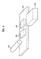
- FIG. 6 is a perspective view of schematically illustrating a printing system according to the fourth embodiment of the present invention.
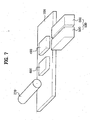
- FIG. 7 is a perspective view of schematically illustrating a printing system according to the fifth embodiment of the present invention.
- FIG. 8 is a perspective view of schematically illustrating a printing system according to the sixth embodiment of the present invention.
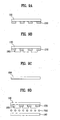
- FIGs. 9A to 9D are cross sectional views of schematically illustrating a method for manufacturing an LCD device according to the preferred embodiment of the present invention.
- FIG. 2A to 2C are cross sectional views of illustrating a process for patterning a pattern material on a substrate using a printing roller and a cliché plate according to the present invention.
- a pattern material 200 is supplied through a printing nozzle 250 and is coated on an outer circumferential surface of a printing roller 270.
- the printing roller 270 coated with the pattern material 200 is rolled on a cliché plate 600 having a plurality of predetermined projections 650, some pattern material 200b is transcribed to the projections 650 of the cliché plate 600.
- the remaining pattern material 200a is left on the outer circumferential surface of the printing roller 270, whereby the pattern material 200a which is left on the outer circumferential surface of the printing roller 270 is formed in a predetermined pattern.
- the printing roller 270 on which the pattern material 200a is left in the predetermined pattern, is rolled on a substrate 100. Accordingly, the remaning pattern material 200a of the printing roller 270 is transcribed to the substrate 100.
- the above patterning method using the printing roll and the cliché plate doesn't use a mask of a predetermined pattern. As a result, the above patterning method can decrease manufacturing cost and time since the above patterning method doesn't perform exposure and development.
- a cleaning unit for cleaning the cliché plate is positioned inside the printing system.
- the pattern material 200b is left on the projections 650 of the cliché plate.
- the cleaning unit for cleaning the cliché plate may include a cleaning part which moves to the cliché plate and cleans the cliché plate.
- the printing system may include the cliché plate, the substrate and cleaning unit sequentially arranged in line, or may include the substrate, the cliché plate and the cleaning unit sequentially arranged in line.
- the cleaning unit may be positioned outside a moving rail.
- the printing system may include the cliché plate and the substrate sequentially and linearly arranged on the moving rail, or may include the substrate and the cliche plate sequentially and linearly arranged on the moving rail.
- the cleaning unit may be positioned at a lateral side of the cliché plate.
- the cleaning part may include a cleaning solution sprayer and a dryer.
- the cleaning unit may include the cleaning part for cleaning the cliché plate, and a container for accommodating a new cliché plate and the cleaned cliché plate.
- the cleaning unit may be positioned outside the moving rail.
- the printing system may include the cliché plate and the substrate sequentially and linearly arranged on the moving rail, or may include the substrate and the cliché plate sequentially and linearly arranged on the moving rail. At this time, the cleaning unit may be positioned at a lateral side of the cliché plate.
- the cleaning part may be comprised of a cleaning solution sprayer and a dryer.
- the cleaning part may include an additional transporter which transports the cliché plate for the cleaning to the cleaning part and transports the cleaned cliché plate from the container to the moving rail.
- a method for manufacturing an LCD device includes steps of forming a light-shielding layer on a first substrate; forming a color filter layer on the first substrate including the light-shielding layer; preparing a second substrate; and forming a liquid crystal layer between the first and second substrates.
- At least any one of the processes of forming the light-shielding layer on the first substrate, and forming the color filter layer on the first substrate including the light-shielding layer is performed with the above-mentioned printing system.
- the process of preparing the second substrate using the above-mentioned printing system may be comprised of steps of forming gate and data lines crossing each other to define a pixel region; forming a thin film transistor adjacent to a crossing area of the gate and data lines; and forming a pixel electrode connected with the thin film transistor.
- the process of forming the liquid crystal layer between the first and second substrates may be comprised of steps of forming a sealant having no inlet to any one of the first and second substrates; dispensing an appropriate amount of liquid crystal to the substrate having the sealant; and bonding the two substrates to each other.
- the process of forming the liquid crystal layer between the first and second substrates may be comprised of steps of forming a sealant having an inlet to any one of the first and second substrates; bonding the two substrates to each other; and injecting liquid crystal to a space between the two substrates through the inlet.
- FIG. 3 is a perspective view of illustrating a printing system according to the first embodiment of the present invention.
- the printing system includes a moving rail 300, a cliché plate 600, a substrate 400, a printing roller 270 and a cleaning part 500.
- the cliché plate 600, the substrate 400 and the cleaning part 500 are positioned on the moving rail 300.
- the printing roller 270 is rolled on the cliché plate 600 and the substrate 400 on the moving rail 300, whereby a pattern material of the printing roller 270 is transcribed to the substrate 400.
- the cleaning part 500 includes a sprayer for spraying a cleaning solution to the cliché plate 600 and a dryer for drying the cliché plate 600.
- the cliché plate 600 When positioning the cliché plate 600, the substrate 400 and the cleaning part 500, they are arranged in an order of the cliché plate 600, the substrate 400 and the cleaning part 500.
- the cleaning part 500 moves to the cliché plate 600 and cleans the cliché plate 600.
- FIG. 4 is a perspective view of illustrating a printing system according to the second embodiment of the present invention.
- the printing system according to the second embodiment of the present invention includes a moving rail 300, a cliché plate 600, a substrate 400, a printing roller 270 and a cleaning part 500.
- the components of the printing system according to the second embodiment of the present invention are similar in structure and are dissimilar in arrangement to those of the printing system according to the first embodiment of the present invention.
- the cliché plate 600, the substrate 400 and the cleaning part 500 when positioning the cliché plate 600, the substrate 400 and the cleaning part 500, they are arranged in an order of the cliché plate 600, the substrate 400 and the cleaning part 500. Meanwhile, in case of the printing system according to the second embodiment of the present invention, they are arranged in an order of the substrate 400, the cliché plate 600 and the cleaning part 500.
- the cleaning part 500 moves to the cliché plate 600, and cleans the cliché plate 600. That is, the cleaning part 500 of the printing system according to the second embodiment of the present invention has a shorter moving distance than the cleaning part 500 of the printing system according to the first embodiment of the present invention.
- FIG. 5 is a perspective view of illustrating a printing system according to the third embodiment of the present invention.
- the printing system according to the third embodiment of the present invention includes a moving rail 300, a cliché plate 600, a substrate 400, a printing roller 270 and a cleaning part 500.
- the components of the printing system according to the third embodiment of the present invention are similar in structure to those of the printing system according to the first embodiment of the present invention.
- the printing system according to the third embodiment of the present invention is different in arrangement of the cleaning part 500 from the printing system according to the first embodiment of the present invention.
- the cleaning part 500 is positioned on the moving rail 300.
- the cleaning part 500 is positioned at a lateral side of the cliché plate 600 outside the moving rail 300.
- the printing system according to the third embodiment of the present invention is identical in operation to the printing system according to the first embodiment of the present invention.
- FIG. 6 is a perspective view of illustrating a printing system according to the fourth embodiment of the present invention.
- the printing system according to the fourth embodiment of the present invention includes a moving rail 300, a cliché plate 600, a substrate 400, a printing roller 270 and a cleaning part 500.
- the components of the printing system according to the fourth embodiment of the present invention are similar in structure and are dissimilar in arrangement to those of the printing system according to the third embodiment of the present invention.
- the cliché plate 600 and the substrate 400 when positioning the cliché plate 600 and the substrate 400, they are arranged in an order of the cliché plate 600 and the substrate 400. However, in the printing system according to the fourth embodiment of the present invention, they are arranged in an order of the substrate 400 and the cliché plate 600.
- the printing system according to the fourth embodiment of the present invention is identical in operation to the printing system according to the second embodiment of the present invention.
- FIG. 7 is a perspective view of illustrating a printing system according to the fifth embodiment of the present invention.
- the printing system according to the fifth embodiment of the present invention includes a moving rail 300, a cliché plate 600, a substrate 400, a printing roller 270 and a cleaning unit 530. Except the cleaning unit 530 of the printing system according to the fifth embodiment of the present invention, the components of the printing system according to the fifth embodiment of the present invention are similar in structure and arrangement to those of the printing system according to the third embodiment of the present invention.
- the cleaning unit 530 is positioned at a lateral side of the cliché plate 600.
- the cleaning unit 530 is comprised of a cleaning part 500 and a container 560.
- the cleaning part 500 cleans the cliché plate 600 by removing the remaining pattern material from the cliché plate 600.
- the container 560 accommodates the unused cliché plate 600 or the cliché plate 600 cleaned in the cleaning part 500. Also, the container 560 transfers the unused cliché plate 600 or the cliché plate 600 cleaned in the cleaning part 500 to the moving rail 300 when the contaminated cliché plate 600 is moved to the cleaning part 500.
- the cleaning unit including both the cleaning part and the container requires a transporter for transporting the cliché plate 600 to the cleaning part 500 and the container 560 since the cleaning part of the cleaning unit is positioned outside the moving rail 300.
- the cliché plate 600 is moved to and cleaned in the cleaning part 500, and the cleaned cliché plate 600 is transferred to the moving rail 300 from the container 560. In this respect, it is possible to treat the plurality of cliché plates with one cleaning part.
- FIG. 8 is a perspective view of illustrating a printing system according to the sixth embodiment of the present invention.
- the printing system according to the sixth embodiment of the present invention includes a moving rail 300, a cliché plate 600, a substrate 400, a printing roller 270 and a cleaning unit 530.
- the components of the printing system according to the sixth embodiment of the present invention are similar in structure and are dissimilar in arrangement to those of the printing system according to the fifth embodiment of the present invention.
- the cliché plate 600 and the substrate 400 when positioning the cliché plate 600 and the substrate 400 on the moving rail 300, they are arranged in an order of the cliché plate 600 and the substrate 400. In the printing system according to the sixth embodiment of the present invention, they are arranged in an order of the substrate 400 and the cliché plate 600.
- FIGs. 9A to 9D are cross sectional views of schematically illustrating a method for manufacturing an LCD device according to the preferred embodiment of the present invention.
- a light-shielding layer 230 is formed on a first substrate 130.
- a color filter layer 260 is formed on the first substrate 130 including the light-shielding layer 230.
- At least any one of the processes for forming the light-shielding layer 230 (FIG. 9A) and forming the color filter layer 260 (FIG. 9B) is performed by the patterning method using the above-mentioned printing system.
- a second substrate 160 is prepared.
- the second substrate 160 is prepared by steps of forming gate and data lines crossing each other to define a unit pixel region on the second substrate; forming a thin film transistor adjacent to a crossing area of the gate and data lines; and forming a pixel electrode connected with the thin film transistor.
- a liquid crystal layer 700 is formed between the first substrate 130 and the second substrate 160.
- the liquid crystal layer 700 may be formed in a liquid crystal injection method or a liquid crystal dispensing method.
- the liquid crystal dispensing method includes steps of forming a sealant having no inlet to any one of the first and second substrates 130 and 160; dispensing liquid crystal to the substrate having the sealant; and bonding the first and second substrates 130 and 160 to each other.
- the liquid crystal injection method includes steps of forming a sealant having an inlet to any one of the first and second substrates 130 and 160; bonding the first and second substrates 130 and 160 to each other; and injecting liquid crystal to an inner space between the first and second substrates 130 and 160 by capillary phenomenon and pressure difference.
- the printing system according to the present invention and the method for manufacturing the LCD device using the same have the following advantages.
- the printing system according to the present invention can decrease the manufacturing cost and time since the printing system according to the present invention doesn't require the relatively high-priced mask and the exposure and development.
- the printing system according to the present invention includes the additional cleaning part. That is, it is possible to simplify the process if using the printing system including the cleaning part therein.
- the cliché plate is moved to and cleaned in the cleaning part, and the cleaned cliché plate is transferred to the moving rail from the container. In this respect, it is possible to treat the plurality of cliché plates with one cleaning part, to thereby decrease the manufacturing cost.
Landscapes
- Physics & Mathematics (AREA)
- Engineering & Computer Science (AREA)
- Nonlinear Science (AREA)
- Manufacturing & Machinery (AREA)
- Optics & Photonics (AREA)
- General Physics & Mathematics (AREA)
- Chemical & Material Sciences (AREA)
- Crystallography & Structural Chemistry (AREA)
- Mathematical Physics (AREA)
- Mechanical Engineering (AREA)
- Liquid Crystal (AREA)
- Optical Filters (AREA)
- Inking, Control Or Cleaning Of Printing Machines (AREA)
- Devices For Indicating Variable Information By Combining Individual Elements (AREA)
- Printing Methods (AREA)
Abstract
Description
- This application claims the benefit of the
Korean Patent Application No. P2005-114167, filed on November 28, 2005 - The present invention relates to a liquid crystal display (LCD) device, and more particularly, to a printing system for forming a pattern of an LCD device.
- Among various ultra-thin flat type display devices, which include a display screen having a thickness of several centimeters, a liquid crystal display (LCD) device can be widely used for notebook computers, monitors, aircraft, and etc. since it has advantages such as low power consumption and portability.
- The LCD device includes lower and upper substrates facing each other at a predetermined interval therebetween, and a liquid crystal layer formed between the lower and upper substrates. Generally, the lower substrate includes a thin film transistor and a pixel electrode. The upper substrate includes a light-shielding layer, a color filter layer and a common electrode.
- As explained above, the LCD device is comprised of various components which are formed by repeated steps. To pattern the components of the LCD device with various shapes, a photolithography process is used necessarily.
- Hereinafter, a patterning method using a photolithography process according to the related art will be explained as follows.
- First, as shown in FIG. 1A, a
pattern material layer 20 is formed on atransparent substrate 10. - After that, as shown in FIG. 1B, after a
mask 23 of a predetermined pattern is positioned above thepattern material layer 20, light emitted from a light source is applied to thetransparent substrate 10. - Then, as shown in FIG. 1C, a
pattern 20a is completed on thetransparent substrate 10 by development. - However, the photolithography process has a disadvantage of high manufacturing cost since the photolithography process uses the mask of the predetermined pattern. In addition, the photolithography process requires the exposure and development.
- To overcome these disadvantages of the photolithography process, it is necessary to develop a new patterning method.
- Accordingly, the present invention is directed to a printing system and a method for manufacturing an LCD device using the printing system, which substantially obviates one or more problems due to limitations and disadvantages of the related art.
- An object of the present invention is to provide a printing system for manufacturing an LCD device with low manufacturing cost and decreased manufacturing time.
- Another object of the present invention is to provide a method for manufacturing an LCD device using the printing system.
- Additional advantages, objects and features of the invention will be set forth in part in the description which follows and in part will become apparent to those having ordinary skill in the art upon examination of the following or may be learned from practice of the invention. The objectives and other advantages of the invention may be realized and attained by the structure particularly pointed out in the written description and claims hereof as well as the appended drawings.
- To achieve these objects and other advantages and in accordance with the purpose of the invention, as embodied and broadly described herein, a printing system comprises a moving rail; a cliché plate and a substrate positioned on the moving rail; a printing roller for transcribing a pattern material on the substrate by passing through the cliché plate ; and a cleaning unit for cleaning the cliché plate.
- It is to be understood that both the foregoing general description and the following detailed description of the present invention are exemplary and explanatory and are intended to provide further explanation of the invention as claimed.
- The accompanying drawings, which are included to provide a further understanding of the invention and are incorporated in and constitute a part of this application, illustrate embodiment(s) of the invention and together with the description serve to explain the principle of the invention. In the drawings:
- FIGs. 1A to 1C are cross sectional views of schematically illustrating a photolithography process according to the related art;
- FIG. 2A to 2C are cross sectional views of illustrating a process for patterning a pattern material on a substrate using a printing roller according to the present invention;
- FIG. 3 is a perspective view of schematically illustrating a printing system according to the first embodiment of the present invention;
- FIG. 4 is a perspective view of schematically illustrating a printing system according to the second embodiment of the present invention;
- FIG. 5 is a perspective view of schematically illustrating a printing system according to the third embodiment of the present invention;
- FIG. 6 is a perspective view of schematically illustrating a printing system according to the fourth embodiment of the present invention;
- FIG. 7 is a perspective view of schematically illustrating a printing system according to the fifth embodiment of the present invention;
- FIG. 8 is a perspective view of schematically illustrating a printing system according to the sixth embodiment of the present invention; and
- FIGs. 9A to 9D are cross sectional views of schematically illustrating a method for manufacturing an LCD device according to the preferred embodiment of the present invention.
- Reference will now be made in detail to the preferred embodiments of the present invention, examples of which are illustrated in the accompanying drawings. Wherever possible, the same reference numbers will be used throughout the drawings to refer to the same or like parts.
- Hereinafter, a printing system according to the present invention and a method for manufacturing an LCD device using the printing system will be explained with reference to the accompanying drawings.
- FIG. 2A to 2C are cross sectional views of illustrating a process for patterning a pattern material on a substrate using a printing roller and a cliché plate according to the present invention.
- First, as shown in FIG. 2A, a
pattern material 200 is supplied through aprinting nozzle 250 and is coated on an outer circumferential surface of aprinting roller 270. - As shown in FIG. 2B, according as the
printing roller 270 coated with thepattern material 200 is rolled on acliché plate 600 having a plurality ofpredetermined projections 650, somepattern material 200b is transcribed to theprojections 650 of thecliché plate 600. The remainingpattern material 200a is left on the outer circumferential surface of theprinting roller 270, whereby thepattern material 200a which is left on the outer circumferential surface of theprinting roller 270 is formed in a predetermined pattern. - As shown in FIG. 2C, the
printing roller 270, on which thepattern material 200a is left in the predetermined pattern, is rolled on asubstrate 100. Accordingly, theremaning pattern material 200a of theprinting roller 270 is transcribed to thesubstrate 100. - The above patterning method using the printing roll and the cliché plate doesn't use a mask of a predetermined pattern. As a result, the above patterning method can decrease manufacturing cost and time since the above patterning method doesn't perform exposure and development.
- Also, a cleaning unit for cleaning the cliché plate is positioned inside the printing system.
- As shown in FIG. 2B, after using the cliché plate, the
pattern material 200b is left on theprojections 650 of the cliché plate. To reuse the cliché plate, it is necessary to perform a cleaning process for the cliché plate. - As the cleaning unit for cleaning the cliché plate is provided inside the printing system, it is possible to decrease the manufacturing time. The cleaning unit may include a cleaning part which moves to the cliché plate and cleans the cliché plate. At this time, the printing system may include the cliché plate, the substrate and cleaning unit sequentially arranged in line, or may include the substrate, the cliché plate and the cleaning unit sequentially arranged in line.
- The cleaning unit may be positioned outside a moving rail. Also, the printing system may include the cliché plate and the substrate sequentially and linearly arranged on the moving rail, or may include the substrate and the cliche plate sequentially and linearly arranged on the moving rail. The cleaning unit may be positioned at a lateral side of the cliché plate.
- Also, the cleaning part may include a cleaning solution sprayer and a dryer. The cleaning unit may include the cleaning part for cleaning the cliché plate, and a container for accommodating a new cliché plate and the cleaned cliché plate.
- The cleaning unit may be positioned outside the moving rail. Also, the printing system may include the cliché plate and the substrate sequentially and linearly arranged on the moving rail, or may include the substrate and the cliché plate sequentially and linearly arranged on the moving rail. At this time, the cleaning unit may be positioned at a lateral side of the cliché plate.
- The cleaning part may be comprised of a cleaning solution sprayer and a dryer. In addition, the cleaning part may include an additional transporter which transports the cliché plate for the cleaning to the cleaning part and transports the cleaned cliché plate from the container to the moving rail.
- If using the cleaning unit including the cleaning part and the container, it is necessary to provide the additional transporter for transporting the cliché plate to the cleaning part.
- In another aspect, a method for manufacturing an LCD device according to the present invention includes steps of forming a light-shielding layer on a first substrate; forming a color filter layer on the first substrate including the light-shielding layer; preparing a second substrate; and forming a liquid crystal layer between the first and second substrates.
- At least any one of the processes of forming the light-shielding layer on the first substrate, and forming the color filter layer on the first substrate including the light-shielding layer is performed with the above-mentioned printing system.
- The process of preparing the second substrate using the above-mentioned printing system may be comprised of steps of forming gate and data lines crossing each other to define a pixel region; forming a thin film transistor adjacent to a crossing area of the gate and data lines; and forming a pixel electrode connected with the thin film transistor.
- The process of forming the liquid crystal layer between the first and second substrates may be comprised of steps of forming a sealant having no inlet to any one of the first and second substrates; dispensing an appropriate amount of liquid crystal to the substrate having the sealant; and bonding the two substrates to each other.
- The process of forming the liquid crystal layer between the first and second substrates may be comprised of steps of forming a sealant having an inlet to any one of the first and second substrates; bonding the two substrates to each other; and injecting liquid crystal to a space between the two substrates through the inlet.
- Hereinafter, a printing system according to the present invention will be described with reference to the accompanying drawings.
- FIG. 3 is a perspective view of illustrating a printing system according to the first embodiment of the present invention.
- As shown in FIG. 3, the printing system according to the first embodiment of the present invention includes a moving
rail 300, acliché plate 600, asubstrate 400, aprinting roller 270 and acleaning part 500. In this case, thecliché plate 600, thesubstrate 400 and thecleaning part 500 are positioned on the movingrail 300. Theprinting roller 270 is rolled on thecliché plate 600 and thesubstrate 400 on the movingrail 300, whereby a pattern material of theprinting roller 270 is transcribed to thesubstrate 400. - The
cleaning part 500 includes a sprayer for spraying a cleaning solution to thecliché plate 600 and a dryer for drying thecliché plate 600. - When positioning the
cliché plate 600, thesubstrate 400 and thecleaning part 500, they are arranged in an order of thecliché plate 600, thesubstrate 400 and thecleaning part 500. - In the printing system according to the first embodiment of the present invention, when the
printing roller 270 coated with the pattern material moves to thecliché plate 600 and thesubstrate 400, and returns to an origin position, thecleaning part 500 moves to thecliché plate 600 and cleans thecliché plate 600. - FIG. 4 is a perspective view of illustrating a printing system according to the second embodiment of the present invention.
- As shown in FIG. 4, the printing system according to the second embodiment of the present invention includes a moving
rail 300, acliché plate 600, asubstrate 400, aprinting roller 270 and acleaning part 500. In this case, the components of the printing system according to the second embodiment of the present invention are similar in structure and are dissimilar in arrangement to those of the printing system according to the first embodiment of the present invention. - In case of the printing system according to the first embodiment of the present invention, when positioning the
cliché plate 600, thesubstrate 400 and thecleaning part 500, they are arranged in an order of thecliché plate 600, thesubstrate 400 and thecleaning part 500. Meanwhile, in case of the printing system according to the second embodiment of the present invention, they are arranged in an order of thesubstrate 400, thecliché plate 600 and thecleaning part 500. - In the printing system according to the second embodiment of the present invention, as the
printing roller 270 coated with a pattern material moves to thecliché plate 600 and returns to an origin position, the pattern material of theprinting roller 270 is transcribed to thecliché plate 600 and thesubstrate 400 in sequence. After transcribing the pattern material to thecliché plate 600, thecleaning part 500 moves to thecliché plate 600, and cleans thecliché plate 600. That is, thecleaning part 500 of the printing system according to the second embodiment of the present invention has a shorter moving distance than the cleaningpart 500 of the printing system according to the first embodiment of the present invention. - FIG. 5 is a perspective view of illustrating a printing system according to the third embodiment of the present invention.
- As shown in FIG. 5, the printing system according to the third embodiment of the present invention includes a moving
rail 300, acliché plate 600, asubstrate 400, aprinting roller 270 and acleaning part 500. In this case, the components of the printing system according to the third embodiment of the present invention are similar in structure to those of the printing system according to the first embodiment of the present invention. However, the printing system according to the third embodiment of the present invention is different in arrangement of thecleaning part 500 from the printing system according to the first embodiment of the present invention. - In the printing system according to the first embodiment of the present invention, the
cleaning part 500 is positioned on the movingrail 300. In the printing system according to the third embodiment of the present invention, thecleaning part 500 is positioned at a lateral side of thecliché plate 600 outside the movingrail 300. - The printing system according to the third embodiment of the present invention is identical in operation to the printing system according to the first embodiment of the present invention.
- FIG. 6 is a perspective view of illustrating a printing system according to the fourth embodiment of the present invention.
- As shown in FIG. 6, the printing system according to the fourth embodiment of the present invention includes a moving
rail 300, acliché plate 600, asubstrate 400, aprinting roller 270 and acleaning part 500. In this case, the components of the printing system according to the fourth embodiment of the present invention are similar in structure and are dissimilar in arrangement to those of the printing system according to the third embodiment of the present invention. - In the printing system according to the third embodiment of the present invention, when positioning the
cliché plate 600 and thesubstrate 400, they are arranged in an order of thecliché plate 600 and thesubstrate 400. However, in the printing system according to the fourth embodiment of the present invention, they are arranged in an order of thesubstrate 400 and thecliché plate 600. - The printing system according to the fourth embodiment of the present invention is identical in operation to the printing system according to the second embodiment of the present invention.
- FIG. 7 is a perspective view of illustrating a printing system according to the fifth embodiment of the present invention.
- As shown in FIG. 7, the printing system according to the fifth embodiment of the present invention includes a moving
rail 300, acliché plate 600, asubstrate 400, aprinting roller 270 and acleaning unit 530. Except thecleaning unit 530 of the printing system according to the fifth embodiment of the present invention, the components of the printing system according to the fifth embodiment of the present invention are similar in structure and arrangement to those of the printing system according to the third embodiment of the present invention. - The
cleaning unit 530 is positioned at a lateral side of thecliché plate 600. Thecleaning unit 530 is comprised of acleaning part 500 and acontainer 560. - After the
cliché plate 600 contaminated due to a pattern material is moved to thecleaning part 500 through the movingrail 300, thecleaning part 500 cleans thecliché plate 600 by removing the remaining pattern material from thecliché plate 600. Thecontainer 560 accommodates theunused cliché plate 600 or thecliché plate 600 cleaned in thecleaning part 500. Also, thecontainer 560 transfers theunused cliché plate 600 or thecliché plate 600 cleaned in thecleaning part 500 to the movingrail 300 when the contaminatedcliché plate 600 is moved to thecleaning part 500. - Unlike the case of using only cleaning part, the cleaning unit including both the cleaning part and the container requires a transporter for transporting the
cliché plate 600 to thecleaning part 500 and thecontainer 560 since the cleaning part of the cleaning unit is positioned outside the movingrail 300. - If using the
cleaning unit 530 in the printing system, thecliché plate 600 is moved to and cleaned in thecleaning part 500, and the cleanedcliché plate 600 is transferred to the movingrail 300 from thecontainer 560. In this respect, it is possible to treat the plurality of cliché plates with one cleaning part. - FIG. 8 is a perspective view of illustrating a printing system according to the sixth embodiment of the present invention.
- As shown in FIG. 8, the printing system according to the sixth embodiment of the present invention includes a moving
rail 300, acliché plate 600, asubstrate 400, aprinting roller 270 and acleaning unit 530. In this case, the components of the printing system according to the sixth embodiment of the present invention are similar in structure and are dissimilar in arrangement to those of the printing system according to the fifth embodiment of the present invention. - In the printing system according to the fifth embodiment of the present invention, when positioning the
cliché plate 600 and thesubstrate 400 on the movingrail 300, they are arranged in an order of thecliché plate 600 and thesubstrate 400. In the printing system according to the sixth embodiment of the present invention, they are arranged in an order of thesubstrate 400 and thecliché plate 600. - Hereinafter, a method for manufacturing an LCD device according to the present invention will be described with reference to the accompanying drawings.
- FIGs. 9A to 9D are cross sectional views of schematically illustrating a method for manufacturing an LCD device according to the preferred embodiment of the present invention.
- First, as shown in FIG. 9A, a light-
shielding layer 230 is formed on afirst substrate 130. Then, as shown in FIG. 9B, acolor filter layer 260 is formed on thefirst substrate 130 including the light-shielding layer 230. - At least any one of the processes for forming the light-shielding layer 230 (FIG. 9A) and forming the color filter layer 260 (FIG. 9B) is performed by the patterning method using the above-mentioned printing system.
- Then, as shown in FIG. 9C, a
second substrate 160 is prepared. Although not shown, thesecond substrate 160 is prepared by steps of forming gate and data lines crossing each other to define a unit pixel region on the second substrate; forming a thin film transistor adjacent to a crossing area of the gate and data lines; and forming a pixel electrode connected with the thin film transistor. - After that, as shown in FIG. 9D, a
liquid crystal layer 700 is formed between thefirst substrate 130 and thesecond substrate 160. - At this time, the
liquid crystal layer 700 may be formed in a liquid crystal injection method or a liquid crystal dispensing method. - The liquid crystal dispensing method includes steps of forming a sealant having no inlet to any one of the first and
second substrates second substrates - The liquid crystal injection method includes steps of forming a sealant having an inlet to any one of the first and
second substrates second substrates second substrates - As mentioned above, the printing system according to the present invention and the method for manufacturing the LCD device using the same have the following advantages.
- The printing system according to the present invention can decrease the manufacturing cost and time since the printing system according to the present invention doesn't require the relatively high-priced mask and the exposure and development.
- Also, the printing system according to the present invention includes the additional cleaning part. That is, it is possible to simplify the process if using the printing system including the cleaning part therein.
- If using the cleaning unit including the cleaning part and the container, the cliché plate is moved to and cleaned in the cleaning part, and the cleaned cliché plate is transferred to the moving rail from the container. In this respect, it is possible to treat the plurality of cliché plates with one cleaning part, to thereby decrease the manufacturing cost.
- It will be apparent to those skilled in the art that various modifications and variations can be made in the present invention without departing from the spirit or scope of the inventions. Thus, it is intended that the present invention covers the modifications and variations of this invention provided they come within the scope of the appended claims and their equivalents.
Claims (20)
- A printing system comprising:a moving rail;a cliché plate and a substrate positioned on the moving rail;a printing roller for transcribing a pattern material on the substrate by passing through the cliché plate; anda cleaning unit for cleaning the cliché plate.
- The printing system of claim 1, wherein the cleaning unit includes a cleaning part for moving and cleaning the cliché plate.
- The printing system of claim 2, wherein the cliché plate, the substrate and the cleaning unit are sequentially arranged in line.
- The printing system of claim 2, wherein the substrate, the cliché plate and the cleaning unit are sequentially arranged in line.
- The printing system of claim 2, wherein the cleaning part is provided outside the moving rail.
- The printing system of claim 5, wherein the cliché plate and the substrate are sequentially arranged in line.
- The printing system of claim 5, wherein the substrate and the cliché plate are sequentially arranged in line.
- The printing system of claim 5, wherein the cleaning part is positioned at a lateral side of the cliché plate outside the moving rail.
- The printing system of claim 2, wherein the cleaning part includes a cleaning solution sprayer and a dryer.
- The printing system of claim 1, wherein the cleaning unit includes a cleaning part for cleaning the cliché plate, and a container for accommodating a new cliché plate and the cleaned cliché plate.
- The printing system of claim 10, wherein the cleaning unit is positioned outside the moving rail.
- The printing system of claim 11, wherein the cliché plate and the substrate are sequentially arranged in line.
- The printing system of claim 11, wherein the substrate and the cliché plate are sequentially arranged in line.
- The printing system of claim 11, wherein the cleaning unit is positioned at a lateral side of the cliché plate outside the moving rail.
- The printing system of claim 10, wherein the cleaning unit includes a cleaning solution sprayer and a dryer.
- The printing system of claim 10, wherein the cleaning unit includes a transporter for transporting the cliché plate.
- A method for manufacturing an LCD device comprising:forming a light-shielding layer on a first substrate;forming a color filter layer on the first substrate including the light-shielding layer;preparing a second substrate; andforming a liquid crystal layer between the first and second substrates,wherein at least any one of the processes of forming the light-shielding layer on the first substrate, and forming the color filter layer on the first substrate including the light-shielding layer is performed with the printing system explained in any one of claims 1 to 16.
- The method of claim 17, wherein the process of preparing the second substrate includes steps of:forming gate and data lines crossing each other on the second substrate, to define pixel regions;forming a thin film transistor adjacent to a crossing area of the gate and data lines;forming a passivation layer on the first substrate including the thin film transistor; andforming a pixel electrode on the passivation layer, the pixel electrode connected with a drain electrode of the thin film transistor, andthe process of the preparing the second substrate is performed with the printing system explained in any one of claims 1 to 16.
- The method of claim 17, wherein the process of forming the liquid crystal layer between the first and second substrates includes steps of:forming a sealant having no inlet to any one of the first and second substrates;dispensing an appropriate amount of liquid crystal to the substrate having the sealant; andbonding the two substrates to each other.
- The method of claim 17, wherein the process of forming the liquid crystal layer between the first and second substrates includes steps of:forming a sealant having an inlet to any one of the first and second substrates;bonding the two substrates to each other; andinjecting liquid crystal to a space between the first and second substrates.
Applications Claiming Priority (1)
| Application Number | Priority Date | Filing Date | Title |
|---|---|---|---|
| KR1020050114167A KR101157967B1 (en) | 2005-11-28 | 2005-11-28 | Printing system and Method of manufacturing of Liquid Crystal Display Device using the same |
Publications (2)
| Publication Number | Publication Date |
|---|---|
| EP1791018A1 true EP1791018A1 (en) | 2007-05-30 |
| EP1791018B1 EP1791018B1 (en) | 2009-08-19 |
Family
ID=37771003
Family Applications (1)
| Application Number | Title | Priority Date | Filing Date |
|---|---|---|---|
| EP06116151A Ceased EP1791018B1 (en) | 2005-11-28 | 2006-06-27 | Printing system and method for manufacturing a liquid crystal display device using the same |
Country Status (7)
| Country | Link |
|---|---|
| US (2) | US7658147B2 (en) |
| EP (1) | EP1791018B1 (en) |
| JP (1) | JP4567633B2 (en) |
| KR (1) | KR101157967B1 (en) |
| CN (1) | CN100592158C (en) |
| DE (1) | DE602006008556D1 (en) |
| TW (1) | TWI317697B (en) |
Families Citing this family (11)
| Publication number | Priority date | Publication date | Assignee | Title |
|---|---|---|---|---|
| KR101255294B1 (en) * | 2005-12-29 | 2013-04-23 | 엘지디스플레이 주식회사 | Printing Apparatus and Method of manufacturing Liquid Crystal Display Device using the same |
| KR101308458B1 (en) * | 2007-03-30 | 2013-09-16 | 엘지디스플레이 주식회사 | Printing device and method for forming pattern using the same |
| JP2010284828A (en) | 2009-06-09 | 2010-12-24 | Ihi Corp | Offset printer |
| KR101419573B1 (en) * | 2010-11-22 | 2014-07-15 | 한국전자통신연구원 | offset printer and printing method of the same |
| US20130142947A1 (en) * | 2011-12-02 | 2013-06-06 | Jo Shan Wu | Method and Device for Manufacturing Color Filter |
| CN102566134A (en) * | 2011-12-02 | 2012-07-11 | 深圳市华星光电技术有限公司 | Method for manufacturing substrate with colored film and manufacturing device |
| KR20130101328A (en) | 2012-03-05 | 2013-09-13 | 삼성전자주식회사 | Cleaning apparatus for printing plate and printing apparatus including the same |
| KR101496957B1 (en) * | 2013-01-14 | 2015-03-02 | (주)피엔티 | Apparatus for dealing with surface |
| CN103522750B (en) * | 2013-10-11 | 2016-01-20 | 南京中电熊猫液晶显示科技有限公司 | Liquid crystal display printing equipment |
| JP2015159277A (en) * | 2014-01-23 | 2015-09-03 | パナソニック株式会社 | Manufacturing method of electronic device |
| CN108906735A (en) * | 2018-07-25 | 2018-11-30 | 武汉华星光电技术有限公司 | A kind of transfer plate cleaning device |
Citations (6)
| Publication number | Priority date | Publication date | Assignee | Title |
|---|---|---|---|---|
| WO1990005065A1 (en) | 1988-11-05 | 1990-05-17 | Basf Aktiengesellschaft | Device for cleaning photopolymer printing plates with solvents, drying said printing plates and recovering the solvents |
| WO1993019483A1 (en) | 1992-03-23 | 1993-09-30 | Brody Thomas P | Process for fabricating an active matrix circuit |
| US5335595A (en) | 1992-07-01 | 1994-08-09 | Nsk Ltd. | Roller offset printing apparatus |
| JPH11254655A (en) | 1998-03-05 | 1999-09-21 | Rohm Co Ltd | Method and device for cleaning screen printing plate |
| US20030081095A1 (en) * | 2001-10-30 | 2003-05-01 | Lg.Philips Lcd Co., Ltd. | Printing system and method for fabricating a liquid crystal display device |
| US20040123753A1 (en) | 2002-12-27 | 2004-07-01 | Lg. Philips Lcd Co., Ltd. | Method of fabricating color filter in display device |
Family Cites Families (11)
| Publication number | Priority date | Publication date | Assignee | Title |
|---|---|---|---|---|
| JP2536956B2 (en) * | 1990-02-28 | 1996-09-25 | 東伸工業株式会社 | Screen changing device for automatic screen printing machine |
| US5367953A (en) * | 1992-07-01 | 1994-11-29 | Nsk Ltd. | Roller offset printing apparatus |
| US5533447A (en) * | 1993-11-03 | 1996-07-09 | Corning Incorporated | Method and apparatus for printing a color filter ink pattern |
| JP3689536B2 (en) * | 1997-08-12 | 2005-08-31 | 光村印刷株式会社 | Image forming method |
| KR20030033874A (en) * | 2001-10-25 | 2003-05-01 | 엘지.필립스 엘시디 주식회사 | Apparatus For Printing An Alignment Layer And The Printing Method Using The Same |
| US6732643B2 (en) * | 2001-11-07 | 2004-05-11 | Lg. Philips Lcd Co., Ltd. | Method for forming pattern using printing process |
| KR100909422B1 (en) * | 2002-12-31 | 2009-07-24 | 엘지디스플레이 주식회사 | Pattern of Liquid Crystal Display and Formation Method |
| JP4108012B2 (en) * | 2003-07-08 | 2008-06-25 | 光村印刷株式会社 | Resin coated substrate manufacturing equipment |
| JP4419477B2 (en) * | 2003-08-27 | 2010-02-24 | 凸版印刷株式会社 | Printing pattern transfer method, liquid crystal display color filter manufacturing method and manufacturing apparatus |
| JP4094539B2 (en) * | 2003-12-12 | 2008-06-04 | 株式会社半導体エネルギー研究所 | Method for manufacturing semiconductor integrated circuit |
| JP2005310400A (en) * | 2004-04-16 | 2005-11-04 | Toppan Printing Co Ltd | Method for producing polymer electroluminescence device |
-
2005
- 2005-11-28 KR KR1020050114167A patent/KR101157967B1/en not_active Expired - Fee Related
-
2006
- 2006-06-22 JP JP2006172219A patent/JP4567633B2/en not_active Expired - Fee Related
- 2006-06-27 EP EP06116151A patent/EP1791018B1/en not_active Ceased
- 2006-06-27 DE DE602006008556T patent/DE602006008556D1/en active Active
- 2006-06-29 US US11/479,135 patent/US7658147B2/en active Active
- 2006-06-30 TW TW095124068A patent/TWI317697B/en not_active IP Right Cessation
- 2006-06-30 CN CN200610100597A patent/CN100592158C/en not_active Expired - Fee Related
-
2009
- 2009-12-17 US US12/641,048 patent/US20100095860A1/en not_active Abandoned
Patent Citations (6)
| Publication number | Priority date | Publication date | Assignee | Title |
|---|---|---|---|---|
| WO1990005065A1 (en) | 1988-11-05 | 1990-05-17 | Basf Aktiengesellschaft | Device for cleaning photopolymer printing plates with solvents, drying said printing plates and recovering the solvents |
| WO1993019483A1 (en) | 1992-03-23 | 1993-09-30 | Brody Thomas P | Process for fabricating an active matrix circuit |
| US5335595A (en) | 1992-07-01 | 1994-08-09 | Nsk Ltd. | Roller offset printing apparatus |
| JPH11254655A (en) | 1998-03-05 | 1999-09-21 | Rohm Co Ltd | Method and device for cleaning screen printing plate |
| US20030081095A1 (en) * | 2001-10-30 | 2003-05-01 | Lg.Philips Lcd Co., Ltd. | Printing system and method for fabricating a liquid crystal display device |
| US20040123753A1 (en) | 2002-12-27 | 2004-07-01 | Lg. Philips Lcd Co., Ltd. | Method of fabricating color filter in display device |
Also Published As
| Publication number | Publication date |
|---|---|
| JP2007144984A (en) | 2007-06-14 |
| EP1791018B1 (en) | 2009-08-19 |
| US7658147B2 (en) | 2010-02-09 |
| US20070119322A1 (en) | 2007-05-31 |
| US20100095860A1 (en) | 2010-04-22 |
| KR101157967B1 (en) | 2012-06-25 |
| TWI317697B (en) | 2009-12-01 |
| KR20070055774A (en) | 2007-05-31 |
| CN100592158C (en) | 2010-02-24 |
| DE602006008556D1 (en) | 2009-10-01 |
| JP4567633B2 (en) | 2010-10-20 |
| CN1975525A (en) | 2007-06-06 |
| TW200720093A (en) | 2007-06-01 |
Similar Documents
| Publication | Publication Date | Title |
|---|---|---|
| US20100095860A1 (en) | Printing system and method for manufacturing liquid crystal display device using the same | |
| US7987782B2 (en) | Printing apparatus for liquid crystal display device and pattern forming method using the same | |
| US20080000374A1 (en) | Printing apparatus, patterning method, and method of fabricating liquid crystal display device using the same | |
| US20090223396A1 (en) | Printing device system and patterning method using the same | |
| US8893618B2 (en) | Patterning method and method for manufacturing liquid crystal display device using the same | |
| US7528927B2 (en) | Fabrication method of liquid crystal display panel and seal pattern forming device using the same | |
| US7276445B2 (en) | Method for forming pattern using printing method | |
| CN101100145B (en) | Printing device system, patterning method using the same, and method of fabricating liquid crystal display device using the same | |
| US7430962B2 (en) | Printing device and printing method using the same | |
| US7441502B2 (en) | Printing apparatus and method for forming patterns for liquid crystal display device using the same | |
| US20070084367A1 (en) | Printing device system and patterning method using the same | |
| US7830491B2 (en) | Sealant dispensing apparatus and method for manufacturing liquid crystal display device using the same |
Legal Events
| Date | Code | Title | Description |
|---|---|---|---|
| PUAI | Public reference made under article 153(3) epc to a published international application that has entered the european phase |
Free format text: ORIGINAL CODE: 0009012 |
|
| 17P | Request for examination filed |
Effective date: 20060627 |
|
| AK | Designated contracting states |
Kind code of ref document: A1 Designated state(s): AT BE BG CH CY CZ DE DK EE ES FI FR GB GR HU IE IS IT LI LT LU LV MC NL PL PT RO SE SI SK TR |
|
| AX | Request for extension of the european patent |
Extension state: AL BA HR MK YU |
|
| 17Q | First examination report despatched |
Effective date: 20071128 |
|
| AKX | Designation fees paid |
Designated state(s): DE FR GB |
|
| RAP1 | Party data changed (applicant data changed or rights of an application transferred) |
Owner name: LG DISPLAY CO., LTD. |
|
| GRAP | Despatch of communication of intention to grant a patent |
Free format text: ORIGINAL CODE: EPIDOSNIGR1 |
|
| GRAS | Grant fee paid |
Free format text: ORIGINAL CODE: EPIDOSNIGR3 |
|
| GRAA | (expected) grant |
Free format text: ORIGINAL CODE: 0009210 |
|
| AK | Designated contracting states |
Kind code of ref document: B1 Designated state(s): DE FR GB |
|
| REG | Reference to a national code |
Ref country code: GB Ref legal event code: FG4D |
|
| REF | Corresponds to: |
Ref document number: 602006008556 Country of ref document: DE Date of ref document: 20091001 Kind code of ref document: P |
|
| PLBE | No opposition filed within time limit |
Free format text: ORIGINAL CODE: 0009261 |
|
| STAA | Information on the status of an ep patent application or granted ep patent |
Free format text: STATUS: NO OPPOSITION FILED WITHIN TIME LIMIT |
|
| 26N | No opposition filed |
Effective date: 20100520 |
|
| REG | Reference to a national code |
Ref country code: FR Ref legal event code: PLFP Year of fee payment: 11 |
|
| REG | Reference to a national code |
Ref country code: FR Ref legal event code: PLFP Year of fee payment: 12 |
|
| REG | Reference to a national code |
Ref country code: FR Ref legal event code: PLFP Year of fee payment: 13 |
|
| PGFP | Annual fee paid to national office [announced via postgrant information from national office to epo] |
Ref country code: GB Payment date: 20220420 Year of fee payment: 17 Ref country code: FR Payment date: 20220425 Year of fee payment: 17 Ref country code: DE Payment date: 20220420 Year of fee payment: 17 |
|
| REG | Reference to a national code |
Ref country code: DE Ref legal event code: R119 Ref document number: 602006008556 Country of ref document: DE |
|
| GBPC | Gb: european patent ceased through non-payment of renewal fee |
Effective date: 20230627 |
|
| PG25 | Lapsed in a contracting state [announced via postgrant information from national office to epo] |
Ref country code: DE Free format text: LAPSE BECAUSE OF NON-PAYMENT OF DUE FEES Effective date: 20240103 Ref country code: GB Free format text: LAPSE BECAUSE OF NON-PAYMENT OF DUE FEES Effective date: 20230627 |
|
| PG25 | Lapsed in a contracting state [announced via postgrant information from national office to epo] |
Ref country code: FR Free format text: LAPSE BECAUSE OF NON-PAYMENT OF DUE FEES Effective date: 20230630 |