EP1785980A2 - Pixel and organic light emitting display device using the same - Google Patents
Pixel and organic light emitting display device using the same Download PDFInfo
- Publication number
- EP1785980A2 EP1785980A2 EP06255765A EP06255765A EP1785980A2 EP 1785980 A2 EP1785980 A2 EP 1785980A2 EP 06255765 A EP06255765 A EP 06255765A EP 06255765 A EP06255765 A EP 06255765A EP 1785980 A2 EP1785980 A2 EP 1785980A2
- Authority
- EP
- European Patent Office
- Prior art keywords
- transistor
- voltage
- scan
- terminal
- data
- Prior art date
- Legal status (The legal status is an assumption and is not a legal conclusion. Google has not performed a legal analysis and makes no representation as to the accuracy of the status listed.)
- Granted
Links
Images



Classifications
-
- G—PHYSICS
- G09—EDUCATION; CRYPTOGRAPHY; DISPLAY; ADVERTISING; SEALS
- G09G—ARRANGEMENTS OR CIRCUITS FOR CONTROL OF INDICATING DEVICES USING STATIC MEANS TO PRESENT VARIABLE INFORMATION
- G09G3/00—Control arrangements or circuits, of interest only in connection with visual indicators other than cathode-ray tubes
- G09G3/20—Control arrangements or circuits, of interest only in connection with visual indicators other than cathode-ray tubes for presentation of an assembly of a number of characters, e.g. a page, by composing the assembly by combination of individual elements arranged in a matrix no fixed position being assigned to or needed to be assigned to the individual characters or partial characters
- G09G3/22—Control arrangements or circuits, of interest only in connection with visual indicators other than cathode-ray tubes for presentation of an assembly of a number of characters, e.g. a page, by composing the assembly by combination of individual elements arranged in a matrix no fixed position being assigned to or needed to be assigned to the individual characters or partial characters using controlled light sources
- G09G3/30—Control arrangements or circuits, of interest only in connection with visual indicators other than cathode-ray tubes for presentation of an assembly of a number of characters, e.g. a page, by composing the assembly by combination of individual elements arranged in a matrix no fixed position being assigned to or needed to be assigned to the individual characters or partial characters using controlled light sources using electroluminescent panels
-
- G—PHYSICS
- G09—EDUCATION; CRYPTOGRAPHY; DISPLAY; ADVERTISING; SEALS
- G09G—ARRANGEMENTS OR CIRCUITS FOR CONTROL OF INDICATING DEVICES USING STATIC MEANS TO PRESENT VARIABLE INFORMATION
- G09G3/00—Control arrangements or circuits, of interest only in connection with visual indicators other than cathode-ray tubes
- G09G3/20—Control arrangements or circuits, of interest only in connection with visual indicators other than cathode-ray tubes for presentation of an assembly of a number of characters, e.g. a page, by composing the assembly by combination of individual elements arranged in a matrix no fixed position being assigned to or needed to be assigned to the individual characters or partial characters
- G09G3/22—Control arrangements or circuits, of interest only in connection with visual indicators other than cathode-ray tubes for presentation of an assembly of a number of characters, e.g. a page, by composing the assembly by combination of individual elements arranged in a matrix no fixed position being assigned to or needed to be assigned to the individual characters or partial characters using controlled light sources
- G09G3/30—Control arrangements or circuits, of interest only in connection with visual indicators other than cathode-ray tubes for presentation of an assembly of a number of characters, e.g. a page, by composing the assembly by combination of individual elements arranged in a matrix no fixed position being assigned to or needed to be assigned to the individual characters or partial characters using controlled light sources using electroluminescent panels
- G09G3/32—Control arrangements or circuits, of interest only in connection with visual indicators other than cathode-ray tubes for presentation of an assembly of a number of characters, e.g. a page, by composing the assembly by combination of individual elements arranged in a matrix no fixed position being assigned to or needed to be assigned to the individual characters or partial characters using controlled light sources using electroluminescent panels semiconductive, e.g. using light-emitting diodes [LED]
- G09G3/3208—Control arrangements or circuits, of interest only in connection with visual indicators other than cathode-ray tubes for presentation of an assembly of a number of characters, e.g. a page, by composing the assembly by combination of individual elements arranged in a matrix no fixed position being assigned to or needed to be assigned to the individual characters or partial characters using controlled light sources using electroluminescent panels semiconductive, e.g. using light-emitting diodes [LED] organic, e.g. using organic light-emitting diodes [OLED]
- G09G3/3225—Control arrangements or circuits, of interest only in connection with visual indicators other than cathode-ray tubes for presentation of an assembly of a number of characters, e.g. a page, by composing the assembly by combination of individual elements arranged in a matrix no fixed position being assigned to or needed to be assigned to the individual characters or partial characters using controlled light sources using electroluminescent panels semiconductive, e.g. using light-emitting diodes [LED] organic, e.g. using organic light-emitting diodes [OLED] using an active matrix
- G09G3/3233—Control arrangements or circuits, of interest only in connection with visual indicators other than cathode-ray tubes for presentation of an assembly of a number of characters, e.g. a page, by composing the assembly by combination of individual elements arranged in a matrix no fixed position being assigned to or needed to be assigned to the individual characters or partial characters using controlled light sources using electroluminescent panels semiconductive, e.g. using light-emitting diodes [LED] organic, e.g. using organic light-emitting diodes [OLED] using an active matrix with pixel circuitry controlling the current through the light-emitting element
-
- G—PHYSICS
- G09—EDUCATION; CRYPTOGRAPHY; DISPLAY; ADVERTISING; SEALS
- G09G—ARRANGEMENTS OR CIRCUITS FOR CONTROL OF INDICATING DEVICES USING STATIC MEANS TO PRESENT VARIABLE INFORMATION
- G09G3/00—Control arrangements or circuits, of interest only in connection with visual indicators other than cathode-ray tubes
- G09G3/20—Control arrangements or circuits, of interest only in connection with visual indicators other than cathode-ray tubes for presentation of an assembly of a number of characters, e.g. a page, by composing the assembly by combination of individual elements arranged in a matrix no fixed position being assigned to or needed to be assigned to the individual characters or partial characters
-
- G—PHYSICS
- G09—EDUCATION; CRYPTOGRAPHY; DISPLAY; ADVERTISING; SEALS
- G09G—ARRANGEMENTS OR CIRCUITS FOR CONTROL OF INDICATING DEVICES USING STATIC MEANS TO PRESENT VARIABLE INFORMATION
- G09G2300/00—Aspects of the constitution of display devices
- G09G2300/08—Active matrix structure, i.e. with use of active elements, inclusive of non-linear two terminal elements, in the pixels together with light emitting or modulating elements
- G09G2300/0809—Several active elements per pixel in active matrix panels
- G09G2300/0819—Several active elements per pixel in active matrix panels used for counteracting undesired variations, e.g. feedback or autozeroing
-
- G—PHYSICS
- G09—EDUCATION; CRYPTOGRAPHY; DISPLAY; ADVERTISING; SEALS
- G09G—ARRANGEMENTS OR CIRCUITS FOR CONTROL OF INDICATING DEVICES USING STATIC MEANS TO PRESENT VARIABLE INFORMATION
- G09G2300/00—Aspects of the constitution of display devices
- G09G2300/08—Active matrix structure, i.e. with use of active elements, inclusive of non-linear two terminal elements, in the pixels together with light emitting or modulating elements
- G09G2300/0809—Several active elements per pixel in active matrix panels
- G09G2300/0842—Several active elements per pixel in active matrix panels forming a memory circuit, e.g. a dynamic memory with one capacitor
-
- G—PHYSICS
- G09—EDUCATION; CRYPTOGRAPHY; DISPLAY; ADVERTISING; SEALS
- G09G—ARRANGEMENTS OR CIRCUITS FOR CONTROL OF INDICATING DEVICES USING STATIC MEANS TO PRESENT VARIABLE INFORMATION
- G09G2300/00—Aspects of the constitution of display devices
- G09G2300/08—Active matrix structure, i.e. with use of active elements, inclusive of non-linear two terminal elements, in the pixels together with light emitting or modulating elements
- G09G2300/0809—Several active elements per pixel in active matrix panels
- G09G2300/0842—Several active elements per pixel in active matrix panels forming a memory circuit, e.g. a dynamic memory with one capacitor
- G09G2300/0861—Several active elements per pixel in active matrix panels forming a memory circuit, e.g. a dynamic memory with one capacitor with additional control of the display period without amending the charge stored in a pixel memory, e.g. by means of additional select electrodes
-
- G—PHYSICS
- G09—EDUCATION; CRYPTOGRAPHY; DISPLAY; ADVERTISING; SEALS
- G09G—ARRANGEMENTS OR CIRCUITS FOR CONTROL OF INDICATING DEVICES USING STATIC MEANS TO PRESENT VARIABLE INFORMATION
- G09G2300/00—Aspects of the constitution of display devices
- G09G2300/08—Active matrix structure, i.e. with use of active elements, inclusive of non-linear two terminal elements, in the pixels together with light emitting or modulating elements
- G09G2300/0809—Several active elements per pixel in active matrix panels
- G09G2300/0842—Several active elements per pixel in active matrix panels forming a memory circuit, e.g. a dynamic memory with one capacitor
- G09G2300/0861—Several active elements per pixel in active matrix panels forming a memory circuit, e.g. a dynamic memory with one capacitor with additional control of the display period without amending the charge stored in a pixel memory, e.g. by means of additional select electrodes
- G09G2300/0866—Several active elements per pixel in active matrix panels forming a memory circuit, e.g. a dynamic memory with one capacitor with additional control of the display period without amending the charge stored in a pixel memory, e.g. by means of additional select electrodes by means of changes in the pixel supply voltage
-
- G—PHYSICS
- G09—EDUCATION; CRYPTOGRAPHY; DISPLAY; ADVERTISING; SEALS
- G09G—ARRANGEMENTS OR CIRCUITS FOR CONTROL OF INDICATING DEVICES USING STATIC MEANS TO PRESENT VARIABLE INFORMATION
- G09G2320/00—Control of display operating conditions
- G09G2320/02—Improving the quality of display appearance
- G09G2320/0233—Improving the luminance or brightness uniformity across the screen
-
- G—PHYSICS
- G09—EDUCATION; CRYPTOGRAPHY; DISPLAY; ADVERTISING; SEALS
- G09G—ARRANGEMENTS OR CIRCUITS FOR CONTROL OF INDICATING DEVICES USING STATIC MEANS TO PRESENT VARIABLE INFORMATION
- G09G2320/00—Control of display operating conditions
- G09G2320/04—Maintaining the quality of display appearance
- G09G2320/043—Preventing or counteracting the effects of ageing
Definitions
- the present invention relates to a pixel and an organic light emitting display device using the same, and more particularly, to a pixel for displaying an image with uniform brightness and an organic light emitting display device using the same.
- FIG. 1 is a circuit diagram illustrating a pixel of a conventional organic light emitting display device.
- the pixel 4 of the conventional organic light emitting display device includes a pixel circuit 2 coupled to an organic light emitting diode (OLED), a data line Dm, and a scan line Sn.
- the pixel circuit 2 controls the OLED.
- a first power source ELVDD and a second power source ELVSS are coupled to the pixel 4.
- An anode electrode of the OLED is coupled to the pixel circuit 2 and a cathode electrode of the OLED is coupled to the second power source ELVSS.
- the OLED generates light with brightness corresponding to the current supplied by the pixel circuit 2.
- the pixel circuit 2 controls the amount of current supplied to the OLED in response to a data signal supplied to the data line Dm when a scan signal is supplied to the scan line Sn.
- the pixel circuit 2 includes a first transistor M1, a second transistor M2, and a storage capacitor Cst.
- the second transistor M2 is coupled between the first power source ELVDD and the OLED.
- the first transistor M1 is coupled to the second transistor M2, the data line Dm, and the scan line Sn.
- the storage capacitor Cst is coupled between a gate electrode and a first electrode of the second transistor M2.
- a gate electrode of the first transistor M1 is coupled to the scan line Sn and a first electrode of the first transistor M1 is coupled to the data line Dm.
- a second electrode of the first transistor M1 is coupled to one terminal of the storage capacitor Cst.
- One of the electrodes of each of the first and second transistors M1, M2 is set as a source electrode and the other electrode is set as a drain electrode. For example, when the first electrode is set as the source electrode, the second electrode is set as the drain electrode.
- the first transistor M1 is turned on to supply the data signal supplied by the data line Dm to the storage capacitor Cst. As a result, a voltage corresponding to the data signal is charged in the storage capacitor Cst.
- the gate electrode of the second transistor M2 is coupled to one terminal of the storage capacitor Cst and the first electrode of the second transistor M2 is coupled to the other terminal of the storage capacitor Cst and the first power source ELVDD.
- the second electrode of the second transistor M2 is coupled to the anode electrode of the OLED.
- the second transistor M2 controls the amount of current that flows from the first power source ELVDD to the OLED to correspond to the voltage value stored in the storage capacitor Cst.
- the OLED generates light with the brightness corresponding to the amount of current supplied by the second transistor M2.
- the threshold voltages of the second transistors M2 included in different pixels 4 vary due to deviations introduced during the fabrication processes.
- the threshold voltages of the second transistors M2 are not uniform, although data signals corresponding to the same gray level are supplied to a number of pixels 4, light components with different brightness are generated by the OLEDs of each pixel 4.
- the difference in brightness is due to the difference between the threshold voltages of the second transistors M2 of each pixel.
- embodiments of the present invention provide a pixel for displaying an image with uniform brightness and a light emitting display device using the same.
- an organic light emitting display device as set out in claim 9.
- Preferred features of this aspect are set out in claims 10 to 12.
- FIG. 1 is a schematic circuit diagram illustrating a conventional pixel.
- FIG. 2 schematically illustrates an organic light emitting display device according to a first embodiment of the present invention.
- FIG. 3 is a schematic circuit diagram illustrating a first embodiment of a pixel according to the present invention.
- FIG. 4 schematically illustrates waveforms for describing a method of driving the pixel of FIG. 3.
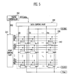
- FIG. 5 schematically illustrates an organic light emitting display device according to a second embodiment of the present invention.
- FIG. 6 is a schematic circuit diagram illustrating a second embodiment of a pixel according to the present invention.
- FIG. 7 schematically illustrates waveforms for describing a method of driving the pixel of FIG. 6.
- FIG. 2 schematically illustrates an organic light emitting display device according to a first embodiment of the present invention.
- the organic light emitting display device includes a scan driving part 110 for driving scan lines S 1 to Sn and emission control lines E1 to En, a data driving part 120 for driving data lines D1 to Dm, a display region 130 including pixels 140 formed in the regions partitioned by the scan lines S1 to Sn and the data lines D1 to Dm, and a timing controller 150 for controlling the scan driving part 110 and the data driving part 120.
- the timing controller 150 receives data Data and synchronizing signals (not shown) from outside of the display device.
- the timing controller 150 generates data driving control signals DCS and scan driving control signals SCS corresponding to the synchronizing signals supplied from outside.
- the data driving control signals DCS generated by the timing controller 150 are supplied to the data driving part 120 and the scan driving control signals SCS generated by the timing controller 150 are supplied to the scan driving part 110.
- the timing controller 150 supplies the data Data supplied from the outside to the data driving part 120.
- the scan driving part 110 receives the scan driving control signals SCS from the timing controller 150.
- the scan driving part 110 that has received the scan driving control signals SCS, generates scan signals to be supplied to the scan lines S 1 to Sn.
- the scan driving part 110 in response to the scan driving control signals SCS, the scan driving part 110 generates emission control signals to be supplied to the emission control lines E1 to En.
- the scan signals may be generated in a sequential manner.
- the width of the emission control signals is equal to or larger than the width of the scan signals.
- the width of a signal may refer to the duration of a pulse of the signal.
- Some signals may have pulses that correspond to a voltage level below a reference level and other signals may have pulses corresponding to a voltage level above the reference level. For example, some signals may have positive pulses and other signals may have negative pulses. If the signals are being applied to gates of transistors for controlling the transistors, then negative pulses turn on PMOS transistors and positive pulses turn on NMOS transistors. Alternatively, if a signal includes positive pulses, then the positive pulses of the signal may be used to turn off a PMOS transistor.
- the data driving part 120 receives the data driving control signals DCS from the timing controller 150.
- the data driving part 120 that has received the data driving control signals DCS generates data signals to be supplied to the data lines D 1 to Dm in synchronization with the scan signals.
- the display region 130 receives power from a first power source ELVDD and a second power source ELVSS and supplies the power to the pixels 140.
- the pixels 140 that have received power from the first power source ELVDD and the second power source ELVSS generate light components corresponding to the data signals.
- the emission times, or duration of emission, of the pixels 140 are controlled by the emission control signals.
- FIG. 3 is a schematic circuit diagram illustrating a first embodiment pixel according to the present invention.
- the first embodiment pixel 140 may be included in the display device of the first embodiment of the present invention that is shown FIG. 2.
- a pixel 140 coupled to an mth data line Dm, an nth scan line Sn, an (n-1)th scan line Sn-1, and an nth emission control line En is illustrated in FIG. 3.
- the pixel 140 includes a pixel circuit 142 that is coupled to the OLED, and also to the data line Dm, the scan lines Sn-1 and Sn, and the emission control line En to control the amount of current supplied to the OLED.
- An anode electrode of the OLED is coupled to the pixel circuit 142 and a cathode electrode of the OLED is coupled to the second power source ELVSS.
- the voltage value of the second power source ELVSS is set to be smaller than the voltage value of the first power source ELVDD.
- the OLED generates light with brightness corresponding to the amount of current supplied by the pixel circuit 142.
- the pixel circuit 142 controls the amount of current supplied to the OLED in response to the data signal supplied to the data line Dm when a scan signal is supplied to the scan line Sn.
- the pixel circuit 142 includes first to sixth transistors M11, M12, M 13, M14, M 15, M16 and a storage capacitor C1st.
- a first electrode of the second transistor M12 is coupled to the data line Dm and a second electrode of the second transistor M12 is coupled to a first node N11.
- a gate electrode of the second transistor M12 is coupled to the nth scan line Sn. When the scan signal is supplied to the nth scan line Sn, the second transistor M12 is turned on to supply the data signal supplied from the data line Dm to the first node N11.
- a first electrode of the first transistor M11 is coupled to the first node N11 and a second electrode of the first transistor M11 is coupled to a first electrode of the sixth transistor M16.
- a gate electrode of the first transistor M11 is coupled to the storage capacitor C1st. The first transistor M11 supplies the current corresponding to the voltage charged in the storage capacitor C1st to the OLED.
- a first electrode of the third transistor M13 is coupled to the second electrode of the first transistor M11 and a second electrode of the third transistor M13 is coupled to the gate electrode of the first transistor M11.
- a gate electrode of the third transistor M13 is coupled to the nth scan line Sn.
- a gate electrode of the fourth transistor M14 is coupled to the (n-1)th scan line Sn-1 and a first electrode of the fourth transistor M14 is coupled to one terminal of the storage capacitor C1st and the gate electrode of the first transistor M11.
- a second electrode of the fourth transistor M14 is coupled to an initialization power source Vint.
- a first electrode of the fifth transistor M15 is coupled to the first power source ELVDD and a second electrode of the fifth transistor M15 is coupled to the first node N11.
- a gate electrode of the fifth transistor M15 is coupled to the emission control line En. When the emission control signal is not being supplied by the emission control line En, the fifth transistor M15 is turned on to electrically connect the first power source ELVDD and the first node N11 to each other.
- the first electrode of the sixth transistor M16 is coupled to the second electrode of the first transistor M11 and a second electrode of the sixth transistor M16 is coupled to the anode electrode of the OLED.
- a gate electrode of the sixth transistor M16 is coupled to the emission control line En. When the emission control signal is not being supplied, the sixth transistor M16 is turned on to supply the current supplied by the first transistor M11 to the OLED.
- FIG. 4 shows the waveforms of the signals applied to the (n-1)th scan line Sn-1, the nth scan line Sn, and the nth emission control line En.
- a scan signal is supplied to the (n-1)th scan line Sn-1 so that the fourth transistor M14 is turned on.
- the fourth transistor M14 is turned on, the voltage of the initialization power source Vint is supplied to one terminal of the storage capacitor C1st and the gate terminal of the first transistor M11, that are both coupled to the first electrode of the fourth transistor M14.
- the voltages of one terminal of the storage capacitor C1st and the gate terminal of the first transistor M11 are initialized to the voltage of the initialization power source Vint.
- the voltage value of the initialization power source Vint is set to be smaller than the voltage value of the data signal.
- the scan signal is supplied to the nth scan line Sn.
- the second and third transistors M12, M13 are turned on.
- the third transistor M13 is turned on, current flows through the first transistor M11 so that the first transistor M11 serves as a diode.
- the second transistor M12 is turned on, the data signal supplied to the data line Dm is supplied to the first node N11 through the second transistor M12.
- the voltage at the gate of the first transistor M11 is initialized to the voltage of the initialization power source Vint and because the voltage of Vint is set to be lower than the voltage of the data signal supplied to the first node N11, the first transistor M11 is turned on.
- the data signal applied to the first node N11 is supplied to the terminal of the storage capacitor C1st, that is coupled to the gate of the first transistor M11, through the first and third transistors M11, M13.
- the data signal is supplied to the storage capacitor C1st through the first transistor M11 which serves as a diode and through which current flows. Therefore, the voltage corresponding to the data signal and a threshold voltage of the first transistor M11 is charged in the storage capacitor C1st.
- the fifth and sixth transistors M15, M16 are turned on.
- the fifth and sixth transistors M15, M16 are turned on, a current path from the first power source ELVDD to the OLED is formed.
- the first transistor M11 controls the amount of current that flows from the first power source ELVDD to the OLED to correspond to the voltage charged in the storage capacitor C1st.
- the voltage corresponding to the data signal and the threshold voltage of the first transistor M11 is charged in the storage capacitor C1st included in the pixel 140.
- the voltages charged in the storage capacitors C1st of different pixels 140 may be different because threshold voltages of the first transistors M11 used in each pixel may be different from one another.
- the threshold voltage is included in the voltage charging the capacitor. As a result, it is possible to control the amount of current that flows to the OLED regardless of the threshold voltage of the first transistor M11. Therefore, various pixels 140 according to the first embodiment of the present invention can display an image with substantially uniform brightness regardless of the threshold voltages of the first transistors M11 used in each of the pixels 140.
- undesired leakage current may originate from the gate terminal of the first transistor M11.
- the fourth transistor M14 when the fourth transistor M14 is off, the voltage of the gate electrode of the first transistor M11 is different from the voltage of the initialization power source Vint.
- the fourth transistor M14 when the voltage of the gate electrode of the first transistor M11 is different from the voltage of the initialization power source Vint, although the fourth transistor M14 is turned off, a leakage current is generated that changes the voltage of the gate electrode of the first transistor M11. That is, in the pixel 140 illustrated in FIG. 3, the voltage of the gate electrode of the first transistor M11 is changed by the leakage current through the fourth transistor M14 so that an image with desired brightness is not displayed.
- FIG. 5 illustrates an organic light emitting display device according to a second embodiment of the present invention.
- the organic light emitting display device includes a scan driving part 210, a data driving part 220, a display region 230, and a timing controller 250.
- the scan driving part 210 drives first scan lines S 11 to S1n, second scan lines S21 to S2n, and emission control lines E1 to En.
- the data driving part 220 drives data lines D1 to Dm.
- the display region 230 includes pixels 240 formed in regions partitioned by the first scan lines S 11 to S1n, the second scan lines S21 to S2n, and the data lines D1 to Dm.
- the timing controller 250 controls the scan driving part 210 and the data driving part 220.
- the timing controller 250 generates data driving control signals DCS and scan driving control signals SCS in response to synchronizing signals supplied from the outside of the display device.
- the data driving control signals DCS generated by the timing controller 250 are supplied to the data driving part 220 and the scan driving control signals SCS generated by the timing controller 250 are supplied to the scan driving part 210.
- the timing controller 250 supplies data Data supplied from the outside to the data driving part 220.
- the scan driving part 210 receives the scan driving control signals SCS from the timing controller 250.
- the scan driving part 210 that has received the scan driving control signals SCS supplies a first scan signal to the first scan lines S11 to S1n and supplies a second scan signal to the second scan lines S21 to S2n.
- the first scan signals may be supplied to the first scan lines S11 to S1n in a sequential manner.
- the second scan signals may be supplied to the second scan lines S21 to S2n in a sequential manner.
- the first and second scan signals supplied to the same pixel 240 are supplied at substantially the same point in time and a width or duration of the first scan signal is set to be larger than a width of the second scan signal. Thus, the first scan signal lasts longer than the second scan signal.
- the scan driving part 210 generates emission control signals in response to the scan driving control signals SCS and supplies the generated emission control signals to the emission control lines E1 to En.
- the emission control signals are supplied to overlap the first scan signals. Further, the width or duration of the emission control signal is set to be larger than the width of the first scan signal.
- the data driving part 220 receives the data driving control signals DCS from the timing controller 250.
- the data driving part 220 that has received the data driving control signals DCS, generates data signals and supplies the generated data signals to the data lines D1 to Dm in synchronization with the first and second scan signals.
- the display region 230 receives power from a first power source ELVDD, a second power source ELVSS and an initialization power source Vint located outside the display region 230.
- the display region 230 supplies the power from the first power source ELVDD, the second power source ELVSS, and the initialization power source Vint to the pixels 240.
- the pixels 240 that have received power from the first power source ELVDD, the second power source ELVSS, and the initialization power source Vint, generate light components corresponding to the data signals.
- the emission times, including the time of commencing the emission and the duration of emission, of the pixels 240 are controlled by the emission control signals.
- FIG. 6 is a circuit diagram illustrating a second embodiment of a pixel 240 according of the present invention.
- the second embodiment pixel 240 may be included in the display device of the second embodiment of the present invention shown in FIG. 5.
- a pixel coupled to an mth data line Dm, an nth first scan line S1n, an nth second scan line S2n, and an nth emission control line En is illustrated in FIG. 6.
- the pixel 240 includes a pixel circuit 242 coupled to an OLED, the data line Dm, the first and second scan lines S1n, S2n, and the emission control line En to control the amount of current supplied to the OLED.
- the anode electrode of the OLED is coupled to the pixel circuit 242 and the cathode electrode of the OLED is coupled to the second power source ELVSS.
- the voltage value of the second power source ELVSS is set to be smaller than the voltage value of the first power source ELVDD.
- the OLED generates light with brightness corresponding to the amount of current supplied by the pixel circuit 242.
- the pixel circuit 242 receives the data signal from the data line Dm when the scan signals are supplied to the first and second scan lines S1n and S2n.
- the pixel circuit 242 controls the amount of current supplied to the OLED in response to the data signal.
- the pixel circuit 242 includes first to sixth transistors M21, M22, M23, M24, M25, M26 and a storage capacitor C2st.
- a first electrode of the second transistor M22 is coupled to the data line Dm and a second electrode of the second transistor M22 is coupled to a first node N21.
- a gate electrode of the second transistor M22 is coupled to the first scan line S1n.
- the second transistor M22 is turned on when the first scan signal is supplied to the first scan line S1n. When turned on, the second transistor M22 supplies the data signal, that is supplied to the data line Dm, to the first node N21.
- a first electrode of the first transistor M21 is coupled to the first power source ELVDD and a second electrode of the first transistor M21 is coupled to a first electrode of the sixth transistor M26.
- a gate electrode of the first transistor M21 is coupled to a second node N22.
- the first transistor M21 supplies the current corresponding to the voltage applied to the second node N22 to the OLED.
- the current supplied by the first transistor M21 to the OLED corresponds to and is controlled by the voltage at the second node N22.
- a first electrode of the third transistor M23 is coupled to the second electrode of the first transistor M21 and a second electrode of the third transistor M23 is coupled to the gate electrode of the first transistor M21.
- a gate electrode of the third transistor M23 is coupled to the first scan line S1n.
- the third transistor M23 is turned on when the first scan signal is supplied to the first scan line S1n.
- the first transistor M21 serves as a diode.
- a first electrode of the fourth transistor M24 is coupled to the second electrode of the first transistor M21 and a second electrode of the fourth transistor M24 is coupled to the initialization power source Vint.
- a gate electrode of the fourth transistor M24 is coupled to the second scan line S2n. The fourth transistor M24 is turned on when the second scan signal is supplied to the second scan line S2n.
- a first electrode of the fifth transistor M25 is coupled to the first node N21 and a second electrode of the fifth transistor M25 is coupled to the initialization power source Vint.
- a gate electrode of the fifth transistor M25 is coupled to the emission control line En.
- the fifth transistor M25 is turned on when the emission control signal is not being supplied by the emission control line En. When turned on, the fifth transistor M25 changes the voltage value of the first node N21 to the voltage value of the initialization power source Vint.
- the first electrode of the sixth transistor M26 is coupled to the second electrode of the first transistor M21 and a second electrode of the sixth transistor M26 is coupled to the anode electrode of the OLED.
- a gate electrode of the sixth transistor M26 is coupled to the emission control line En.
- the sixth transistor M26 is turned on when the emission control signal is not supplied. When turned on, the sixth transistor M26 supplies the current supplied by the first transistor M21 to the OLED.
- the storage capacitor C2st is provided between the first node N21 and the second node N22 to be charged to a voltage established between these two nodes N21, N22.
- Waveforms of FIG. 7 include a second scan signal being applied to the second scan line S2n, a first scan signal being applied to the first scan line S1n, and an emission control signal being applied to the emission control line En.
- the emission control signal is supplied to the emission control line En during a first period T1.
- the fifth and sixth transistors M25, M26 are turned off.
- the transistors are shown as PMOS transistors that are turned on by a negative gate to source voltage and turned off by a positive gate to source voltage.
- the emission control signal being supplied to the emission control line En is shown to be a positive signal. Accordingly, application of the positive signal to the emission control line turns off the PMOS transistors.
- other types of transistors for example NMOS transistors, may be used which are turned on and off by signals different from those shown.
- the second scan signal is supplied only during the period T2.
- the first and second scan signals of the second embodiment coincide partially in time during the period T2.
- the fifth and sixth transistors M25, M26 are turned off, the first scan signal is supplied to the first scan line S1n and, at the same time, the second scan signal is supplied to the second scan line S2n.
- the second and third transistors M22, M23 are turned on.
- the fourth transistor M24 is turned on.
- the second transistor M22 is turned on, the data signal supplied to the data line Dm is supplied to the first node N21.
- the voltage of the initialization power source Vint is supplied to the second node N22.
- the voltage value of the initialization power source Vint is set to be smaller than the voltage value of the data signal.
- a fifth period T5 supply of the emission control signal is stopped. Then, the fifth transistor M25 and the sixth transistor M26 are turned on.
- the fifth transistor M25 is turned on, the voltage value of the first node N21 is reduced to the voltage value of the initialization power source Vint. That is, the voltage value of the first node N21 is reduced from the voltage value of the data signal to the voltage value of the initialization power source Vint.
- the third transistor M23 is off and the second node N22 is floating, the voltage value of the second node N22 is reduced corresponding to the reduction in the voltage value of the first node N21 in order to maintain the same voltage difference between the two nodes N22, N21.
- the voltage value of the second node N22 is also reduced by the voltage value of the data signal from its previous voltage value that was obtained by subtracting the threshold voltage value of the first transistor M21 from the voltage value of the first power source ELVDD.
- the first transistor M21 supplies current corresponding to the value of the voltage applied to the second node N22 to the OLED through the sixth transistor M26 during the fifth period T5 so that light of controlled brightness is generated by the OLED.
- the first to fifth periods, T1, T2, T3, T4, T5 are consecutive in the exemplary embodiment of FIG. 7.
- the voltage value of the second node N22 is initially set as the value obtained by subtracting the threshold voltage value of the first transistor M21 from the voltage value of the first power source ELVDD.
- the voltage value of the second node N22 is subsequently reduced from the initially set voltage value by the voltage value corresponding to the voltage value of the data signal.
- the second node N22 is coupled to the gate of the first transistor M21 and the voltage at the second node N22 determines the amount of current supplied to the OLED by the first transistor M21.
- the fourth transistor M24 that supplies the initialization power source Vint is coupled to the second electrode of the first transistor M21. Therefore, the leakage current through the fourth transistor M24 is from the second electrode of the first transistor M21. As a result, leakage current does not flow from the second node N22 that is the gate electrode of the first transistor M21 to the initialization power source Vint so that it is possible to display an image with desired brightness.
- the amount of current that flows to the OLED is controlled regardless of the threshold voltage of the first transistor. Therefore, it is possible to display an image with uniform brightness.
- the fourth transistor for supplying the initialization power source is coupled to the second electrode of the first transistor, it is possible to reduce or prevent leakage current flowing from the gate electrode of the first transistor so that it is possible to display an image with desired brightness.
Landscapes
- Engineering & Computer Science (AREA)
- Physics & Mathematics (AREA)
- Computer Hardware Design (AREA)
- General Physics & Mathematics (AREA)
- Theoretical Computer Science (AREA)
- Control Of Indicators Other Than Cathode Ray Tubes (AREA)
- Control Of El Displays (AREA)
- Electroluminescent Light Sources (AREA)
Abstract
Description
- The present invention relates to a pixel and an organic light emitting display device using the same, and more particularly, to a pixel for displaying an image with uniform brightness and an organic light emitting display device using the same.
- FIG. 1 is a circuit diagram illustrating a pixel of a conventional organic light emitting display device. The
pixel 4 of the conventional organic light emitting display device includes apixel circuit 2 coupled to an organic light emitting diode (OLED), a data line Dm, and a scan line Sn. Thepixel circuit 2 controls the OLED. A first power source ELVDD and a second power source ELVSS are coupled to thepixel 4. - An anode electrode of the OLED is coupled to the
pixel circuit 2 and a cathode electrode of the OLED is coupled to the second power source ELVSS. The OLED generates light with brightness corresponding to the current supplied by thepixel circuit 2. - The
pixel circuit 2 controls the amount of current supplied to the OLED in response to a data signal supplied to the data line Dm when a scan signal is supplied to the scan line Sn. In order to perform this operation, thepixel circuit 2 includes a first transistor M1, a second transistor M2, and a storage capacitor Cst. The second transistor M2 is coupled between the first power source ELVDD and the OLED. The first transistor M1 is coupled to the second transistor M2, the data line Dm, and the scan line Sn. The storage capacitor Cst is coupled between a gate electrode and a first electrode of the second transistor M2. - A gate electrode of the first transistor M1 is coupled to the scan line Sn and a first electrode of the first transistor M1 is coupled to the data line Dm. A second electrode of the first transistor M1 is coupled to one terminal of the storage capacitor Cst. One of the electrodes of each of the first and second transistors M1, M2 is set as a source electrode and the other electrode is set as a drain electrode. For example, when the first electrode is set as the source electrode, the second electrode is set as the drain electrode. When the scan signal is supplied by the scan line Sn, the first transistor M1 is turned on to supply the data signal supplied by the data line Dm to the storage capacitor Cst. As a result, a voltage corresponding to the data signal is charged in the storage capacitor Cst.
- The gate electrode of the second transistor M2 is coupled to one terminal of the storage capacitor Cst and the first electrode of the second transistor M2 is coupled to the other terminal of the storage capacitor Cst and the first power source ELVDD. The second electrode of the second transistor M2 is coupled to the anode electrode of the OLED. The second transistor M2 controls the amount of current that flows from the first power source ELVDD to the OLED to correspond to the voltage value stored in the storage capacitor Cst. The OLED generates light with the brightness corresponding to the amount of current supplied by the second transistor M2.
- However, according to the above-described
conventional pixel 4, it may not be possible to display an image with uniform brightness. To be specific, the threshold voltages of the second transistors M2 included indifferent pixels 4 vary due to deviations introduced during the fabrication processes. When the threshold voltages of the second transistors M2 are not uniform, although data signals corresponding to the same gray level are supplied to a number ofpixels 4, light components with different brightness are generated by the OLEDs of eachpixel 4. The difference in brightness is due to the difference between the threshold voltages of the second transistors M2 of each pixel. - Accordingly, embodiments of the present invention provide a pixel for displaying an image with uniform brightness and a light emitting display device using the same.
- According to a first aspect of the invention, there is provided a pixel as set out in
claim 1. Preferred features of this aspect are set out inclaims 2 to 8. - According to a second aspect of the invention, there is set out an organic light emitting display device as set out in claim 9. Preferred features of this aspect are set out in claims 10 to 12.
- According to a third aspect of the invention, there is provided a method of driving an organic light emitting display as set out in claim 13. Preferred features of this aspect are set out in claims 14 to 19.
- FIG. 1 is a schematic circuit diagram illustrating a conventional pixel.
- FIG. 2 schematically illustrates an organic light emitting display device according to a first embodiment of the present invention.
- FIG. 3 is a schematic circuit diagram illustrating a first embodiment of a pixel according to the present invention.
- FIG. 4 schematically illustrates waveforms for describing a method of driving the pixel of FIG. 3.
- FIG. 5 schematically illustrates an organic light emitting display device according to a second embodiment of the present invention.
- FIG. 6 is a schematic circuit diagram illustrating a second embodiment of a pixel according to the present invention.
- FIG. 7 schematically illustrates waveforms for describing a method of driving the pixel of FIG. 6.
- FIG. 2 schematically illustrates an organic light emitting display device according to a first embodiment of the present invention.
- The organic light emitting display device according to the first embodiment of the present invention includes a
scan driving part 110 for drivingscan lines S 1 to Sn and emission control lines E1 to En, adata driving part 120 for driving data lines D1 to Dm, adisplay region 130 includingpixels 140 formed in the regions partitioned by the scan lines S1 to Sn and the data lines D1 to Dm, and atiming controller 150 for controlling thescan driving part 110 and thedata driving part 120. - The
timing controller 150 receives data Data and synchronizing signals (not shown) from outside of the display device. Thetiming controller 150 generates data driving control signals DCS and scan driving control signals SCS corresponding to the synchronizing signals supplied from outside. The data driving control signals DCS generated by thetiming controller 150 are supplied to thedata driving part 120 and the scan driving control signals SCS generated by thetiming controller 150 are supplied to thescan driving part 110. Thetiming controller 150 supplies the data Data supplied from the outside to thedata driving part 120. - The
scan driving part 110 receives the scan driving control signals SCS from thetiming controller 150. Thescan driving part 110 that has received the scan driving control signals SCS, generates scan signals to be supplied to thescan lines S 1 to Sn. Also, in response to the scan driving control signals SCS, thescan driving part 110 generates emission control signals to be supplied to the emission control lines E1 to En. The scan signals may be generated in a sequential manner. The width of the emission control signals is equal to or larger than the width of the scan signals. - The width of a signal may refer to the duration of a pulse of the signal.
Some signals may have pulses that correspond to a voltage level below a reference level and other signals may have pulses corresponding to a voltage level above the reference level. For example, some signals may have positive pulses and other signals may have negative pulses. If the signals are being applied to gates of transistors for controlling the transistors, then negative pulses turn on PMOS transistors and positive pulses turn on NMOS transistors. Alternatively, if a signal includes positive pulses, then the positive pulses of the signal may be used to turn off a PMOS transistor. - The
data driving part 120 receives the data driving control signals DCS from thetiming controller 150. Thedata driving part 120 that has received the data driving control signals DCS generates data signals to be supplied to thedata lines D 1 to Dm in synchronization with the scan signals. - The
display region 130 receives power from a first power source ELVDD and a second power source ELVSS and supplies the power to thepixels 140. Thepixels 140 that have received power from the first power source ELVDD and the second power source ELVSS generate light components corresponding to the data signals. The emission times, or duration of emission, of thepixels 140 are controlled by the emission control signals. - FIG. 3 is a schematic circuit diagram illustrating a first embodiment pixel according to the present invention. The
first embodiment pixel 140 may be included in the display device of the first embodiment of the present invention that is shown FIG. 2. For convenience sake, apixel 140 coupled to an mth data line Dm, an nth scan line Sn, an (n-1)th scan line Sn-1, and an nth emission control line En is illustrated in FIG. 3. - The
pixel 140 includes apixel circuit 142 that is coupled to the OLED, and also to the data line Dm, the scan lines Sn-1 and Sn, and the emission control line En to control the amount of current supplied to the OLED. - An anode electrode of the OLED is coupled to the
pixel circuit 142 and a cathode electrode of the OLED is coupled to the second power source ELVSS. The voltage value of the second power source ELVSS is set to be smaller than the voltage value of the first power source ELVDD. The OLED generates light with brightness corresponding to the amount of current supplied by thepixel circuit 142. - The
pixel circuit 142 controls the amount of current supplied to the OLED in response to the data signal supplied to the data line Dm when a scan signal is supplied to the scan line Sn. Thepixel circuit 142 includes first to sixth transistors M11, M12, M 13, M14, M 15, M16 and a storage capacitor C1st. - A first electrode of the second transistor M12 is coupled to the data line Dm and a second electrode of the second transistor M12 is coupled to a first node N11. A gate electrode of the second transistor M12 is coupled to the nth scan line Sn. When the scan signal is supplied to the nth scan line Sn, the second transistor M12 is turned on to supply the data signal supplied from the data line Dm to the first node N11.
- A first electrode of the first transistor M11 is coupled to the first node N11 and a second electrode of the first transistor M11 is coupled to a first electrode of the sixth transistor M16. A gate electrode of the first transistor M11 is coupled to the storage capacitor C1st. The first transistor M11 supplies the current corresponding to the voltage charged in the storage capacitor C1st to the OLED.
- A first electrode of the third transistor M13 is coupled to the second electrode of the first transistor M11 and a second electrode of the third transistor M13 is coupled to the gate electrode of the first transistor M11. A gate electrode of the third transistor M13 is coupled to the nth scan line Sn. When the scan signal is supplied to the nth scan line Sn, the third transistor M 13 is turned on, the first transistor M11 serves as a diode, and current flow is established through the first transistor M11.
- A gate electrode of the fourth transistor M14 is coupled to the (n-1)th scan line Sn-1 and a first electrode of the fourth transistor M14 is coupled to one terminal of the storage capacitor C1st and the gate electrode of the first transistor M11. A second electrode of the fourth transistor M14 is coupled to an initialization power source Vint. When the scan signal is supplied to the (n-1)th scan line Sn-1, the fourth transistor M14 is turned on to change the voltages of the terminal of the storage capacitor C1st coupled to the fourth transistor M14 and the gate electrode of the first transistor M11 to the voltage of the initialization power source Vint.
- A first electrode of the fifth transistor M15 is coupled to the first power source ELVDD and a second electrode of the fifth transistor M15 is coupled to the first node N11. A gate electrode of the fifth transistor M15 is coupled to the emission control line En. When the emission control signal is not being supplied by the emission control line En, the fifth transistor M15 is turned on to electrically connect the first power source ELVDD and the first node N11 to each other.
- The first electrode of the sixth transistor M16 is coupled to the second electrode of the first transistor M11 and a second electrode of the sixth transistor M16 is coupled to the anode electrode of the OLED. A gate electrode of the sixth transistor M16 is coupled to the emission control line En. When the emission control signal is not being supplied, the sixth transistor M16 is turned on to supply the current supplied by the first transistor M11 to the OLED.
- The operation of the
pixel 140 will be described in detail with reference to waveforms of FIG. 4. FIG. 4 shows the waveforms of the signals applied to the (n-1)th scan line Sn-1, the nth scan line Sn, and the nth emission control line En. First, a scan signal is supplied to the (n-1)th scan line Sn-1 so that the fourth transistor M14 is turned on. When the fourth transistor M14 is turned on, the voltage of the initialization power source Vint is supplied to one terminal of the storage capacitor C1st and the gate terminal of the first transistor M11, that are both coupled to the first electrode of the fourth transistor M14. That is, when the fourth transistor M14 is turned on, the voltages of one terminal of the storage capacitor C1st and the gate terminal of the first transistor M11 are initialized to the voltage of the initialization power source Vint. For the exemplary embodiment shown in FIG. 3, the voltage value of the initialization power source Vint is set to be smaller than the voltage value of the data signal. - Then, the scan signal is supplied to the nth scan line Sn. When the scan signal is supplied to the nth scan line Sn, the second and third transistors M12, M13 are turned on. When the third transistor M13 is turned on, current flows through the first transistor M11 so that the first transistor M11 serves as a diode. When the second transistor M12 is turned on, the data signal supplied to the data line Dm is supplied to the first node N11 through the second transistor M12. At this time, because the voltage at the gate of the first transistor M11 is initialized to the voltage of the initialization power source Vint and because the voltage of Vint is set to be lower than the voltage of the data signal supplied to the first node N11, the first transistor M11 is turned on.
- When the first transistor M11 is turned on, the data signal applied to the first node N11 is supplied to the terminal of the storage capacitor C1st, that is coupled to the gate of the first transistor M11, through the first and third transistors M11, M13. The data signal is supplied to the storage capacitor C1st through the first transistor M11 which serves as a diode and through which current flows. Therefore, the voltage corresponding to the data signal and a threshold voltage of the first transistor M11 is charged in the storage capacitor C1st.
- After the voltage corresponding to the data signal and the threshold voltage of the first transistor M11 is charged in the storage capacitor C1st, supply of the emission control signal is stopped so that the fifth and sixth transistors M15, M16 are turned on. When the fifth and sixth transistors M15, M16 are turned on, a current path from the first power source ELVDD to the OLED is formed. In this case, the first transistor M11 controls the amount of current that flows from the first power source ELVDD to the OLED to correspond to the voltage charged in the storage capacitor C1st.
- As described above, the voltage corresponding to the data signal and the threshold voltage of the first transistor M11 is charged in the storage capacitor C1st included in the
pixel 140. The voltages charged in the storage capacitors C1st ofdifferent pixels 140 may be different because threshold voltages of the first transistors M11 used in each pixel may be different from one another. However, the threshold voltage is included in the voltage charging the capacitor. As a result, it is possible to control the amount of current that flows to the OLED regardless of the threshold voltage of the first transistor M11. Therefore,various pixels 140 according to the first embodiment of the present invention can display an image with substantially uniform brightness regardless of the threshold voltages of the first transistors M11 used in each of thepixels 140. - However, in the
pixel 140 according to the first embodiment of the present invention, undesired leakage current may originate from the gate terminal of the first transistor M11. To be specific, when the fourth transistor M14 is off, the voltage of the gate electrode of the first transistor M11 is different from the voltage of the initialization power source Vint. As described above, when the voltage of the gate electrode of the first transistor M11 is different from the voltage of the initialization power source Vint, although the fourth transistor M14 is turned off, a leakage current is generated that changes the voltage of the gate electrode of the first transistor M11. That is, in thepixel 140 illustrated in FIG. 3, the voltage of the gate electrode of the first transistor M11 is changed by the leakage current through the fourth transistor M14 so that an image with desired brightness is not displayed. - FIG. 5 illustrates an organic light emitting display device according to a second embodiment of the present invention.
- The organic light emitting display device according to the second embodiment of the present invention includes a
scan driving part 210, adata driving part 220, adisplay region 230, and atiming controller 250. Thescan driving part 210 drives first scan lines S 11 to S1n, second scan lines S21 to S2n, and emission control lines E1 to En. Thedata driving part 220 drives data lines D1 to Dm. Thedisplay region 230 includespixels 240 formed in regions partitioned by the first scan lines S 11 to S1n, the second scan lines S21 to S2n, and the data lines D1 to Dm. Thetiming controller 250 controls thescan driving part 210 and thedata driving part 220. - The
timing controller 250 generates data driving control signals DCS and scan driving control signals SCS in response to synchronizing signals supplied from the outside of the display device. The data driving control signals DCS generated by thetiming controller 250 are supplied to thedata driving part 220 and the scan driving control signals SCS generated by thetiming controller 250 are supplied to thescan driving part 210. Thetiming controller 250 supplies data Data supplied from the outside to thedata driving part 220. - The
scan driving part 210 receives the scan driving control signals SCS from thetiming controller 250. Thescan driving part 210 that has received the scan driving control signals SCS supplies a first scan signal to the first scan lines S11 to S1n and supplies a second scan signal to the second scan lines S21 to S2n. The first scan signals may be supplied to the first scan lines S11 to S1n in a sequential manner. Similarly, the second scan signals may be supplied to the second scan lines S21 to S2n in a sequential manner. The first and second scan signals supplied to thesame pixel 240 are supplied at substantially the same point in time and a width or duration of the first scan signal is set to be larger than a width of the second scan signal. Thus, the first scan signal lasts longer than the second scan signal. Thescan driving part 210 generates emission control signals in response to the scan driving control signals SCS and supplies the generated emission control signals to the emission control lines E1 to En. The emission control signals are supplied to overlap the first scan signals. Further, the width or duration of the emission control signal is set to be larger than the width of the first scan signal. - The
data driving part 220 receives the data driving control signals DCS from thetiming controller 250. Thedata driving part 220, that has received the data driving control signals DCS, generates data signals and supplies the generated data signals to the data lines D1 to Dm in synchronization with the first and second scan signals. - The
display region 230 receives power from a first power source ELVDD, a second power source ELVSS and an initialization power source Vint located outside thedisplay region 230. Thedisplay region 230 supplies the power from the first power source ELVDD, the second power source ELVSS, and the initialization power source Vint to thepixels 240. Thepixels 240 that have received power from the first power source ELVDD, the second power source ELVSS, and the initialization power source Vint, generate light components corresponding to the data signals. The emission times, including the time of commencing the emission and the duration of emission, of thepixels 240 are controlled by the emission control signals. - FIG. 6 is a circuit diagram illustrating a second embodiment of a
pixel 240 according of the present invention. Thesecond embodiment pixel 240 may be included in the display device of the second embodiment of the present invention shown in FIG. 5. For convenience sake, a pixel coupled to an mth data line Dm, an nth first scan line S1n, an nth second scan line S2n, and an nth emission control line En is illustrated in FIG. 6. - The
pixel 240 according to the second embodiment of the present invention includes apixel circuit 242 coupled to an OLED, the data line Dm, the first and second scan lines S1n, S2n, and the emission control line En to control the amount of current supplied to the OLED. - The anode electrode of the OLED is coupled to the
pixel circuit 242 and the cathode electrode of the OLED is coupled to the second power source ELVSS. The voltage value of the second power source ELVSS is set to be smaller than the voltage value of the first power source ELVDD. The OLED generates light with brightness corresponding to the amount of current supplied by thepixel circuit 242. - The
pixel circuit 242 receives the data signal from the data line Dm when the scan signals are supplied to the first and second scan lines S1n and S2n. Thepixel circuit 242 controls the amount of current supplied to the OLED in response to the data signal. To provide a controlled current to the OLED, thepixel circuit 242 includes first to sixth transistors M21, M22, M23, M24, M25, M26 and a storage capacitor C2st. - A first electrode of the second transistor M22 is coupled to the data line Dm and a second electrode of the second transistor M22 is coupled to a first node N21. A gate electrode of the second transistor M22 is coupled to the first scan line S1n. The second transistor M22 is turned on when the first scan signal is supplied to the first scan line S1n. When turned on, the second transistor M22 supplies the data signal, that is supplied to the data line Dm, to the first node N21.
- A first electrode of the first transistor M21 is coupled to the first power source ELVDD and a second electrode of the first transistor M21 is coupled to a first electrode of the sixth transistor M26. A gate electrode of the first transistor M21 is coupled to a second node N22. The first transistor M21 supplies the current corresponding to the voltage applied to the second node N22 to the OLED. The current supplied by the first transistor M21 to the OLED corresponds to and is controlled by the voltage at the second node N22.
- A first electrode of the third transistor M23 is coupled to the second electrode of the first transistor M21 and a second electrode of the third transistor M23 is coupled to the gate electrode of the first transistor M21. A gate electrode of the third transistor M23 is coupled to the first scan line S1n. The third transistor M23 is turned on when the first scan signal is supplied to the first scan line S1n. When the third transistor M23 is turned on, the first transistor M21 serves as a diode.
- A first electrode of the fourth transistor M24 is coupled to the second electrode of the first transistor M21 and a second electrode of the fourth transistor M24 is coupled to the initialization power source Vint. A gate electrode of the fourth transistor M24 is coupled to the second scan line S2n. The fourth transistor M24 is turned on when the second scan signal is supplied to the second scan line S2n.
- A first electrode of the fifth transistor M25 is coupled to the first node N21 and a second electrode of the fifth transistor M25 is coupled to the initialization power source Vint. A gate electrode of the fifth transistor M25 is coupled to the emission control line En. In the exemplary embodiment shown, the fifth transistor M25 is turned on when the emission control signal is not being supplied by the emission control line En. When turned on, the fifth transistor M25 changes the voltage value of the first node N21 to the voltage value of the initialization power source Vint.
- The first electrode of the sixth transistor M26 is coupled to the second electrode of the first transistor M21 and a second electrode of the sixth transistor M26 is coupled to the anode electrode of the OLED. A gate electrode of the sixth transistor M26 is coupled to the emission control line En. In the exemplary embodiment shown, the sixth transistor M26 is turned on when the emission control signal is not supplied. When turned on, the sixth transistor M26 supplies the current supplied by the first transistor M21 to the OLED.
- The storage capacitor C2st is provided between the first node N21 and the second node N22 to be charged to a voltage established between these two nodes N21, N22.
- The operations of the
pixel 240 will be described in detail with reference to the waveforms of FIG. 7. Waveforms of FIG. 7 include a second scan signal being applied to the second scan line S2n, a first scan signal being applied to the first scan line S1n, and an emission control signal being applied to the emission control line En. First, the emission control signal is supplied to the emission control line En during a first period T1. When the emission control signal is being supplied to the emission control line En, the fifth and sixth transistors M25, M26 are turned off. - In the exemplary embodiments shown, the transistors are shown as PMOS transistors that are turned on by a negative gate to source voltage and turned off by a positive gate to source voltage. Also, in the exemplary embodiment shown, the emission control signal being supplied to the emission control line En is shown to be a positive signal. Accordingly, application of the positive signal to the emission control line turns off the PMOS transistors. In alternative embodiments, other types of transistors, for example NMOS transistors, may be used which are turned on and off by signals different from those shown.
- In the embodiment shown, while the first scan signal is supplied during periods T2 and T3, the second scan signal is supplied only during the period T2. In other words, the first and second scan signals of the second embodiment coincide partially in time during the period T2. After the fifth and sixth transistors M25, M26 are turned off, the first scan signal is supplied to the first scan line S1n and, at the same time, the second scan signal is supplied to the second scan line S2n. When the first scan signal is being supplied, the second and third transistors M22, M23 are turned on.
When the second scan signal is being supplied, the fourth transistor M24 is turned on. When the second transistor M22 is turned on, the data signal supplied to the data line Dm is supplied to the first node N21. When the third and fourth transistors M23, M24 are turned on together, the voltage of the initialization power source Vint is supplied to the second node N22. In the exemplary embodiment shown, the voltage value of the initialization power source Vint is set to be smaller than the voltage value of the data signal. - Then, during a third period T3, supply of the second scan signal to the second scan line S2n is stopped. As a result, the fourth transistor M24 is turned off. At this time, because current flows through the third transistor M21 so that the first transistor M21 serves as a diode, the voltage value of the second node N22 is obtained by subtracting the threshold voltage value of the first transistor M21 from the voltage value of the first power source ELVDD. The storage capacitor C2st is charged to the voltage difference between the first node N21 and the second node N22.
- During a fourth period T4, supply of the first scan signal to the first scan line S1n is stopped. Then, the second and third transistors M22, M23 are turned off.
- During a fifth period T5, supply of the emission control signal is stopped. Then, the fifth transistor M25 and the sixth transistor M26 are turned on. When the fifth transistor M25 is turned on, the voltage value of the first node N21 is reduced to the voltage value of the initialization power source Vint. That is, the voltage value of the first node N21 is reduced from the voltage value of the data signal to the voltage value of the initialization power source Vint. In this case, because the third transistor M23 is off and the second node N22 is floating, the voltage value of the second node N22 is reduced corresponding to the reduction in the voltage value of the first node N21 in order to maintain the same voltage difference between the two nodes N22, N21. For example, when the voltage at the first node N21 is reduced by the voltage value of the data signal, then the voltage value of the second node N22 is also reduced by the voltage value of the data signal from its previous voltage value that was obtained by subtracting the threshold voltage value of the first transistor M21 from the voltage value of the first power source ELVDD.
- Then, the first transistor M21 supplies current corresponding to the value of the voltage applied to the second node N22 to the OLED through the sixth transistor M26 during the fifth period T5 so that light of controlled brightness is generated by the OLED. The first to fifth periods, T1, T2, T3, T4, T5 are consecutive in the exemplary embodiment of FIG. 7.
- In the
pixel 240 according to the second embodiment of the present invention, the voltage value of the second node N22 is initially set as the value obtained by subtracting the threshold voltage value of the first transistor M21 from the voltage value of the first power source ELVDD. The voltage value of the second node N22 is subsequently reduced from the initially set voltage value by the voltage value corresponding to the voltage value of the data signal. The second node N22 is coupled to the gate of the first transistor M21 and the voltage at the second node N22 determines the amount of current supplied to the OLED by the first transistor M21. As a result, in thepixel 240 according to the second embodiment of the present invention, it is possible to control the amount of current that flows to the OLED regardless of the threshold voltage value of the first transistor M21. Therefore, thepixel 240 according to the second embodiment of the present invention can display an image with substantially uniform brightness regardless of the threshold voltage of the first transistor M21. - In the
pixel 240 according to the second embodiment of the present invention, the fourth transistor M24 that supplies the initialization power source Vint is coupled to the second electrode of the first transistor M21. Therefore, the leakage current through the fourth transistor M24 is from the second electrode of the first transistor M21. As a result, leakage current does not flow from the second node N22 that is the gate electrode of the first transistor M21 to the initialization power source Vint so that it is possible to display an image with desired brightness. - As described above, in the pixel according to the embodiments of the present invention and the organic light emitting display device using the same, the amount of current that flows to the OLED is controlled regardless of the threshold voltage of the first transistor. Therefore, it is possible to display an image with uniform brightness. According to the present invention, because the fourth transistor for supplying the initialization power source is coupled to the second electrode of the first transistor, it is possible to reduce or prevent leakage current flowing from the gate electrode of the first transistor so that it is possible to display an image with desired brightness.
- Although certain embodiments of the present invention have been shown and described, it would be appreciated by those skilled in the art that changes might be made in this embodiment without departing from the scope of the invention, which is defined in the claims and their equivalents.
Claims (19)
- A pixel comprising:an organic light emitting diode;a storage capacitor having a first terminal and a second terminal;a first transistor coupled to the second terminal of the storage capacitor for supplying a current from a first power source to a second power source through the organic light emitting diode, the current corresponding to a voltage at the second terminal of the storage capacitor, the first transistor having a first electrode coupled to the first power source;a second transistor coupled between a data line and the first terminal of the storage capacitor and arranged to be controlled by a first scan signal supplied to a first scan line;a third transistor coupled between the second terminal of the storage capacitor and a second electrode of the first transistor and arranged to be controlled by the first scan signal;a fourth transistor coupled between the second electrode of the first transistor and an initialization power source and arrangd to be controlled by a second scan signal supplied to a second scan line; anda fifth transistor coupled between the first terminal of the storage capacitor and the initialization power source and arranged to be controlled by an emission control signal supplied to an emission control line.
- A pixel according to claim 1, further comprising a sixth transistor coupled between the second electrode of the first transistor and the organic light emitting diode, the sixth transistor arranged to be controlled by the emission control signal.
- A pixel according to claim 2, wherein the second scan signal is arragned to be supplied during a portion of a period of supplying the first scan signal to supply the initialization voltage through the fourth transistor to the second terminal of the storage capacitor while a data signal is being supplied through the second transistor to the first terminal of the storage capacitor.
- A pixel according to claim 3, wherein after supplying the second scan signal has stopped, the pixel is arranged such that a voltage at the second terminal of the storage capacitor is obtained by subtracting a threshold voltage of the first transistor from a voltage of the first power source.
- A pixel according to claim 4,
wherein this pixel is arranged such that the emission control signal is supplied during periods when at least one of the first scan signal and the second scan signal is being supplied, and
wherein the fifth transistor and the sixth transistor are turned off in response to the emission control signal. - A pixel according to claim 5, wherein the initialization voltage is smaller than a voltage of the data signal.
- A pixel according to claim 6, wherein the second terminal of the storage capacitor is arranged to be floating when the supply of the first scan signal is stopped.
- A pixel according to claim 7,
wherein the voltage at the first terminal of the storage capacitor is reduced to the initialization voltage when the fifth transistor is turned on, and
wherein the voltage at the second terminal of the storage capacitor is reduced corresponding to the reduction in the voltage at the first terminal of the storage capacitor. - An organic light emitting display device comprising:a scan driving part for supplying first scan signals to first scan lines, supplying second scan signals to second scan lines, and supplying emission control signals to emission control lines;a data driving part for supplying data signals to data lines; anda display region including a pixel according to any one of claims 1 to 8, wherein the pixel is coupled to a first scan line, to a second scan line, to and a data line.
- An organic light emitting display device according to claim 9,
wherein the supplying of the first scan signal to the first scan line is arranged to begin substantially simultaneously with the supplying of the second scan signal to the second scan line, and
wherein a duration of the supplying of the first scan signal to the first scan line is longer than a duration of the supplying of the second scan signal to the second scan line. - An organic light emitting display device according to claim 10,
wherein a period of the supplying of the emission control signal to the emission control line is arranged to overlap a period of the supplying of the first scan signal to the first scan line, and
wherein a duration of the supplying of the emission control signal to the emission control line is arranged to be longer than the duration of the supplying of the first scan signal to the first scan line. - An organic light emitting display device according to any one of claims 9 to 11, wherein the scan driver is arranged to sequentially supply the first scan signals to the first scan lines, to sequentially supply the second scan signals to the second scan lines, and to sequentially supply the emission control signals to the emission control lines.
- A method for driving an organic light emitting diode in a pixel circuit of an organic light emitting display device, the pixel circuit including a driving transistor for providing a driving current corresponding to a data voltage to the organic light emitting diode, an initialization transistor for providing a reference voltage to the driving transistor, a data transistor for providing the data voltage to the driving transistor, a diode-coupling switch for diode coupling the driving transistor, and a capacitor having a first terminal and a second terminal for providing a gate voltage corresponding to the data voltage to the driving transistor, the pixel circuit receiving power for generating the driving current from a first power source, the method comprising:initializing the gate voltage of the driving transistor coupled to the second terminal of the capacitor by turning on the initialization transistor to couple the gate of the driving transistor to the reference voltage through the diode-coupling switch;supplying the data voltage to the first terminal of the capacitor by turning on the data transistor;charging the capacitor to a voltage including a threshold voltage of the driving transistor and the data voltage;providing the driving current to the organic light emitting diode through the driving transistor, the driving current being controlled by the voltage charged in the capacitor; andproviding a path for a leakage current leaking during off periods of the initialization transistor substantially from a drain electrode of the driving transistor through the initialization transistor to the reference voltage.
- A method according to claim 13 wherein the providing the path for the leakage current is performed by coupling the initialization transistor to the gate of the driving transistor through the drain electrode of the driving transistor.
- The method according to claim 13 or 14, wherein the charging of the capacitor to the voltage including the threshold voltage of the driving transistor and the data voltage includes:charging the capacitor to a voltage of the first power source minus the data voltage and minus the threshold voltage of the driving transistor.
- A method according to any one of claims 13 to 15, wherein the charging of the capacitor to the voltage including the threshold voltage of the driving transistor and the data voltage includes:reducing a voltage of the first power source by the threshold voltage of the driving transistor by supplying the voltage of the first power source to the second terminal of the capacitor through a diode-coupled driving transistor;floating the second terminal of the capacitor by turning off the diode-coupling switch; andreducing the voltage at the first terminal of the capacitor to the reference voltage by turning off the data transistor and coupling the first terminal to the reference voltage.
- A method according to claim 16, wherein the providing of the driving current to the organic light emitting diode through the driving transistor includes:closing a switch on a path from the driving transistor to the organic light emitting diode substantially simultaneously with the reducing of the voltage at the first terminal of the capacitor to the reference voltage.
- A method according to any one of claims 13 to 17,
wherein the initializing of the gate voltage of the driving transistor of the capacitor and the supplying of the data voltage to the first terminal of the capacitor begin substantially simultaneously and are performed during partially overlapping periods, and
wherein the initializing of the gate voltage of the driving transistor and the second terminal of the capacitor is stopped before the supplying of the data voltage to the first terminal of the capacitor is stopped. - A method according to claim 18, further comprising:initializing the first terminal of the capacitor before initializing the gate voltage of the driving transistor and the second terminal of the capacitor,wherein the providing of the driving current to the organic light emitting diode through the driving transistor is performed after a time delay occurring after the supplying of the data voltage to the first terminal of the capacitor is stopped.
Applications Claiming Priority (1)
| Application Number | Priority Date | Filing Date | Title |
|---|---|---|---|
| KR1020050107199A KR100732828B1 (en) | 2005-11-09 | 2005-11-09 | Pixel and light emitting display device using same |
Publications (3)
| Publication Number | Publication Date |
|---|---|
| EP1785980A2 true EP1785980A2 (en) | 2007-05-16 |
| EP1785980A3 EP1785980A3 (en) | 2007-12-12 |
| EP1785980B1 EP1785980B1 (en) | 2012-05-02 |
Family
ID=37682677
Family Applications (1)
| Application Number | Title | Priority Date | Filing Date |
|---|---|---|---|
| EP06255765A Active EP1785980B1 (en) | 2005-11-09 | 2006-11-09 | Pixel and organic light emitting display device using the same |
Country Status (5)
| Country | Link |
|---|---|
| US (1) | US7755585B2 (en) |
| EP (1) | EP1785980B1 (en) |
| JP (1) | JP4619334B2 (en) |
| KR (1) | KR100732828B1 (en) |
| CN (1) | CN100569034C (en) |
Cited By (3)
| Publication number | Priority date | Publication date | Assignee | Title |
|---|---|---|---|---|
| CN101645234B (en) * | 2008-08-06 | 2012-08-22 | 三星移动显示器株式会社 | Organic light emitting display device |
| CN105761674A (en) * | 2016-04-07 | 2016-07-13 | 京东方科技集团股份有限公司 | Pixel circuit, driving method applied to pixel circuit and array substrate |
| DE102016211533B4 (en) | 2015-10-13 | 2024-03-07 | Tianma Microelectronics Co., Ltd. | Organic LED pixel driver circuit, display panel and display device |
Families Citing this family (72)
| Publication number | Priority date | Publication date | Assignee | Title |
|---|---|---|---|---|
| KR101166589B1 (en) * | 2006-02-14 | 2012-07-18 | 엘지디스플레이 주식회사 | Organic light emitting diode driving apparatus and method thereof |
| CN101405785B (en) * | 2006-05-30 | 2011-08-17 | 夏普株式会社 | Current Driven Display Device |
| JP4259556B2 (en) * | 2006-09-13 | 2009-04-30 | セイコーエプソン株式会社 | Electro-optical device and electronic apparatus |
| JP2008151963A (en) * | 2006-12-15 | 2008-07-03 | Semiconductor Energy Lab Co Ltd | Semiconductor device and method of driving the same |
| KR101373736B1 (en) * | 2006-12-27 | 2014-03-14 | 삼성디스플레이 주식회사 | Display device and driving method thereof |
| JP2008203478A (en) * | 2007-02-20 | 2008-09-04 | Sony Corp | Display device and driving method thereof |
| KR100840100B1 (en) * | 2007-07-04 | 2008-06-20 | 삼성에스디아이 주식회사 | Organic light emitting display device and manufacturing method |
| KR101472124B1 (en) * | 2007-08-10 | 2014-12-15 | 엘지디스플레이 주식회사 | Electro-Luminescence Pixel, Panel with the Pixels, and Device and Method of driving the Panel |
| WO2009050923A1 (en) | 2007-10-18 | 2009-04-23 | Sharp Kabushiki Kaisha | Current-driven display |
| KR100911969B1 (en) * | 2007-12-06 | 2009-08-13 | 삼성모바일디스플레이주식회사 | Pixel and organic light emitting display device using same |
| KR100922065B1 (en) * | 2008-06-11 | 2009-10-19 | 삼성모바일디스플레이주식회사 | Pixel and organic light emitting display device using same |
| KR20100006106A (en) * | 2008-07-08 | 2010-01-18 | 삼성모바일디스플레이주식회사 | Pixel and organic light emitting display device |
| JP4844598B2 (en) | 2008-07-14 | 2011-12-28 | ソニー株式会社 | Scan driver circuit |
| EP2309478B1 (en) * | 2008-08-07 | 2014-08-27 | Sharp Kabushiki Kaisha | Display apparatus and method of driving the same |
| JP5172963B2 (en) | 2008-09-10 | 2013-03-27 | シャープ株式会社 | Display device and driving method thereof |
| JP5251420B2 (en) * | 2008-10-23 | 2013-07-31 | セイコーエプソン株式会社 | LIGHT EMITTING DEVICE, ELECTRONIC DEVICE, AND METHOD FOR DRIVING LIGHT EMITTING DEVICE |
| JP2010113230A (en) | 2008-11-07 | 2010-05-20 | Sony Corp | Pixel circuit, display device and electronic equipment |
| KR101525807B1 (en) * | 2009-02-05 | 2015-06-05 | 삼성디스플레이 주식회사 | Display device and driving method thereof |
| KR20100098860A (en) * | 2009-03-02 | 2010-09-10 | 삼성모바일디스플레이주식회사 | Pixel and organic light emitting display device using the pixel |
| JP5540430B2 (en) * | 2009-04-14 | 2014-07-02 | Nltテクノロジー株式会社 | Scanning line driving circuit, display device, and scanning line driving method |
| CN102473376B (en) * | 2009-07-10 | 2014-08-13 | 夏普株式会社 | Display device |
| JP2011034658A (en) * | 2009-08-06 | 2011-02-17 | Fujitsu Semiconductor Ltd | Semiconductor memory device, boosting method of word line, and system |
| KR101064403B1 (en) * | 2009-10-07 | 2011-09-14 | 삼성모바일디스플레이주식회사 | Mother board of organic light emitting display device capable of ledger inspection and ledger inspection method |
| KR101030002B1 (en) * | 2009-10-08 | 2011-04-20 | 삼성모바일디스플레이주식회사 | Pixel circuit and organic light emitting display device using same |
| KR101056293B1 (en) * | 2009-10-26 | 2011-08-11 | 삼성모바일디스플레이주식회사 | Pixel and organic light emitting display device using same |
| KR101779076B1 (en) * | 2010-09-14 | 2017-09-19 | 삼성디스플레이 주식회사 | Organic Light Emitting Display Device with Pixel |
| KR101296910B1 (en) * | 2010-10-20 | 2013-08-14 | 엘지디스플레이 주식회사 | Gate driver and organic light emitting diode display including the same |
| KR101765778B1 (en) * | 2010-12-06 | 2017-08-08 | 삼성디스플레이 주식회사 | Organic Light Emitting Display Device |
| KR20120065137A (en) * | 2010-12-10 | 2012-06-20 | 삼성모바일디스플레이주식회사 | Pixel, display device and driving method thereof |
| CN102346999B (en) * | 2011-06-27 | 2013-11-06 | 昆山工研院新型平板显示技术中心有限公司 | AMOLED (Active Matrix/Organic Light-Emitting Diode) pixel circuit and driving method thereof |
| KR101870925B1 (en) * | 2011-06-30 | 2018-06-26 | 삼성디스플레이 주식회사 | Pixel and Organic Light Emitting Display Device Using the same |
| KR101399159B1 (en) * | 2011-12-01 | 2014-05-28 | 엘지디스플레이 주식회사 | Organic light-emitting display device |
| KR20130126005A (en) * | 2012-05-10 | 2013-11-20 | 삼성디스플레이 주식회사 | Organic light emitting display device and driving method thereof |
| KR20130133499A (en) * | 2012-05-29 | 2013-12-09 | 삼성디스플레이 주식회사 | Organic light emitting display device and driving method thereof |
| KR101853453B1 (en) * | 2012-07-10 | 2018-05-02 | 삼성디스플레이 주식회사 | Pixel and organic light emitting display device having the same |
| KR101351247B1 (en) * | 2012-07-17 | 2014-01-14 | 삼성디스플레이 주식회사 | Organic light emitting display device and driving method thereof |
| CN103236236A (en) * | 2013-04-24 | 2013-08-07 | 京东方科技集团股份有限公司 | Pixel driving circuit, array substrate and display device |
| JP2015011274A (en) * | 2013-07-01 | 2015-01-19 | 三星ディスプレイ株式會社Samsung Display Co.,Ltd. | Light-emitting display device and method for driving the same |
| CN103440843B (en) * | 2013-08-07 | 2016-10-19 | 京东方科技集团股份有限公司 | A kind of suppress aging OLED AC driving circuit, driving method and display device |
| US20150145849A1 (en) * | 2013-11-26 | 2015-05-28 | Apple Inc. | Display With Threshold Voltage Compensation Circuitry |
| CN104167168B (en) * | 2014-06-23 | 2016-09-07 | 京东方科技集团股份有限公司 | Image element circuit and driving method thereof and display device |
| CN104064149B (en) * | 2014-07-07 | 2016-07-06 | 深圳市华星光电技术有限公司 | Image element circuit, the display floater possessing this image element circuit and display |
| CN105551426B (en) * | 2014-10-29 | 2018-01-26 | 昆山工研院新型平板显示技术中心有限公司 | AMOLED pixel cells and its driving method, AMOLED display device |
| KR20160053050A (en) | 2014-10-30 | 2016-05-13 | 삼성디스플레이 주식회사 | Pixel and Organic light emitting display apparatus comprising the same |
| CN104485067A (en) * | 2014-12-08 | 2015-04-01 | 上海大学 | OLED (Organic Light-Emitting Diode) pixel driving circuit |
| CN105096818B (en) * | 2014-12-17 | 2017-11-28 | 北京大学深圳研究生院 | Display device and its image element circuit, driving method |
| KR102380303B1 (en) | 2014-12-18 | 2022-03-30 | 삼성디스플레이 주식회사 | Organic light emitting display and driving method of the same |
| CN104464630B (en) * | 2014-12-23 | 2018-07-20 | 昆山国显光电有限公司 | Pixel circuit and its driving method and active matrix/organic light emitting display |
| CN105989791A (en) * | 2015-01-27 | 2016-10-05 | 上海和辉光电有限公司 | Oled pixel compensation circuit and oled pixel driving method |
| KR102516643B1 (en) * | 2015-04-30 | 2023-04-04 | 삼성디스플레이 주식회사 | Pixel and organic light emitting display device using the same |
| CN105427805B (en) | 2016-01-04 | 2018-09-14 | 京东方科技集团股份有限公司 | Pixel-driving circuit, method, display panel and display device |
| WO2016141777A2 (en) | 2016-01-13 | 2016-09-15 | Shanghai Jing Peng Invest Management Co., Ltd. | Display device and pixel circuit thereof |
| CN107180610B (en) * | 2016-03-11 | 2020-06-02 | 上海和辉光电有限公司 | Display panel and array substrate thereof |
| KR102579142B1 (en) | 2016-06-17 | 2023-09-19 | 삼성디스플레이 주식회사 | Pixel and Organic Light Emitting Display Device and Driving Method Using the pixel |
| KR102559544B1 (en) | 2016-07-01 | 2023-07-26 | 삼성디스플레이 주식회사 | Display device |
| KR102561294B1 (en) | 2016-07-01 | 2023-08-01 | 삼성디스플레이 주식회사 | Pixel and stage circuit and organic light emitting display device having the pixel and the stage circuit |
| CN106448554A (en) * | 2016-11-30 | 2017-02-22 | 武汉华星光电技术有限公司 | OLED (organic light-emitting diode) driving circuit and OLED display panel |
| US10074309B2 (en) | 2017-02-14 | 2018-09-11 | Shenzhen China Star Optoelectronics Technology Co., Ltd. | AMOLED pixel driving circuit and AMOLED pixel driving method |
| CN106782322B (en) * | 2017-02-14 | 2018-05-01 | 深圳市华星光电技术有限公司 | AMOLED pixel-driving circuits and AMOLED image element driving methods |
| CN106875894B (en) * | 2017-03-13 | 2019-01-18 | 京东方科技集团股份有限公司 | A kind of pixel circuit and its driving method, display device |
| CN107908310B (en) * | 2017-11-13 | 2019-12-06 | 京东方科技集团股份有限公司 | pixel circuit, driving method thereof and display device |
| KR102414276B1 (en) * | 2017-11-16 | 2022-06-29 | 삼성디스플레이 주식회사 | Display device |
| TWI652665B (en) * | 2018-02-14 | 2019-03-01 | 友達光電股份有限公司 | Pixel drive circuit |
| CN108986748B (en) * | 2018-08-02 | 2021-08-27 | 京东方科技集团股份有限公司 | Method and system for eliminating leakage current of driving transistor and display device |
| CN109360529A (en) * | 2018-11-30 | 2019-02-19 | 昆山国显光电有限公司 | Pixel circuit and display device |
| KR102734911B1 (en) * | 2019-05-08 | 2024-11-26 | 엘지디스플레이 주식회사 | Display apparatus |
| CN111048043A (en) * | 2019-11-26 | 2020-04-21 | 昆山国显光电有限公司 | OLED pixel circuit and display device |
| EP4097710A1 (en) | 2020-01-28 | 2022-12-07 | OLEDWorks LLC | Oled display with protection circuit |
| KR102880006B1 (en) * | 2020-09-11 | 2025-11-04 | 삼성디스플레이 주식회사 | Pixel of an organic light emitting diode display device and organic light emitting diode display device |
| CN114512086B (en) * | 2020-10-26 | 2024-02-06 | 京东方科技集团股份有限公司 | Pixel circuit, driving method thereof and electronic equipment |
| TWI747678B (en) * | 2020-12-22 | 2021-11-21 | 友達光電股份有限公司 | Display device |
| US20250391362A1 (en) * | 2024-06-19 | 2025-12-25 | Samsung Display Co., Ltd. | Pixel, display device and electronic device having the same |
Family Cites Families (20)
| Publication number | Priority date | Publication date | Assignee | Title |
|---|---|---|---|---|
| KR100517664B1 (en) | 2002-08-30 | 2005-09-28 | 인더스트리얼 테크놀로지 리써치 인스티튜트 | Active matrix led pixel driving circuit |
| KR100560780B1 (en) | 2003-07-07 | 2006-03-13 | 삼성에스디아이 주식회사 | Pixel circuit of organic light emitting display device and driving method thereof |
| JP4608999B2 (en) * | 2003-08-29 | 2011-01-12 | セイコーエプソン株式会社 | Electronic circuit driving method, electronic circuit, electronic device, electro-optical device, electronic apparatus, and electronic device driving method |
| JP5078223B2 (en) * | 2003-09-30 | 2012-11-21 | 三洋電機株式会社 | Organic EL pixel circuit |
| KR100529077B1 (en) | 2003-11-13 | 2005-11-15 | 삼성에스디아이 주식회사 | Image display apparatus, display panel and driving method thereof |
| KR100543013B1 (en) | 2003-11-22 | 2006-01-20 | 삼성에스디아이 주식회사 | Pixel driver circuit of organic light emitting display device |
| KR100599726B1 (en) * | 2003-11-27 | 2006-07-12 | 삼성에스디아이 주식회사 | Light emitting display device, display panel and driving method thereof |
| KR100536237B1 (en) * | 2003-11-24 | 2005-12-12 | 삼성에스디아이 주식회사 | Light emitting display device and driving method thereof |
| JP4297438B2 (en) * | 2003-11-24 | 2009-07-15 | 三星モバイルディスプレイ株式會社 | Light emitting display device, display panel, and driving method of light emitting display device |
| KR100570995B1 (en) | 2003-11-28 | 2006-04-13 | 삼성에스디아이 주식회사 | Pixel circuit of organic light emitting display device |
| GB2411758A (en) | 2004-03-04 | 2005-09-07 | Seiko Epson Corp | Pixel circuit |
| KR100684712B1 (en) * | 2004-03-09 | 2007-02-20 | 삼성에스디아이 주식회사 | Light emitting display |
| JP4945063B2 (en) * | 2004-03-15 | 2012-06-06 | 東芝モバイルディスプレイ株式会社 | Active matrix display device |
| KR100560444B1 (en) * | 2004-03-24 | 2006-03-13 | 삼성에스디아이 주식회사 | Light emitting display device and driving method thereof |
| JP4036209B2 (en) * | 2004-04-22 | 2008-01-23 | セイコーエプソン株式会社 | Electronic circuit, driving method thereof, electro-optical device, and electronic apparatus |
| KR101057206B1 (en) * | 2004-04-30 | 2011-08-16 | 엘지디스플레이 주식회사 | Organic light emitting device |
| KR101087417B1 (en) * | 2004-08-13 | 2011-11-25 | 엘지디스플레이 주식회사 | Driving circuit of organic light emitting display |
| KR100606416B1 (en) * | 2004-11-17 | 2006-07-31 | 엘지.필립스 엘시디 주식회사 | Driving device and driving method of organic light emitting diode |
| JP4752331B2 (en) * | 2005-05-25 | 2011-08-17 | セイコーエプソン株式会社 | Light emitting device, driving method and driving circuit thereof, and electronic apparatus |
| JP5160748B2 (en) * | 2005-11-09 | 2013-03-13 | 三星ディスプレイ株式會社 | Luminescent display device |
-
2005
- 2005-11-09 KR KR1020050107199A patent/KR100732828B1/en not_active Expired - Lifetime
-
2006
- 2006-08-24 JP JP2006227885A patent/JP4619334B2/en active Active
- 2006-09-12 US US11/520,506 patent/US7755585B2/en active Active
- 2006-11-08 CN CNB2006101444857A patent/CN100569034C/en active Active
- 2006-11-09 EP EP06255765A patent/EP1785980B1/en active Active
Cited By (5)
| Publication number | Priority date | Publication date | Assignee | Title |
|---|---|---|---|---|
| CN101645234B (en) * | 2008-08-06 | 2012-08-22 | 三星移动显示器株式会社 | Organic light emitting display device |
| DE102016211533B4 (en) | 2015-10-13 | 2024-03-07 | Tianma Microelectronics Co., Ltd. | Organic LED pixel driver circuit, display panel and display device |
| CN105761674A (en) * | 2016-04-07 | 2016-07-13 | 京东方科技集团股份有限公司 | Pixel circuit, driving method applied to pixel circuit and array substrate |
| CN105761674B (en) * | 2016-04-07 | 2018-07-06 | 京东方科技集团股份有限公司 | Pixel circuit, driving method and array substrate applied to pixel circuit |
| US10297196B2 (en) | 2016-04-07 | 2019-05-21 | Boe Technology Group Co., Ltd. | Pixel circuit, driving method applied to the pixel circuit, and array substrate |
Also Published As
| Publication number | Publication date |
|---|---|
| CN1964585A (en) | 2007-05-16 |
| KR100732828B1 (en) | 2007-06-27 |
| US7755585B2 (en) | 2010-07-13 |
| EP1785980A3 (en) | 2007-12-12 |
| CN100569034C (en) | 2009-12-09 |
| JP2007133369A (en) | 2007-05-31 |
| EP1785980B1 (en) | 2012-05-02 |
| US20070103406A1 (en) | 2007-05-10 |
| JP4619334B2 (en) | 2011-01-26 |
| KR20070049907A (en) | 2007-05-14 |
Similar Documents
| Publication | Publication Date | Title |
|---|---|---|
| EP1785980A2 (en) | Pixel and organic light emitting display device using the same | |
| JP7617226B2 (en) | Driving circuit and display device using same | |
| US12223911B2 (en) | Pixel, organic light emitting display device using the same, and method of driving the organic light emitting display device | |
| US11114033B2 (en) | Pixel and display device including the same | |
| KR100602363B1 (en) | Light emission control driver and light emitting display device using the same | |
| KR101008482B1 (en) | Pixel and organic light emitting display device using same | |
| JP4509851B2 (en) | Light emitting display device and driving method thereof | |
| US11741884B2 (en) | Display device with internal compensation | |
| KR100986896B1 (en) | Organic light emitting display device and driving method thereof | |
| KR102461361B1 (en) | Pixel, driving method of the pixel and organic light emittng display device including the pixel | |
| KR102367752B1 (en) | Organic Light Emitting Display Device and Driving Method Thereof | |
| JP5224927B2 (en) | Pixel and organic light emitting display | |
| EP2747064B1 (en) | Organic light emitting diode display device and method for driving the same | |
| KR102651754B1 (en) | Display device and driving method of the display device | |
| KR102159390B1 (en) | Organic light emitting display device and driving method thereof | |
| KR20080091926A (en) | Pixel and organic light emitting display device using same and driving method thereof | |
| KR20140126110A (en) | Organic Light Emitting Display and Driving Method Thereof | |
| CN110767171A (en) | Organic light emitting diode display device and driving method thereof | |
| EP3968314B1 (en) | Pixels, display device comprising pixels, and driving method therefor | |
| US9601056B2 (en) | Pixel and organic light emitting display device using the same | |
| KR20150019322A (en) | Pixel, pixel driving method, and display device comprising the pixel | |
| KR20140141189A (en) | Pixel and organic light emitting display device using the same | |
| US20130002630A1 (en) | Scan driver and organic light emitting display using the same | |
| JP5088294B2 (en) | Image display device and driving method of image display device | |
| US8314788B2 (en) | Organic light emitting display device |
Legal Events
| Date | Code | Title | Description |
|---|---|---|---|
| PUAI | Public reference made under article 153(3) epc to a published international application that has entered the european phase |
Free format text: ORIGINAL CODE: 0009012 |
|
| 17P | Request for examination filed |
Effective date: 20061115 |
|
| AK | Designated contracting states |
Kind code of ref document: A2 Designated state(s): AT BE BG CH CY CZ DE DK EE ES FI FR GB GR HU IE IS IT LI LT LU LV MC NL PL PT RO SE SI SK TR |
|
| AX | Request for extension of the european patent |
Extension state: AL BA HR MK YU |
|
| PUAL | Search report despatched |
Free format text: ORIGINAL CODE: 0009013 |
|
| AK | Designated contracting states |
Kind code of ref document: A3 Designated state(s): AT BE BG CH CY CZ DE DK EE ES FI FR GB GR HU IE IS IT LI LT LU LV MC NL PL PT RO SE SI SK TR |
|
| AX | Request for extension of the european patent |
Extension state: AL BA HR MK YU |
|
| 17Q | First examination report despatched |
Effective date: 20080704 |
|
| AKX | Designation fees paid |
Designated state(s): DE FR GB HU |
|
| RAP1 | Party data changed (applicant data changed or rights of an application transferred) |
Owner name: SAMSUNG MOBILE DISPLAY CO., LTD. |
|
| GRAP | Despatch of communication of intention to grant a patent |
Free format text: ORIGINAL CODE: EPIDOSNIGR1 |
|
| RIN1 | Information on inventor provided before grant (corrected) |
Inventor name: KIM, YANG WANC/O SAMSUNG SDI CO., LTD. |
|
| GRAS | Grant fee paid |
Free format text: ORIGINAL CODE: EPIDOSNIGR3 |
|
| GRAA | (expected) grant |
Free format text: ORIGINAL CODE: 0009210 |
|
| AK | Designated contracting states |
Kind code of ref document: B1 Designated state(s): DE FR GB HU |
|
| REG | Reference to a national code |
Ref country code: GB Ref legal event code: FG4D |
|
| REG | Reference to a national code |
Ref country code: DE Ref legal event code: R096 Ref document number: 602006029208 Country of ref document: DE Effective date: 20120705 |
|
| REG | Reference to a national code |
Ref country code: FR Ref legal event code: TP Owner name: SAMSUNG DISPLAY CO., LTD., KR Effective date: 20121226 |
|
| REG | Reference to a national code |
Ref country code: GB Ref legal event code: 732E Free format text: REGISTERED BETWEEN 20130103 AND 20130109 |
|
| REG | Reference to a national code |
Ref country code: DE Ref legal event code: R082 Ref document number: 602006029208 Country of ref document: DE Representative=s name: GULDE HENGELHAUPT ZIEBIG & SCHNEIDER, DE |
|
| PLBE | No opposition filed within time limit |
Free format text: ORIGINAL CODE: 0009261 |
|
| STAA | Information on the status of an ep patent application or granted ep patent |
Free format text: STATUS: NO OPPOSITION FILED WITHIN TIME LIMIT |
|
| REG | Reference to a national code |
Ref country code: DE Ref legal event code: R081 Ref document number: 602006029208 Country of ref document: DE Owner name: SAMSUNG DISPLAY CO., LTD., KR Free format text: FORMER OWNER: SAMSUNG MOBILE DISPLAY CO. LTD., SUWON, KR Effective date: 20130201 Ref country code: DE Ref legal event code: R082 Ref document number: 602006029208 Country of ref document: DE Representative=s name: GULDE HENGELHAUPT ZIEBIG & SCHNEIDER, DE Effective date: 20130201 Ref country code: DE Ref legal event code: R081 Ref document number: 602006029208 Country of ref document: DE Owner name: SAMSUNG DISPLAY CO., LTD., KR Free format text: FORMER OWNER: SAMSUNG ELECTRO - MECHANICS CO., LTD., SUWON, KR Effective date: 20120514 Ref country code: DE Ref legal event code: R082 Ref document number: 602006029208 Country of ref document: DE Representative=s name: GULDE & PARTNER PATENT- UND RECHTSANWALTSKANZL, DE Effective date: 20130201 Ref country code: DE Ref legal event code: R081 Ref document number: 602006029208 Country of ref document: DE Owner name: SAMSUNG DISPLAY CO., LTD., YONGIN-CITY, KR Free format text: FORMER OWNER: SAMSUNG MOBILE DISPLAY CO. LTD., SUWON, GYEONGGI, KR Effective date: 20130201 Ref country code: DE Ref legal event code: R081 Ref document number: 602006029208 Country of ref document: DE Owner name: SAMSUNG DISPLAY CO., LTD., YONGIN-CITY, KR Free format text: FORMER OWNER: SAMSUNG ELECTRO - MECHANICS CO., LTD., SUWON, KYONGGI, KR Effective date: 20120514 |
|
| 26N | No opposition filed |
Effective date: 20130205 |
|
| REG | Reference to a national code |
Ref country code: DE Ref legal event code: R097 Ref document number: 602006029208 Country of ref document: DE Effective date: 20130205 |
|
| PG25 | Lapsed in a contracting state [announced via postgrant information from national office to epo] |
Ref country code: HU Free format text: LAPSE BECAUSE OF FAILURE TO SUBMIT A TRANSLATION OF THE DESCRIPTION OR TO PAY THE FEE WITHIN THE PRESCRIBED TIME-LIMIT Effective date: 20061109 |
|
| REG | Reference to a national code |
Ref country code: FR Ref legal event code: PLFP Year of fee payment: 10 |
|
| REG | Reference to a national code |
Ref country code: FR Ref legal event code: PLFP Year of fee payment: 11 |
|
| REG | Reference to a national code |
Ref country code: FR Ref legal event code: PLFP Year of fee payment: 12 |
|
| REG | Reference to a national code |
Ref country code: FR Ref legal event code: PLFP Year of fee payment: 13 |
|
| P01 | Opt-out of the competence of the unified patent court (upc) registered |
Effective date: 20230515 |
|
| PGFP | Annual fee paid to national office [announced via postgrant information from national office to epo] |
Ref country code: DE Payment date: 20251020 Year of fee payment: 20 |
|
| PGFP | Annual fee paid to national office [announced via postgrant information from national office to epo] |
Ref country code: GB Payment date: 20251023 Year of fee payment: 20 |
|
| PGFP | Annual fee paid to national office [announced via postgrant information from national office to epo] |
Ref country code: FR Payment date: 20251021 Year of fee payment: 20 |