EP1783933B1 - Distortion cancellation circuitry for optical receivers - Google Patents
Distortion cancellation circuitry for optical receivers Download PDFInfo
- Publication number
- EP1783933B1 EP1783933B1 EP06015988A EP06015988A EP1783933B1 EP 1783933 B1 EP1783933 B1 EP 1783933B1 EP 06015988 A EP06015988 A EP 06015988A EP 06015988 A EP06015988 A EP 06015988A EP 1783933 B1 EP1783933 B1 EP 1783933B1
- Authority
- EP
- European Patent Office
- Prior art keywords
- distortion
- amplifier
- coupled
- post
- optical receiver
- Prior art date
- Legal status (The legal status is an assumption and is not a legal conclusion. Google has not performed a legal analysis and makes no representation as to the accuracy of the status listed.)
- Not-in-force
Links
- 230000003287 optical effect Effects 0.000 title claims abstract description 42
- 239000013307 optical fiber Substances 0.000 claims abstract description 8
- 238000004891 communication Methods 0.000 claims abstract description 5
- 230000003321 amplification Effects 0.000 claims description 12
- 238000003199 nucleic acid amplification method Methods 0.000 claims description 12
- 239000003990 capacitor Substances 0.000 claims description 6
- 230000005540 biological transmission Effects 0.000 description 4
- 238000010586 diagram Methods 0.000 description 4
- 230000008901 benefit Effects 0.000 description 3
- 238000012937 correction Methods 0.000 description 3
- 238000005516 engineering process Methods 0.000 description 3
- 230000003071 parasitic effect Effects 0.000 description 3
- 239000000835 fiber Substances 0.000 description 2
- 238000000034 method Methods 0.000 description 2
- 102100032937 CD40 ligand Human genes 0.000 description 1
- 101000868215 Homo sapiens CD40 ligand Proteins 0.000 description 1
- 101000621427 Homo sapiens Wiskott-Aldrich syndrome protein Proteins 0.000 description 1
- 102100023034 Wiskott-Aldrich syndrome protein Human genes 0.000 description 1
- 230000008878 coupling Effects 0.000 description 1
- 238000010168 coupling process Methods 0.000 description 1
- 238000005859 coupling reaction Methods 0.000 description 1
- 238000013461 design Methods 0.000 description 1
- 230000007613 environmental effect Effects 0.000 description 1
- 238000012986 modification Methods 0.000 description 1
- 230000004048 modification Effects 0.000 description 1
- 230000005693 optoelectronics Effects 0.000 description 1
- 238000012545 processing Methods 0.000 description 1
- 239000004065 semiconductor Substances 0.000 description 1
- 238000012360 testing method Methods 0.000 description 1
Images



Classifications
-
- H—ELECTRICITY
- H03—ELECTRONIC CIRCUITRY
- H03F—AMPLIFIERS
- H03F1/00—Details of amplifiers with only discharge tubes, only semiconductor devices or only unspecified devices as amplifying elements
- H03F1/32—Modifications of amplifiers to reduce non-linear distortion
- H03F1/3241—Modifications of amplifiers to reduce non-linear distortion using predistortion circuits
-
- H—ELECTRICITY
- H03—ELECTRONIC CIRCUITRY
- H03F—AMPLIFIERS
- H03F3/00—Amplifiers with only discharge tubes or only semiconductor devices as amplifying elements
- H03F3/04—Amplifiers with only discharge tubes or only semiconductor devices as amplifying elements with semiconductor devices only
- H03F3/08—Amplifiers with only discharge tubes or only semiconductor devices as amplifying elements with semiconductor devices only controlled by light
-
- H—ELECTRICITY
- H04—ELECTRIC COMMUNICATION TECHNIQUE
- H04B—TRANSMISSION
- H04B10/00—Transmission systems employing electromagnetic waves other than radio-waves, e.g. infrared, visible or ultraviolet light, or employing corpuscular radiation, e.g. quantum communication
- H04B10/60—Receivers
- H04B10/66—Non-coherent receivers, e.g. using direct detection
Definitions
- the invention relates to optical receivers, and in particular to RF amplifiers that have a non-linear operating characteristic and interface between a photodiode that receives an optical signal from an optical fiber, such as used in fiber optical communications links, and electronic network terminal units.
- optical communications systems include an optical transmit portion that converts an electrical signal into an optical signal launched into an optical fiber, and a receive portion that receives an optical signal from the optical fiber and converts it into an electrical signal.
- optical receive sections include an optical assembly to focus or direct the light from the optical fiber onto a photodetector, which in turn, is connected to an amplifier/limiter circuit on a circuit board.
- the photodetector or photodiode is typically packaged in a hermetically sealed package in order to protect it from harsh environmental conditions.
- the photodiodes are semiconductor chips that are typically a few hundred microns to a couple of millimeters wide and 100-500 microns thick.
- the package in which they are mounted is typically from three to six millimeters in diameter, and two to five millimeters tall and has several electrical leads coming out of the package. These electrical leads are then soldered to the circuit board containing the amplifier/limiter and other circuits for processing the electrical signal.
- Optical receivers for analog CATV signals typically consist of a packaged photodiode electrically connected to a separately-packaged low-noise electronic amplifier, with the photodiode package usually consisting of a TO can with an optical window cap of a ball lens cap to allow light from an optical fiber to be coupled to the photodiode.
- a disadvantage of the above arrangement is that there are significant parasitic capacitances associated with the separate photodiode and electronic amplifier packages. These parasitic capacitances play a role in limiting the performance of the optical receiver, resulting in lower bandwidth and higher noise, and contributing to higher power dissipation required to meet a particular target specification.
- Push-pull amplifiers also come at the price of higher power dissipation, however, because two amplifiers are needed instead of just one single-ended amplifier, and also at the price of balanced-to-unbalanced transformers needed to interconnect to later single-ended stages.
- the present invention provides an optical receiver for converting and coupling an information-containing optical signal from an optical fiber, including a photodiode subassembly in the housing for converting an optical signal into a modulated electrical signal corresponding to the optical signal; and an amplifier including a distortion cancellation circuit. More specifically, the invention provides an optical receives according to claim 1.
- the first amplification stage of an optical receiver usually consists of a transimpedance amplifier, also known as TIA, such that the receiver noise is minimized.
- TIA transimpedance amplifier
- the amplifying transistors are operated with high quiescent currents and voltages so that the signal swing is limited to a small fraction of the available current or voltage excursion. These high quiescent voltages and currents lead to the high DC powerdissipation of analog TIAs.
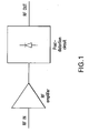
- FIG. 1 A block diagram of this invention is shown in Figure 1 . It consists of a nonlinear device (in this case RF amplifier, but it would also apply to an optical receiver) followed by a post-distortion circuit that generates distortion such as to cancel the distortion from the previous nonlinear device.
- a nonlinear device in this case RF amplifier, but it would also apply to an optical receiver
- this could be a single-ended amplifier with only one transistor, with low DC operating current and low supply voltage.
- the circuit could also include a photodiode operating from a low supply voltage.
- the amplifying transistors When operated with low quiescent voltages and/or currents, the amplifying transistors produce distortion, which can be both real and imaginary.
- One or various post-distortion circuits can be added after the amplification stage to cancel the distortion.
- Real distortion is typically cancelled with Schottky diodes.
- Imaginary distortion is typically cancelled using varactor diodes, or adding reactive components to the Schottky diode circuits.
- Reactive components can also be added to the post-distortion circuits in order to alter the frequency dependence of the distortion.
- the quiescent voltages and/or currents of the amplifying transistors can also be adjusted in order to match the magnitude, phase and frequency content of the distortion generated by the post-distortion circuit.
- Circuits that generate second order distortion typically generate third order distortion as well.
- the circuits can be designed so that both second order and third order distortion is cancelled simultaneously. Alternatively, one can design a circuit in a push-pull configuration that only cancels third order distortion and
- the amplifier and post-distortion circuit can be packaged together with the photodiode in order to reduce parasitics.
- either the post-distortion circuit or both amplifier and post-distortion circuits can be mounted outside the photodiode package on a circuit board.
- Figure 2 shows a demonstration of a TIA in PHEMPT technology according to the present invention.
- the results show second order distortion (IMD2) and third order distortion (IMD3) using a two tone test with laser modulation index 40% and total optical input power 1 dBm.
- IMD2 second order distortion
- IMD3 third order distortion
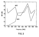
- Figure 3 shows distortion for an amplifier with post-distortion according to the present invention.
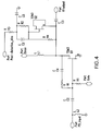
- Figure 4 is an exemplary embodiment of an optical receiver according to the present invention. Both amplifier and post-distortion sections could be combined in an IC using PHEMT technology for low cost and high performance.
- the amplification stage is represented by transistor Q1.
- the postdistortion stage merely consists of transistor Q2 acting as a Schottky diode.
- Resistor R4 is added in order to reduce the third order distortion generated by the postdistortion circuit, which could be undesirable.
- Resistor R2 controls the amount of postdistortion generated by the circuit, and capacitor C2 is used to adjust the phase of the distortion.
- the amount of second and third order distortion is also controlled by adjusting the postdistortion bias voltage.
- Figure 5 is another exemplary embodiment of an optical receiver according to the present invention.
- the postdistortion circuit consists of a Schottky diode and a varactor diode, so as to provide flexible cancellation of real and imaginary distortion as described previously. If the real part of the amplifier distortion is negative, then the cathode terminal of the Schottky diode should be connected to the main transmission path, as shown in Figure 5 . If the real part of the amplifier distortion is positive, then the anode terminal of the Schottky diode should be connected to the main transmission path. If the imaginary part of the amplifier distortion is negative, then the cathode terminal of the varactor diode should be connected to capacitor C22, as shown in Figure 5 . If the imaginary part of the amplifier distortion is positive, then the anode terminal of the varactor diode should be connected to capacitor C22.
- Figure 6 is yet another exemplary block diagram of an optical receiver according to the present invention.
- the first amplification stage follows the photodiode, and uses post-distortion to correct for the distortion, i.e. the correction circuit follows the amplification circuit.
- the first amplification stage and post-distortion circuits could possibly correspond to circuits presented in either Figure 4 or 5 .
- the fmal amplification stage uses pre-distortion, i.e. the correction circuit goes prior to the amplification circuit. Between these amplification stages there might be an additional stage for impedance matching and/or gain control. Additional amplification stages can me added for higher gain, either with pre- or post- distortion.
Landscapes
- Engineering & Computer Science (AREA)
- Physics & Mathematics (AREA)
- Power Engineering (AREA)
- Electromagnetism (AREA)
- Computer Networks & Wireless Communication (AREA)
- Signal Processing (AREA)
- Nonlinear Science (AREA)
- Amplifiers (AREA)
- Optical Communication System (AREA)
Abstract
Description
- This application is related to
U.S. Patent Application Serial No. 11/148,022 filed June 9, 2005 - The invention relates to optical receivers, and in particular to RF amplifiers that have a non-linear operating characteristic and interface between a photodiode that receives an optical signal from an optical fiber, such as used in fiber optical communications links, and electronic network terminal units.
- A variety of optical communications systems are known in the art which include an optical transmit portion that converts an electrical signal into an optical signal launched into an optical fiber, and a receive portion that receives an optical signal from the optical fiber and converts it into an electrical signal. Traditionally, optical receive sections include an optical assembly to focus or direct the light from the optical fiber onto a photodetector, which in turn, is connected to an amplifier/limiter circuit on a circuit board. The photodetector or photodiode is typically packaged in a hermetically sealed package in order to protect it from harsh environmental conditions. The photodiodes are semiconductor chips that are typically a few hundred microns to a couple of millimeters wide and 100-500 microns thick. The package in which they are mounted is typically from three to six millimeters in diameter, and two to five millimeters tall and has several electrical leads coming out of the package. These electrical leads are then soldered to the circuit board containing the amplifier/limiter and other circuits for processing the electrical signal.
- Fiber optic transmission has been used for many years for the distribution of analog CATV signals. Optical receivers for analog CATV signals typically consist of a packaged photodiode electrically connected to a separately-packaged low-noise electronic amplifier, with the photodiode package usually consisting of a TO can with an optical window cap of a ball lens cap to allow light from an optical fiber to be coupled to the photodiode.
- A disadvantage of the above arrangement is that there are significant parasitic capacitances associated with the separate photodiode and electronic amplifier packages. These parasitic capacitances play a role in limiting the performance of the optical receiver, resulting in lower bandwidth and higher noise, and contributing to higher power dissipation required to meet a particular target specification.
- Distribution of analog CATV signals is particularly challenging because of the high degree of linearity required to obtain adequate quality. Two techniques have been employed previously to obtain this level of low electrical distortion.
- Operating the amplifying transistors with high quiescent currents and voltages so that the signal swing is limited to a small fraction of the available current or voltage excursion. These high quiescent voltages and currents lead to high DC power dissipation.
- Use of a push-pull or balanced amplifiers, which cancel even-order distortion products are also known. Push-pull amplifiers also come at the price of higher power dissipation, however, because two amplifiers are needed instead of just one single-ended amplifier, and also at the price of balanced-to-unbalanced transformers needed to interconnect to later single-ended stages.
- Another technique that has been used in CATV systems is pre-distortion. Here an electrical signal is generated prior to the nonlinear element such that it cancels the distortion of the nonlinear element. This has been mainly applied to linearize lasers.
US6288814 ,US2005/0195038 , andUS5600472 exemplity such prior art. - For new Fiber-to-the-Home applications that include an analog optical CATV receiver at each customer premise, there is a strong desire on the part of system suppliers and operating companies to reduce power dissipation and to lower device cost.
- It is an object of the present invention to provide an optical receiver with distortion cancellation for use with optical network system units such as receivers and transceivers.
- It is also another aspect of the present invention to provide a distortion cancellation circuit for use in non-linear amplifiers used in analog RF transmission systems.
- Briefly, and in general terms, the present invention provides an optical receiver for converting and coupling an information-containing optical signal from an optical fiber, including a photodiode subassembly in the housing for converting an optical signal into a modulated electrical signal corresponding to the optical signal; and an amplifier including a distortion cancellation circuit. More specifically, the invention provides an optical receives according to claim 1.
- Additional objects, advantages, and novel features of the present invention will become apparent to those skilled in the art from this disclosure, including the following detailed description as well as by practice of the invention. While the invention is described below with reference to preferred embodiments, it should be understood that the invention is not limited thereto. Those of ordinary skill in the art having access to the teachings herein will recognize additional applications, modifications and embodiments in other fields, which are within the scope of the invention as disclosed and claimed herein with respect to which the invention could be of utility.
- These and other features of the present invention will be better understood and more fully appreciated by reference to the following detailed description when considered in conjunction with the accompanying drawings, wherein:
-
FIG. 1 is a block diagram of an amplifier in an exemplary embodiment in accordance with the present invention; -
FIG. 2 is a graph of the distortion of an optical receiver with a single diode distortion cancellation circuit in an exemplary embodiment in accordance with the present invention; -
FIG. 3 is a graph of the distortion of an amplifier with a single diode post-distortion cancellation circuit in an exemplary embodiment in accordance with the present invention; -
FIG. 4 is an exemplary embodiment of the present invention as an integrated circuit in PHEMT technology. -
FIG. 5 is a block diagram of the present invention using two circuits to achieve cancellation of real and imaginary distortion. -
FIG. 6 is an exemplary embodiment of the present invention with two stages of amplification. - The first amplification stage of an optical receiver usually consists of a transimpedance amplifier, also known as TIA, such that the receiver noise is minimized. In order to achieve high linearity and low electrical distortion required for analog applications, the amplifying transistors are operated with high quiescent currents and voltages so that the signal swing is limited to a small fraction of the available current or voltage excursion. These high quiescent voltages and currents lead to the high DC powerdissipation of analog TIAs.
- A block diagram of this invention is shown in
Figure 1 . It consists of a nonlinear device (in this case RF amplifier, but it would also apply to an optical receiver) followed by a post-distortion circuit that generates distortion such as to cancel the distortion from the previous nonlinear device. In the case of an amplifier, this could be a single-ended amplifier with only one transistor, with low DC operating current and low supply voltage. In the case of an optical receiver, the circuit could also include a photodiode operating from a low supply voltage. - When operated with low quiescent voltages and/or currents, the amplifying transistors produce distortion, which can be both real and imaginary. One or various post-distortion circuits can be added after the amplification stage to cancel the distortion. Real distortion is typically cancelled with Schottky diodes. Imaginary distortion is typically cancelled using varactor diodes, or adding reactive components to the Schottky diode circuits. Reactive components can also be added to the post-distortion circuits in order to alter the frequency dependence of the distortion. The quiescent voltages and/or currents of the amplifying transistors can also be adjusted in order to match the magnitude, phase and frequency content of the distortion generated by the post-distortion circuit. Circuits that generate second order distortion typically generate third order distortion as well. The circuits can be designed so that both second order and third order distortion is cancelled simultaneously. Alternatively, one can design a circuit in a push-pull configuration that only cancels third order distortion and a separate circuit to cancel second order distortion.
- The amplifier and post-distortion circuit can be packaged together with the photodiode in order to reduce parasitics. Alternatively, either the post-distortion circuit or both amplifier and post-distortion circuits can be mounted outside the photodiode package on a circuit board.
- There is a distinct advantage in using post-distortion rather than pre-distortion when correcting the distortion of a small-signal amplifier. Since the input power to the distortion circuit is higher, large levels of correction are easier to achieve with low loss. In the case of an optical receiver, you can only use post-distortion as the input signal levels are too low for pre-distortion to work.
-
Figure 2 shows a demonstration of a TIA in PHEMPT technology according to the present invention. The results show second order distortion (IMD2) and third order distortion (IMD3) using a two tone test with laser modulation index 40% and total optical input power 1 dBm. -
Figure 3 shows distortion for an amplifier with post-distortion according to the present invention. -
Figure 4 is an exemplary embodiment of an optical receiver according to the present invention. Both amplifier and post-distortion sections could be combined in an IC using PHEMT technology for low cost and high performance. - The amplification stage is represented by transistor Q1. In this embodiment, the postdistortion stage merely consists of transistor Q2 acting as a Schottky diode. Resistor R4 is added in order to reduce the third order distortion generated by the postdistortion circuit, which could be undesirable. Resistor R2 controls the amount of postdistortion generated by the circuit, and capacitor C2 is used to adjust the phase of the distortion. The amount of second and third order distortion is also controlled by adjusting the postdistortion bias voltage.
-
Figure 5 is another exemplary embodiment of an optical receiver according to the present invention. In this case the postdistortion circuit consists of a Schottky diode and a varactor diode, so as to provide flexible cancellation of real and imaginary distortion as described previously. If the real part of the amplifier distortion is negative, then the cathode terminal of the Schottky diode should be connected to the main transmission path, as shown inFigure 5 . If the real part of the amplifier distortion is positive, then the anode terminal of the Schottky diode should be connected to the main transmission path. If the imaginary part of the amplifier distortion is negative, then the cathode terminal of the varactor diode should be connected to capacitor C22, as shown inFigure 5 . If the imaginary part of the amplifier distortion is positive, then the anode terminal of the varactor diode should be connected to capacitor C22. -
Figure 6 is yet another exemplary block diagram of an optical receiver according to the present invention. The first amplification stage follows the photodiode, and uses post-distortion to correct for the distortion, i.e. the correction circuit follows the amplification circuit. The first amplification stage and post-distortion circuits could possibly correspond to circuits presented in eitherFigure 4 or5 . The fmal amplification stage uses pre-distortion, i.e. the correction circuit goes prior to the amplification circuit. Between these amplification stages there might be an additional stage for impedance matching and/or gain control. Additional amplification stages can me added for higher gain, either with pre- or post- distortion. - Even though this invention has been described within the context of CATV and FTTX applications, it could benefit many other applications that might require highly linear RF and/or optoelectronic components such as, but not limited to, satellite communications, radar systems and military applications.
Claims (9)
- (Currently Amended) An optical receiver comprising:a photodetector coupled to an external optical fiber for receiving an optical communications signal and converting it into an electrical signal;a single ended RF amplifier with only one transistor (Q1) coupled to the electrical output of the photodetector and generating an output signal with distortion;a first inductor coupled to a first capacitor (C1) coupled to an input of the single ended RF amplifier (Q1);a second inductor coupled to an output of the single ended RF amplifier (Q1) ;a resistor (R) having a first terminal and a second terminal, the first terminal being coupled to the input of the single ended RF amplifier (Q1) ;a second capacitor (C4) having a first terminal and a second terminal, the first terminal being coupled to the second terminal of the resistor (R) and the second terminal being coupled to the output of the single ended RF amplifier (Q1) anda post-distortion circuit (Q2) including a Schottky diode connected to the output of the RF amplifier (Q1) for canceling the distortion in the output signal produced by the RF amplifier, wherein the single ended RF amplifier (Q1) and the post-distortion circuit (Q2) are in single package. .
- An optical receiver as defined in claim 1, wherein the single package is formed by an integrated chip (IC).
- An optical receiver as defined in claim 1, wherein the post-distortion circuit for canceling distortion further includes a varactor diode.
- An optical receiver as defined in claim 1, wherein the post-distortion circuit for canceling distortion includes a transistor.
- An optical receiver as defined in claim 1, wherein the post-distortion circuit for canceling distortion includes at least a resistor and a capacitor for adjusting magnitude, and phase content of the distortion generated by the RF amplifier.
- An optical receiver as defined in claim 1, further comprising means for adjusting a DC operating point of a nonlinear device in order to tune the distortion.
- An optical receiver as defined in claim 1, wherein the post-distortion circuit cancels both second and third order distortion.
- An optical receiver as defined in claim 1, wherein the single ended RF amplifier is followed by one or more amplification stages using pre and/or post-distortion.
- An optical receiver as defined in claim 1, wherein the single package includes a first port coupled to the first inductor for the input of the single ended RF amplifier, a second port for a gate of the only one transistor, a third port coupled to the second inductor for a drain of the only one transistor, a fourth port for a bias voltage coupled to the Schottky diode, and a fifth port for an output of the post-distortion circuit.
Applications Claiming Priority (1)
| Application Number | Priority Date | Filing Date | Title |
|---|---|---|---|
| US11/262,077 US7596326B2 (en) | 2005-10-27 | 2005-10-27 | Distortion cancellation circuitry for optical receivers |
Publications (2)
| Publication Number | Publication Date |
|---|---|
| EP1783933A1 EP1783933A1 (en) | 2007-05-09 |
| EP1783933B1 true EP1783933B1 (en) | 2010-05-19 |
Family
ID=37800975
Family Applications (1)
| Application Number | Title | Priority Date | Filing Date |
|---|---|---|---|
| EP06015988A Not-in-force EP1783933B1 (en) | 2005-10-27 | 2006-08-01 | Distortion cancellation circuitry for optical receivers |
Country Status (6)
| Country | Link |
|---|---|
| US (1) | US7596326B2 (en) |
| EP (1) | EP1783933B1 (en) |
| JP (1) | JP2007124659A (en) |
| CN (1) | CN1960216B (en) |
| AT (1) | ATE468667T1 (en) |
| DE (1) | DE602006014343D1 (en) |
Families Citing this family (6)
| Publication number | Priority date | Publication date | Assignee | Title |
|---|---|---|---|---|
| US7634198B2 (en) * | 2006-06-21 | 2009-12-15 | Emcore Corporation | In-line distortion cancellation circuits for linearization of electronic and optical signals with phase and frequency adjustment |
| US8260144B2 (en) * | 2008-03-12 | 2012-09-04 | Hypres Inc. | Digital radio frequency tranceiver system and method |
| US8660437B1 (en) * | 2010-11-24 | 2014-02-25 | Emcore Corporation | Minimizing distortion due to wavelength dependent loss in WDM optical networks |
| WO2015160660A1 (en) * | 2014-04-15 | 2015-10-22 | Arris Enterprises, Inc. | Smart receivers and transmitters for catv networks |
| US10566937B2 (en) * | 2016-12-16 | 2020-02-18 | Qualcomm Incorporated | Post distortion cancellation with phase shifter diode for low noise amplifier |
| KR102538339B1 (en) | 2019-01-07 | 2023-05-31 | 삼성전자 주식회사 | An amplifier with linearization using post-distortion |
Family Cites Families (73)
| Publication number | Priority date | Publication date | Assignee | Title |
|---|---|---|---|---|
| US4075474A (en) * | 1977-04-19 | 1978-02-21 | Northern Telecom Limited | Method and apparatus for distortion reduction in optical communication systems |
| FR2410907A1 (en) * | 1977-12-02 | 1979-06-29 | Thomson Csf | DISTORTION CORRECTOR FOR HYPERFREQUENCY TUBES |
| US4277763A (en) * | 1978-02-21 | 1981-07-07 | Ward Jr William H | Non-linear predistortion linearizing circuit for a varactor diode tuned oscillator |
| US4700151A (en) * | 1985-03-20 | 1987-10-13 | Nec Corporation | Modulation system capable of improving a transmission system |
| US4633197A (en) * | 1985-03-29 | 1986-12-30 | Motorola, Inc. | Single resonant tank modulated oscillator |
| US4752743A (en) * | 1986-09-26 | 1988-06-21 | Varian Associates, Inc. | Linearizer for TWT amplifiers |
| CA1280180C (en) * | 1987-02-02 | 1991-02-12 | Masatoshi Ishida | Nonlinear signal generating circuit and nonlinear compensating deviceusing the same |
| GB2204202B (en) * | 1987-04-28 | 1991-11-27 | Racal Communications Equip | Radio transmitters |
| US4882482A (en) | 1988-10-26 | 1989-11-21 | Tektronix, Inc. | Thermally stabilized optical preamplifier |
| US5161044A (en) * | 1989-07-11 | 1992-11-03 | Harmonic Lightwaves, Inc. | Optical transmitters linearized by means of parametric feedback |
| US5363056A (en) * | 1989-09-07 | 1994-11-08 | Ortel Corporation | Circuit for linearization of amplified electronic signals |
| US4992754B1 (en) * | 1989-09-07 | 1997-10-28 | Ortel Corp | Predistorter for linearization of electronic and optical signals |
| US5132639A (en) * | 1989-09-07 | 1992-07-21 | Ortel Corporation | Predistorter for linearization of electronic and optical signals |
| US5252930A (en) * | 1989-09-07 | 1993-10-12 | Ortel Corporation | Predistorter for linearization of electronic and optical signals |
| US5038113A (en) * | 1989-12-01 | 1991-08-06 | General Electric Company | Nonlinearity generator using FET source-to-drain conductive path |
| US5239402A (en) * | 1989-12-01 | 1993-08-24 | Scientific-Atlanta, Inc. | Push-pull optical receiver |
| IT1239472B (en) * | 1990-04-09 | 1993-11-02 | Sits Soc It Telecom Siemens | LINEARIZER OF THE PRE-DISTORTION TYPE FOR MICROWAVE POWER AMPLIFIERS |
| US5049832A (en) * | 1990-04-20 | 1991-09-17 | Simon Fraser University | Amplifier linearization by adaptive predistortion |
| US5113068A (en) * | 1990-12-28 | 1992-05-12 | Square D Company | Photoelectrical sensor with multistaged, filtered amplifier circuit |
| DE4121570A1 (en) * | 1991-06-29 | 1993-01-07 | Standard Elektrik Lorenz Ag | EQUALIZER FOR OPTICAL MESSAGE TRANSMISSION SYSTEMS |
| EP0524758B1 (en) | 1991-07-23 | 1998-10-28 | AT&T Corp. | Distortion compensation for analog optical systems |
| US5146177A (en) * | 1991-08-30 | 1992-09-08 | General Electric Co. | Balanced reflective nonlinear processor using FETs |
| US5436749A (en) * | 1991-12-09 | 1995-07-25 | Scientific-Atlanta, Inc. | Method and apparatus for predistortion |
| US5342389A (en) * | 1992-04-28 | 1994-08-30 | Habley Medical Technology Corporation | Tissue manipulator |
| US5430569A (en) * | 1992-05-22 | 1995-07-04 | Ortel Corporation | Suppression of noise and distortion in fiber-optic systems |
| FR2694862B1 (en) * | 1992-08-14 | 1994-09-16 | Cit Alcatel | Predistortion semiconductor optical source. |
| US5481389A (en) * | 1992-10-09 | 1996-01-02 | Scientific-Atlanta, Inc. | Postdistortion circuit for reducing distortion in an optical communications system |
| SG52501A1 (en) * | 1992-10-21 | 1998-09-28 | At & T Corp | Cascaded distortion compensation for analog optical systems |
| GB2272589B (en) * | 1992-11-16 | 1995-11-29 | Linear Modulation Tech | Automatic calibration of the quadrature balance within a cartesian amplifier |
| US5430568A (en) * | 1992-12-01 | 1995-07-04 | Scientific-Atlanta, Inc. | Optical communications system for transmitting information signals having different wavelengths over a same optical fiber |
| US5477367A (en) * | 1992-12-04 | 1995-12-19 | U.S. Philips Corporation | Optical transmission system |
| CA2120965A1 (en) | 1993-04-14 | 1994-10-15 | Katsumi Uesaka | Distortion generating circuit |
| US5321710A (en) * | 1993-04-19 | 1994-06-14 | Raynet Corporation | Predistortion method and apparatus for laser linearization |
| US5424680A (en) * | 1993-11-30 | 1995-06-13 | Harmonic Lightwaves, Inc. | Predistorter for high frequency optical communications devices |
| US5428314A (en) * | 1994-05-09 | 1995-06-27 | Tacan Corporation | Odd/even order distortion generator and distortion cancellation circuit |
| US5798854A (en) * | 1994-05-19 | 1998-08-25 | Ortel Corporation | In-line predistorter for linearization of electronic and optical signals |
| WO1995032561A1 (en) | 1994-05-19 | 1995-11-30 | Ortel Corporation | In-line predistorter for linearization of electronic and optical signals |
| US6288814B1 (en) * | 1994-05-19 | 2001-09-11 | Ortel Corporation | In-line predistorter for linearization of electronic and optical signals |
| US5523716A (en) * | 1994-10-13 | 1996-06-04 | Hughes Aircraft Company | Microwave predistortion linearizer |
| US5606286A (en) * | 1995-07-27 | 1997-02-25 | Bains; Devendar S. | Predistortion linearization |
| US5589797A (en) * | 1995-09-26 | 1996-12-31 | Lucent Technologies Inc. | Low distortion amplifier |
| JP3528998B2 (en) * | 1996-01-09 | 2004-05-24 | 松下電器産業株式会社 | Optical transmission system and optical transmission method |
| US5699179A (en) * | 1996-02-23 | 1997-12-16 | General Instrument Corporation Of Delaware | Cancellation of distortion components in a fiber optic link with feed-forward linearization |
| JP3545125B2 (en) * | 1996-03-08 | 2004-07-21 | 富士通株式会社 | Distortion compensation circuit |
| US6055278A (en) * | 1996-04-26 | 2000-04-25 | C-Cor.Net Corporation | Linearization circuits and methods |
| US5812294A (en) * | 1996-06-03 | 1998-09-22 | Lucent Technologies Inc. | Linearized optical transmitter |
| JP3022347B2 (en) * | 1996-10-18 | 2000-03-21 | 八木アンテナ株式会社 | Distortion compensation circuit |
| US5850305A (en) * | 1996-12-18 | 1998-12-15 | Scientific-Atlanta, Inc. | Adaptive predistortion control for optical external modulation |
| US5963352A (en) * | 1997-02-21 | 1999-10-05 | Scientific-Atlanta, Inc. | Linearization enhanced operation of single-stage and dual-stage electro-optic modulators |
| US6122085A (en) * | 1997-04-08 | 2000-09-19 | Lucent Technologies Inc. | Lightwave transmission techniques |
| CA2202458C (en) * | 1997-04-11 | 2001-02-06 | Surinder Kumar | Direct qam modulator |
| CA2289511A1 (en) * | 1997-05-12 | 1998-11-19 | Pirelli Cavi E Sistemi S.P.A. | External optical modulation system comprising a predistorter |
| TW336363B (en) * | 1997-06-20 | 1998-07-11 | New Elite Technologies Inc | Distortion compensation device for broadband fiber optic transmission system |
| CN1160869C (en) * | 1997-09-25 | 2004-08-04 | 皇家菲利浦电子有限公司 | Improved phase receiver |
| US6133790A (en) * | 1998-09-17 | 2000-10-17 | Motorola, Inc. | In-line, unbalanced amplifier, predistortion circuit |
| US6018266A (en) * | 1998-11-18 | 2000-01-25 | Hughes Electronics Corporation | Radio frequency system having reflective diode linearizer with balanced tunable impedance loads |
| US6549316B2 (en) * | 1998-12-15 | 2003-04-15 | Agere Systems, Inc. | Circuit for suppressing noise and distortion in linear fiber optic links |
| US6519374B1 (en) * | 1999-03-30 | 2003-02-11 | Uniphase Corporation | Predistortion arrangement using mixers in nonlinear electro-optical applications |
| AU770446B2 (en) * | 1999-04-01 | 2004-02-19 | General Instrument Corporation | Non-linear distortion generator |
| US6204718B1 (en) * | 1999-06-25 | 2001-03-20 | Scientific-Atlanta, Inc. | Method and apparatus for generating second-order predistortion without third-order distortion |
| US6255908B1 (en) * | 1999-09-03 | 2001-07-03 | Amplix | Temperature compensated and digitally controlled amplitude and phase channel amplifier linearizer for multi-carrier amplification systems |
| WO2001043278A1 (en) | 1999-12-10 | 2001-06-14 | General Instrument Corporation | Low distortion transimpedance amplifier using distortion cancellation technique |
| US6388470B1 (en) * | 2000-03-30 | 2002-05-14 | Philips Electronics North American Corporation | High voltage CMOS signal driver with minimum power dissipation |
| CN1233090C (en) * | 2000-08-11 | 2005-12-21 | 新加坡国立大学 | Programmable radio frequency pre-compensation linear circuit and its method |
| KR100350320B1 (en) * | 2000-11-30 | 2002-08-28 | 주식회사 에이앤피텔레콤 | Method and Apparatus for Removing Non-Linear Distortion in a Optic Transmitter |
| JP2002368546A (en) * | 2001-06-06 | 2002-12-20 | Nec Corp | Distortion pre-compensator and linear amplifier using the same |
| US6542037B2 (en) * | 2001-08-09 | 2003-04-01 | Tyco Electronics Corp. | Low distortion broadband amplifier using GaAs pHEMT devices |
| US6985020B2 (en) * | 2002-07-09 | 2006-01-10 | General Instrument Corporation | Inline predistortion for both CSO and CTB correction |
| US6806778B1 (en) * | 2003-02-18 | 2004-10-19 | Sirenza Microdevices, Inc. | Darlington cascode |
| US7340184B2 (en) * | 2003-05-01 | 2008-03-04 | Optium Corporation | Linearized Optical Transmitter Using Feedback Control |
| US7388435B2 (en) * | 2003-12-05 | 2008-06-17 | Parsec Technologies, Inc. | Linearized trans-impedance amplifier |
| EP1779558B1 (en) * | 2004-08-12 | 2012-11-28 | Triaccess Technologies, Inc | Level detector for optical receivers |
| US20070003291A1 (en) | 2005-06-09 | 2007-01-04 | Kasper Bryon L | Distortion cancellation in a transimpedance amplifier circuit |
-
2005
- 2005-10-27 US US11/262,077 patent/US7596326B2/en not_active Expired - Fee Related
-
2006
- 2006-08-01 AT AT06015988T patent/ATE468667T1/en not_active IP Right Cessation
- 2006-08-01 EP EP06015988A patent/EP1783933B1/en not_active Not-in-force
- 2006-08-01 DE DE602006014343T patent/DE602006014343D1/en active Active
- 2006-09-04 CN CN2006101286711A patent/CN1960216B/en not_active Expired - Fee Related
- 2006-10-26 JP JP2006290849A patent/JP2007124659A/en active Pending
Also Published As
| Publication number | Publication date |
|---|---|
| JP2007124659A (en) | 2007-05-17 |
| DE602006014343D1 (en) | 2010-07-01 |
| CN1960216A (en) | 2007-05-09 |
| CN1960216B (en) | 2012-07-04 |
| US7596326B2 (en) | 2009-09-29 |
| US20070098417A1 (en) | 2007-05-03 |
| EP1783933A1 (en) | 2007-05-09 |
| ATE468667T1 (en) | 2010-06-15 |
Similar Documents
| Publication | Publication Date | Title |
|---|---|---|
| US20060182449A1 (en) | Optical transmitter with integrated amplifier and pre-distortion circuit | |
| US7418213B2 (en) | Transimpedance amplifier with integrated filtering and reduced parasitic capacitance | |
| US20200091881A1 (en) | Differential trans-impedance amplifier | |
| US7755433B2 (en) | Preamplifier and optical receiving device including the same | |
| US20110311232A1 (en) | Optical receiver and optical transmission system | |
| KR20070121516A (en) | Inline distortion cancellation circuit for linearization of electronic and optical signals by phase and frequency adjustment | |
| US20190132163A1 (en) | Dc offset cancellation and crosspoint control circuit | |
| US6879217B2 (en) | Triode region MOSFET current source to bias a transimpedance amplifier | |
| US8222590B2 (en) | Signal amplifier for optical receiver circuit | |
| US9054655B2 (en) | Transimpedance amplifier | |
| US7596326B2 (en) | Distortion cancellation circuitry for optical receivers | |
| US20030002551A1 (en) | Laser diode driver | |
| US20050052248A1 (en) | Elevated front-end transimpedance amplifier | |
| EP1732209A1 (en) | Distortion cancellation in a transimpedance amplifier circuit | |
| US5095286A (en) | Fiber optic receiver and amplifier | |
| US7504889B2 (en) | Circuit for providing a signal boost | |
| WO2002045303A1 (en) | Method and apparatus for removing non-linear distortion in optic transmitter | |
| US6714082B2 (en) | Semiconductor amplifier circuit | |
| US20230291366A1 (en) | Transimpedance amplifier circuits and devices | |
| US10756512B2 (en) | Driving circuit and optical module | |
| CN111527443A (en) | Optical signal modulator comprising a feedback loop | |
| US20040174221A1 (en) | Preamplification circuit | |
| JP5798051B2 (en) | Optical transmission circuit | |
| US7860407B2 (en) | Pre-emphasis circuit | |
| Vettiger | Linear signal transmission with optocouplers |
Legal Events
| Date | Code | Title | Description |
|---|---|---|---|
| PUAI | Public reference made under article 153(3) epc to a published international application that has entered the european phase |
Free format text: ORIGINAL CODE: 0009012 |
|
| AK | Designated contracting states |
Kind code of ref document: A1 Designated state(s): AT BE BG CH CY CZ DE DK EE ES FI FR GB GR HU IE IS IT LI LT LU LV MC NL PL PT RO SE SI SK TR |
|
| AX | Request for extension of the european patent |
Extension state: AL BA HR MK YU |
|
| 17P | Request for examination filed |
Effective date: 20071030 |
|
| AKX | Designation fees paid |
Designated state(s): AT BE BG CH CY CZ DE DK EE ES FI FR GB GR HU IE IS IT LI LT LU LV MC NL PL PT RO SE SI SK TR |
|
| 17Q | First examination report despatched |
Effective date: 20080806 |
|
| GRAP | Despatch of communication of intention to grant a patent |
Free format text: ORIGINAL CODE: EPIDOSNIGR1 |
|
| GRAS | Grant fee paid |
Free format text: ORIGINAL CODE: EPIDOSNIGR3 |
|
| GRAA | (expected) grant |
Free format text: ORIGINAL CODE: 0009210 |
|
| AK | Designated contracting states |
Kind code of ref document: B1 Designated state(s): AT BE BG CH CY CZ DE DK EE ES FI FR GB GR HU IE IS IT LI LT LU LV MC NL PL PT RO SE SI SK TR |
|
| REG | Reference to a national code |
Ref country code: GB Ref legal event code: FG4D |
|
| REG | Reference to a national code |
Ref country code: CH Ref legal event code: EP |
|
| REG | Reference to a national code |
Ref country code: IE Ref legal event code: FG4D |
|
| REF | Corresponds to: |
Ref document number: 602006014343 Country of ref document: DE Date of ref document: 20100701 Kind code of ref document: P |
|
| REG | Reference to a national code |
Ref country code: NL Ref legal event code: VDEP Effective date: 20100519 |
|
| LTIE | Lt: invalidation of european patent or patent extension |
Effective date: 20100519 |
|
| PG25 | Lapsed in a contracting state [announced via postgrant information from national office to epo] |
Ref country code: ES Free format text: LAPSE BECAUSE OF FAILURE TO SUBMIT A TRANSLATION OF THE DESCRIPTION OR TO PAY THE FEE WITHIN THE PRESCRIBED TIME-LIMIT Effective date: 20100830 Ref country code: LT Free format text: LAPSE BECAUSE OF FAILURE TO SUBMIT A TRANSLATION OF THE DESCRIPTION OR TO PAY THE FEE WITHIN THE PRESCRIBED TIME-LIMIT Effective date: 20100519 Ref country code: SE Free format text: LAPSE BECAUSE OF FAILURE TO SUBMIT A TRANSLATION OF THE DESCRIPTION OR TO PAY THE FEE WITHIN THE PRESCRIBED TIME-LIMIT Effective date: 20100519 |
|
| PG25 | Lapsed in a contracting state [announced via postgrant information from national office to epo] |
Ref country code: AT Free format text: LAPSE BECAUSE OF FAILURE TO SUBMIT A TRANSLATION OF THE DESCRIPTION OR TO PAY THE FEE WITHIN THE PRESCRIBED TIME-LIMIT Effective date: 20100519 Ref country code: FI Free format text: LAPSE BECAUSE OF FAILURE TO SUBMIT A TRANSLATION OF THE DESCRIPTION OR TO PAY THE FEE WITHIN THE PRESCRIBED TIME-LIMIT Effective date: 20100519 Ref country code: SI Free format text: LAPSE BECAUSE OF FAILURE TO SUBMIT A TRANSLATION OF THE DESCRIPTION OR TO PAY THE FEE WITHIN THE PRESCRIBED TIME-LIMIT Effective date: 20100519 Ref country code: IS Free format text: LAPSE BECAUSE OF FAILURE TO SUBMIT A TRANSLATION OF THE DESCRIPTION OR TO PAY THE FEE WITHIN THE PRESCRIBED TIME-LIMIT Effective date: 20100919 Ref country code: LV Free format text: LAPSE BECAUSE OF FAILURE TO SUBMIT A TRANSLATION OF THE DESCRIPTION OR TO PAY THE FEE WITHIN THE PRESCRIBED TIME-LIMIT Effective date: 20100519 |
|
| PG25 | Lapsed in a contracting state [announced via postgrant information from national office to epo] |
Ref country code: PL Free format text: LAPSE BECAUSE OF FAILURE TO SUBMIT A TRANSLATION OF THE DESCRIPTION OR TO PAY THE FEE WITHIN THE PRESCRIBED TIME-LIMIT Effective date: 20100519 Ref country code: GR Free format text: LAPSE BECAUSE OF FAILURE TO SUBMIT A TRANSLATION OF THE DESCRIPTION OR TO PAY THE FEE WITHIN THE PRESCRIBED TIME-LIMIT Effective date: 20100820 Ref country code: CY Free format text: LAPSE BECAUSE OF FAILURE TO SUBMIT A TRANSLATION OF THE DESCRIPTION OR TO PAY THE FEE WITHIN THE PRESCRIBED TIME-LIMIT Effective date: 20100519 |
|
| PG25 | Lapsed in a contracting state [announced via postgrant information from national office to epo] |
Ref country code: EE Free format text: LAPSE BECAUSE OF FAILURE TO SUBMIT A TRANSLATION OF THE DESCRIPTION OR TO PAY THE FEE WITHIN THE PRESCRIBED TIME-LIMIT Effective date: 20100519 Ref country code: DK Free format text: LAPSE BECAUSE OF FAILURE TO SUBMIT A TRANSLATION OF THE DESCRIPTION OR TO PAY THE FEE WITHIN THE PRESCRIBED TIME-LIMIT Effective date: 20100519 Ref country code: NL Free format text: LAPSE BECAUSE OF FAILURE TO SUBMIT A TRANSLATION OF THE DESCRIPTION OR TO PAY THE FEE WITHIN THE PRESCRIBED TIME-LIMIT Effective date: 20100519 Ref country code: PT Free format text: LAPSE BECAUSE OF FAILURE TO SUBMIT A TRANSLATION OF THE DESCRIPTION OR TO PAY THE FEE WITHIN THE PRESCRIBED TIME-LIMIT Effective date: 20100920 |
|
| PG25 | Lapsed in a contracting state [announced via postgrant information from national office to epo] |
Ref country code: SK Free format text: LAPSE BECAUSE OF FAILURE TO SUBMIT A TRANSLATION OF THE DESCRIPTION OR TO PAY THE FEE WITHIN THE PRESCRIBED TIME-LIMIT Effective date: 20100519 Ref country code: RO Free format text: LAPSE BECAUSE OF FAILURE TO SUBMIT A TRANSLATION OF THE DESCRIPTION OR TO PAY THE FEE WITHIN THE PRESCRIBED TIME-LIMIT Effective date: 20100519 Ref country code: CZ Free format text: LAPSE BECAUSE OF FAILURE TO SUBMIT A TRANSLATION OF THE DESCRIPTION OR TO PAY THE FEE WITHIN THE PRESCRIBED TIME-LIMIT Effective date: 20100519 Ref country code: BE Free format text: LAPSE BECAUSE OF FAILURE TO SUBMIT A TRANSLATION OF THE DESCRIPTION OR TO PAY THE FEE WITHIN THE PRESCRIBED TIME-LIMIT Effective date: 20100519 |
|
| PLBE | No opposition filed within time limit |
Free format text: ORIGINAL CODE: 0009261 |
|
| STAA | Information on the status of an ep patent application or granted ep patent |
Free format text: STATUS: NO OPPOSITION FILED WITHIN TIME LIMIT |
|
| PG25 | Lapsed in a contracting state [announced via postgrant information from national office to epo] |
Ref country code: MC Free format text: LAPSE BECAUSE OF NON-PAYMENT OF DUE FEES Effective date: 20100831 Ref country code: IT Free format text: LAPSE BECAUSE OF FAILURE TO SUBMIT A TRANSLATION OF THE DESCRIPTION OR TO PAY THE FEE WITHIN THE PRESCRIBED TIME-LIMIT Effective date: 20100519 |
|
| REG | Reference to a national code |
Ref country code: CH Ref legal event code: PL |
|
| 26N | No opposition filed |
Effective date: 20110222 |
|
| GBPC | Gb: european patent ceased through non-payment of renewal fee |
Effective date: 20100819 |
|
| PG25 | Lapsed in a contracting state [announced via postgrant information from national office to epo] |
Ref country code: LI Free format text: LAPSE BECAUSE OF NON-PAYMENT OF DUE FEES Effective date: 20100831 Ref country code: CH Free format text: LAPSE BECAUSE OF NON-PAYMENT OF DUE FEES Effective date: 20100831 |
|
| REG | Reference to a national code |
Ref country code: FR Ref legal event code: ST Effective date: 20110502 |
|
| REG | Reference to a national code |
Ref country code: DE Ref legal event code: R097 Ref document number: 602006014343 Country of ref document: DE Effective date: 20110221 |
|
| REG | Reference to a national code |
Ref country code: DE Ref legal event code: R119 Ref document number: 602006014343 Country of ref document: DE Effective date: 20110301 |
|
| PG25 | Lapsed in a contracting state [announced via postgrant information from national office to epo] |
Ref country code: IE Free format text: LAPSE BECAUSE OF NON-PAYMENT OF DUE FEES Effective date: 20100801 Ref country code: FR Free format text: LAPSE BECAUSE OF NON-PAYMENT OF DUE FEES Effective date: 20100831 Ref country code: DE Free format text: LAPSE BECAUSE OF NON-PAYMENT OF DUE FEES Effective date: 20110301 |
|
| PG25 | Lapsed in a contracting state [announced via postgrant information from national office to epo] |
Ref country code: GB Free format text: LAPSE BECAUSE OF NON-PAYMENT OF DUE FEES Effective date: 20100819 |
|
| PG25 | Lapsed in a contracting state [announced via postgrant information from national office to epo] |
Ref country code: LU Free format text: LAPSE BECAUSE OF NON-PAYMENT OF DUE FEES Effective date: 20100801 Ref country code: HU Free format text: LAPSE BECAUSE OF FAILURE TO SUBMIT A TRANSLATION OF THE DESCRIPTION OR TO PAY THE FEE WITHIN THE PRESCRIBED TIME-LIMIT Effective date: 20101120 Ref country code: BG Free format text: LAPSE BECAUSE OF FAILURE TO SUBMIT A TRANSLATION OF THE DESCRIPTION OR TO PAY THE FEE WITHIN THE PRESCRIBED TIME-LIMIT Effective date: 20100519 |
|
| PG25 | Lapsed in a contracting state [announced via postgrant information from national office to epo] |
Ref country code: TR Free format text: LAPSE BECAUSE OF FAILURE TO SUBMIT A TRANSLATION OF THE DESCRIPTION OR TO PAY THE FEE WITHIN THE PRESCRIBED TIME-LIMIT Effective date: 20100519 |
|
| PG25 | Lapsed in a contracting state [announced via postgrant information from national office to epo] |
Ref country code: BG Free format text: LAPSE BECAUSE OF FAILURE TO SUBMIT A TRANSLATION OF THE DESCRIPTION OR TO PAY THE FEE WITHIN THE PRESCRIBED TIME-LIMIT Effective date: 20100819 |