US5589797A - Low distortion amplifier - Google Patents
Low distortion amplifier Download PDFInfo
- Publication number
- US5589797A US5589797A US08/534,371 US53437195A US5589797A US 5589797 A US5589797 A US 5589797A US 53437195 A US53437195 A US 53437195A US 5589797 A US5589797 A US 5589797A
- Authority
- US
- United States
- Prior art keywords
- signal
- cuber
- circuit
- coupled
- output signal
- Prior art date
- Legal status (The legal status is an assumption and is not a legal conclusion. Google has not performed a legal analysis and makes no representation as to the accuracy of the status listed.)
- Expired - Lifetime
Links
Images


Classifications
-
- H—ELECTRICITY
- H03—ELECTRONIC CIRCUITRY
- H03F—AMPLIFIERS
- H03F1/00—Details of amplifiers with only discharge tubes, only semiconductor devices or only unspecified devices as amplifying elements
- H03F1/32—Modifications of amplifiers to reduce non-linear distortion
- H03F1/3241—Modifications of amplifiers to reduce non-linear distortion using predistortion circuits
- H03F1/3258—Modifications of amplifiers to reduce non-linear distortion using predistortion circuits based on polynomial terms
-
- H—ELECTRICITY
- H03—ELECTRONIC CIRCUITRY
- H03F—AMPLIFIERS
- H03F1/00—Details of amplifiers with only discharge tubes, only semiconductor devices or only unspecified devices as amplifying elements
- H03F1/32—Modifications of amplifiers to reduce non-linear distortion
- H03F1/3241—Modifications of amplifiers to reduce non-linear distortion using predistortion circuits
- H03F1/3276—Modifications of amplifiers to reduce non-linear distortion using predistortion circuits using the nonlinearity inherent to components, e.g. a diode
-
- H—ELECTRICITY
- H03—ELECTRONIC CIRCUITRY
- H03F—AMPLIFIERS
- H03F2200/00—Indexing scheme relating to amplifiers
- H03F2200/294—Indexing scheme relating to amplifiers the amplifier being a low noise amplifier [LNA]
-
- H—ELECTRICITY
- H03—ELECTRONIC CIRCUITRY
- H03F—AMPLIFIERS
- H03F2200/00—Indexing scheme relating to amplifiers
- H03F2200/372—Noise reduction and elimination in amplifier
Definitions
- the present invention relates to a low distortion amplifier circuit of the predistortion type. More particularly, it relates to an amplifier circuit particularly useful for amplifying a multi-tone input signal, and which uses a cuber circuit to provide third order distortion energy that cancels corresponding energy in a main power amplifier, so as to provide a distortion free output.
- IMD intermodulation distortion
- the amplifier In order to achieve low intermodulation distortion, the amplifier typically has to be backed off from its thermally rated average power output and linearized. In wireless applications, both of these approaches add significantly to the high cost of the transmitting amplifier.
- Feed forward amplifier circuits typically employ a main amplifier which produces fundamental and unwanted IMD power, along with a correction amplifier to produce only IMD power. The IMD power of the two amplifiers are then cancelled in an output combiner. While this feed-forward technique is satisfactory for some systems, it is very expensive and requires critical alignment.
- An example of a feed-forward, low distortion amplifier can be found in U.S. Pat. No. 5,304,945 entitled “Low-Distortion Feed-Forward Amplifier", which is assigned to the assignee herein.
- Predistortion methods to reduce IMD have also been utilized in the prior art.
- the input signal is split into two paths: a direct path and a predistorter path.
- the input signal is conditioned in some manner to produce a predistorter signal that contains some signal energy at IMD frequencies.
- This predistortion signal is then combined with the signal in the direct path, and the combined signal applied to a main amplifier.
- the output signal of the main amplifier then will have less distortion than it would without the predistorter signal, provided that the amplitude and phase of the predistorter signal is properly selected.
- a low distortion amplifier circuit of the predistortion type employs a cuber circuit in a predistortion path to provide optimized signal energy at third order intermodulation frequencies, which cancels IMD products generated by the main power amplifier.
- the cuber circuit employs a pair of anti-parallel diodes that are biased with at least one D.C. source to produce a D.C. current flow through each diode.
- the input signal applied to the cuber circuit produces signal current flow in each diode to enable a third order output current to be extracted via a load impedance. A desired amount of third order power is thereby provided to realize minimal IMD power in the main amplifier output signal, over a wide dynamic range of the input signal.
- circuit parameters of the cuber circuit can be optimized to provide a desired amount of cancellation of third order IMD products in the main amplifier, without generating excessive higher order power, over an optimized dynamic range of the input signal.
- a variable gain low noise amplifier is employed in the predistorter path following the cuber circuit to further optimize the third order predistortion power level.
- a correction feedback loop may then be employed to detect the unwanted IMD power in the main amplifier output signal, to control the LNA gain in accordance with the IMD power detected.
- the feedback loop uses a dither tone generator in conjunction with a multiplier, an integrator and a summing circuit to provide continuous adjustment.
- FIG. 1 shows an embodiment of a low distortion amplifier circuit of the present invention
- FIG. 2 is representation of an ideal anti-parallel diode configuration
- FIG. 3 shows an embodiment of a cuber circuit which can be used within a low distortion amplifier circuit of the present invention
- FIG. 4 illustrates noise sources within the cuber circuit of FIG. 3
- FIG. 5 depicts graphs of dynamic range as a function of resistances within the circuit of FIG. 3;
- FIG. 6 shows graphs of the magnitude of various frequency components of the cuber circuit output as a function of input voltage
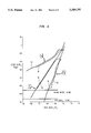
- FIG. 7 is a graph of the cuber circuit dynamic range as a function of bias current
- FIG. 8 shows graphs which compare predicted and measured results for a cuber circuit of the present invention
- FIG. 9 is an embodiment of a UHF cuber circuit according to the present invention.
- FIG. 10 shows graphs which compare predicted and measured results for a UHF cuber circuit
- FIG. 11 depicts an alternate embodiment of a low distortion amplifier circuit of the present invention.
- circuit 10 there is shown a predistortion power amplifier circuit 10 according to one embodiment of the present invention.
- circuit 10 will be described hereafter in reference to the low distortion amplification of a two tone input signal S in with high frequency, sinusoidal tones at frequencies f1 and f2. It is understood, however, that low distortion amplification of multi-tone input signals having more than two tones can also be accomplished with amplifier circuit 10.
- Amplifier circuit 10 includes power amplifier 20 functioning to produce high RF power at fundamental frequencies f1 and f2, which may lie in the UHF frequency band, for example.
- Frequencies f1 and f2 are assumed to be at fc- ⁇ and fc+ ⁇ , respectively, where fc is a reference carrier frequency.
- IMD intermodulation distortion
- these intermodulation products are substantially reduced by employing cuber circuit 14, which produces an optimum amount of power at distortion frequencies f3 and f4. This power will essentially cancel the power at f3 and f4 inherently produced by power amplifier 20 to produce a distortion free output signal S out .
- input signal S in is split by means of coupler 12 to produce a direct path output signal that is applied to delay line 13, and a coupled path output applied to cuber 14.
- Cuber 14 produces output signal S1 containing components at frequencies f1-f4 with the amplitude of each frequency component optimized.
- a highly linear, variable low noise amplifier (LNA) 16 amplifies signal S1 to adjust the amplitude of the cuber output.
- LNA variable low noise amplifier
- Variable phase shifter 17 is utilized to phase shift the output of LNA 16 to provide signal S2 that is applied to one input port of summer 18.
- the output of delay line 13 is applied to the other input port of summer 18.
- the primary function of delay line 13 is to match the delay, at frequencies f1 and f2, of the components in the predistortion path--that is, cuber 14, LNA 16 and interconnecting transmission lines (but not the desired phase shift of phase shifter 17).
- summer output signal S3 can be provided with the phase of the fundamental and distortion frequencies independently controlled.
- the f1 and 12 components of signal S3 will be the delay line 13 output signal minus signal S2, at an arbitrary phase of ⁇ f degrees.
- the f3 and f4 components of signal S2 will be at an arbitrary phase of ⁇ d degrees. If the delay line 13 electrical length changes, the magnitude of the f1 and f2 components of signal S3 will be increased because a pure subtraction no longer occurs and the phase will differ from ⁇ f. Meanwhile, the phase of the f3 and f4 components of signal S3 remains at ⁇ d.
- the absolute phase of the f1 and f2 components of signal S3 may be independently controlled relative to the absolute phase of the f3 and f4 components of signal S3.
- This independent phase control will enable cancellation of the distortion frequencies within power amplifier 20, provided that the amplitude of the distortion components of signal S3 is properly set. Accordingly, the AM to PM conversion in the amplifier 20 can be compensated for. For instance, if amplifier 20 has a voltage gain of G1 and the f3 and f4 components of signal S3 are each of a magnitude A3, then these components will be amplified and appear as components of the S out signal, each with amplitudes of A3G1.
- the f1 and f2 components of signal S3 are amplified and produce, as part of the S out signal, IMD products at f3 and f4, each with amplitude B3.
- the present embodiment is operative to provide this desirable result.
- This fifth order distortion consists of three parts: 1) the original fifth order distortion created by power amplifier 20 due only to the amplification of the f1 and f2 components of signal S3; 2) fifth order components of signal S2 due to imperfections in cuber circuit 14; and 3) fifth order distortion produced in power amplifier 20 due to the interaction between the f1, f2 components and f3, f4 components of the S3 signal as they are amplified. Since power amplifier 20 will operate in a more linear region than cuber circuit 14, item (2) above would be the dominant part among the 5th order terms. It is therefore important for the cuber to produce minimal 5th order residue.
- the cubic response of cuber circuit 14--i.e., the ability to produce third order intermodulation power (at frequencies fc+3 ⁇ and fc-3 ⁇ )--- is derived from the non-linear response of semiconductor diodes employed therein.
- each diode D1,D2 has the following voltage-current relationship:
- v is the voltage across the diode
- ⁇ is typically 40 volts -1
- I 0 is the reverse saturation current of each diode
- the combined current flow of the identical antiparallel diodes is,
- an output voltage can be obtained which consists of first, third and fifth order terms of the input voltage.
- the first order term can be cancelled by proper combining with the input voltage.
- the 5th order term can be made arbitrarily small by controlling the value of ⁇ v to be much less than unity. What remains, then, is essentially a 3rd order term.
- a typical high frequency diode has an I 0 current of about 20 nA, which implies a high conversion loss between the input and output signals. Therefore, thermal noise would overwhelm the output power, unless the circuit is operated at a large ⁇ v value; however, the latter would cause the higher order distortions to dominate the cubic distortion. Secondly, to avoid excessive conversion loss, a larger resistor is needed for the output voltage. It is noted that a large resistor in circuit 22 would change the ideal voltage-current formula of equation (2).
- a pair of packaged diodes D3 and D4 include ideal diodes D1 and D2, respectively, with each ideal diode in series with a bulk resistance R b .
- This bulk resistance R b is associated with every commercially available diode and is typically on the order of 10-20 ohms.
- a pair of DC sources 30 each supply a DC bias voltage V b in a series path with each diode D3 and D4. The introduction of bias voltage V b produces a bias current, I b , which is many orders of magnitude larger than I 0 .
- the current I b is added with the currents i1 and i2 that would otherwise flow through respective ideal diodes D1 and D2, so that the current i1+I b now flows through diode D3, and current i 2 +I b flows through diode D4.
- Replacing voltage source 24 of the ideal circuit of FIG. 2 is the series combination of a voltage source 26 that produces a time varying input voltage V i , a source impedance R s and a load impedance R L .
- Load impedance R L is essentially the input impedance of amplifier 16 of FIG. 1. If an impedance transformer is utilized between cuber circuit 14 and amplifier 16, R L will be the impedance "looking into” the transformer/amplifier arrangement. Load resistance R L is introduced to derive meaningful power to combat subsequent amplifier noise.
- the voltage V i represents the superimposed, multi-tone sinusoidal voltages supplied to cuber 14 from the coupled output path of coupler 12.
- Source impedance R s is the impedance "looking back" towards directional coupler 12 from cuber input port 15.
- characteristic impedance Zo of coupler 12 is 50 ⁇ ; however it is desirable to transform the 50 ⁇ impedance to a much lower impedance on the order of one ohm.
- impedance R s will be the lower transformed impedance.
- the transformation may be realized at higher frequencies with the use of a multi-stepped microstrip transformer (not shown) between coupler 12 and cuber circuit 14 with each step being a quarter wavelength long so that the 50 ⁇ impedance is transformed in several steps down to the much lower impedance R s .
- Such multi-stepped transformers are well known in the art and generally utilized to transform impedances over narrow to medium range bandwidths. At lower frequencies, a lumped element transformer would be used.
- This embodiment uses optimized values for the parameters R b , R s , R L , and V b , which are selected to arrive at cuber circuit 14, which can operate over an optimized dynamic range of V i .
- the mathematical power series based analysis set forth below enables one skilled in the art to select the above-noted parameters so that a desired cuber circuit output power at the third order frequencies is obtained while output power at fifth and higher order frequencies is minimized.
- the lower end of the dynamic range will be shown to be limited by the noise within the circuit; the higher end is limited by the eventual dominance of the fifth and higher order power over the third order power.
- a voltage V d1 will appear across the diode D1 as:
- Equation (8) can first be solved for V as a power series expansion in i 1 /I s : ##EQU3## where ⁇ is defined as:
- Equation (12) the desired power series of i in terms of V i , Equation (12), where the coefficients are given by: ##EQU9## It is noted that, for a given bias voltage V b , the output voltage across R L is completely defined by iR L , where i is given by ##EQU10## and the C's are defined by Equations (21)-(24). It is also noted that C 5 , i.e., the 5th order distortion, can be reduced by adjusting R, for any fixed bias current.
- a convenient method of measuring the performance of cuber circuit 14 is to use a time varying input voltage V i consisting of two sine waves of different frequencies fc+ ⁇ and fc- ⁇ as mentioned previously. It is understood, however, that cuber circuit 14 can also be used to generate third order output when V i is made up of more than two sinusoidal tones. (Moreover, it is noted that cuber circuit 14 can also be used to generate third harmonic power for a single tone input, to cancel or tailor third harmonic power generated in the main power amplifier. This would be desirable in some microwave amplifiers to increase efficiency by shaping voltage and current waveforms using harmonic power.)
- V i is defined as:
- Equation (12) Inserting Equation (25) into Equation (12) and retaining only terms in the band centered on the radian carrier frequency, ⁇ c , a current i f flowing through R L in the fundamental frequency band, can be found as: ##EQU11##
- cuber circuit 14 Since the purpose of cuber circuit 14 is to provide a third order output that can be used to cancel the third order power generated in power amplifier 20, the fifth and higher order distortion from cuber 14 are undesirable, unless they can be controlled to cancel similar terms in the power amplifier. Thus, for example, if it is desired to cancel the third order distortion by 30 dB, the high power limit of the cuber predistorter arrangement occurs when the input power to cuber 14 is high enough to make the fifth and higher order distortion equal to 0.1% (i.e., -30 dB) of the third order output of the cuber. Allowing the input power to rise above this point would begin to defeat the purpose of the cuber circuit arrangement of canceling third order distortion output, since higher order distortion output would begin to rise to unacceptably higher levels.
- a simple way to ensure dominance of the third order relative to the higher order distortion is to attenuate the input signal to cuber 14 and amplify its output using variable amplifier 16 before coupling to the input of power amplifier 20.
- the difficulty with this approach is that the third order cuber output becomes comparable to its noise output.
- the dynamic range of cuber 14 is determined by the range of input power between the lowest input power level--that is, the level where its third order output power is comparable to its noise output--and the highest input power level, which is where the higher order distortion becomes comparable to the third order output.
- An important parameter in estimating the cuber noise output is its bandwidth. For example, in wireless communication applications, it is desirable to cancel the intermodulation in a radio channel to be 60 dB below the carrier level that is normally used for radio transmission in that channel (-60 dBc). At the low power limit of operation, the intermodulation of the power amplifier should just be rising above the -60 dBc level, so it would be desirable for the noise in the channel bandwidth to be about 10 dB less (-70 dBc). To compare this with the third order output of cuber 14, it is necessary to specify the number of channels, M, transmitted. The third order output per channel is approximately 1/Mth of the total intermodulation output.
- the low power end of the dynamic range of cuber 14 is the point where the noise power output per channel bandwidth is about 10 Log 10 (10M) dB below the third order output. Since the upper limit of the dynamic range is roughly independent of the number of channels, it is seen that the dynamic range is reduced as the number of channels increases.
- the noise sources of cuber 14 consist of shot noise I shot-1 , I shot-2 in the respective diodes D1, D2; the resistor thermal noises e Rb , e RS ; and the noise introduced by low noise amplifier 16.
- the effective resistance of the diode junctions are biased, by means of D.C. sources 30, to be much larger than resistances R s , R b and R L .
- the load resistance R L in FIG. 4 is shown to consist of the impedance looking into a transformer 34 in front of the LNA 16.
- the mean square shot noise current of a diode is given by:
- the noise of amplifier 16 is represented by equivalent input noise voltage e na and current I na generators which can typically be assumed to be uncorrelated. The ratio of their magnitude is called the noise resistance, R n .tbd. e .sbsp.na / i .sbsb.na.
- the noise resistance R n of amplifier 16 can be measured by comparing its output noise when the amplifier input is open circuited, "N oc " to that when the amplifier input is short circuited, “N sc ", as follows: ##EQU12## Then, in terms of amplifier 16 noise figure, F, e 2 na is defined as ##EQU13## Typically, N oc >>N sc , so that the amplifier equivalent input noise current I na dominates over its equivalent input noise voltage e na and R n is small compared to unity.
- Equation (26) The mean square noise current through R L due to e na is, using the same approximation for C 1 as in Equation (28), ##EQU14## As in Equation (26), it is assumed that the small signal junction resistance of the diodes is large compared to R L , so that most of i na flows through R L : ##EQU15## The total mean square noise current i 2 nt through R L is thus the sum of that given in Equations (28)-(30), and (32)-(34), ##EQU16## It will be shown in later examples that the equivalent input noise current of LNA 16 is the dominant noise source so that the total mean square noise current may usually be approximated by
- LNA 16 Since LNA 16 is usually needed to set the level of the third order predistortion to be coupled into the input of power amplifier 20, it cannot be deleted in most practical applications to avoid the major noise source.
- the cuber output signal flowing through R L is the third order current i S3 in Eqn. (12), that is: ##EQU17## where A(t) and ⁇ (t) are the slowly varying (with respect to the radian carrier frequency, ⁇ c ) envelope and phase, respectively, of the narrowband representation of the input signal.
- X is the power amplifier intermodulation level, relative to the channel bandwidth noise level--e.g., 10 dB in the above example.
- V imin to cuber circuit 14 guidelines for determining a maximum input voltage, V imax will now be presented. A determination of V imax will then establish the dynamic range of cuber circuit 14.
- V imin is defined as the input voltage which yields a 3rd order output mean square current which is X times stronger than the mean square noise current (primarily the output amplifier 16 noise) on a per-channel basis.
- X 10 as an illustrative case
- Eqns. (35), (38) and (39) give, ##EQU19##
- V imax The maximum cuber circuit input voltage, V imax , is defined hereafter as the input voltage which produces 5th or 7th order output voltages that are within "Y" dB of the 3rd order output, where Y represent the amount of 3rd order power cancellation which is desired in power amplifier 20.
- An exemplary value for Y is 30 dB (or 1,000).
- the decibel difference between V imax and V imin is defined as the dynamic range: 20 Log 10 (V imax )/V imin ).
- V imax is in the range of 2 to 3, or V imax is about 50 to 75 mV--a result which is fairly independent of the bias current or the total resistance in the circuit.
- a diode resistance R D is conveniently defined by ##EQU21##
- Plotting dynamic range versus (R L +R s +R b )/R D shows the similarity in the dynamic range dependence on resistance for various bias currents.
- the optimum total resistance R L +R s +R b which produces maximum dynamic range, is about 11% of R D , roughly independent of the bias current. Indeed, if one neglects higher powers of ⁇ IsR, the resistance which nulls the fifth order output satisfies ##EQU22## which approximates the 11% result. With the fifth order output nulled, V imax is seen to be dependent primarily on ⁇ , under the approximation: ##EQU23##
- V out (which is an amplified replica of the cuber circuit 14 output) of the various orders of nonlinearity are shown as a function of the cuber circuit input voltage, V i .
- Graphs 40, 41 and 42 (to be read with the left hand vertical axis) are plots of the fundamental components V 0 and third order components V 3 , respectively, of V out , versus V i ;
- graph 42 shows the relationship (V 0 -V i C 1 ) versus V i .
- the near optimum bias of 20 ⁇ A is about 10,000 times larger than the 2 nA I 0 and provides about 40 dB more noise margin to the cuber output compared to the non-biased case.
- FIG. 7 there is shown a graph 48 representing optimized dynamic range as a function of bias current I s .
- the dynamic range peaks at a value of 17.9 dB for a bias current of 50 ⁇ A.
- Further reduction of R D through biasing changes the exponential nature of the diode I-V curve toward linear and therefore reduces the non-linearity of the diode pair. Less non-linearity implies a smaller C 3 component and thus a smaller output noise margin.
- FIG. 8 there is shown measured (dotted lines) versus predicted (solid lines) results for cuber circuit 14 of FIG. 3.
- the results are for the two-tone input signal case, and with LNA 16 input impedance as the load impedance R L .
- the diode junction capacitance is 0.6 pF, and transit time is 6 nanoseconds.
- curve 52 represents the predicted fundamental component voltage V 0 , per tone, of the LNA output voltage V out , as a function of the input voltage V i to tuber circuit 14 with the circuit parameters as described above, and using the power series approximation described previously.
- Curve 53 represents the corresponding measured results for V 0 .
- curves 54 and 55 are the predicted and measured results, respectively, for the third order component V 3 , per tone, of LNA 16 output voltage; curves 56 and 57 are the respective predicted and measured fifth order voltage V 5 . From the figure it is seen that the power series approximation is accurate until ⁇ V exceeds unity.
- FIG. 9 shows a cuber circuit 80 suitable for use at UHF frequencies which can be used for cuber circuit 14 of FIG. 1.
- the equations (4)-(46) governing the performance of cuber circuit 14, are equally applicable to cuber circuit 80, with the following subtleties.
- the aforementioned load impedance R L is comprised of a shunt resistance R p in parallel with input impedance R L ' of LNA 16.
- voltage sources 30 of FIG. 4 which produce the bias voltages V b , are realized by capacitors C1 and C2, each of which stores a bias voltage V b .
- the driving force behind this biasing is a variable voltage source 88 that produces a bias voltage of 2 V b .
- AC chokes 82 and 84 preferably inductors with ferrite beads to prevent the bias circuit from loading down the RF signals, are employed to introduce the DC bias to the anti-parallel diode configuration, thereby allowing bias current I b to flow.
- Capacitor C3 acts as a D.C. block. This biasing arrangement is more practical than one which utilizes a separate D.C. source in series with diodes D3 and D4, as was depicted in FIG. 3--yet the same biasing function is realized with the single source approach.
- the components within the dotted line 86 comprise the printed circuit portion of the cuber circuit.
- the antiparallel diodes inside dotted line 87 are available as a commercial package from Hewlett Packard, HP part #2812. This part is typically utilized in mixer applications where D.C. bias is not used to bias the diodes D3 and D4.
- Cuber circuit 80 was built using the above-noted HP anti-parallel diode package and tested at 900 MHz.
- Dotted lines 91, 93 and 95 are the measured results for the V 0 , V 3 and V 5 components of the output voltage whereas solid lines 92, 94 and 96 represent the predicted results using the above described power series approximation for V 0 , V 3 and V 5 , respectively.
- the shown power series curves are generated with a low frequency approximation, which does not include the effects of diode transit time or capacitance.
- the main effect of operating at UHF is that much of the diode current is shunted by capacitance.
- the diode capacitance allows about 15 dB more fundamental signal leak-through than for the low frequency case. This much leak through causes the cuber 80 to have a significant effect on the net gain of the power amplifier 20 of FIG. 1 where it is used for cubic distortion cancellation (typically about 4 to 5 dB).
- a small preamplifier (not shown) in the direct path between summer 18 and amplifier 20, it is possible to correct this effect with negligible effect on efficiency, distortion, or dynamic range.
- the correction circuitry is operable to detect IMD energy within output signal S out and to provide a control signal V co to LNA 16 to control its gain in accordance with the IMD energy detected.
- LNA 16 gain is continuously adjusted to control the third order power level of signal S3 so that the IMD power of S out is always kept at a minimum level.
- Continuous correction for maximum IMD cancellation is accomplished by first coupling signal energy or signal S out with directional coupler 61 towards down-converter 62.
- Local oscillator 64 which is preferably a comb frequency local oscillator, provides an L.O. signal to down converter 62 so that the coupled RF signal is down converted to an intermediate frequency (IF) that is applied to narrow band pass filter (BPF) 65.
- filter 65 having a resonant frequency at one of the third order IMD frequencies fc+3 ⁇ or fc-3 ⁇ (down-converted), only the third order distortion power, and not the fundamental power at fc+ ⁇ and fc- ⁇ , passes through filter 65 and is detected by diode detector 67. Detector 67 then produces an error voltage "V err " indicative of the unwanted IMD power, which is applied to multiplier 68.
- down-converter 62 in conjunction with the local oscillator 64 is preferable to allow for the use of a low cost, narrow band pass filter 65, it is understood that these components could be eliminated if filter 65 is designed with a resonant frequency at the higher RF frequencies of fc+3 ⁇ or fc-3 ⁇ . Since narrower filters are generally available at lower IF frequencies, the former approach is, of course, preferable.
- Dither generator 66 generates a continuous sequence of voltage pulses, which may be a square wave pulse train. This voltage pulse sequence is applied to multiplier 68 and also to an input port of summer circuit 73. Multiplier 68 multiplies the instantaneous voltage level of the voltage pulse sequence with that of error signal V err , to produce a multiplied output signal that is supplied to integrator 72. Integrator 72 then integrates the multiplied output signal over time to provide an integrated output that is supplied to the other input of summer circuit 73. The dither generator voltage pulse sequence is then summed with the integrator output by summer circuit 73 to produce the control voltage V co which controls LNA 16 gain, preferably by controlling the bias voltage therein.
- each voltage pulse of the sequence will produce an instantaneous change in the error voltage V err .
- the change in V err is correlated with the voltage pulse that produced the change.
- the integrator output voltage will slowly converge to the point at which V err , and hence the undesired IMD energy, is reduced below a minimum threshold.
- the continuously corrected low distortion amplifier circuit 70 is particularly useful in wireless communications base stations where the used channels are sparsely spaced with respect to frequency.
- the filtering by BPF 65 is advantageously performed in the unused channels, where only the intermodulation products appear.
- control techniques may be utilized to continuously vary the control voltage V co until the error voltage V err is indicative of minimum intermodulation power in the output signal.
- the controlling circuit configuration encompassing dither generator 66, multiplier 68, integrator 72 and summer 73, may be replaced by a microprocessor in conjunction with a sample and hold circuit, A/D and D/A converters, whereby the detected error signal would be sampled and the control voltage V co adjusted in accordance therewith.
- the microprocessor would be used to control incrementing and decrementing of the voltage V co until it is optimized.
Abstract
Description
i.sub.D =I.sub.0 (e.sup.βv -1), (1)
i=i.sub.1 -i.sub.2 =I.sub.0 (e.sup.βv -e.sup.-βv).(2)
V=V.sub.i -iR, (4)
I.sub.b =I.sub.0 (e.sup.β(v.sbsp.b.sup.-I.sbsp.b.sup.R.sbsp.b.sup.) -1). (5)
V.sub.d1 =V-i.sub.1 R.sub.b +V.sub.b -I.sub.b R.sub.b. (6)
i.sub.1 +I.sub.b =I.sub.0 (e.sup.βV.sbsp.d1 -1)=(I.sub.b +I.sub.0)e.sup.β(V-i.sbsp.1.sup.R.sbsp.b.sup.) -I.sub.0,(7)
i.sub.1 =I.sub.s e.sup.β(V-i.sbsp.1.sup.R.sbsp.b.sup.) -I.sub.s,(8)
i.sub.2 =I.sub.s e.sup.-β(V+i.sbsp.2.sup.R.sbsp.b.sup.) -I.sub.s,(9)
i=i.sub.1 -i.sub.2 =I.sub.s [e.sup.β(V-i.sbsp.1.sup.R.sbsp.b.sup.) -e.sup.-β(V+i.sbsp.2.sup.R.sbsp.b.sup.) ]. (10)
i(V)=-i(-V) and i(V.sub.i)=-i(-V.sub.i). (11)
ξ.tbd.1+I.sub.s βR.sub.b. (14)
η.tbd.1+I.sub.s β(R.sub.b +2R). (20)
V.sub.i =acos (ω.sub.c t+δt)+acos (ω.sub.c t-δt)=2 acos (δt) cos (ω.sub.c t), (25)
I.sup.2.sub.shot =2qIB, (27)
i.sup.2.sub.shot ≅4qI.sub.b B, (28)
i.sup.2.sub.nb ≅8kTBR.sub.b (βI.sub.s).sup.2,(29)
i.sup.2.sub.ns ≅(2βI.sub.s).sup.2 4kTBR.sub.s.(30)
i.sup.2.sub.nt ≅4kTB(F-1)R.sub.L. (36)
i.sup.2.sub.S3 ≅XMi.sup.2.sub.nt, (39)
Claims (20)
(C7/7!).sup.2 Vimax.sup.14 +(C5/5!).sup.2 Vimax.sup.10 =(C3/3!).sup.2 Vimax.sup.6 /Y,
i=C1Vi+(C3/3!)Vi.sup.3 +(C5/5!)Vi.sup.5 +(C7/7!)Vi.sup.7 +. . .
Priority Applications (3)
| Application Number | Priority Date | Filing Date | Title |
|---|---|---|---|
| US08/534,371 US5589797A (en) | 1995-09-26 | 1995-09-26 | Low distortion amplifier |
| EP96306730A EP0766378A3 (en) | 1995-09-26 | 1996-09-17 | Low distortion amplifier |
| JP8254061A JPH09135123A (en) | 1995-09-26 | 1996-09-26 | Low-distortion amplifier |
Applications Claiming Priority (1)
| Application Number | Priority Date | Filing Date | Title |
|---|---|---|---|
| US08/534,371 US5589797A (en) | 1995-09-26 | 1995-09-26 | Low distortion amplifier |
Publications (1)
| Publication Number | Publication Date |
|---|---|
| US5589797A true US5589797A (en) | 1996-12-31 |
Family
ID=24129760
Family Applications (1)
| Application Number | Title | Priority Date | Filing Date |
|---|---|---|---|
| US08/534,371 Expired - Lifetime US5589797A (en) | 1995-09-26 | 1995-09-26 | Low distortion amplifier |
Country Status (3)
| Country | Link |
|---|---|
| US (1) | US5589797A (en) |
| EP (1) | EP0766378A3 (en) |
| JP (1) | JPH09135123A (en) |
Cited By (44)
| Publication number | Priority date | Publication date | Assignee | Title |
|---|---|---|---|---|
| US5798854A (en) * | 1994-05-19 | 1998-08-25 | Ortel Corporation | In-line predistorter for linearization of electronic and optical signals |
| US5909642A (en) * | 1996-07-05 | 1999-06-01 | Fujitsu Limited | Nonlinear distortion detecting circuit and nonlinear distortion compensating circuit for transmitter |
| WO2000005591A1 (en) * | 1998-07-21 | 2000-02-03 | Ifr Limited | Method of and apparatus for generating a multitone test signal |
| US6038460A (en) * | 1997-06-18 | 2000-03-14 | Lucent Technologies Inc. | Receiver for an RF signal booster in wireless communication system |
| US6055278A (en) * | 1996-04-26 | 2000-04-25 | C-Cor.Net Corporation | Linearization circuits and methods |
| US6140858A (en) * | 1996-03-20 | 2000-10-31 | U.S. Philips Corporation | Predistortion circuit for an analog signal in a video communication network |
| US6253070B1 (en) * | 1998-07-22 | 2001-06-26 | Denso Corporation | Diode amplifier bypass circuit |
| WO2001054268A2 (en) * | 2000-01-24 | 2001-07-26 | General Instrument Corporation | Circuit for reducing second and third order intermodulation distortion for a broadband rf amplifier |
| US6288814B1 (en) | 1994-05-19 | 2001-09-11 | Ortel Corporation | In-line predistorter for linearization of electronic and optical signals |
| US6388526B1 (en) * | 2000-07-06 | 2002-05-14 | Lucent Technologies Inc. | Methods and apparatus for high performance reception of radio frequency communication signals |
| US6404284B1 (en) * | 2001-04-19 | 2002-06-11 | Anadigics, Inc. | Amplifier bias adjustment circuit to maintain high-output third-order intermodulation distortion performance |
| US6466084B1 (en) | 2000-01-24 | 2002-10-15 | General Instrument Corporation | Circuit for reducing third order intermodulation distortion for a broadband RF amplifier |
| US6570430B1 (en) | 1999-04-01 | 2003-05-27 | General Instrument Corporation | Non-linear distortion generator for both second and third order distortion |
| US20030102911A1 (en) * | 2001-11-30 | 2003-06-05 | Gopal Raghavan | Bipolar transistor-based linearizer with programmable gain and phase response system |
| US6577177B2 (en) | 1999-04-01 | 2003-06-10 | General Instrument Corporation | Non-linear distortion generator |
| US6587243B1 (en) * | 1999-12-10 | 2003-07-01 | General Instrument Corporation | Second order predistortor for a return laser transmitter |
| US20030161487A1 (en) * | 2002-02-28 | 2003-08-28 | Husted Paul J. | Method and apparatus for transient frequency distortion compensation |
| US6624695B2 (en) * | 2001-10-31 | 2003-09-23 | Tropian, Inc. | Waveform pershaping for efficiency improvements in DC to RF conversion |
| US20040008083A1 (en) * | 2002-07-09 | 2004-01-15 | General Instrument Corporation | Inline predistortion for both CSO and CTB correction |
| US6700439B2 (en) | 2002-04-11 | 2004-03-02 | Andrew Corporation | Zero-bias bypass switch |
| US20040052536A1 (en) * | 2002-09-17 | 2004-03-18 | General Instrument Corporation | Second order predistortion circuit |
| US20040125885A1 (en) * | 2002-12-27 | 2004-07-01 | Roger Branson | Intermodulation product cancellation in communications |
| US20040127183A1 (en) * | 2002-12-27 | 2004-07-01 | Roger Branson | Intermodulation product cancellation in communications |
| US6766158B1 (en) * | 2001-03-30 | 2004-07-20 | Skyworks Solutions, Inc. | Harmonic cancellation mixer |
| US6794937B1 (en) * | 2001-11-30 | 2004-09-21 | Alcatel | Predistortion linearizer and method for linearizing a nonlinear device |
| US20040198465A1 (en) * | 2002-10-03 | 2004-10-07 | Nation Med A. | Portable communication device having adjustable amplification and method therefor |
| US6812786B2 (en) | 2002-04-11 | 2004-11-02 | Andrew Corporation | Zero-bias bypass switching circuit using mismatched 90 degrees hybrid |
| US20050195030A1 (en) * | 2004-01-29 | 2005-09-08 | Takashi Okazaki | Predistorter |
| US20060046665A1 (en) * | 2002-05-01 | 2006-03-02 | Dali Yang | System and method for digital memorized predistortion for wireless communication |
| US20070098417A1 (en) * | 2005-10-27 | 2007-05-03 | Eva Peral | Distortion cancellation circuitry for optical receivers |
| US20070297803A1 (en) * | 2006-06-21 | 2007-12-27 | Eva Peral | In-line distortion cancellation circuits for linearization of electronic and optical signals with phase and frequency adjustment |
| US7385447B1 (en) | 2004-06-28 | 2008-06-10 | Anadigics, Inc. | Power amplifier having curve-fitting predistorter |
| US7508266B1 (en) | 2006-08-29 | 2009-03-24 | Pmc-Sierra, Inc. | Method for enhancing linearity of a transistor amplifier using switched capacitive loads |
| US20090091487A1 (en) * | 2007-10-04 | 2009-04-09 | Texas Instruments Incorporated | Spurious Free Dynamic Range Of An Analog To Digital Converter |
| US20100141339A1 (en) * | 2008-10-17 | 2010-06-10 | Day Chris J | Apparatus and Method for Broadband Amplifier Linearization |
| US8472897B1 (en) | 2006-12-22 | 2013-06-25 | Dali Systems Co. Ltd. | Power amplifier predistortion methods and apparatus |
| US8620234B2 (en) | 2002-05-01 | 2013-12-31 | Dali Systems Co., Ltd. | High efficiency linearization power amplifier for wireless communication |
| US20140300401A1 (en) * | 2013-04-05 | 2014-10-09 | Joshua D. Kaggie | Methods of Circuit Construction to Improve Diode Performance |
| US9077297B2 (en) | 2002-05-01 | 2015-07-07 | Dali Systems Co., Ltd. | Power amplifier time-delay invariant predistortion methods and apparatus |
| US9331633B1 (en) * | 2013-03-15 | 2016-05-03 | Anritsu Company | System and method for eliminating intermodulation |
| WO2016179541A1 (en) * | 2015-05-06 | 2016-11-10 | Rfaxis, Inc. | Rf power amplifiers with diode linearizer |
| US11129076B2 (en) | 2006-12-26 | 2021-09-21 | Dali Wireless, Inc. | Method and system for baseband predistortion linearization in multi-channel wideband communication systems |
| US11418155B2 (en) | 2002-05-01 | 2022-08-16 | Dali Wireless, Inc. | Digital hybrid mode power amplifier system |
| US20220295487A1 (en) | 2010-09-14 | 2022-09-15 | Dali Wireless, Inc. | Remotely reconfigurable distributed antenna system and methods |
Citations (3)
| Publication number | Priority date | Publication date | Assignee | Title |
|---|---|---|---|---|
| US4157508A (en) * | 1977-11-21 | 1979-06-05 | Bell Telephone Laboratories, Incorporated | Signal cuber circuit |
| US4513250A (en) * | 1983-05-31 | 1985-04-23 | Northern Telecom Limited | Signal cuber |
| US4943783A (en) * | 1989-07-31 | 1990-07-24 | Nippon Telegraph And Telephone Corporation | Feed forward distortion correction circuit |
Family Cites Families (3)
| Publication number | Priority date | Publication date | Assignee | Title |
|---|---|---|---|---|
| JPS50140040A (en) * | 1974-04-25 | 1975-11-10 | ||
| DE3024533A1 (en) * | 1980-06-28 | 1982-01-21 | Robert Bosch Gmbh, 7000 Stuttgart | Compensating circuit for intermodulation interference of VHF signal - interference signal being filtered out by anti-parallel diodes and inverted, esp. for third order interference |
| CA1190607A (en) * | 1983-05-31 | 1985-07-16 | Stephen G. Harman | Signal cuber |
-
1995
- 1995-09-26 US US08/534,371 patent/US5589797A/en not_active Expired - Lifetime
-
1996
- 1996-09-17 EP EP96306730A patent/EP0766378A3/en not_active Withdrawn
- 1996-09-26 JP JP8254061A patent/JPH09135123A/en active Pending
Patent Citations (3)
| Publication number | Priority date | Publication date | Assignee | Title |
|---|---|---|---|---|
| US4157508A (en) * | 1977-11-21 | 1979-06-05 | Bell Telephone Laboratories, Incorporated | Signal cuber circuit |
| US4513250A (en) * | 1983-05-31 | 1985-04-23 | Northern Telecom Limited | Signal cuber |
| US4943783A (en) * | 1989-07-31 | 1990-07-24 | Nippon Telegraph And Telephone Corporation | Feed forward distortion correction circuit |
Non-Patent Citations (6)
| Title |
|---|
| M. Abramowitz and I. A. Stegun, Eds., "Handbook of Mathematical Functions", National Bureau of Standards, Applied Mathematics Series #55, 3rd Printing, Mar. 1965, p. 16, Eq. (3.6.25). |
| M. Abramowitz and I. A. Stegun, Eds., Handbook of Mathematical Functions , National Bureau of Standards, Applied Mathematics Series 55, 3rd Printing, Mar. 1965, p. 16, Eq. (3.6.25). * |
| R. J. Westcott, "Investigation of multiple f.m./f.d.m. carriers through a satellite t.w.t. operating near to saturation", IEE. vol. 114, No. 6, Jun. 1967, pp. 726-740. |
| R. J. Westcott, Investigation of multiple f.m./f.d.m. carriers through a satellite t.w.t. operating near to saturation , IEE. vol. 114, No. 6, Jun. 1967, pp. 726 740. * |
| T. Nojima and T. Konno, "Cuber Predistortion Linearizer for Relay Equipment in 800 MHz Band Land Mobile Telehone System", IEEE Transactions on Vehicular Technology, vol. VT-34, No. 4, Nov., 1985, pp. 169-177. |
| T. Nojima and T. Konno, Cuber Predistortion Linearizer for Relay Equipment in 800 MHz Band Land Mobile Telehone System , IEEE Transactions on Vehicular Technology, vol. VT 34, No. 4, Nov., 1985, pp. 169 177. * |
Cited By (82)
| Publication number | Priority date | Publication date | Assignee | Title |
|---|---|---|---|---|
| US5798854A (en) * | 1994-05-19 | 1998-08-25 | Ortel Corporation | In-line predistorter for linearization of electronic and optical signals |
| US6288814B1 (en) | 1994-05-19 | 2001-09-11 | Ortel Corporation | In-line predistorter for linearization of electronic and optical signals |
| US6140858A (en) * | 1996-03-20 | 2000-10-31 | U.S. Philips Corporation | Predistortion circuit for an analog signal in a video communication network |
| US6055278A (en) * | 1996-04-26 | 2000-04-25 | C-Cor.Net Corporation | Linearization circuits and methods |
| US5909642A (en) * | 1996-07-05 | 1999-06-01 | Fujitsu Limited | Nonlinear distortion detecting circuit and nonlinear distortion compensating circuit for transmitter |
| US6038460A (en) * | 1997-06-18 | 2000-03-14 | Lucent Technologies Inc. | Receiver for an RF signal booster in wireless communication system |
| WO2000005591A1 (en) * | 1998-07-21 | 2000-02-03 | Ifr Limited | Method of and apparatus for generating a multitone test signal |
| GB2339917A (en) * | 1998-07-21 | 2000-02-09 | Ifr Limited | Generating a multitone test signal |
| US6253070B1 (en) * | 1998-07-22 | 2001-06-26 | Denso Corporation | Diode amplifier bypass circuit |
| US6570430B1 (en) | 1999-04-01 | 2003-05-27 | General Instrument Corporation | Non-linear distortion generator for both second and third order distortion |
| US6577177B2 (en) | 1999-04-01 | 2003-06-10 | General Instrument Corporation | Non-linear distortion generator |
| US6587243B1 (en) * | 1999-12-10 | 2003-07-01 | General Instrument Corporation | Second order predistortor for a return laser transmitter |
| US6759897B2 (en) | 2000-01-24 | 2004-07-06 | General Instrument Corporation | Circuit for reducing second and third order intermodulation distortion for a broadband RF amplifier |
| WO2001054268A2 (en) * | 2000-01-24 | 2001-07-26 | General Instrument Corporation | Circuit for reducing second and third order intermodulation distortion for a broadband rf amplifier |
| US6509789B1 (en) | 2000-01-24 | 2003-01-21 | General Instrument Corporation | Circuit for reducing second and third order intermodulation distortion for a broadband RF amplifier |
| WO2001054268A3 (en) * | 2000-01-24 | 2002-02-07 | Gen Instrument Corp | Circuit for reducing second and third order intermodulation distortion for a broadband rf amplifier |
| US6466084B1 (en) | 2000-01-24 | 2002-10-15 | General Instrument Corporation | Circuit for reducing third order intermodulation distortion for a broadband RF amplifier |
| US6388526B1 (en) * | 2000-07-06 | 2002-05-14 | Lucent Technologies Inc. | Methods and apparatus for high performance reception of radio frequency communication signals |
| US6766158B1 (en) * | 2001-03-30 | 2004-07-20 | Skyworks Solutions, Inc. | Harmonic cancellation mixer |
| US6639466B2 (en) | 2001-04-19 | 2003-10-28 | Anadigics Inc. | Amplifier bias adjustment circuit to maintain high-output third-order intermodulation distortion performance |
| US6404284B1 (en) * | 2001-04-19 | 2002-06-11 | Anadigics, Inc. | Amplifier bias adjustment circuit to maintain high-output third-order intermodulation distortion performance |
| US6624695B2 (en) * | 2001-10-31 | 2003-09-23 | Tropian, Inc. | Waveform pershaping for efficiency improvements in DC to RF conversion |
| US20030102911A1 (en) * | 2001-11-30 | 2003-06-05 | Gopal Raghavan | Bipolar transistor-based linearizer with programmable gain and phase response system |
| US6794937B1 (en) * | 2001-11-30 | 2004-09-21 | Alcatel | Predistortion linearizer and method for linearizing a nonlinear device |
| US6750709B2 (en) * | 2001-11-30 | 2004-06-15 | The Boeing Company | Bipolar transistor-based linearizer with programmable gain and phase response system |
| US20100222092A1 (en) * | 2002-02-28 | 2010-09-02 | Husted Paul J | Method And Apparatus For Transient Frequency Distortion Compensation |
| US8494568B2 (en) | 2002-02-28 | 2013-07-23 | Qualcomm Incorporated | Method and apparatus for transient frequency distortion compensation |
| US8346288B2 (en) | 2002-02-28 | 2013-01-01 | Qualcomm Incorporated | Method and apparatus for transient frequency distortion compensation |
| US8019369B2 (en) | 2002-02-28 | 2011-09-13 | Qualcomm Atheros, Inc. | Method and apparatus for transient frequency distortion compensation |
| US7742778B2 (en) | 2002-02-28 | 2010-06-22 | Atheros Communications, Inc. | Method and apparatus for transient frequency distortion compensation |
| WO2003075449A2 (en) * | 2002-02-28 | 2003-09-12 | Atheros Communications, Inc. | Method and apparatus for transient frequency distortion compensation |
| US20030161487A1 (en) * | 2002-02-28 | 2003-08-28 | Husted Paul J. | Method and apparatus for transient frequency distortion compensation |
| WO2003075449A3 (en) * | 2002-02-28 | 2003-12-11 | Atheros Comm Inc | Method and apparatus for transient frequency distortion compensation |
| US7340265B2 (en) | 2002-02-28 | 2008-03-04 | Atheros Communications, Inc. | Method and apparatus for transient frequency distortion compensation |
| US6700439B2 (en) | 2002-04-11 | 2004-03-02 | Andrew Corporation | Zero-bias bypass switch |
| US6812786B2 (en) | 2002-04-11 | 2004-11-02 | Andrew Corporation | Zero-bias bypass switching circuit using mismatched 90 degrees hybrid |
| US8620234B2 (en) | 2002-05-01 | 2013-12-31 | Dali Systems Co., Ltd. | High efficiency linearization power amplifier for wireless communication |
| US9742446B2 (en) | 2002-05-01 | 2017-08-22 | Dali Wireless, Inc. | High efficiency linearization power amplifier for wireless communication |
| US9054758B2 (en) | 2002-05-01 | 2015-06-09 | Dali Systems Co. Ltd. | High efficiency linearization power amplifier for wireless communication |
| US9077297B2 (en) | 2002-05-01 | 2015-07-07 | Dali Systems Co., Ltd. | Power amplifier time-delay invariant predistortion methods and apparatus |
| US11418155B2 (en) | 2002-05-01 | 2022-08-16 | Dali Wireless, Inc. | Digital hybrid mode power amplifier system |
| US8326238B2 (en) * | 2002-05-01 | 2012-12-04 | Dali Systems Co, Ltd. | System and method for digital memorized predistortion for wireless communication |
| US9374196B2 (en) | 2002-05-01 | 2016-06-21 | Dali Systems Co. Ltd. | System and method for digital memorized predistortion for wireless communication |
| US11159129B2 (en) | 2002-05-01 | 2021-10-26 | Dali Wireless, Inc. | Power amplifier time-delay invariant predistortion methods and apparatus |
| US9031521B2 (en) | 2002-05-01 | 2015-05-12 | Dali Systems Co. Ltd. | System and method for digital memorized predistortion for wireless communication |
| US10097142B2 (en) | 2002-05-01 | 2018-10-09 | Dali Wireless, Inc. | Power amplifier time-delay invariant predistortion methods and apparatus |
| US10985965B2 (en) | 2002-05-01 | 2021-04-20 | Dali Wireless, Inc. | System and method for digital memorized predistortion for wireless communication |
| US10693425B2 (en) | 2002-05-01 | 2020-06-23 | Dali Wireless, Inc. | Power amplifier time-delay invariant predistortion methods and apparatus |
| US20060046665A1 (en) * | 2002-05-01 | 2006-03-02 | Dali Yang | System and method for digital memorized predistortion for wireless communication |
| US10305521B2 (en) | 2002-05-01 | 2019-05-28 | Dali Wireless, Inc. | High efficiency linearization power amplifier for wireless communication |
| US20040008083A1 (en) * | 2002-07-09 | 2004-01-15 | General Instrument Corporation | Inline predistortion for both CSO and CTB correction |
| US6985020B2 (en) | 2002-07-09 | 2006-01-10 | General Instrument Corporation | Inline predistortion for both CSO and CTB correction |
| US20070098414A1 (en) * | 2002-09-17 | 2007-05-03 | Shutong Zhou | Second Order Predistortion Circuit |
| US20040052536A1 (en) * | 2002-09-17 | 2004-03-18 | General Instrument Corporation | Second order predistortion circuit |
| US7606502B2 (en) | 2002-09-17 | 2009-10-20 | General Instrument Corporation | Second order predistortion circuit |
| US7149484B2 (en) | 2002-10-03 | 2006-12-12 | Intel Corporation | Portable communication device having adjustable amplification and method therefor |
| US20040198465A1 (en) * | 2002-10-03 | 2004-10-07 | Nation Med A. | Portable communication device having adjustable amplification and method therefor |
| US7313370B2 (en) | 2002-12-27 | 2007-12-25 | Nokia Siemens Networks Oy | Intermodulation product cancellation in communications |
| US20040125885A1 (en) * | 2002-12-27 | 2004-07-01 | Roger Branson | Intermodulation product cancellation in communications |
| US20040127183A1 (en) * | 2002-12-27 | 2004-07-01 | Roger Branson | Intermodulation product cancellation in communications |
| US7190222B2 (en) * | 2004-01-29 | 2007-03-13 | Hitachi Kokusai Electric Inc. | Predistorter |
| US20050195030A1 (en) * | 2004-01-29 | 2005-09-08 | Takashi Okazaki | Predistorter |
| US7385447B1 (en) | 2004-06-28 | 2008-06-10 | Anadigics, Inc. | Power amplifier having curve-fitting predistorter |
| US7596326B2 (en) | 2005-10-27 | 2009-09-29 | Emcore Corporation | Distortion cancellation circuitry for optical receivers |
| US20070098417A1 (en) * | 2005-10-27 | 2007-05-03 | Eva Peral | Distortion cancellation circuitry for optical receivers |
| US7634198B2 (en) | 2006-06-21 | 2009-12-15 | Emcore Corporation | In-line distortion cancellation circuits for linearization of electronic and optical signals with phase and frequency adjustment |
| US20070297803A1 (en) * | 2006-06-21 | 2007-12-27 | Eva Peral | In-line distortion cancellation circuits for linearization of electronic and optical signals with phase and frequency adjustment |
| US7508266B1 (en) | 2006-08-29 | 2009-03-24 | Pmc-Sierra, Inc. | Method for enhancing linearity of a transistor amplifier using switched capacitive loads |
| US8472897B1 (en) | 2006-12-22 | 2013-06-25 | Dali Systems Co. Ltd. | Power amplifier predistortion methods and apparatus |
| US11129076B2 (en) | 2006-12-26 | 2021-09-21 | Dali Wireless, Inc. | Method and system for baseband predistortion linearization in multi-channel wideband communication systems |
| US11818642B2 (en) | 2006-12-26 | 2023-11-14 | Dali Wireless, Inc. | Distributed antenna system |
| US20090091487A1 (en) * | 2007-10-04 | 2009-04-09 | Texas Instruments Incorporated | Spurious Free Dynamic Range Of An Analog To Digital Converter |
| DE112009002482T5 (en) | 2008-10-17 | 2012-01-19 | Triquint Semiconductor, Inc. | Apparatus and method for broadband amplifier linearization |
| US20100141339A1 (en) * | 2008-10-17 | 2010-06-10 | Day Chris J | Apparatus and Method for Broadband Amplifier Linearization |
| US8102207B2 (en) | 2008-10-17 | 2012-01-24 | Triquint Semiconductor, Inc. | Apparatus and method for broadband amplifier linearization |
| US20220295487A1 (en) | 2010-09-14 | 2022-09-15 | Dali Wireless, Inc. | Remotely reconfigurable distributed antenna system and methods |
| US11805504B2 (en) | 2010-09-14 | 2023-10-31 | Dali Wireless, Inc. | Remotely reconfigurable distributed antenna system and methods |
| US9331633B1 (en) * | 2013-03-15 | 2016-05-03 | Anritsu Company | System and method for eliminating intermodulation |
| US9472685B2 (en) * | 2013-04-05 | 2016-10-18 | Joshua D. Kaggie | Methods of circuit construction to improve diode performance |
| US20140300401A1 (en) * | 2013-04-05 | 2014-10-09 | Joshua D. Kaggie | Methods of Circuit Construction to Improve Diode Performance |
| WO2016179541A1 (en) * | 2015-05-06 | 2016-11-10 | Rfaxis, Inc. | Rf power amplifiers with diode linearizer |
| US10574190B2 (en) | 2015-05-06 | 2020-02-25 | Skyworks Solutions, Inc. | RF power amplifiers with diode linearizer |
Also Published As
| Publication number | Publication date |
|---|---|
| EP0766378A3 (en) | 1999-05-19 |
| EP0766378A2 (en) | 1997-04-02 |
| JPH09135123A (en) | 1997-05-20 |
Similar Documents
| Publication | Publication Date | Title |
|---|---|---|
| US5589797A (en) | Low distortion amplifier | |
| US5508657A (en) | Feed forward cancellation amplifier utilizing dynamic vector control | |
| US5157346A (en) | Rf wideband high power amplifier | |
| US5770971A (en) | Distortion compensation control for a power amplifier | |
| US6809587B2 (en) | Active predistorting linearizer with agile bypass circuit for safe mode operation | |
| US6275103B1 (en) | Predistorter of amplifier and amplifying unit | |
| EP0411180B1 (en) | Feed forward distortion correction circuit | |
| US6859099B2 (en) | Nonlinear distortion compensation power amplifier | |
| US5977826A (en) | Cascaded error correction in a feed forward amplifier | |
| US20010043118A1 (en) | Feed-forward amplifier | |
| US5969572A (en) | Linear power amplifier and method for canceling intermodulation distortion signals | |
| US6081156A (en) | Method and apparatus for amplifying feedforward linear power using pilot tone hopping | |
| WO2002054584A2 (en) | Feedforward amplifier | |
| JPH04504345A (en) | Improvements within or relating to the amplifier | |
| CA2154968A1 (en) | Power control circuit for use with transmitter | |
| US7038540B2 (en) | Enhanced efficiency feed forward power amplifier utilizing reduced cancellation bandwidth and small error amplifier | |
| WO1996030997A1 (en) | Feed forward rf amplifier | |
| Park et al. | A predistortion linearizer using envelope-feedback technique with simplified carrier cancellation scheme for class-A and class-AB power amplifiers | |
| EP1162734B1 (en) | Non-linear distortion compensating apparatus | |
| US5768699A (en) | Amplifier with detuned test signal cancellation for improved wide-band frequency response | |
| GB2403613A (en) | A Cartesian loop RF amplifier in which compression is detected by use of a test tone | |
| US6784731B2 (en) | System and method for reducing amplifier distortion using distortion feedback | |
| US5473460A (en) | Adaptive equalizer for analog optical signal transmission | |
| KR20000035116A (en) | Distortion compensation circuit | |
| Park et al. | An independently controllable AM/AM and AM/PM predistortion linearizer for cdma2000 multicarrier applications |
Legal Events
| Date | Code | Title | Description |
|---|---|---|---|
| AS | Assignment |
Owner name: AT&T CORP., NEW YORK Free format text: ASSIGNMENT OF ASSIGNORS INTEREST;ASSIGNORS:GANS, MICHAEL JAMES;YEH, YU SHUAN;REEL/FRAME:007694/0162 Effective date: 19950920 |
|
| AS | Assignment |
Owner name: LUCENT TECHNOLOGIES INC., NEW JERSEY Free format text: ASSIGNMENT OF ASSIGNORS INTEREST;ASSIGNOR:AT&T CORP.;REEL/FRAME:008196/0181 Effective date: 19960329 |
|
| STCF | Information on status: patent grant |
Free format text: PATENTED CASE |
|
| FEPP | Fee payment procedure |
Free format text: PAYOR NUMBER ASSIGNED (ORIGINAL EVENT CODE: ASPN); ENTITY STATUS OF PATENT OWNER: LARGE ENTITY |
|
| FPAY | Fee payment |
Year of fee payment: 4 |
|
| FEPP | Fee payment procedure |
Free format text: PAYER NUMBER DE-ASSIGNED (ORIGINAL EVENT CODE: RMPN); ENTITY STATUS OF PATENT OWNER: LARGE ENTITY Free format text: PAYOR NUMBER ASSIGNED (ORIGINAL EVENT CODE: ASPN); ENTITY STATUS OF PATENT OWNER: LARGE ENTITY |
|
| FPAY | Fee payment |
Year of fee payment: 8 |
|
| FPAY | Fee payment |
Year of fee payment: 12 |
|
| AS | Assignment |
Owner name: DEUTSCHE BANK AG NEW YORK BRANCH, AS COLLATERAL AG Free format text: PATENT SECURITY AGREEMENT;ASSIGNORS:LSI CORPORATION;AGERE SYSTEMS LLC;REEL/FRAME:032856/0031 Effective date: 20140506 |
|
| AS | Assignment |
Owner name: AVAGO TECHNOLOGIES GENERAL IP (SINGAPORE) PTE. LTD Free format text: ASSIGNMENT OF ASSIGNORS INTEREST;ASSIGNOR:AGERE SYSTEMS LLC;REEL/FRAME:035365/0634 Effective date: 20140804 |
|
| AS | Assignment |
Owner name: AGERE SYSTEMS LLC, PENNSYLVANIA Free format text: TERMINATION AND RELEASE OF SECURITY INTEREST IN PATENT RIGHTS (RELEASES RF 032856-0031);ASSIGNOR:DEUTSCHE BANK AG NEW YORK BRANCH, AS COLLATERAL AGENT;REEL/FRAME:037684/0039 Effective date: 20160201 Owner name: LSI CORPORATION, CALIFORNIA Free format text: TERMINATION AND RELEASE OF SECURITY INTEREST IN PATENT RIGHTS (RELEASES RF 032856-0031);ASSIGNOR:DEUTSCHE BANK AG NEW YORK BRANCH, AS COLLATERAL AGENT;REEL/FRAME:037684/0039 Effective date: 20160201 |