EP1783909A1 - Circuit arrangement with at least two semiconductor switches and a central overvoltage protection - Google Patents
Circuit arrangement with at least two semiconductor switches and a central overvoltage protection Download PDFInfo
- Publication number
- EP1783909A1 EP1783909A1 EP05024090A EP05024090A EP1783909A1 EP 1783909 A1 EP1783909 A1 EP 1783909A1 EP 05024090 A EP05024090 A EP 05024090A EP 05024090 A EP05024090 A EP 05024090A EP 1783909 A1 EP1783909 A1 EP 1783909A1
- Authority
- EP
- European Patent Office
- Prior art keywords
- circuit
- semiconductor switch
- load
- terminal
- current
- Prior art date
- Legal status (The legal status is an assumption and is not a legal conclusion. Google has not performed a legal analysis and makes no representation as to the accuracy of the status listed.)
- Granted
Links
Images


Classifications
-
- H—ELECTRICITY
- H03—ELECTRONIC CIRCUITRY
- H03K—PULSE TECHNIQUE
- H03K17/00—Electronic switching or gating, i.e. not by contact-making and –breaking
- H03K17/08—Modifications for protecting switching circuit against overcurrent or overvoltage
- H03K17/082—Modifications for protecting switching circuit against overcurrent or overvoltage by feedback from the output to the control circuit
- H03K17/0822—Modifications for protecting switching circuit against overcurrent or overvoltage by feedback from the output to the control circuit in field-effect transistor switches
-
- H—ELECTRICITY
- H03—ELECTRONIC CIRCUITRY
- H03K—PULSE TECHNIQUE
- H03K17/00—Electronic switching or gating, i.e. not by contact-making and –breaking
- H03K17/08—Modifications for protecting switching circuit against overcurrent or overvoltage
- H03K17/082—Modifications for protecting switching circuit against overcurrent or overvoltage by feedback from the output to the control circuit
- H03K17/0828—Modifications for protecting switching circuit against overcurrent or overvoltage by feedback from the output to the control circuit in composite switches
Definitions
- the present invention relates to a circuit arrangement with at least two semiconductor switches and with an overvoltage protection for the at least two semiconductor switches.
- Semiconductor switches such as MOSFETs or IGBTs are being used increasingly for switching electrical loads, such as switching electrical consumers in motor vehicles.
- semiconductor switches in particular several power MOSFETs, are integrated in a semiconductor chip.
- An integrated circuit with two power MOSFETs integrated in a chip is, for example, the integrated circuit HITFET ® BTS 3410 G, which is described in data sheet 2004-03-05 of Infineon Technologies AG, Kunststoff.
- Such an integrated circuit with several semiconductor switches has circuits available separately for each of the semiconductor switches.
- Such circuits are, for example, driver circuits, one of which is assigned to each semiconductor switch, or protection circuits, such as current limiting circuits, overheating circuits, overvoltage protection circuits, or circuits to prevent overloading, one of each being assigned to each semiconductor switch.
- overvoltage protection circuits are, in particular, protection circuits working on the principle of "active Zenering". This principle is likewise presented in the above-mentioned data sheet for the BTS 3410 G and will be explained hereinbelow with reference to Figure 1.
- Figure 1 shows a circuit arrangement with two semiconductor switches T1, Tn, configured as a MOSFET, each of them having one control terminal 11, 1n as well as first load terminals 21, 2n and second load terminals 31, 3n.
- Semiconductor switches T1, Tn are actuated via driver circuits DRV1, DRVn depending on input signals IN1, INn fed to the driver circuits DRV1, DRVn.
- the semiconductor switches T1, Tn and the driver circuits DRV1, DRVn are integrated together in a semiconductor chip, as is indicated in Figure 1 schematically by the dot-and-dash line indicated as 10.
- each of the semiconductor switches T1, Tn has a protection circuit with a diode D1, Dn and a Zener diode Z1, Zn, which are connected between the first load terminals 21, 2n and the control terminals 11, 1n of the semiconductor switches T1, Tn.
- Another problem with providing separate overvoltage protection circuits for the at least two semiconductor switches can arise in the situation represented by the dotted line in Figure 1, when the two semiconductor switches T1, Tn jointly actuate an inductive load L.
- the load in this case is connected between a terminal for a positive power supply potential V+ and the first load terminals 21, 2n of the two semiconductor switches T1, Tn, while the second load terminals 31, 3n of the semiconductor switches T1, Tn lie at a reference potential GND.
- the two semiconductor switches T1, Tn are connected up in parallel for the actuation of the inductive load L.
- Such a parallel circuit can be required when the current uptake of the load L is higher than the maximum allowable current load of one of the semiconductor switches T1, Tn.
- the two semiconductor switches T1, Tn are caused to go into conduction, a load current will flow through the inductive load, being shared between the two semiconductor switches T1, Tn. If the two semiconductor switches T1, Tn are then switched off, the voltage on their first load terminals 21, 2n will rise on account of the energy accumulated in the inductive load. If this potential reaches a value where the Zener diodes Z1 Zn conduct a current to the control terminals 11, 1n of the semiconductor switches T1, Tn, the two semiconductor switches T1, Tn will go into conduction to prevent a further rise in the electrical potential at the first load terminals 21, 2n and commutate the inductive load away.
- Zener diodes Z1, Zn differ in their breakthrough voltage due to manufacturing variations, an operating situation may result in which one of the two semiconductor switches T1, Tn is conducting, while the other is still blocking. The conducting semiconductor switch will then have the entire commutation current of the inductive load flowing through it, which can result in an overstress that can lead to destruction of this semiconductor switch.
- the object of the present invention is to provide a circuit arrangement with at least two semiconductor switches and an overvoltage protection arrangement in which the overvoltage protection arrangement is economical in space and in which the at least two semiconductor switches are reliably protected against overvoltages.
- the circuit arrangement comprises a first semiconductor switch and at least one second semiconductor switch, each of them having a control terminal and a first and a second load terminal, and an overvoltage protection arrangement for the at least two semiconductor switches.
- the overvoltage protection arrangement has a voltage limiting unit with a first and a second terminal, whose first terminal is connected to a central circuit node and whose second terminal is connected to a terminal for a reference potential.
- the voltage limiting unit is configured so that, when a predetermined threshold voltage is applied between the first and second load terminals, it conducts a current.
- the overvoltage protection arrangement furthermore, has a first actuating circuit for the first semiconductor switch and a second actuating circuit for the at least one second semiconductor switch.
- Each of these actuating circuits comprises a current sensor, which is connected between the first load terminal of the particular semiconductor switch and the central circuit node, and a current source which is actuated by the current sensor, being connected to the control terminal of the particular semiconductor switch.
- the voltage limiting unit conducts a current when the potential at the first load terminal rises by the value of the threshold voltage of the voltage limiting unit above the value of a reference potential.
- This current flowing across the voltage limiting unit serves the purpose, via the current sensor and the current source of the actuating circuit belonging to this semiconductor switch, of biasing this semiconductor switch into conduction in order to counteract a further rising of the potential of the load portion of the circuit.
- the voltage limiting unit in this circuit arrangement can comprise a Zener diode or a series connection with several Zener diodes.
- the breakthrough voltage of this Zener diode or of the series connection with several Zener diodes will determine the threshold voltage at which a current will flow from the central circuit node, to which all of the first load terminals of the semiconductor switches are connected to, across the voltage limiting unit.
- the current sensor and the current source of the actuating circuit of a semiconductor switch are realized such that they form a current mirror, which maps a current flowing from the first load terminal of the particular semiconductor switch to the central circuit node onto a current at the control terminal of the particular semiconductor switch.
- the current sensor of the actuating circuit of a semiconductor switch is realized as a resistor and the current source as a transistor, which is controlled by a voltage drop across the resistor.
- Figure 2 shows a first exemplary embodiment of a circuit arrangement according to the invention, having two semiconductor switches T1, Tn, each of which has a control terminal 11, 1n, a first load terminal 21, 2n and a second load terminal 31, 3n.
- the semiconductor switches T1, Tn in the example are realized as n-channel-MOSFETs, whose drain terminals form the first load terminals 21, 2n, whose source terminals form the second load terminals 31, 3n and whose gate terminals form the control terminals 11, 1n.
- the semiconductor switches T1, Tn in the example are connected as low-side switches.
- Tn driver circuits DRV1, DRVn are connected, which serve to convert actuating signals IN1, INn, by which the semiconductor switches T1, Tn are to be made conducting or blocking, to suitable levels for actuating these semiconductor switches T1, Tn.
- the two semiconductor switches T1, Tn can be actuated separately from each other via the actuating signals IN1, INn and thereby serve to actuate different loads, not shown in greater detail in Figure 2, independently of each other. These loads are to be connected in series with the load paths of the semiconductor switches T1, Tn with these series circuits are to be connected between terminals for a power supply potential and a reference potential.
- the two semiconductor switches T1, Tn and their driver circuits DRV1, DRVn are integrated in a manner not depicted in greater detail, preferably jointly in a semiconductor body or a semiconductor chip.
- a common overvoltage protection circuit 60 is provided to protect the two semiconductor switches T1, Tn against overvoltage on their load sections.
- This overvoltage protection circuit 60 comprises a voltage limiting unit 70 with a first and a second terminal 71, 82, the first terminal 71 being connected to a central circuit node 80 and the second terminal 72 being connected to a terminal for a reference potential GND.
- This reference potential GND can be, in particular, the reference potential to which all voltages are referred in an application circuit in which the depicted circuit arrangement is employed.
- This reference potential GND can be, in particular, the ground potential.
- the first terminal 71 of the voltage limiting unit is coupled via the central circuit node 80 to the first load terminals 21, 2n of the semiconductor switches T1, Tn. Between each of the first load terminals 21, 2n and the central circuit node 80 there is connected a current sensor 41, 4n. Each of these current sensors 41, 4n actuates a current source 51, 5n, which is conncted to the control terminal 11, 1n of the respective semiconductor switch T1, Tn. These current sources 51, 5n in the example shown are connected between the first load terminals 21, 2n and the control terminals 11, 1n of the semiconductor switches T1, Tn and are thus energized by the potential at the first load terminals 21, 2n.
- current source signifies a circuit arrangement that is controlled by one of the current sensors and furnishes a current to the control terminal of the respective semiconductor switch.
- This current source can also be realized, in a manner not specifically illustrated, as a switch that is controlled by the respective current sensor and whose load path is connected between a terminal for a power supply potential and the control terminal of the respective semiconductor switch.
- rectifiers D1, Dn are connected between the first load terminals 21, 2n and the current sensors 41, 4n.
- These rectifiers D1, Dn are realized in the example of Figure 2 as diodes and during operating states where the semiconductor switches T1, Tn are actuated into conduction via the driver circuits DRV1, DRVn they prevent the charge of the gate electrodes of the MOSFETs T1, Tn from flowing away across their load section and they prevent a current from flowing away from the central circuit node 80 across the load paths of the semiconductor switches T1, Tn.
- the semiconductor switch T1 is actuated into blocking via the actuation signal IN1 and the driver circuit DRV1. If, during this process, the load potential at the first load terminal 21 - for example, due to an inductive load connected to it - increases to a value that corresponds to the threshold voltage of the voltage limiting unit 70 plus the forward voltage of the diode D1, a current I41 will flow from the first load terminal 21 across the diode D1, the current sensor 41, and the voltage limiting unit 70 to reference potential GND.
- the current sensor 41 detects this current flow and actuates the current source 51, so that the latter delivers a current I51 to the control terminal 11 of the semiconductor switch T1.
- the semiconductor switch T1 is thereby biased into conduction so as to counteract any further rise in the load potential or, in case of an inductive load connected to the first load terminal 21, to commutate this inductive load away.
- the overvoltage protection function explained above operates accordingly for the second semiconductor switch Tn, when a potential rises at the first load terminal 2n of this second semiconductor switch Tn.
- the current sensor 4n actuates the current source 5n hooked up to the control terminal 1n of this semiconductor switch Tn, thereby biasing the semiconductor switch Tn into conduction.
- the overvoltage protection function in this overvoltage protection circuit is also present when the load potentials at both semiconductor switches T1, Tn increase to values above the threshold voltage of the voltage limiting unit 70. In this case, currents flow from both first load terminals 21, 2n across the diodes D1, Dn and the current sensors 41, 4n as well as the voltage limiting unit 70 to reference potential GND. These currents are detected by the current sensors 41, 4n, which in turn actuate the current sources 51, 5n.
- the circuit arrangement depicted in Figure 2 contains two "channels", each with a semiconductor switch.
- This circuit can be expanded to more than two semiconductor switches T1, Tn, as suggested in Figure 2.
- Each "channel” added in addition to this circuit comprises a semiconductor switch with a driver circuit, as well as an actuating circuit, having a current sensor and a current source.
- the current sensor is connected, similarly to the current sensors 41, 4n presented in Figure 2, between a first load terminal of this additional semiconductor switch and the central circuit node 80.
- FIG. 3 shows one possible exemplary embodiment for the voltage limiting unit 70.
- the voltage limiting unit in this case has a series circuit with several Zener diodes 81, 82, 83, being connected between the first and second terminals 71, 72.
- the breakthrough voltage of this series circuit with several Zener diodes 81, 82, 83 determines the threshold voltage at which the voltage limiting unit 70 will conduct a current between the first and second terminal 71, 72.
- FIG. 4 shows another exemplary embodiment of such a voltage limiting unit.
- the voltage limiting unit in this case has a series circuit of several Zener diodes 81, 82, 83 and a resistor 84 between the first and second terminals 71, 72. Connected in parallel with this series circuit is the load path of another semiconductor switch, in the example an n-channel MOSFET 85.
- This MOSFET 85 is actuated by a voltage V84 across the resistor 84 and is conducting when the voltage between the first and second terminals 71, 72 is larger than the breakthrough voltage of the Zener diode chain 81-83 plus the threshold voltage of the MOSFET 85.
- the MOSFET 85 takes up the main share of the current flowing between the first and second terminals 71, 72.
- the current load on the Zener diodes 81-83 is therefore less than the current load on the Zener diodes in a voltage limiting unit according to Figure 3, so that in the voltage limiting unit according to Figure 4 the Zener diodes 81-83 can be smaller in dimension that the corresponding Zener diodes in the circuit of Figure 3.
- the voltage limiting unit of Figure 4 is more space-saving.
- the clamping voltage of the voltage limiting unit 73 in Figure 4 is less dependant on the currents I41, ..., I4n flowing into the voltage limiting unit 73.
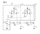
- FIG. 5 shows an exemplary embodiment of a circuit according to the invention, in which a current sensor 41 and a current source 51 are jointly realized as current mirrors.
- the current sensor 41 in this case forms an input transistor of the current mirror, while the current source 51 forms an output transistor of this current mirror.
- a current I41 flowing through the input transistor 41 is mapped in this arrangement via the output transistor 51 onto a current I51 at the control terminal 11 of the semiconductor switch T1.
- the current mirror 41, 51 can be of such a dimension that the current I41 corresponds to the current I51.
- the two current mirror transistors in the depicted example are configured as p-channel MOSFETs, of which the input transistor 41 is wired as a diode.
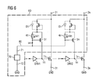
- the current sensor 41 of an actuating circuit is realized as an ohmic resistor, which are connected between the first load terminal 21 of the respective semiconductor switch T1 and the central circuit node 80.
- a current I41 flowing across this resistor 41 in event of an overload causes a voltage drop V41 across this resistor, which serves to actuate a transistor 51, whose load is connected between the first load terminal 21 and the control terminal 11 of the respective semiconductor switch T1.
- the transistor 51, 5n in this circuit according to Figure 6 functions as a current source and is configured in the example as a p-channel MOSFET.
- resistors 91, 9n may be connected between the rectifier elements D1, Dn and the gate terminals of the current mirror output transistors 51, 5n. These resistors serve to increase the robustness of the current sensors.
- the diodes D1, Dn are realized using the parasitic bulk - drain junction of a PMOS transistors. This permits an area saving since the diodes/rectifiers D1, Dn and the current sources 51, 5n can be placed into the same bulk.
- overvoltage protection arrangement of the circuit according to the invention merely requires, for protection of the semiconductor switches, a voltage limiting unit realized by using one or more Zener diodes.
- This overvoltage protection arrangement has the benefit of being space-saving, given the need to provide only one voltage limiting unit. Furthermore, no problems caused by manufacturing variations can arise in this overvoltage protection arrangement.
Landscapes
- Electronic Switches (AREA)
Abstract
- a voltage limiting unit (70) with a first and a second terminal (71, 72), whose first terminal is connected to a central circuit node (80), whose second terminal is connected to a terminal for a reference potential (GND), and which is configured so that, when a threshold voltage is applied between the first and second load terminals (71, 72), it conducts a current, and the central circuit node (80) is coupled to the first load terminals (21, 2n) of the semiconductor switches (T1, Tn),
- a first actuating circuit for the first semiconductor switch (T1) and a second actuating circuit for the at least one second semiconductor switch, each of the actuating circuits comprising a current sensor, which is connected between the first load terminal (21, 2n) of the particular semiconductor switch (T1, Tn) and the central circuit node, and a current source (51, 5n) which is actuated by the current sensor (41, 4n), being connected to the control terminal (11, 1n) of the particular semiconductor switch (T1, Tn).
Description
- The present invention relates to a circuit arrangement with at least two semiconductor switches and with an overvoltage protection for the at least two semiconductor switches.
- Semiconductor switches such as MOSFETs or IGBTs are being used increasingly for switching electrical loads, such as switching electrical consumers in motor vehicles. In order to be able to actuate several consumers by means of a single integrated circuit, several semiconductor switches, in particular several power MOSFETs, are integrated in a semiconductor chip. An integrated circuit with two power MOSFETs integrated in a chip is, for example, the integrated circuit HITFET® BTS 3410 G, which is described in data sheet 2004-03-05 of Infineon Technologies AG, Munich.
- Such an integrated circuit with several semiconductor switches has circuits available separately for each of the semiconductor switches. Such circuits are, for example, driver circuits, one of which is assigned to each semiconductor switch, or protection circuits, such as current limiting circuits, overheating circuits, overvoltage protection circuits, or circuits to prevent overloading, one of each being assigned to each semiconductor switch.
- The overvoltage protection circuits are, in particular, protection circuits working on the principle of "active Zenering". This principle is likewise presented in the above-mentioned data sheet for the BTS 3410 G and will be explained hereinbelow with reference to Figure 1.
- Figure 1 shows a circuit arrangement with two semiconductor switches T1, Tn, configured as a MOSFET, each of them having one
control terminal first load terminals second load terminals - To protect the semiconductor switches T1, Tn against an overvoltage between their
load terminals first load terminals control terminals first load terminal control terminals - The drawback in the solution explained by Figure 1 is that a separate overvoltage protection circuit has to be provided for each semiconductor switch, which requires a not insignificant surface area on the semiconductor chip to produce the protection circuits. This problem becomes worse with increasing number of semiconductor switches being integrated together in a single chip.
- Another problem with providing separate overvoltage protection circuits for the at least two semiconductor switches can arise in the situation represented by the dotted line in Figure 1, when the two semiconductor switches T1, Tn jointly actuate an inductive load L. The load in this case is connected between a terminal for a positive power supply potential V+ and the
first load terminals second load terminals - If, in this circuit configuration, the two semiconductor switches T1, Tn are caused to go into conduction, a load current will flow through the inductive load, being shared between the two semiconductor switches T1, Tn. If the two semiconductor switches T1, Tn are then switched off, the voltage on their
first load terminals control terminals first load terminals - If the Zener diodes Z1, Zn differ in their breakthrough voltage due to manufacturing variations, an operating situation may result in which one of the two semiconductor switches T1, Tn is conducting, while the other is still blocking. The conducting semiconductor switch will then have the entire commutation current of the inductive load flowing through it, which can result in an overstress that can lead to destruction of this semiconductor switch. In this connection, it should be noted that, instead of only one Zener diode, it is customary to provide series circuits of several Zener diodes, which somewhat aggravates the problem of manufacturing-caused variations.
- The object of the present invention is to provide a circuit arrangement with at least two semiconductor switches and an overvoltage protection arrangement in which the overvoltage protection arrangement is economical in space and in which the at least two semiconductor switches are reliably protected against overvoltages.
- This object is met by a circuit arrangement according to
Claim 1. Advantageous embodiments of the invention are the subjects of the dependent claims. - The circuit arrangement according to the invention comprises a first semiconductor switch and at least one second semiconductor switch, each of them having a control terminal and a first and a second load terminal, and an overvoltage protection arrangement for the at least two semiconductor switches. The overvoltage protection arrangement has a voltage limiting unit with a first and a second terminal, whose first terminal is connected to a central circuit node and whose second terminal is connected to a terminal for a reference potential. The voltage limiting unit is configured so that, when a predetermined threshold voltage is applied between the first and second load terminals, it conducts a current. The overvoltage protection arrangement, furthermore, has a first actuating circuit for the first semiconductor switch and a second actuating circuit for the at least one second semiconductor switch. Each of these actuating circuits comprises a current sensor, which is connected between the first load terminal of the particular semiconductor switch and the central circuit node, and a current source which is actuated by the current sensor, being connected to the control terminal of the particular semiconductor switch.
- In this overvoltage protection arrangement, where the voltage limiting unit is coupled via the central circuit node to the first load terminals of the semiconductor switches, the voltage limiting unit conducts a current when the potential at the first load terminal rises by the value of the threshold voltage of the voltage limiting unit above the value of a reference potential. This current flowing across the voltage limiting unit serves the purpose, via the current sensor and the current source of the actuating circuit belonging to this semiconductor switch, of biasing this semiconductor switch into conduction in order to counteract a further rising of the potential of the load portion of the circuit.
- The voltage limiting unit in this circuit arrangement can comprise a Zener diode or a series connection with several Zener diodes. The breakthrough voltage of this Zener diode or of the series connection with several Zener diodes will determine the threshold voltage at which a current will flow from the central circuit node, to which all of the first load terminals of the semiconductor switches are connected to, across the voltage limiting unit.
- As an alternative, it is possible to provide an additional semiconductor switch in the voltage limiting unit, which is actuated by a Zener diode or by a series connection with several Zener diodes.
- In one embodiment, the current sensor and the current source of the actuating circuit of a semiconductor switch are realized such that they form a current mirror, which maps a current flowing from the first load terminal of the particular semiconductor switch to the central circuit node onto a current at the control terminal of the particular semiconductor switch.
- In another embodiment, the current sensor of the actuating circuit of a semiconductor switch is realized as a resistor and the current source as a transistor, which is controlled by a voltage drop across the resistor.
- The present invention will now be explained in greater detail with reference to the drawings.
- Figure 1
- shows a circuit arrangement with two semiconductor switches according to the prior art, each of which is connected to its own overvoltage protection circuit.
- Figure 2
- shows the electrical equivalent diagram of a circuit arrangement according to the invention with at least two semiconductor switches, having a central overvoltage protection arrangement for the semiconductor switches.
- Figure 3
- shows a first exemplary embodiment of a voltage limiting unit of the overvoltage protection arrangement.
- Figure 4
- shows a second exemplary embodiment of a voltage limiting unit of the overvoltage protection arrangement.
- Figure 5
- shows a second exemplary embodiment of a circuit arrangement according to the invention.
- Figure 6
- shows a third exemplary embodiment of a circuit arrangement according to the invention.
- In the figures, unless otherwise stated, the same reference numbers designate the same circuit components and signals with the same meaning.
- Figure 2 shows a first exemplary embodiment of a circuit arrangement according to the invention, having two semiconductor switches T1, Tn, each of which has a
control terminal first load terminal second load terminal first load terminals second load terminals control terminals - To each of the
control terminals - The two semiconductor switches T1, Tn can be actuated separately from each other via the actuating signals IN1, INn and thereby serve to actuate different loads, not shown in greater detail in Figure 2, independently of each other. These loads are to be connected in series with the load paths of the semiconductor switches T1, Tn with these series circuits are to be connected between terminals for a power supply potential and a reference potential.
- The two semiconductor switches T1, Tn and their driver circuits DRV1, DRVn are integrated in a manner not depicted in greater detail, preferably jointly in a semiconductor body or a semiconductor chip.
- A common
overvoltage protection circuit 60 is provided to protect the two semiconductor switches T1, Tn against overvoltage on their load sections. Thisovervoltage protection circuit 60 comprises avoltage limiting unit 70 with a first and asecond terminal first terminal 71 being connected to acentral circuit node 80 and thesecond terminal 72 being connected to a terminal for a reference potential GND. This reference potential GND can be, in particular, the reference potential to which all voltages are referred in an application circuit in which the depicted circuit arrangement is employed. This reference potential GND can be, in particular, the ground potential. - The
first terminal 71 of the voltage limiting unit is coupled via thecentral circuit node 80 to thefirst load terminals first load terminals central circuit node 80 there is connected acurrent sensor current sensors current source control terminal current sources first load terminals control terminals first load terminals - In a manner not shown in greater detail, it is also possible to connect the
terminals control terminals - In the context of the present invention, "current source" signifies a circuit arrangement that is controlled by one of the current sensors and furnishes a current to the control terminal of the respective semiconductor switch. This current source can also be realized, in a manner not specifically illustrated, as a switch that is controlled by the respective current sensor and whose load path is connected between a terminal for a power supply potential and the control terminal of the respective semiconductor switch.
- Optionally, rectifiers D1, Dn are connected between the
first load terminals current sensors central circuit node 80 across the load paths of the semiconductor switches T1, Tn. - The functioning of the circuit arrangement depicted in Figure 2 will now be explained by means of the first semiconductor switch T1 and its actuation circuit, which comprises the
current sensor 41 and thecurrent source 51. For this, let it first be assumed that the semiconductor switch T1 is actuated into blocking via the actuation signal IN1 and the driver circuit DRV1. If, during this process, the load potential at the first load terminal 21 - for example, due to an inductive load connected to it - increases to a value that corresponds to the threshold voltage of thevoltage limiting unit 70 plus the forward voltage of the diode D1, a current I41 will flow from thefirst load terminal 21 across the diode D1, thecurrent sensor 41, and thevoltage limiting unit 70 to reference potential GND. Thecurrent sensor 41 detects this current flow and actuates thecurrent source 51, so that the latter delivers a current I51 to thecontrol terminal 11 of the semiconductor switch T1. The semiconductor switch T1 is thereby biased into conduction so as to counteract any further rise in the load potential or, in case of an inductive load connected to thefirst load terminal 21, to commutate this inductive load away. - The overvoltage protection function explained above operates accordingly for the second semiconductor switch Tn, when a potential rises at the
first load terminal 2n of this second semiconductor switch Tn. In this case, thecurrent sensor 4n actuates thecurrent source 5n hooked up to thecontrol terminal 1n of this semiconductor switch Tn, thereby biasing the semiconductor switch Tn into conduction. The overvoltage protection function in this overvoltage protection circuit is also present when the load potentials at both semiconductor switches T1, Tn increase to values above the threshold voltage of thevoltage limiting unit 70. In this case, currents flow from bothfirst load terminals current sensors voltage limiting unit 70 to reference potential GND. These currents are detected by thecurrent sensors current sources - The circuit arrangement depicted in Figure 2 contains two "channels", each with a semiconductor switch. This circuit, of course, can be expanded to more than two semiconductor switches T1, Tn, as suggested in Figure 2. Each "channel" added in addition to this circuit comprises a semiconductor switch with a driver circuit, as well as an actuating circuit, having a current sensor and a current source. The current sensor is connected, similarly to the
current sensors central circuit node 80. - Figure 3 shows one possible exemplary embodiment for the
voltage limiting unit 70. The voltage limiting unit in this case has a series circuit withseveral Zener diodes second terminals several Zener diodes voltage limiting unit 70 will conduct a current between the first andsecond terminal - Figure 4 shows another exemplary embodiment of such a voltage limiting unit. The voltage limiting unit in this case has a series circuit of
several Zener diodes resistor 84 between the first andsecond terminals channel MOSFET 85. ThisMOSFET 85 is actuated by a voltage V84 across theresistor 84 and is conducting when the voltage between the first andsecond terminals MOSFET 85. Since the threshold resistance of theMOSFET 85 is lower than the forward resistance of the Zener diode chain operating in the blocking direction, theMOSFET 85 takes up the main share of the current flowing between the first andsecond terminals additional MOSFET 85, the voltage limiting unit of Figure 4 is more space-saving. Furthermore, the clamping voltage of the voltage limiting unit 73 in Figure 4 is less dependant on the currents I41, ..., I4n flowing into the voltage limiting unit 73. - Figure 5 shows an exemplary embodiment of a circuit according to the invention, in which a
current sensor 41 and acurrent source 51 are jointly realized as current mirrors. Thecurrent sensor 41 in this case forms an input transistor of the current mirror, while thecurrent source 51 forms an output transistor of this current mirror. A current I41 flowing through theinput transistor 41 is mapped in this arrangement via theoutput transistor 51 onto a current I51 at thecontrol terminal 11 of the semiconductor switch T1. Thecurrent mirror transistors input transistor 41 is wired as a diode. - Another exemplary embodiment of the current sensors and the current sources is given in Figure 6. In this exemplary embodiment, the
current sensor 41 of an actuating circuit is realized as an ohmic resistor, which are connected between thefirst load terminal 21 of the respective semiconductor switch T1 and thecentral circuit node 80. A current I41 flowing across thisresistor 41 in event of an overload causes a voltage drop V41 across this resistor, which serves to actuate atransistor 51, whose load is connected between thefirst load terminal 21 and thecontrol terminal 11 of the respective semiconductor switch T1. Thetransistor - Also a mixed solution comprising a current mirror and a resistor may be used as a current sensor. Referring to Figure 5
resistors mirror output transistors - In the exemplary embodiment of Figure 6 the diodes D1, Dn are realized using the parasitic bulk - drain junction of a PMOS transistors. This permits an area saving since the diodes/rectifiers D1, Dn and the
current sources - The above-described overvoltage protection arrangement of the circuit according to the invention merely requires, for protection of the semiconductor switches, a voltage limiting unit realized by using one or more Zener diodes. This overvoltage protection arrangement has the benefit of being space-saving, given the need to provide only one voltage limiting unit. Furthermore, no problems caused by manufacturing variations can arise in this overvoltage protection arrangement.
-
- V+
- positive power supply potential
- GND
- reference potential
- IN1, INn
- input signals
- DRV1, DRVn
- driver circuits
- L
- inductive load
- 11, 1n
- control terminals, gate terminals
- Z1, Zn
- Zener diodes
- D1, Dn
- diodes
- 21, 2n
- first load terminals
- 31, 3n
- second load terminals
- T1, Tn
- semiconductor switches, n-channel-MOSFET
- 60
- overvoltage protection arrangement
- 80
- central circuit node
- 70
- voltage limiting unit
- 71, 72
- terminals of the voltage limiting unit
- 81-83
- Zener diodes
- 84
- resistor
- V84
- voltage
- 85
- semiconductor switch, n-channel-MOSFET
- 91, 9n
- resistors
- I41, I4n
- currents
- V41, V4n
- voltages
Claims (8)
- Circuit arrangement witha first semiconductor switch (T1) and at least one second semiconductor switch (Tn), each of them having a control terminal (11, 1n) and a first (21, 2n) and second (31, 3n) load terminal, and withan overvoltage protection arrangement (60) for the at least two semiconductor switches (T1, Tn), having:- a voltage limiting unit (70) with a first and a second terminal (71, 72), whose first terminal is connected to a central circuit node (80), whose second terminal is connected to a terminal for a reference potential (GND), and which is configured so that, when a threshold voltage is applied between the first and second load terminals (71, 72), it conducts a current, and the central circuit node (80) is coupled to the first load terminals (21, 2n) of the semiconductor switches (T1, Tn),- a first actuating circuit for the first semiconductor switch (T1) and a second actuating circuit for the at least one second semiconductor switch, each of the actuating circuits comprising a current sensor, which is connected between the first load terminal (21, 2n) of the particular semiconductor switch (T1, Tn) and the central circuit node, and a current source (51, 5n) which is actuated by the current sensor (41, 4n), being connected to the control terminal (11, 1n) of the particular semiconductor switch (T1, Tn).
- Circuit arrangement according to Claim 1, in which the current limiting unit (70) has at least one Zener diode (81, 82, 83), having a load section, which are connected between the terminals (71, 72) of the voltage limiting unit (70).
- Circuit arrangement according to Claim 2, in which the voltage limiting unit comprises several Zener diodes (81, 82, 83), each with a load section, whose load sections are connected in series between the terminals (71, 72) of the voltage limiting unit (70).
- Circuit arrangement according to Claim 1, in which the voltage limiting unit (70) comprises:- a semiconductor switch (85) with a control terminal and a load section, whose load section is connected between the terminals (71, 72) of the voltage limiting unit (70),- an activation circuit (73) for the semiconductor switch (85), which is connected between the terminals (71, 72) of the voltage limiting unit and which is designed to make the semiconductor switch become conducting depending on a voltage between these terminals (71, 72).
- Circuit arrangement according to Claim 4, in which the activation circuit (73) of the voltage limiting unit (70) has a series circuit with at least one Zener diode (81, 82, 83) and with a resistor (84), which is connected between the terminals (71, 72) of the voltage limiting unit (70), and the control terminal of the semiconductor switch (85) is connected to a node common to the at least one Zener diode (81, 82, 83) and the resistor (84).
- Circuit arrangement according to one of the foregoing claims, in which a rectifier (D1, Dn) is connected each time between the first load terminal of the first and second semiconductor switches (T1, Tn) and the central circuit node (80).
- Circuit arrangement according to one of the foregoing claims, in which the current sensor (41, 4n) and the current source (51, 5n) of an actuating circuit form a current mirror, which maps a current flowing from the first load terminal (21, 2n) of the particular semiconductor switch (T1, Tn) to the central circuit node (80) onto a current at the control terminal of the particular semiconductor switch (T1, Tn).
- Circuit arrangement according to one of Claims 1 to 6, in which the current sensor (41, 4n) of an actuating circuit is realized as a resistor and the current source (51, 5n) is realized as a transistor, which is controlled by a voltage drop across the resistor (41, 4n).
Priority Applications (3)
| Application Number | Priority Date | Filing Date | Title |
|---|---|---|---|
| DE602005006584T DE602005006584D1 (en) | 2005-11-04 | 2005-11-04 | Arrangement with at least two semiconductor switches and a common overvoltage protection |
| EP05024090A EP1783909B1 (en) | 2005-11-04 | 2005-11-04 | Circuit arrangement with at least two semiconductor switches and a central overvoltage protection |
| US11/364,835 US7411770B2 (en) | 2005-11-04 | 2006-02-28 | Circuit arrangement with at least two semiconductor switches and a central overvoltage protection |
Applications Claiming Priority (1)
| Application Number | Priority Date | Filing Date | Title |
|---|---|---|---|
| EP05024090A EP1783909B1 (en) | 2005-11-04 | 2005-11-04 | Circuit arrangement with at least two semiconductor switches and a central overvoltage protection |
Publications (2)
| Publication Number | Publication Date |
|---|---|
| EP1783909A1 true EP1783909A1 (en) | 2007-05-09 |
| EP1783909B1 EP1783909B1 (en) | 2008-05-07 |
Family
ID=35406202
Family Applications (1)
| Application Number | Title | Priority Date | Filing Date |
|---|---|---|---|
| EP05024090A Ceased EP1783909B1 (en) | 2005-11-04 | 2005-11-04 | Circuit arrangement with at least two semiconductor switches and a central overvoltage protection |
Country Status (3)
| Country | Link |
|---|---|
| US (1) | US7411770B2 (en) |
| EP (1) | EP1783909B1 (en) |
| DE (1) | DE602005006584D1 (en) |
Cited By (4)
| Publication number | Priority date | Publication date | Assignee | Title |
|---|---|---|---|---|
| DE102007053405A1 (en) * | 2007-11-09 | 2009-05-28 | Continental Automotive Gmbh | Integrated circuit arrangement i.e. power output stage, for use in automobile, has controllable connection device for selectively connecting control connections of switching transistors, which belongs to different switching devices |
| DE102008060793A1 (en) | 2008-12-05 | 2010-06-10 | Continental Automotive Gmbh | Circuit arrangement for use as multi-power output stage for switching excitation winding of solenoid valve, in automobile electronics field, has controllable connection device connecting nodes of respective transistors with one another |
| CN109217278A (en) * | 2018-11-20 | 2019-01-15 | 上海艾为电子技术股份有限公司 | Surge protection circuit, system and equipment |
| DE102015225378B4 (en) | 2014-12-17 | 2019-03-28 | Denso Corporation | FUEL INJECTION CONTROL |
Families Citing this family (4)
| Publication number | Priority date | Publication date | Assignee | Title |
|---|---|---|---|---|
| EP1873917A1 (en) * | 2006-06-30 | 2008-01-02 | Infineon Technologies Austria AG | Circuit arrangment with at least two semiconductor switches |
| JP5363879B2 (en) * | 2009-06-03 | 2013-12-11 | ルネサスエレクトロニクス株式会社 | Driver circuit |
| DE102010030064B4 (en) | 2010-06-15 | 2022-04-28 | Infineon Technologies Ag | protection circuit |
| JP6171599B2 (en) * | 2013-06-11 | 2017-08-02 | サンケン電気株式会社 | Semiconductor device and control method thereof |
Citations (2)
| Publication number | Priority date | Publication date | Assignee | Title |
|---|---|---|---|---|
| DE4225408C1 (en) * | 1992-07-31 | 1994-04-28 | Siemens Nixdorf Inf Syst | Overvoltage protection for push=pull transistor switching stage - uses respective diodes for each transistor and common Zener diode coupled between transistor drain and control electrodes |
| US20050088216A1 (en) * | 2003-08-28 | 2005-04-28 | Infineon Technologies Ag | Circuit arrangement having a load transistor and a voltage limiting circuit and method for driving a load transistor |
-
2005
- 2005-11-04 DE DE602005006584T patent/DE602005006584D1/en not_active Expired - Lifetime
- 2005-11-04 EP EP05024090A patent/EP1783909B1/en not_active Ceased
-
2006
- 2006-02-28 US US11/364,835 patent/US7411770B2/en active Active
Patent Citations (2)
| Publication number | Priority date | Publication date | Assignee | Title |
|---|---|---|---|---|
| DE4225408C1 (en) * | 1992-07-31 | 1994-04-28 | Siemens Nixdorf Inf Syst | Overvoltage protection for push=pull transistor switching stage - uses respective diodes for each transistor and common Zener diode coupled between transistor drain and control electrodes |
| US20050088216A1 (en) * | 2003-08-28 | 2005-04-28 | Infineon Technologies Ag | Circuit arrangement having a load transistor and a voltage limiting circuit and method for driving a load transistor |
Cited By (6)
| Publication number | Priority date | Publication date | Assignee | Title |
|---|---|---|---|---|
| DE102007053405A1 (en) * | 2007-11-09 | 2009-05-28 | Continental Automotive Gmbh | Integrated circuit arrangement i.e. power output stage, for use in automobile, has controllable connection device for selectively connecting control connections of switching transistors, which belongs to different switching devices |
| DE102008060793A1 (en) | 2008-12-05 | 2010-06-10 | Continental Automotive Gmbh | Circuit arrangement for use as multi-power output stage for switching excitation winding of solenoid valve, in automobile electronics field, has controllable connection device connecting nodes of respective transistors with one another |
| DE102008060793B4 (en) * | 2008-12-05 | 2010-09-02 | Continental Automotive Gmbh | Circuit arrangement for switching one or more inductive loads |
| DE102015225378B4 (en) | 2014-12-17 | 2019-03-28 | Denso Corporation | FUEL INJECTION CONTROL |
| CN109217278A (en) * | 2018-11-20 | 2019-01-15 | 上海艾为电子技术股份有限公司 | Surge protection circuit, system and equipment |
| CN109217278B (en) * | 2018-11-20 | 2023-09-22 | 上海艾为电子技术股份有限公司 | Surge protection circuit, circuit system and electronic equipment |
Also Published As
| Publication number | Publication date |
|---|---|
| EP1783909B1 (en) | 2008-05-07 |
| US7411770B2 (en) | 2008-08-12 |
| DE602005006584D1 (en) | 2008-06-19 |
| US20070103830A1 (en) | 2007-05-10 |
Similar Documents
| Publication | Publication Date | Title |
|---|---|---|
| EP2071724B1 (en) | Power supply control circuit | |
| JP5383426B2 (en) | Rapid discharge circuit when abnormality is detected | |
| JP5274823B2 (en) | Power supply control circuit | |
| US7535283B2 (en) | Gate drive circuit, semiconductor module and method for driving switching element | |
| US7453308B2 (en) | Circuit arrangement having a load transistor and a voltage limiting circuit and method for driving a load transistor | |
| US20080002324A1 (en) | Circuit arrangement with at least two semiconductor switches | |
| US8953294B2 (en) | Circuit arrangement with an overcurrent fuse | |
| US20060113838A1 (en) | Power semiconductor device | |
| US20150145583A1 (en) | Semiconductor device | |
| US20090154035A1 (en) | ESD Protection Circuit | |
| JP2014138521A (en) | Driving device for semiconductor element | |
| EP1783909B1 (en) | Circuit arrangement with at least two semiconductor switches and a central overvoltage protection | |
| EP3035531B1 (en) | Semiconductor device and current limiting method | |
| JP2009207077A (en) | Semiconductor integrated circuit device | |
| JP4271169B2 (en) | Semiconductor device | |
| JP5360304B2 (en) | Semiconductor device | |
| US7492561B2 (en) | Protective circuit | |
| US6246557B1 (en) | Loss of ground protection for electronic relays | |
| JP3983622B2 (en) | Power device drive circuit | |
| JP4479570B2 (en) | Switching circuit with protection function and protection circuit | |
| US12580558B2 (en) | Device, half bridge and method for operating a device | |
| CN112671053A (en) | Electronic circuit with dual voltage supply circuit | |
| JP3676168B2 (en) | Power supply control device | |
| US20230073508A1 (en) | Semiconductor device | |
| JP2008061339A (en) | Inverter circuit |
Legal Events
| Date | Code | Title | Description |
|---|---|---|---|
| PUAI | Public reference made under article 153(3) epc to a published international application that has entered the european phase |
Free format text: ORIGINAL CODE: 0009012 |
|
| 17P | Request for examination filed |
Effective date: 20060131 |
|
| AK | Designated contracting states |
Kind code of ref document: A1 Designated state(s): AT BE BG CH CY CZ DE DK EE ES FI FR GB GR HU IE IS IT LI LT LU LV MC NL PL PT RO SE SI SK TR |
|
| AX | Request for extension of the european patent |
Extension state: AL BA HR MK YU |
|
| GRAP | Despatch of communication of intention to grant a patent |
Free format text: ORIGINAL CODE: EPIDOSNIGR1 |
|
| GRAS | Grant fee paid |
Free format text: ORIGINAL CODE: EPIDOSNIGR3 |
|
| AKX | Designation fees paid |
Designated state(s): DE FR GB IT |
|
| GRAA | (expected) grant |
Free format text: ORIGINAL CODE: 0009210 |
|
| AK | Designated contracting states |
Kind code of ref document: B1 Designated state(s): DE FR GB IT |
|
| REG | Reference to a national code |
Ref country code: GB Ref legal event code: FG4D |
|
| REF | Corresponds to: |
Ref document number: 602005006584 Country of ref document: DE Date of ref document: 20080619 Kind code of ref document: P |
|
| PLBE | No opposition filed within time limit |
Free format text: ORIGINAL CODE: 0009261 |
|
| STAA | Information on the status of an ep patent application or granted ep patent |
Free format text: STATUS: NO OPPOSITION FILED WITHIN TIME LIMIT |
|
| 26N | No opposition filed |
Effective date: 20090210 |
|
| REG | Reference to a national code |
Ref country code: FR Ref legal event code: PLFP Year of fee payment: 11 |
|
| REG | Reference to a national code |
Ref country code: FR Ref legal event code: PLFP Year of fee payment: 12 |
|
| REG | Reference to a national code |
Ref country code: FR Ref legal event code: PLFP Year of fee payment: 13 |
|
| PGFP | Annual fee paid to national office [announced via postgrant information from national office to epo] |
Ref country code: FR Payment date: 20191120 Year of fee payment: 15 Ref country code: IT Payment date: 20191128 Year of fee payment: 15 |
|
| PG25 | Lapsed in a contracting state [announced via postgrant information from national office to epo] |
Ref country code: IT Free format text: LAPSE BECAUSE OF NON-PAYMENT OF DUE FEES Effective date: 20201104 Ref country code: FR Free format text: LAPSE BECAUSE OF NON-PAYMENT OF DUE FEES Effective date: 20201130 |
|
| P01 | Opt-out of the competence of the unified patent court (upc) registered |
Effective date: 20230528 |
|
| PGFP | Annual fee paid to national office [announced via postgrant information from national office to epo] |
Ref country code: GB Payment date: 20231123 Year of fee payment: 19 |
|
| PGFP | Annual fee paid to national office [announced via postgrant information from national office to epo] |
Ref country code: DE Payment date: 20240122 Year of fee payment: 19 |
|
| REG | Reference to a national code |
Ref country code: DE Ref legal event code: R119 Ref document number: 602005006584 Country of ref document: DE |
|
| GBPC | Gb: european patent ceased through non-payment of renewal fee |
Effective date: 20241104 |
|
| PG25 | Lapsed in a contracting state [announced via postgrant information from national office to epo] |
Ref country code: DE Free format text: LAPSE BECAUSE OF NON-PAYMENT OF DUE FEES Effective date: 20250603 |
|
| PG25 | Lapsed in a contracting state [announced via postgrant information from national office to epo] |
Ref country code: GB Free format text: LAPSE BECAUSE OF NON-PAYMENT OF DUE FEES Effective date: 20241104 |