EP1782526B1 - Device for feeding auxiliary operating devices for a fuel electric vehicle - Google Patents
Device for feeding auxiliary operating devices for a fuel electric vehicle Download PDFInfo
- Publication number
- EP1782526B1 EP1782526B1 EP05771357A EP05771357A EP1782526B1 EP 1782526 B1 EP1782526 B1 EP 1782526B1 EP 05771357 A EP05771357 A EP 05771357A EP 05771357 A EP05771357 A EP 05771357A EP 1782526 B1 EP1782526 B1 EP 1782526B1
- Authority
- EP
- European Patent Office
- Prior art keywords
- voltage
- rectifier
- connection
- circuit
- direct voltage
- Prior art date
- Legal status (The legal status is an assumption and is not a legal conclusion. Google has not performed a legal analysis and makes no representation as to the accuracy of the status listed.)
- Active
Links
- 239000000446 fuel Substances 0.000 title claims 3
- 239000004065 semiconductor Substances 0.000 claims description 49
- 238000002485 combustion reaction Methods 0.000 claims description 15
- 239000003990 capacitor Substances 0.000 claims 2
- 230000000670 limiting effect Effects 0.000 description 27
- 230000010355 oscillation Effects 0.000 description 12
- 238000012423 maintenance Methods 0.000 description 8
- 230000006378 damage Effects 0.000 description 4
- 238000002955 isolation Methods 0.000 description 4
- 230000000694 effects Effects 0.000 description 3
- 238000009434 installation Methods 0.000 description 3
- 238000000926 separation method Methods 0.000 description 3
- 238000010276 construction Methods 0.000 description 2
- 238000013461 design Methods 0.000 description 2
- 238000009413 insulation Methods 0.000 description 2
- 238000011017 operating method Methods 0.000 description 2
- 238000004378 air conditioning Methods 0.000 description 1
- 230000000903 blocking effect Effects 0.000 description 1
- 230000001419 dependent effect Effects 0.000 description 1
- 238000011161 development Methods 0.000 description 1
- 230000018109 developmental process Effects 0.000 description 1
- 230000001939 inductive effect Effects 0.000 description 1
- 230000003137 locomotive effect Effects 0.000 description 1
- 238000005065 mining Methods 0.000 description 1
- 230000001681 protective effect Effects 0.000 description 1
Images


Classifications
-
- H—ELECTRICITY
- H02—GENERATION; CONVERSION OR DISTRIBUTION OF ELECTRIC POWER
- H02M—APPARATUS FOR CONVERSION BETWEEN AC AND AC, BETWEEN AC AND DC, OR BETWEEN DC AND DC, AND FOR USE WITH MAINS OR SIMILAR POWER SUPPLY SYSTEMS; CONVERSION OF DC OR AC INPUT POWER INTO SURGE OUTPUT POWER; CONTROL OR REGULATION THEREOF
- H02M3/00—Conversion of dc power input into dc power output
- H02M3/02—Conversion of dc power input into dc power output without intermediate conversion into ac
- H02M3/04—Conversion of dc power input into dc power output without intermediate conversion into ac by static converters
- H02M3/10—Conversion of dc power input into dc power output without intermediate conversion into ac by static converters using discharge tubes with control electrode or semiconductor devices with control electrode
- H02M3/145—Conversion of dc power input into dc power output without intermediate conversion into ac by static converters using discharge tubes with control electrode or semiconductor devices with control electrode using devices of a triode or transistor type requiring continuous application of a control signal
- H02M3/155—Conversion of dc power input into dc power output without intermediate conversion into ac by static converters using discharge tubes with control electrode or semiconductor devices with control electrode using devices of a triode or transistor type requiring continuous application of a control signal using semiconductor devices only
- H02M3/156—Conversion of dc power input into dc power output without intermediate conversion into ac by static converters using discharge tubes with control electrode or semiconductor devices with control electrode using devices of a triode or transistor type requiring continuous application of a control signal using semiconductor devices only with automatic control of output voltage or current, e.g. switching regulators
- H02M3/158—Conversion of dc power input into dc power output without intermediate conversion into ac by static converters using discharge tubes with control electrode or semiconductor devices with control electrode using devices of a triode or transistor type requiring continuous application of a control signal using semiconductor devices only with automatic control of output voltage or current, e.g. switching regulators including plural semiconductor devices as final control devices for a single load
- H02M3/1584—Conversion of dc power input into dc power output without intermediate conversion into ac by static converters using discharge tubes with control electrode or semiconductor devices with control electrode using devices of a triode or transistor type requiring continuous application of a control signal using semiconductor devices only with automatic control of output voltage or current, e.g. switching regulators including plural semiconductor devices as final control devices for a single load with a plurality of power processing stages connected in parallel
-
- B—PERFORMING OPERATIONS; TRANSPORTING
- B60—VEHICLES IN GENERAL
- B60L—PROPULSION OF ELECTRICALLY-PROPELLED VEHICLES; SUPPLYING ELECTRIC POWER FOR AUXILIARY EQUIPMENT OF ELECTRICALLY-PROPELLED VEHICLES; ELECTRODYNAMIC BRAKE SYSTEMS FOR VEHICLES IN GENERAL; MAGNETIC SUSPENSION OR LEVITATION FOR VEHICLES; MONITORING OPERATING VARIABLES OF ELECTRICALLY-PROPELLED VEHICLES; ELECTRIC SAFETY DEVICES FOR ELECTRICALLY-PROPELLED VEHICLES
- B60L50/00—Electric propulsion with power supplied within the vehicle
- B60L50/10—Electric propulsion with power supplied within the vehicle using propulsion power supplied by engine-driven generators, e.g. generators driven by combustion engines
- B60L50/15—Electric propulsion with power supplied within the vehicle using propulsion power supplied by engine-driven generators, e.g. generators driven by combustion engines with additional electric power supply
-
- H—ELECTRICITY
- H02—GENERATION; CONVERSION OR DISTRIBUTION OF ELECTRIC POWER
- H02M—APPARATUS FOR CONVERSION BETWEEN AC AND AC, BETWEEN AC AND DC, OR BETWEEN DC AND DC, AND FOR USE WITH MAINS OR SIMILAR POWER SUPPLY SYSTEMS; CONVERSION OF DC OR AC INPUT POWER INTO SURGE OUTPUT POWER; CONTROL OR REGULATION THEREOF
- H02M3/00—Conversion of dc power input into dc power output
- H02M3/02—Conversion of dc power input into dc power output without intermediate conversion into ac
- H02M3/04—Conversion of dc power input into dc power output without intermediate conversion into ac by static converters
- H02M3/10—Conversion of dc power input into dc power output without intermediate conversion into ac by static converters using discharge tubes with control electrode or semiconductor devices with control electrode
- H02M3/145—Conversion of dc power input into dc power output without intermediate conversion into ac by static converters using discharge tubes with control electrode or semiconductor devices with control electrode using devices of a triode or transistor type requiring continuous application of a control signal
- H02M3/155—Conversion of dc power input into dc power output without intermediate conversion into ac by static converters using discharge tubes with control electrode or semiconductor devices with control electrode using devices of a triode or transistor type requiring continuous application of a control signal using semiconductor devices only
- H02M3/156—Conversion of dc power input into dc power output without intermediate conversion into ac by static converters using discharge tubes with control electrode or semiconductor devices with control electrode using devices of a triode or transistor type requiring continuous application of a control signal using semiconductor devices only with automatic control of output voltage or current, e.g. switching regulators
- H02M3/158—Conversion of dc power input into dc power output without intermediate conversion into ac by static converters using discharge tubes with control electrode or semiconductor devices with control electrode using devices of a triode or transistor type requiring continuous application of a control signal using semiconductor devices only with automatic control of output voltage or current, e.g. switching regulators including plural semiconductor devices as final control devices for a single load
-
- B—PERFORMING OPERATIONS; TRANSPORTING
- B60—VEHICLES IN GENERAL
- B60L—PROPULSION OF ELECTRICALLY-PROPELLED VEHICLES; SUPPLYING ELECTRIC POWER FOR AUXILIARY EQUIPMENT OF ELECTRICALLY-PROPELLED VEHICLES; ELECTRODYNAMIC BRAKE SYSTEMS FOR VEHICLES IN GENERAL; MAGNETIC SUSPENSION OR LEVITATION FOR VEHICLES; MONITORING OPERATING VARIABLES OF ELECTRICALLY-PROPELLED VEHICLES; ELECTRIC SAFETY DEVICES FOR ELECTRICALLY-PROPELLED VEHICLES
- B60L2200/00—Type of vehicles
- B60L2200/26—Rail vehicles
-
- B—PERFORMING OPERATIONS; TRANSPORTING
- B60—VEHICLES IN GENERAL
- B60L—PROPULSION OF ELECTRICALLY-PROPELLED VEHICLES; SUPPLYING ELECTRIC POWER FOR AUXILIARY EQUIPMENT OF ELECTRICALLY-PROPELLED VEHICLES; ELECTRODYNAMIC BRAKE SYSTEMS FOR VEHICLES IN GENERAL; MAGNETIC SUSPENSION OR LEVITATION FOR VEHICLES; MONITORING OPERATING VARIABLES OF ELECTRICALLY-PROPELLED VEHICLES; ELECTRIC SAFETY DEVICES FOR ELECTRICALLY-PROPELLED VEHICLES
- B60L2210/00—Converter types
- B60L2210/10—DC to DC converters
- B60L2210/12—Buck converters
-
- Y—GENERAL TAGGING OF NEW TECHNOLOGICAL DEVELOPMENTS; GENERAL TAGGING OF CROSS-SECTIONAL TECHNOLOGIES SPANNING OVER SEVERAL SECTIONS OF THE IPC; TECHNICAL SUBJECTS COVERED BY FORMER USPC CROSS-REFERENCE ART COLLECTIONS [XRACs] AND DIGESTS
- Y02—TECHNOLOGIES OR APPLICATIONS FOR MITIGATION OR ADAPTATION AGAINST CLIMATE CHANGE
- Y02T—CLIMATE CHANGE MITIGATION TECHNOLOGIES RELATED TO TRANSPORTATION
- Y02T10/00—Road transport of goods or passengers
- Y02T10/60—Other road transportation technologies with climate change mitigation effect
- Y02T10/70—Energy storage systems for electromobility, e.g. batteries
-
- Y—GENERAL TAGGING OF NEW TECHNOLOGICAL DEVELOPMENTS; GENERAL TAGGING OF CROSS-SECTIONAL TECHNOLOGIES SPANNING OVER SEVERAL SECTIONS OF THE IPC; TECHNICAL SUBJECTS COVERED BY FORMER USPC CROSS-REFERENCE ART COLLECTIONS [XRACs] AND DIGESTS
- Y02—TECHNOLOGIES OR APPLICATIONS FOR MITIGATION OR ADAPTATION AGAINST CLIMATE CHANGE
- Y02T—CLIMATE CHANGE MITIGATION TECHNOLOGIES RELATED TO TRANSPORTATION
- Y02T10/00—Road transport of goods or passengers
- Y02T10/60—Other road transportation technologies with climate change mitigation effect
- Y02T10/7072—Electromobility specific charging systems or methods for batteries, ultracapacitors, supercapacitors or double-layer capacitors
-
- Y—GENERAL TAGGING OF NEW TECHNOLOGICAL DEVELOPMENTS; GENERAL TAGGING OF CROSS-SECTIONAL TECHNOLOGIES SPANNING OVER SEVERAL SECTIONS OF THE IPC; TECHNICAL SUBJECTS COVERED BY FORMER USPC CROSS-REFERENCE ART COLLECTIONS [XRACs] AND DIGESTS
- Y02—TECHNOLOGIES OR APPLICATIONS FOR MITIGATION OR ADAPTATION AGAINST CLIMATE CHANGE
- Y02T—CLIMATE CHANGE MITIGATION TECHNOLOGIES RELATED TO TRANSPORTATION
- Y02T10/00—Road transport of goods or passengers
- Y02T10/60—Other road transportation technologies with climate change mitigation effect
- Y02T10/72—Electric energy management in electromobility
Definitions
- the invention relates to the field of auxiliary equipment for fuel-electrically driven vehicles. It is based on a device for feeding auxiliary equipment for a fuel-electrically driven vehicle according to the preamble of the independent claims.
- auxiliary equipment for fuel-electrically driven vehicles are used today mainly in diesel-electric locomotives or large diesel-electric mining vehicles, the auxiliary equipment, as a fan, air conditioners, servomotors, auxiliary power converters, etc., are formed. Such auxiliary equipment is commonly fed by a suitable device.
- a suitable device for feeding auxiliary equipment for a fuel-electric vehicle is for example in the US 6,087,791 and in the DE 200 01 113 U1 specified.
- the device comprises an internal combustion engine, a generator driven by the internal combustion engine, and a rectifier connected to the generator on the alternating voltage side.
- the rectifier is connected on the DC voltage side to a first and a second terminal of a DC voltage circuit.
- a plurality of inverters are connected to the first and second terminals of the DC voltage circuit, which inverters each supply the corresponding auxiliary equipment device, such as fans, air conditioning, servo motor, auxiliary power converters, etc., with electrical energy.
- auxiliary equipment device such as fans, air conditioning, servo motor, auxiliary power converters, etc.
- drive inverter is also connected to the first and second terminals of the DC voltage circuit, which drive inverter feeds one or more traction motors of the vehicle on the AC voltage side.
- a second AC side connected to the generator rectifier is provided.
- the second rectifier is then connected on the DC voltage side to a first and a second terminal of a second DC voltage circuit, wherein a second drive inverter is connected to the first and second terminals of the second DC voltage circuit, which second drive inverter feeds one or more traction motors of the vehicle on the AC voltage side.
- the problem with the device for feeding auxiliary equipment for a fuel-electric vehicle of the US 6,087,791 and the DE 200 01 113 U1 is that the connected to the first and second terminal of the DC voltage circuit inverter must be designed for the above high DC voltage, ie that the power semiconductor switches of the respective inverter must have a high blocking capability and appropriate protection devices and specially adapted operating procedures.
- the structure of the inverter is thus very complicated, prone to failure and requires a lot of space.
- a device for supplying auxiliary equipment for a fuel-electrically driven vehicle comprises a first internal combustion engine and a first generator driven by the first internal combustion engine.
- a first rectifier associated with the first generator is connected, wherein the first rectifier, a first buck converter is connected downstream.
- An associated first DC voltage circuit is connected downstream of the first buck converter, to which first DC voltage circuit a first inverter is connected for supplying auxiliary equipment.
- the device of the DE 94 13 638 U1 a second internal combustion engine and a second generator driven by the second internal combustion engine.
- a second generator associated with the second rectifier On the AC side with the second generator, a second generator associated with the second rectifier is connected, wherein the second rectifier, a second buck converter is connected downstream.
- the second buck converter is followed by an associated second DC voltage circuit, with which second DC voltage circuit, a second inverter for feeding auxiliary equipment is connected.
- the object of the invention is therefore to provide a device for feeding auxiliary equipment for a fuel-electrically driven vehicle, which has a small footprint and is also robust and insensitive to interference. This object is solved by the features of claim 1 or claim 2. In the dependent claims advantageous developments of the invention are given.
- the inventive device for feeding auxiliary equipment for a fuel-electrically driven vehicle comprises an internal combustion engine, a single generator driven by the internal combustion engine and an alternating voltage side connected to the generator and the generator associated with the single rectifier, wherein the rectifier is connected on the DC side with a first and a second terminal of a rectifier associated and the rectifier downstream single DC voltage circuit.
- a first and a second buck converter is provided, wherein the first and second buck converter is connected to the first and second terminal of the DC circuit and the first and second buck converter is further connected to the first and second buck converter downstream common DC bus for feeding the auxiliary equipment , To the common DC voltage bus inverter of the auxiliary equipment and / or DC voltage controller of the auxiliary equipment are connected to the power supply.
- the voltage at the DC busbar can be set with advantage. This setting is made such that the voltage at the DC busbar is lower than the voltage between the first and second terminals of the DC voltage circuit.
- the insulation distance of the DC busbar i. the busbars of the DC busbar, be reduced, so that advantageously can be saved space and also the assembly and maintenance costs can be kept low.
- a redundant supply of DC voltage busbar is possible by the two connected to the common DC voltage buck converter bucking, i.
- the DC voltage supply is fed via the other step-down converter, so that the auxiliary device devices can continue to be supplied via their inverters and / or DC voltage controllers.
- the inventive device is characterized very robust, insensitive to interference and is characterized by a high availability.
- the inverters and / or DC voltage adjusters of the auxiliary operating devices ie the power semiconductor switches of the inverters and / or DC voltage adjusters with associated protective devices and operating methods, do not have to withstand the high voltage as known from the prior art of the DC circuit be designed, but only to the lower voltage of the DC busbar.
- the inverter and / or DC voltage controller are less sensitive to interference and require correspondingly little space.
- the simple and space-saving design of the inverter and / or DC voltage controller causes low installation and maintenance costs.
- a further AC voltage side connected to the single generator and the generator associated rectifier is provided, wherein the first buck converter and the further rectifier is connected to a the first buck converter and the other rectifier downstream common DC bus for feeding the auxiliary equipment.
- the voltage at the DC voltage busbar can also be set with advantage, as has already been explained in the solution with two buck converters.
- the isolation distance of the DC busbar i. the busbars of the DC busbar, be reduced, so that advantageously can be saved space and also the assembly and maintenance costs can be kept low.
- the first step-down converter and the other rectifier which are both connected to the common DC voltage busbar, a redundant supply of DC busbars possible, i.
- the DC voltage supply is fed via the rectifier, so that the auxiliary equipment can continue to be supplied via its inverters and / or DC voltage controllers.
- the inventive device is characterized very robust, insensitive to interference and is characterized by a high availability.
- the inverters and / or DC voltage adjusters of the auxiliary operating devices do not have to be, as known from the prior art, due to the lower voltage of the DC busbar compared to the DC voltage circuit. be designed for the high voltage of the DC circuit, but only to the lower voltage of the DC busbar.
- the inverter and / or DC voltage controller are less sensitive to interference and require correspondingly little space.
- the simple and space-saving design of the inverter and / or DC voltage controller causes low installation and maintenance costs.
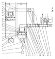
- Fig. 1 a first embodiment of the inventive device for feeding auxiliary equipment for a fuel-electric vehicle is shown.
- the device according to the invention Fig. 1 includes an internal combustion engine 1, a driven by the internal combustion engine 1 generator 2 and a voltage side connected to the generator 2 and the generator 2 associated rectifier 3, the rectifier 3 on the DC side with a first and a second terminal 5, 6 of the rectifier 3 and the rectifier 3 downstream DC voltage circuit 4 is connected.
- a first and a second buck converter 7, 8 are provided, the first and the second buck converter 7, 8 being respectively connected to the first and second terminals 5, 6 of the DC voltage circuit 4.
- Fig. 1 includes an internal combustion engine 1, a driven by the internal combustion engine 1 generator 2 and a voltage side connected to the generator 2 and the generator 2 associated rectifier 3, the rectifier 3 on the DC side with a first and a second terminal 5, 6 of the rectifier 3 and the rectifier 3 downstream DC voltage circuit 4 is connected.
- a first and a second buck converter 7, 8 are provided, the first and
- FIG. 1 represents the DC voltage circuit 4 with respect to the first and second buck converter 7, 8 in particular a common DC voltage circuit 4, wherein in particular the first and second buck converter 7, 8 is connected downstream of the DC voltage circuit 4. Furthermore, the first and second buck converters 7, 8 are connected to a common DC voltage bus 9 downstream of the first and second buck converters 7, 8 for supplying the auxiliary power equipment 10.
- Fig. 1 Inverter of auxiliary equipment 10 and / or DC voltage adjuster of the auxiliary operating devices 10 connected to the power supply.
- the voltage at the DC busbar 9 can be set with advantage. This setting is made such that the voltage at the DC voltage busbar 9 is lower than the voltage between the first and second terminals of the 5, 6 DC voltage circuit 4. Due to the lower compared to the DC voltage circuit 4 voltage of the DC busbar 9, the isolation distance of the busbars of the DC busbar 9, can be reduced, so that advantageously space can be saved and also the assembly and maintenance costs can be kept low or minimized. Furthermore, a redundant supply of DC voltage busbar 9 is possible by the two connected to the common DC voltage bus 9 buck converter 7, 8.
- the inventive device is characterized very robust, insensitive to interference and is characterized by a high availability.
- Fig. 1 is the respective buck converter 7, 8 formed by a series circuit of a drivable power semiconductor switch 11 with a diode 12 and by a parallel to the series circuit of the drivable power semiconductor switch 11 connected to the diode 12 capacitance 13.
- the controllable power semiconductor switch 11 is formed as a bipolar transistor with insulated gate electrode (IGBT).
- IGBT turn-off thyristor
- IGCT - Integrated Gate Commutated Thyristor an integrated thyristor with commutated drive electrode
- the controllable power semiconductor switch 11 is furthermore connected to the first terminal 5 of the DC voltage circuit 4 and the diode 12 is connected to the second terminal 6 of the DC voltage circuit 4.
- the diode 12 through a first connection 14 and the connection point of the diode 12 with the drivable power semiconductor switch 11 through a second connection 15 with the common DC busbar 9 connected.
- the respective buck converter 7, 8 thus comes with a minimum number of components and is thus very simple and space-saving feasible. Due to the small number of components of the first and second buck converter 7, 8 is particularly robust and resistant to interference and therefore has a high availability.
- a filter circuit 16 advantageously effects that unwanted voltage oscillations and current oscillations generated by switching operations of the respective buck converter 7, 8 are filtered out, so that the voltage of the DC busbar 9, ie the voltage present between the busbars, is almost a DC voltage.
- a second embodiment of the inventive device according to Fig. 2 is in contrast to the first embodiment according to Fig. 1 in the respective buck converter 7, 8 in the first connection 14 and in the second connection 15 each have a current direction limiting element 17 is turned on.
- the respective current-direction limiting element 17 serves to ensure that only one current flows in a defined current direction from the respective buck converter 7, 8 back to the DC voltage bus 9 and back again. This advantageously prevents a fault current, for example caused by faults in the DC busbar 9 and / or a fault in one or more auxiliary operating devices 10, from flowing back to the respective buck converter 7, 8 and causing damage or even destruction to the respective buck converter 7, 8.
- the respective current direction limiting element 17 is according to Fig. 2 preferably designed as a diode and thus advantageously very simple and space-saving feasible.
- a third embodiment of the inventive device according to Fig. 3 is different from the first and second embodiments Fig. 1 and Fig. 2 the respective buck converter 7, 8 by a first and a second series circuit 7a, 7b, 8a, 8b each of a controllable power semiconductor switch 11 a, 11 b formed with a diode 12a, 12b and by a parallel connected to each series circuit capacitance 13, wherein the Diode 12a of the first series circuit 7a, 8a is connected to the diode 12b of the second series circuit 7b, 8b.
- the controllable power semiconductor switch 11 a, 11 b as a bipolar transistor with insulated gate electrode (IGBT) is formed.
- IGBT insulated gate electrode
- controllable power semiconductor switch is designed as a power MOSFET, as a turn-off thyristor (GTO) or as an integrated thyristor with commutated drive electrode (IGCT - Integrated Gate Commutated Thyristor).
- GTO turn-off thyristor
- IGCT - Integrated Gate Commutated Thyristor an integrated thyristor with commutated drive electrode
- connection point of the diode 12a of the first series circuit 7a, 8a to the drivable power semiconductor switch 11a of the first series circuit 7a, 8a is connected to the common DC voltage bus 9 through a first connection 14.
- connection point of the diode 12b of the second series circuit 7b, 8b with the drivable power semiconductor switch 11b of the second series circuit 7b, 8b connected by a second connection 15 to the common DC busbar 9.
- the respective buck converter 7, 8 according to Fig. 3 also comes with a minimum number of components and is thus very simple and space-saving feasible. Due to the small number of components of the first and second buck converter 7, 8 is particularly robust and resistant to interference and therefore has a high availability.
- Fig. 3 is connected to the respective buck converter 7, 8 between the first connection 14 and the common DC voltage bus 9 and between the second connection 15 and the common DC voltage bus 9, a filter circuit 16.
- the filter circuit 16 advantageously effects that unwanted voltage oscillations and current oscillations generated by switching operations of the respective buck converter 7, 8 are filtered out, so that the voltage of the DC busbar 9, ie the voltage present between the busbars, is almost a DC voltage.
- a fourth embodiment of the inventive device according to Fig. 4 is different from the third embodiment according to Fig. 3 in the respective buck converter 7, 8 in the first connection 14 and in the second connection 15 each have a current direction limiting element 17 is turned on.
- the respective current-direction limiting element 17 serves to ensure that only one current flows in a defined current direction from the respective buck converter 7, 8 back to the DC voltage bus 9 and back again. This advantageously prevents a fault current, for example caused by a fault of the DC voltage bus 9 and / or an error in one or more auxiliary operation devices 10, from flowing back to the respective buck converter 7, 8 and damaging or even destroying the respective buck converter 7, 8 ,
- the respective current direction limiting element 17 is according to Fig. 4 preferably designed as a diode and thus advantageously very simple and space-saving feasible.
- a fifth and sixth embodiment of the inventive device according to Fig. 5 and Fig. 6 is alternative to the first, second, third and fourth embodiment according to Fig. 1 . Fig. 2 . Fig. 3 and Fig. 4 instead of the second buck converter 8, a further AC voltage side connected to the generator 2 rectifier 21 is provided, wherein the first buck converter 7 and another AC voltage side connected to the generator 2 and the generator 2 associated rectifier 21 with a first buck converter 7 and the other rectifier 21 downstream common DC voltage bus 9 is connected to the supply of auxiliary equipment 10.
- the first buck converter 7 in particular the DC voltage circuit 4 downstream.
- the first buck converter 7 is after Fig. 5 corresponding the first buck converter after Fig.
- the voltage at the DC voltage busbar 9 can be set with advantage. This setting is made such that the voltage at the DC voltage busbar 9 is lower than the voltage between the first and second terminals of the 5, 6 DC voltage circuit 4. Due to the lower compared to the DC voltage circuit 4 voltage of the DC busbar 9, the isolation distance of the busbars of the DC busbar 9, can be reduced, so that advantageously space can be saved and also the assembly and maintenance costs can be kept low or minimized. Furthermore, by the first buck converter 7 and the other rectifier 21, which are both connected to the common DC voltage bus 9, a redundant power supply of the DC busbar 9 possible.
- the power supply of the DC voltage bus 9 is effected via the further rectifier 21, so that the auxiliary power devices 10 can continue to be supplied via their inverters and / or DC voltage actuators.
- the inventive device is characterized very robust, insensitive to interference and is characterized by a high availability.
- Fig. 5 and Fig. 6 is in the further rectifier 21, as well as the first buck converter 7, in the first connection 14 and in the second connection 15 each have a current direction limiting element 17 is turned on.
- the respective current-direction limiting element 17 serves to ensure that only one current flows in a defined current direction from the first buck converter 7 or from the further rectifier 21 to the DC voltage bus 9 and back again. This advantageously prevents a fault current, for example caused by a fault of the DC voltage bus 9 and / or an error in one or more auxiliary operation devices 10, from flowing back to the first buck converter 7 or to the further rectifier 21 and the first buck converter 7 or the other Rectifier 21 damaged or even destroyed.
- the respective current direction limiting element 17 is according to Fig. 5 and Fig. 6 preferably designed as a diode and thus advantageously very simple and space-saving feasible.
- the separating element 20 is preferably designed as a low-inductance switch, for example as a mechanical or as a controllable power semiconductor switch, or as a fuse.
- the common DC voltage bus 9 has an overvoltage limiting network 18.
- the overvoltage limiting network 18 is formed by a resistor and a controllable switch, preferably a controllable power semiconductor switch, wherein the overvoltage limiting network 18 is actuated by closing the switch at an occurring overvoltage of the voltage of the DC busbar 9.
- the overvoltage limiting network 18 is actuated for a predetermined period of time. This period of time is preferably predetermined as a function of the thermal capacity of the resistor. The operation is carried out according to known to the expert criteria, which will not be discussed in detail at this point.
- a separator 20 is turned on. This advantageously ensures that the disturbed or failed buck converter 7, 8, the associated first and second connection 14, 15, for example, does not short-circuit.
- the separating element 20 is preferably low inductive Switch, designed for example as a mechanical or as a controllable power semiconductor switch, or as a backup.
- Fig. 7 . Fig. 8 . Fig. 9 and Fig. 10 are alternative to the first, second, third, fourth, fifth and sixth embodiments according to Fig. 1 . Fig. 2 . Fig. 3 . Fig. 4 . Fig. 5 and Fig.
- first and second rectifiers 3a, 3b are connected to the generator 2 on the alternating voltage side, the first rectifier 3a having a first and a second terminal 5a, 6a of the first rectifier 3a and the first rectifier circuit 3a connected downstream of the first rectifier 3a and the second rectifier 3b on the DC side with a first and a second terminal 5b, 6b of the second rectifier 3b associated and the second rectifier 3b downstream second DC voltage circuit 4b is connected.
- a first and a second buck converter 7, 8 is provided, wherein the first buck converter 7 to the first and second terminals 5a, 6a of the first DC voltage circuit 4a and the second buck converter 8 to the first and second terminals 5b, 6b of the second DC voltage circuit 4b connected is. Furthermore, the first and second buck converters 7, 8 are connected to a common DC voltage bus 9 downstream of the first and second buck converters 7, 8 for supplying the auxiliary power equipment 10. According to FIGS. 7 to 10 the first buck converter 7 is followed in particular by the first DC voltage circuit 4a and the second buck converter 8 in particular is connected downstream of the second DC voltage circuit 4b. According to Fig. 7 . Fig. 8 . Fig. 9 and Fig.
- Fig. 10 has the common DC voltage busbar 9 two of the busbars.
- To the common DC voltage busbar 9 are according to Fig. 7 . Fig. 8 .
- Fig. 9 and Fig. 10 Inverter of the auxiliary equipment 10 and / or DC voltage adjuster of the auxiliary equipment 10 connected to the power supply.
- the voltage at the DC busbar 9 can be set with advantage. This setting is made such that the voltage at the DC voltage busbar 9 is lower than the voltage between the first and second terminals 5a, 5b, 6a, 6b of the respective DC voltage circuit 4a, 4b.
- the isolation distance of the busbar strands of the DC busbar 9 can be reduced, so that advantageously space can be saved and also the assembly and maintenance costs can be kept low or minimized.
- a redundant supply of DC voltage busbar 9 is possible by the two connected to the common DC voltage bus 9 buck converter 7, 8.
- the DC voltage busbar 9 is fed via the second buck converter 8, so that the auxiliary power equipment 10 can continue to be supplied via its inverters and / or DC voltage actuators.
- the device is therefore very robust, insensitive to interference and characterized by a high availability.
- Fig. 7 . Fig. 8 . Fig. 9 and Fig. 10 is the respective buck converter 7, 8 formed by a series circuit of a drivable power semiconductor switch 11 with a diode 12 and by a parallel to the series circuit of the drivable power semiconductor switch 11 connected to the diode 12 capacitance 13.
- the controllable power semiconductor switch 11 is formed as a bipolar transistor with insulated gate electrode (IGBT).
- controllable power semiconductor switch is designed as a power MOSFET, as a turn-off thyristor (GTO) or as an integrated thyristor with commutated drive electrode (IGCT - Integrated Gate Commutated Thyristor).
- GTO turn-off thyristor
- IGCT - Integrated Gate Commutated Thyristor IGCT - Integrated Gate Commutated Thyristor
- the diode 12 is connected by a first connection 14 and the connection point of the diode 12 to the controllable power semiconductor switch 11 by a second connection 15 to the common DC voltage busbar 9.
- the respective buck converter 7, 8 thus comes with a minimum number of components and is thus very simple and space-saving feasible. Due to the small number of components of the first and second buck converter 7, 8 is particularly robust and resistant to interference and therefore has a high availability.
- the filter circuit 16 advantageously effects that unwanted voltage oscillations and current oscillations generated by switching operations of the respective buck converter 7, 8 are filtered out, so that the voltage of the DC busbar 9, ie the voltage present between the busbars, is almost a DC voltage.
- the eighth embodiment of the device according to Fig. 8 is in contrast to the seventh embodiment according to Fig. 7 in the respective buck converter 7, 8 in the first connection 14 and in the second connection 15 each have a current direction limiting element 17 is turned on.
- the respective current-direction limiting element 17 serves to ensure that only one current flows in a defined current direction from the respective buck converter 7, 8 back to the DC voltage bus 9 and back again. This advantageously prevents a fault current, for example caused by faults in the DC busbar 9 and / or a fault in one or more auxiliary operating devices 10, from flowing back to the respective buck converter 7, 8 and causing damage or even destruction to the respective buck converter 7, 8.
- the respective current direction limiting element 17 is according to Fig. 8 preferably designed as a diode and thus advantageously very simple and space-saving feasible.
- the respective step-down converter 7, 8 by a first and a second series circuit 7a, 7b, 8a, 8b each of a controllable power semiconductor switch 11a, 11b formed with a diode 12a, 12b and by a respective parallel connected to each series circuit capacitance 13, wherein the diode 12a of the first series circuit 7a, 8a is connected to the diode 12b of the second series circuit 7b, 8b.
- the controllable power semiconductor switch 11a, 11b is formed as a bipolar transistor with insulated gate electrode (IGBT).
- controllable power semiconductor switch is designed as a power MOSFET, as a turn-off thyristor (GTO) or as an integrated thyristor with commutated drive electrode (IGCT - Integrated Gate Commutated Thyristor).
- GTO turn-off thyristor
- IGCT - Integrated Gate Commutated Thyristor an integrated thyristor with commutated drive electrode
- the respective buck converter 7, 8 according to Fig. 9 also comes with a minimum number of components and is thus very simple and space-saving feasible. Due to the small number of components of the first and second buck converter 7, 8 is particularly robust and resistant to interference and therefore has a high availability.
- Fig. 9 is connected to the respective buck converter 7, 8 between the first connection 14 and the common DC voltage bus 9 and between the second connection 15 and the common DC voltage bus 9, a filter circuit 16.
- the filter circuit 16 advantageously causes by switching operations of the respective Tiefsetzstellers 7, 8 generated unwanted voltage oscillations and current oscillations are filtered out, so that the voltage of the DC busbar 9, ie, the voltage applied between the busbars, voltage is almost a DC voltage.
- the tenth embodiment of the device according to Fig. 10 is in contrast to the ninth embodiment according to Fig. 9 in the respective buck converter 7, 8 in the first connection 14 and in the second connection 15 each have a current direction limiting element 17 is turned on.
- the respective current-direction limiting element 17 serves to ensure that only one current flows in a defined current direction from the respective buck converter 7, 8 back to the DC voltage bus 9 and back again. This advantageously prevents a fault current, for example caused by a fault of the DC voltage bus 9 and / or an error in one or more auxiliary operation devices 10, from flowing back to the respective buck converter 7, 8 and damaging or even destroying the respective buck converter 7, 8 ,
- the respective current direction limiting element 17 is according to Fig. 10 preferably designed as a diode and thus advantageously very simple and space-saving feasible.
- the common DC voltage bus 9 has an overvoltage limiting network 18.
- the overvoltage limiting network 18 is formed by a resistor and a controllable switch, preferably a controllable power semiconductor switch, wherein the overvoltage limiting network 18 is actuated by closing the switch at an occurring overvoltage of the voltage of the DC busbar 9.
- the overvoltage limiting network 18 is actuated for a predetermined period of time. This period of time is preferably predetermined as a function of the thermal capacity of the resistor. The operation is carried out according to known to the expert criteria, which will not be discussed in detail at this point.
- a separator 20 is turned on. This advantageously ensures that the disturbed or failed buck converter 7, 8, the associated first and second connection 14, 15, for example, does not short-circuit.
- the separating element 20 is preferably designed as a low-inductance switch, for example as a mechanical or as a controllable power semiconductor switch, or as a fuse.
Description
Die Erfindung bezieht sich auf das Gebiet der Hilfsbetriebeeinrichtungen für kraftstoffelektrisch angetriebene Fahrzeuge. Sie geht aus von einer Vorrichtung zur Speisung von Hilfsbetriebeeinrichtungen für ein kraftstoffelektrisch angetriebenes Fahrzeug gemäss dem Oberbegriff der unabhängigen Ansprüche.The invention relates to the field of auxiliary equipment for fuel-electrically driven vehicles. It is based on a device for feeding auxiliary equipment for a fuel-electrically driven vehicle according to the preamble of the independent claims.
Hilfsbetriebeeinrichtungen für kraftstoffelektrisch angetriebene Fahrzeuge werden heute hauptsächlich in diesel-elektrischen Lokomotiven oder grossen diesel-elektrischen Minenfahrzeugen eingesetzt, wobei die Hilfsbetriebeeinrichtungen, als Lüfter, Klimaanlagen, Stellmotoren, Bordnetzumrichter usw, ausgebildet sind. Solche Hilfsbetriebeeinrichtungen werden gängigerweise mittels einer geeigneten Vorrichtung gespeist. Eine solche Vorrichtung zur Speisung von Hilfsbetriebeeinrichtungen für ein kraftstoffelektrisch angetriebenes Fahrzeug ist beispielsweise in der
Selbstverständlich ist es auch denkbar, dass ein zweiter wechselspannungsseitig mit dem Generator verbundener Gleichrichter vorgesehen ist. Der zweite Gleichrichter ist dann gleichspannungsseitig mit einem ersten und einem zweiten Anschluss eines zweiten Gleichspannungskreises verbunden, wobei ein zweiter Antriebswechselrichter an den ersten und zweiten Anschluss des zweiten Gleichspannungskreises angeschlossen ist, welcher zweite Antriebswechselrichter wechselspannungsseitig einen oder mehrere Fahrmotoren des Fahrzeugs speist.Of course, it is also conceivable that a second AC side connected to the generator rectifier is provided. The second rectifier is then connected on the DC voltage side to a first and a second terminal of a second DC voltage circuit, wherein a second drive inverter is connected to the first and second terminals of the second DC voltage circuit, which second drive inverter feeds one or more traction motors of the vehicle on the AC voltage side.
Da der Leistungsbedarf solcher Fahrmotoren sehr gross ist, liegt zwischen dem ersten und zweiten Anschluss des Gleichspannungskreises typischerweise eine Gleichspannung von mehreren Kilovolt an, um die entsprechende Leistung bereitstellen zu können. Problematisch bei der Vorrichtung zur Speisung von Hilfsbetriebeeinrichtungen für ein kraftstoffelektrisch angetriebenes Fahrzeug der
In der
Aufgabe der Erfindung ist es deshalb, eine Vorrichtung zur Speisung von Hilfsbetriebeeinrichtungen für ein kraftstoffelektrisch angetriebenes Fahrzeug anzugeben, welche einen geringen Platzbedarf aufweist und zudem robust und störungsunempfindlich ist. Diese Aufgabe wird durch die Merkmale des Anspruchs 1 beziehungsweise des Anspruchs 2 gelöst. In den abhängigen Ansprüchen sind vorteilhafte Weiterbildungen der Erfindung angegeben.The object of the invention is therefore to provide a device for feeding auxiliary equipment for a fuel-electrically driven vehicle, which has a small footprint and is also robust and insensitive to interference. This object is solved by the features of
Die erfindungsgemässe Vorrichtung zur Speisung von Hilfsbetriebeeinrichtungen für ein kraftstoffelektrisch angetriebenes Fahrzeug umfasst eine Brennkraftmaschine, einen von der Brennkraftmaschine angetriebenen einzigen Generator und einen wechselspannungsseitig mit dem Generator verbundenen und dem Generator zugeordneten einzigen Gleichrichter, wobei der Gleichrichter gleichspannungsseitig mit einem ersten und einem zweiten Anschluss eines dem Gleichrichter zugeordneten und dem Gleichrichter nachgeschalteten einzigen Gleichspannungskreises verbunden ist. Erfindungsgemäss ist ein erster und ein zweiter Tiefsetzsteller vorgesehen, wobei der erste und zweite Tiefsetzsteller jeweils mit dem ersten und zweiten Anschluss des Gleichspannungskreises verbunden ist und der erste und zweite Tiefsetzsteller ferner mit einer dem ersten und zweiten Tiefsetzsteller nachgeschalteten gemeinsamen Gleichspannungsverschienung zur Speisung der Hilfsbetriebeeinrichtungen verbunden ist. An die gemeinsame Gleichspannungsverschienung sind Wechselrichter der Hilfsbetriebeeinrichtungen und/oder Gleichspannungsteller der Hilfsbetriebeinrichtungen zu deren Speisung angeschlossen.The inventive device for feeding auxiliary equipment for a fuel-electrically driven vehicle comprises an internal combustion engine, a single generator driven by the internal combustion engine and an alternating voltage side connected to the generator and the generator associated with the single rectifier, wherein the rectifier is connected on the DC side with a first and a second terminal of a rectifier associated and the rectifier downstream single DC voltage circuit. According to the invention a first and a second buck converter is provided, wherein the first and second buck converter is connected to the first and second terminal of the DC circuit and the first and second buck converter is further connected to the first and second buck converter downstream common DC bus for feeding the auxiliary equipment , To the common DC voltage bus inverter of the auxiliary equipment and / or DC voltage controller of the auxiliary equipment are connected to the power supply.
Durch die beiden Tiefsetzsteller kann die Spannung an der Gleichspannungsverschienung mit Vorteil eingestellt werden. Diese Einstellung erfolgt derart, dass die Spannung an der Gleichspannungsverschienung tiefer ist, als die Spannung zwischen dem ersten und zweiten Anschluss des Gleichspannungskreises. Mittels der im Vergleich zum Gleichspannungskreis niedrigeren Spannung der Gleichspannungsverschienung kann der Isolationsabstand der Gleichspannungsverschienung, d.h. der Verschienungsstränge der Gleichspannungsverschienung, verringert werden, so dass mit Vorteil Platz gespart werden kann und zudem der Montage- und Wartungsaufwand gering gehalten werden kann. Weiterhin ist durch die beiden mit der gemeinsamen Gleichspannungsverschienung verbundenen Tiefsetzsteller eine redundante Speisung der Gleichspannungsverschienung möglich, d.h. bei einer Störung oder einem Ausfall eines Tiefsetzstellers erfolgt die Speisung der Gleichspannungsverschienung über den anderen Tiefsetzsteller, so dass die Hilfsbetriebeeinrichtungen über ihre Wechselrichter und/oder Gleichspannungsteller weiter gespeist werden können. Die erfindungsgemässe Vorrichtung ist dadurch sehr robust, störungsunempfindlich und zeichnet sich durch eine hohe Verfügbarkeit aus.Due to the two buck converters, the voltage at the DC busbar can be set with advantage. This setting is made such that the voltage at the DC busbar is lower than the voltage between the first and second terminals of the DC voltage circuit. By means of the voltage of the DC busbar, which is lower than that of the DC voltage circuit, the insulation distance of the DC busbar, i. the busbars of the DC busbar, be reduced, so that advantageously can be saved space and also the assembly and maintenance costs can be kept low. Furthermore, a redundant supply of DC voltage busbar is possible by the two connected to the common DC voltage buck converter bucking, i. in the event of a fault or a failure of a step-down converter, the DC voltage supply is fed via the other step-down converter, so that the auxiliary device devices can continue to be supplied via their inverters and / or DC voltage controllers. The inventive device is characterized very robust, insensitive to interference and is characterized by a high availability.
Mittels der im Vergleich zum Gleichspannungskreis niedrigeren Spannung der Gleichspannungsverschienung müssen beispielsweise die Wechselrichter und/oder Gleichspannungsteller der Hilfsbetriebeeinrichtungen, d.h. die Leistungshalbleiterschalter der Wechselrichter und/oder Gleichspannungsteller mit zugehörigen Schutzeinrichtungen und Betriebsverfahren, nicht, wie aus dem Stand der Technik bekannt, auf die hohe Spannung des Gleichspannungskreises ausgelegt sein, sondern lediglich auf die niedrigere Spannung der Gleichspannungsverschienung. Vorteilhaft vereinfacht sich dadurch der Aufbau der Wechselrichter und/oder Gleichspannungsteller, die Wechselrichter und/oder Gleichspannungsteller sind störungsunempfindlicher und benötigen entsprechend wenig Platz. Zudem bewirkt der einfache und platzsparende Aufbau der Wechselrichter und/oder Gleichspannungsteller einen geringen Montage- und Wartungsaufwand.By means of the voltage of the DC voltage busbar, which is lower in comparison to the DC voltage circuit, the inverters and / or DC voltage adjusters of the auxiliary operating devices, ie the power semiconductor switches of the inverters and / or DC voltage adjusters with associated protective devices and operating methods, do not have to withstand the high voltage as known from the prior art of the DC circuit be designed, but only to the lower voltage of the DC busbar. Advantageously, thereby simplifying the structure of the inverter and / or DC voltage controller, the inverter and / or DC voltage controller are less sensitive to interference and require correspondingly little space. In addition, the simple and space-saving design of the inverter and / or DC voltage controller causes low installation and maintenance costs.
Alternativ zu dem zweiten Tiefsetzsteller ist ein weiterer wechselspannungsseitig mit dem einzigen Generator verbundener und dem Generator zugeordneter Gleichrichter vorgesehen, wobei der erste Tiefsetzsteller und der weitere Gleichrichter mit einer dem ersten Tiefsetzsteller und dem weiteren Gleichrichter nachgeschalteten gemeinsamen Gleichspannungsverschienung zur Speisung der Hilfsbetriebeeinrichtungen verbunden ist.As an alternative to the second buck converter, a further AC voltage side connected to the single generator and the generator associated rectifier is provided, wherein the first buck converter and the further rectifier is connected to a the first buck converter and the other rectifier downstream common DC bus for feeding the auxiliary equipment.
Durch den ersten Tiefsetzsteller und den weiteren Gleichrichter kann ebenfalls die Spannung an der Gleichspannungsverschienung mit Vorteil eingestellt werden, wie dies bei der Lösung mit zwei Tiefsetzstellern bereits erläutert wurde. Mittels der im Vergleich zum Gleichspannungskreis erreichten niedrigeren Spannung der Gleichspannungsverschienung kann der Isolationsabstand der Gleichspannungsverschienung, d.h. der Verschienungsstränge der Gleichspannungsverschienung, verringert werden, so dass mit Vorteil Platz gespart werden kann und zudem der Montage- und Wartungsaufwand gering gehalten werden kann. Weiterhin ist durch den ersten Tiefsetzsteller und den weiteren Gleichrichter, welche beide mit der gemeinsamen Gleichspannungsverschienung verbunden sind, eine redundante Speisung der Gleichspannungsverschienung möglich, d.h. bei einer Störung oder einem Ausfall beispielsweise des Tiefsetzstellers erfolgt die Speisung der Gleichspannungsverschienung über den Gleichrichter, so dass die Hilfsbetriebeeinrichtungen über ihre Wechselrichter und/oder Gleichspannungsteller weiter gespeist werden können. Die erfindungsgemässe Vorrichtung ist dadurch sehr robust, störungsunempfindlich und zeichnet sich durch eine hohe Verfügbarkeit aus.By the first step-down converter and the other rectifier, the voltage at the DC voltage busbar can also be set with advantage, as has already been explained in the solution with two buck converters. By means of the lower voltage of the DC busbar compared to the DC voltage circuit, the isolation distance of the DC busbar, i. the busbars of the DC busbar, be reduced, so that advantageously can be saved space and also the assembly and maintenance costs can be kept low. Furthermore, by the first step-down converter and the other rectifier, which are both connected to the common DC voltage busbar, a redundant supply of DC busbars possible, i. in the case of a fault or a failure of, for example, the buck-converter, the DC voltage supply is fed via the rectifier, so that the auxiliary equipment can continue to be supplied via its inverters and / or DC voltage controllers. The inventive device is characterized very robust, insensitive to interference and is characterized by a high availability.
Auch bei der alternativen Lösung mit dem ersten Tiefsetzsteller und dem weiteren Gleichrichter müssen beispielsweise die Wechselrichter und/oder Gleichspannungsteller der Hilfsbetriebeeinrichtungen aufgrund der im Vergleich zum Gleichspannungskreis niedrigeren Spannung der Gleichspannungsverschienung nicht, wie aus dem Stand der Technik bekannt, auf die hohe Spannung des Gleichspannungskreises ausgelegt sein, sondern lediglich auf die niedrigere Spannung der Gleichspannungsverschienung. Vorteilhaft vereinfacht sich dadurch der Aufbau der Wechselrichter und/oder Gleichspannungsteller, die Wechselrichter und/oder Gleichspannungsteller sind störungsunempfindlicher und benötigen entsprechend wenig Platz. Zudem bewirkt der einfache und platzsparende Aufbau der Wechselrichter und/oder Gleichspannungsteller einen geringen Montage- und Wartungsaufwand.Even in the alternative solution with the first step-down converter and the further rectifier, for example, the inverters and / or DC voltage adjusters of the auxiliary operating devices do not have to be, as known from the prior art, due to the lower voltage of the DC busbar compared to the DC voltage circuit. be designed for the high voltage of the DC circuit, but only to the lower voltage of the DC busbar. Advantageously, thereby simplifying the structure of the inverter and / or DC voltage controller, the inverter and / or DC voltage controller are less sensitive to interference and require correspondingly little space. In addition, the simple and space-saving design of the inverter and / or DC voltage controller causes low installation and maintenance costs.
Diese und weitere Aufgaben, Vorteile und Merkmale der vorliegenden Erfindung werden aus der nachfolgenden detaillierten Beschreibung bevorzugter Ausführungsformen der Erfindung in Verbindung mit der Zeichnung offensichtlich.These and other objects, advantages and features of the present invention will become more apparent from the following detailed description of preferred embodiments of the invention taken in conjunction with the accompanying drawings.
Es zeigen:
- Fig. 1
- eine erste Ausführungsform einer erfindungsgemässen Vorrichtung zur Spei- sung von Hilfsbetriebeeinrichtungen für ein kraftstoffelektrisch angetriebenes Fahrzeug,
- Fig. 2
- eine zweite Ausführungsform der erfindungsgemässen Vorrichtung,
- Fig. 3
- eine dritte Ausführungsform der erfindungsgemässen Vorrichtung,
- Fig. 4
- eine vierte Ausführungsform der erfindungsgemässen Vorrichtung,
- Fig. 5
- eine fünfte Ausführungsform der erfindungsgemässen Vorrichtung,
- Fig. 6
- eine sechste Ausführungsform der erfindungsgemässen Vorrichtung,
- Fig. 7
- eine siebte Ausführungsform einer nicht erfindungsgemässen Vorrichtung,
- Fig. 8
- eine achte Ausführungsform einer nicht erfindungsgemässen Vorrichtung,
- Fig. 9
- eine neunte Ausführungsform einer nicht erfindungsgemässen Vorrichtung und
- Fig. 10
- eine zehnte Ausführungsform einer nicht erfindungsgemässen Vorrichtung.
- Fig. 1
- A first embodiment of a device according to the invention for supplying auxiliary equipment for a fuel-electric vehicle,
- Fig. 2
- A second embodiment of the device according to the invention,
- Fig. 3
- A third embodiment of the device according to the invention,
- Fig. 4
- A fourth embodiment of the device according to the invention,
- Fig. 5
- A fifth embodiment of the device according to the invention,
- Fig. 6
- A sixth embodiment of the device according to the invention,
- Fig. 7
- A seventh embodiment of a device not according to the invention,
- Fig. 8
- an eighth embodiment of a device not according to the invention,
- Fig. 9
- A ninth embodiment of a non-inventive device and
- Fig. 10
- A tenth embodiment of a device not according to the invention.
Die in der Zeichnung verwendeten Bezugszeichen und deren Bedeutung sind in der Bezugszeichenliste zusammengefasst aufgelistet. Grundsätzlich sind in den Figuren gleiche Teile mit gleichen Bezugszeichen versehen. Die beschriebenen Ausführungsformen stehen beispielhaft für den Erfindungsgegenstand und haben keine beschränkende Wirkung.The reference numerals used in the drawings and their meaning are listed in the list of reference numerals. Basically, the same parts are provided with the same reference numerals in the figures. The described embodiments are exemplary of the subject invention and have no limiting effect.
In
Durch die beiden Tiefsetzsteller 7, 8 kann die Spannung an der Gleichspannungsverschienung 9 mit Vorteil eingestellt werden. Diese Einstellung erfolgt derart, dass die Spannung an der Gleichspannungsverschienung 9 tiefer ist, als die Spannung zwischen dem ersten und zweiten Anschluss des 5, 6 Gleichspannungskreises 4. Durch die im Vergleich zum Gleichspannungskreis 4 niedrigeren Spannung der Gleichspannungsverschienung 9 kann der Isolationsabstand der Verschienungsstränge der Gleichspannungsverschienung 9, verringert werden, so dass vorteilhaft Platz gespart werden kann und zudem der Montage- und Wartungsaufwand gering gehalten beziehungsweise minimiert werden kann. Weiterhin ist durch die beiden mit der gemeinsamen Gleichspannungsverschienung 9 verbundenen Tiefsetzsteller 7, 8 eine redundante Speisung der Gleichspannungsverschienung 9 möglich. Dies bedeutet, dass bei einer Störung oder einem Ausfall beispielsweise des ersten Tiefsetzstellers 7 die Speisung der Gleichspannungsverschienung 9 über den zweiten Tiefsetzsteller 8 erfolgt, so dass die Hilfsbetriebeeinrichtungen 10 über ihre Wechselrichter und/oder Gleichspannungsteller weiter gespeist werden können. Die erfindungsgemässe Vorrichtung ist dadurch sehr robust, störungsunempfindlich und zeichnet sich durch eine hohe Verfügbarkeit aus.By the two
Gemäss
Gemäss
In einer zweiten Ausführungsform der erfindungsgemässen Vorrichtung gemäss
In einer dritten Ausführungsform der erfindungsgemässen Vorrichtung gemäss
Gemäss
In einer vierten Ausführungsform der erfindungsgemässen Vorrichtung gemäss
In einer fünften und sechsten Ausführungsform der erfindungsgemässen Vorrichtung nach
Durch den ersten Tiefsetzsteller 7 und dem weiteren Gleichrichter 21 kann die Spannung an der Gleichspannungsverschienung 9 mit Vorteil eingestellt werden. Diese Einstellung erfolgt derart, dass die Spannung an der Gleichspannungsverschienung 9 tiefer ist, als die Spannung zwischen dem ersten und zweiten Anschluss des 5, 6 Gleichspannungskreises 4. Durch die im Vergleich zum Gleichspannungskreis 4 niedrigeren Spannung der Gleichspannungsverschienung 9 kann der Isolationsabstand der Verschienungsstränge der Gleichspannungsverschienung 9, verringert werden, so dass vorteilhaft Platz gespart werden kann und zudem der Montage- und Wartungsaufwand gering gehalten beziehungsweise minimiert werden kann. Ferner ist durch die den ersten Tiefsetzsteller 7 und den weiteren Gleichrichter 21, welche beide mit der gemeinsamen Gleichspannungsverschienung 9 verbunden sind, eine redundante Speisung der Gleichspannungsverschienung 9 möglich. Dies bedeutet, dass bei einer Störung oder einem Ausfall beispielsweise des ersten Tiefsetzstellers 7 die Speisung der Gleichspannungsverschienung 9 über den weiteren Gleichrichter 21 erfolgt, so dass die Hilfsbetriebeeinrichtungen 10 über ihre Wechselrichter und/oder Gleichspannungsteller weiter gespeist werden können. Die erfindungsgemässe Vorrichtung ist dadurch sehr robust, störungsunempfindlich und zeichnet sich durch eine hohe Verfügbarkeit aus.By the
Gemäss
Zur Abtrennung des, wie vorstehend erwähnt, gestörten oder ausgefallenen ersten Tiefsetzstellers 7 oder des weiteren Gleichrichters 21 ist gemäss
Bei sämtlichen Ausführungsformen der erfindungsgemässen Vorrichtung nach
Zur Abtrennung eines, wie vorstehend erwähnt, gestörten oder ausgefallenen Tiefsetzstellers 7, 8 ist bei den Ausführungsformen der erfindungsgemässen Vorrichtung nach
In einer siebten, achten, neunten und zehnten Ausführungsform der Vorrichtung nach
Durch die beiden Tiefsetzsteller 7, 8 gemäss
Gemäss
Gemäss
In der achten Ausführungsform der Vorrichtung gemäss
In der neunten Ausführungsform der Vorrichtung gemäss
Gemäss
In der zehnten Ausführungsform der Vorrichtung gemäss
Bei sämtlichen Ausführungsformen der Vorrichtung nach
Zur Abtrennung eines, wie vorstehend erwähnt, gestörten oder ausgefallenen Tiefsetzstellers 7, 8 ist bei sämtlichen Ausführungsformen der Vorrichtung nach
- 11
- BrennkraftmaschineInternal combustion engine
- 22
- Generatorgenerator
- 33
- Gleichrichterrectifier
- 3a3a
- erster Gleichrichterfirst rectifier
- 3b3b
- zweiter Gleichrichtersecond rectifier
- 44
- GleichspannungskreisDC circuit
- 4a4a
- erster Gleichspannungskreisfirst DC voltage circuit
- 4b4b
- zweiter Gleichspannungskreissecond DC voltage circuit
- 55
- erster Anschluss des Gleichspannungskreisesfirst connection of the DC voltage circuit
- 5a5a
- erster Anschluss des ersten Gleichspannungskreisesfirst connection of the first DC voltage circuit
- 5b5b
- erster Anschluss des zweiten Gleichspannungskreisesfirst connection of the second DC voltage circuit
- 66
- zweiter Anschluss des Gleichspannungskreisessecond connection of the DC voltage circuit
- 6a6a
- zweiter Anschluss des ersten Gleichspannungskreisessecond connection of the first DC voltage circuit
- 6b6b
- zweiter Anschluss des zweiten Gleichspannungskreisessecond connection of the second DC voltage circuit
- 77
- erster Tiefsetzstellerfirst buck converter
- 7a7a
- erste Serienschaltung des ersten Tiefsetzstellersfirst series connection of the first buck converter
- 7b7b
- zweite Serienschaltung des ersten Tiefsetzstellerssecond series connection of the first buck converter
- 88th
- zweiter Tiefsetzstellersecond buck converter
- 8a8a
- erste Serienschaltung des zweiten Tiefsetzstellersfirst series connection of the second buck converter
- 8b8b
- zweite Serienschaltung des zweiten Tiefsetzstellerssecond series connection of the second buck converter
- 99
- GleichspannungsverschienungDC busbar
- 1010
- HilfsbetriebeeinrichtungenAuxiliary operating devices
- 1111
- ansteuerbarer Leistungshalbleiterschaltercontrollable power semiconductor switch
- 11a11a
- ansteuerbarer Leistungshalbleiterschalter der ersten Serienschaltung des ers- ten und zweiten Tiefsetzstellerscontrollable power semiconductor switch of the first series connection of the first and second buck converter
- 11b11b
- ansteuerbarer Leistungshalbleiterschalter der zweiten Serienschaltung des ersten und zweiten Tiefsetzstellerscontrollable power semiconductor switch of the second series circuit of the first and second buck converter
- 1212
- Diodediode
- 12a12a
- Diode der ersten Serienschaltung des ersten und zweiten TiefsetzstellersDiode of the first series connection of the first and second buck converter
- 12b12b
- Diode der zweiten Serienschaltung des ersten und zweiten TiefsetzstellersDiode of the second series connection of the first and second buck converter
- 1313
- Kapazitätcapacity
- 1414
- erste Verbindungfirst connection
- 1515
- zweite Verbindungsecond connection
- 1616
- Filterschaltungfilter circuit
- 1717
- StromrichtungsbegrenzungselementCurrent direction limiting element
- 1818
- ÜberspannungsbegrenzungsnetzwerksOvervoltage limiting network
- 1919
- Kapazität des ersten SpannungsanstiegsbegrenzungsnetzwerksCapacity of the first voltage rise limiting network
- 2020
- Trennelementseparating element
- 2121
- weiterer Gleichrichteranother rectifier
Claims (14)
- Device for feeding auxiliary operating devices for a fuel/electric vehicle having an internal combustion engine (1), having a single generator (2) which is driven by the internal combustion engine (1), having a single rectifier (3) which is connected on the alternating voltage side to the generator (2) and is assigned to the generator (2), wherein the rectifier (3) is connected on the direct voltage side to a first and a second terminal (5, 6) of a single direct voltage circuit (4) which is assigned to the rectifier (3) and is connected downstream of the rectifier (3),
characterized
in that a first and a second step-down converter (7, 8) are respectively connected to the first and second terminals (5, 6) of the direct voltage circuit (4), and in that the first and second step-down converters (7, 8) are connected to a common direct voltage rail (9), which is connected downstream of the first and second step-down converters (7, 8) and has the purpose of feeding the auxiliary operating devices (10). - Device for feeding auxiliary operating devices for a fuel/electric vehicle having an internal combustion engine (1), having a single generator (2) which is driven by the internal combustion engine (1), having a rectifier (3) which is connected on the alternating voltage side to the generator (2) and is assigned to the generator (2), wherein the rectifier (3) is connected on the direct voltage side to a first and a second terminal (5, 6) of a direct voltage circuit (4) which is assigned to the rectifier (3) and is connected downstream of the rectifier (3), characterized
in that a first step-down converter (7) is connected to the first and second terminals (5, 6) of the direct voltage circuit (4), and
in that the first step-down converter (7) and a further rectifier (21) which is connected on the alternating voltage side to the generator (2) and is assigned to the generator (2) are connected to a common direct voltage rail (9) which is connected downstream of the first step-down converter (7) and the further rectifier (21) and has the purpose of feeding the auxiliary operating devices (10). - Device according to Claim 2, characterized in that the further rectifier (21) is connected to the common direct voltage rail (9) by means of a first connection (14) and by means of a second conenction (15).
- Device according to one of Claims 1 to 3, characterized in that the respective step-down converter (7, 8) is formed by a series circuit of a controllable power semiconductor switch (11) with a diode (12), and by a capacitor (13) which is connected to the diode (12) parallel to the series circuit of the controllable power semiconductor switch (11).
- Device according to Claim 4, characterized in that at the respective step-down converter (7, 8), the controllable power semiconductor switch (11) is connected to the first terminal (5) of the direct voltage circuit (4), and the diode (12) is connected to the second terminal (6) of the direct voltage circuit (4), and
in that at the respective step-down converter (7, 8), the diode (12) is connected by means of a first connection (14) and the connecting point of the diode (12) to the controllable power semiconductor switch (11) is connected, by means of a second connection (15), to the common direct voltage rail (9). - Device according to Claim 5, characterized in that at the respective step-down converter (7, 8) a filter circuit (16) is connected between the first connection (14) and the common direct voltage rail (9) and to the second connection (15).
- Device according to one of Claims 1 to 3, characterized in that the respective step-down converter (7, 8) is formed by a first and a second series circuit (7a, 7b, 8a, 8b) of a respective controllable power semiconductor switch (11a, 11b) with a diode (12a, 12b), and by means of a respective capacitor (13) which is connected parallel to each series circuit, wherein the diode (12a) of the first series circuit (7a, 8a) is connected to the diode (12b) of the second series circuit (7b, 8b).
- Device according to Claim 7, characterized in that at the respective step-down converter (7, 8) the controllable power semiconductor switch (11a) of the first series circuit (7a, 8a) is connected to the first terminal (5) of the direct voltage circuit (4), and the controllable power semiconductor switch (11b) of the second series circuit (7b, 8b) is connected to the second terminal (6) of the direct voltage circuit (4),
in that at the respective step-down converter (7, 8) the connecting point of the diode (12a) of the first series circuit (7a, 8a) is connected to the controllable power semiconductor switch (11a) of the first series circuit (7a, 8a) by means of a first connection (14) to the common direct voltage rail (9), and
in that at the respective step-down converter (7, 8) the connecting point of the diode (12b) of the second series circuit (7b, 8b) to the controllable power semiconductor switch (11b) of the second series circuit (7b, 8b) is connected by means of a second connection (15) to the common direct voltage rail (9). - Device according to Claim 8, characterized in that at the respective step-down converter (7, 8) a filter circuit (16) is connected between the first connection (14) and the common direct voltage rail (9) and between the second connection (15) and the common direct voltage rail (9).
- Device according to one of Claims 5, 6, 8 or 9, characterized in that at the respective step-down converter (7, 8) a current-direction-limiting element (17) is connected into the first connection (14) and a current-direction-limiting element (17) is connected into the second connection (15).
- Device according to one of Claims 5, 6, 8, 9 or 10, characterized in that at the respective step-down converter (7, 8) a disconnecting element (21) is connected into the first and second connections (14, 15).
- Device according to Claim 3, characterized in that at the further rectifier (21) a current-direction-limiting element (17) is connected into the first connection (14), and a current-direction-limiting element (17) is connected into the second connection (15).
- Device according to Claim 3 or 12, characterized in that at the further rectifier (21) a disconnecting element (21) is connected into the first and second connections (14, 15).
- Device according to one of the preceding claims, characterized in that the common direct voltage rail (9) has an over voltage-limiting network (18).
Priority Applications (1)
| Application Number | Priority Date | Filing Date | Title |
|---|---|---|---|
| EP05771357A EP1782526B1 (en) | 2004-08-26 | 2005-08-19 | Device for feeding auxiliary operating devices for a fuel electric vehicle |
Applications Claiming Priority (3)
| Application Number | Priority Date | Filing Date | Title |
|---|---|---|---|
| EP04405531 | 2004-08-26 | ||
| PCT/CH2005/000485 WO2006021115A1 (en) | 2004-08-26 | 2005-08-19 | Device for feeding auxiliary operating devices for a fuel electric vehicle |
| EP05771357A EP1782526B1 (en) | 2004-08-26 | 2005-08-19 | Device for feeding auxiliary operating devices for a fuel electric vehicle |
Publications (2)
| Publication Number | Publication Date |
|---|---|
| EP1782526A1 EP1782526A1 (en) | 2007-05-09 |
| EP1782526B1 true EP1782526B1 (en) | 2009-09-30 |
Family
ID=34932251
Family Applications (1)
| Application Number | Title | Priority Date | Filing Date |
|---|---|---|---|
| EP05771357A Active EP1782526B1 (en) | 2004-08-26 | 2005-08-19 | Device for feeding auxiliary operating devices for a fuel electric vehicle |
Country Status (5)
| Country | Link |
|---|---|
| US (1) | US7547982B2 (en) |
| EP (1) | EP1782526B1 (en) |
| CN (1) | CN100505501C (en) |
| DE (1) | DE502005008245D1 (en) |
| WO (1) | WO2006021115A1 (en) |
Families Citing this family (6)
| Publication number | Priority date | Publication date | Assignee | Title |
|---|---|---|---|---|
| CN100514821C (en) * | 2004-08-26 | 2009-07-15 | Abb瑞士有限公司 | Device for feeding auxiliary operating devices for a fuel electric vehicle |
| JP4886487B2 (en) | 2006-12-01 | 2012-02-29 | 本田技研工業株式会社 | Multi-input / output power converter and fuel cell vehicle |
| US8626368B2 (en) * | 2010-09-07 | 2014-01-07 | Caterpillar Inc. | Electric drive power response management system and method |
| JP2012210126A (en) * | 2011-03-30 | 2012-10-25 | Denso Corp | Power supply device |
| CN103856075A (en) * | 2012-12-03 | 2014-06-11 | 永济新时速电机电器有限责任公司 | Conversion module based on train auxiliary electrical system and train auxiliary electrical system |
| CN109687709A (en) * | 2018-12-19 | 2019-04-26 | 武汉船用电力推进装置研究所(中国船舶重工集团公司第七一二研究所) | A kind of two-way chopper circuit topology of non-isolated modified |
Family Cites Families (46)
| Publication number | Priority date | Publication date | Assignee | Title |
|---|---|---|---|---|
| US4047088A (en) * | 1976-06-09 | 1977-09-06 | General Motors Corporation | Dual voltage charging system |
| US4694238A (en) * | 1984-01-10 | 1987-09-15 | Peter Norton | Dual voltage power supply system for vehicles |
| US4604528A (en) * | 1984-01-10 | 1986-08-05 | Peter Norton | Dual voltage power supply system for vehicles |
| US4678982A (en) * | 1986-04-16 | 1987-07-07 | Offiler Stephen B | Supplemental automotive vehicular heater system and method of providing same |
| US4780619A (en) * | 1986-08-15 | 1988-10-25 | General Motors Corporation | High DC voltage power supply for motor vehicle electrical system |
| US4992672A (en) * | 1988-06-09 | 1991-02-12 | Peter Norton | Dual or single voltage vehicular power supply with improved switch driver and load pump |
| US5166538A (en) * | 1986-12-15 | 1992-11-24 | Peter Norton | Dual or single voltage vehicular power supply with improved switch driver and load dump |
| DE3844607C3 (en) * | 1988-01-20 | 1997-03-13 | Ver Glaswerke Gmbh | Power supply circuit for a motor vehicle with two different consumer voltages |
| US4967096A (en) * | 1989-01-26 | 1990-10-30 | Sundstrand Corporation | Cross-start bus configuration for a variable speed constant frequency electric power system |
| US5187350A (en) * | 1989-06-06 | 1993-02-16 | Isuzu Motors Limited | Vehicle windshield heater utilizing regulator output current control with a voltage divider |
| DE4017670A1 (en) * | 1990-06-01 | 1991-12-05 | Telefunken Systemtechnik | Solar driving of production car ventilation fan - using step down converter matching high voltage generator to high current motor |
| US6933627B2 (en) * | 1991-01-08 | 2005-08-23 | Nextek Power Systems Inc. | High efficiency lighting system |
| JPH0522858A (en) * | 1991-07-08 | 1993-01-29 | Japan Atom Energy Res Inst | Excessive voltage suppressing apparatus |
| JPH06225599A (en) * | 1992-10-14 | 1994-08-12 | Ford Motor Co | Output power controller of generator for car |
| US5483152A (en) * | 1993-01-12 | 1996-01-09 | United Memories, Inc. | Wide range power supply for integrated circuits |
| DE9413638U1 (en) * | 1994-08-24 | 1995-12-21 | Siemens Ag | Power supply and propulsion system for a submarine |
| DE9415770U1 (en) * | 1994-09-30 | 1994-12-15 | Abb Henschell Ag | Rail-bound diesel traction vehicle |
| DE19638620A1 (en) * | 1996-09-20 | 1998-04-02 | Siemens Ag | Self-adjusting static converter circuit arrangement |
| SE521290C2 (en) * | 1997-03-24 | 2003-10-21 | Abb Ab | Installation for transmission of electrical power between an AC network and a DC voltage side |
| US6037752A (en) * | 1997-06-30 | 2000-03-14 | Hamilton Sundstrand Corporation | Fault tolerant starting/generating system |
| DE19733221A1 (en) * | 1997-08-01 | 1999-02-04 | Bosch Gmbh Robert | Process for regulating a generator |
| US6487096B1 (en) * | 1997-09-08 | 2002-11-26 | Capstone Turbine Corporation | Power controller |
| US6784565B2 (en) * | 1997-09-08 | 2004-08-31 | Capstone Turbine Corporation | Turbogenerator with electrical brake |
| US6870279B2 (en) * | 1998-01-05 | 2005-03-22 | Capstone Turbine Corporation | Method and system for control of turbogenerator power and temperature |
| JP2000115907A (en) * | 1998-10-09 | 2000-04-21 | Mitsubishi Electric Corp | Control equipment for locomotive driven by electric internal combustion engine |
| DE19848728B4 (en) * | 1998-10-22 | 2005-05-04 | Abb Patent Gmbh | Converter device for a DC machine |
| DE20001113U1 (en) | 2000-01-24 | 2000-03-30 | Siemens Ag | Drive device for a fuel-electrically driven vehicle |
| US6243277B1 (en) * | 2000-05-05 | 2001-06-05 | Rockwell Collins, Inc. | Bi-directional dc to dc converter for energy storage applications |
| DE10044096A1 (en) * | 2000-09-07 | 2002-04-04 | Aloys Wobben | Off-grid and method for operating an off-grid |
| US6787933B2 (en) * | 2001-01-10 | 2004-09-07 | Capstone Turbine Corporation | Power generation system having transient ride-through/load-leveling capabilities |
| DE10116463A1 (en) * | 2001-04-03 | 2002-10-10 | Isad Electronic Sys Gmbh & Co | System for storing electrical energy, and method for operating such an energy storage system |
| EP1436891A1 (en) * | 2001-09-19 | 2004-07-14 | Newage International Limited | An electrical machine and an electrical power generating system |
| US7309928B2 (en) * | 2002-06-06 | 2007-12-18 | Black & Decker Inc. | Starter system for portable internal combustion engine electric generators using a portable universal battery pack |
| US6778414B2 (en) * | 2002-12-20 | 2004-08-17 | The Boeing Company | Distributed system and methodology of electrical power regulation, conditioning and distribution on an aircraft |
| US6894455B2 (en) * | 2003-04-30 | 2005-05-17 | Remy Inc. | Performance improvement of integrated starter alternator by changing stator winding connection |
| DE102004031216A1 (en) * | 2004-06-28 | 2006-01-19 | Siemens Ag | Apparatus and method for charge equalization in series connected energy storage |
| US7084588B2 (en) * | 2004-07-30 | 2006-08-01 | Ballard Power Systems Corporation | Method, apparatus and article for motor control voltage dropout detection |
| CN100514821C (en) * | 2004-08-26 | 2009-07-15 | Abb瑞士有限公司 | Device for feeding auxiliary operating devices for a fuel electric vehicle |
| US7880326B2 (en) * | 2005-01-10 | 2011-02-01 | Lear Corporation | Integrated power module for hybrid and fuel cell vehicles |
| EP1749690A1 (en) * | 2005-08-03 | 2007-02-07 | ABB Technology AG | Transformer arrangement and multilevel converter |
| US7392143B2 (en) * | 2006-03-14 | 2008-06-24 | The University Of Texas System Board Of Regents | Monitoring and fault diagnosis of single-and multi-converter power systems |
| GB2436647A (en) * | 2006-03-29 | 2007-10-03 | Champion Aerospace Inc | Multi-phase AC-DC aircraft power converter |
| JP4783195B2 (en) * | 2006-04-18 | 2011-09-28 | パナソニック株式会社 | Buck converter |
| JP2009027886A (en) * | 2007-07-23 | 2009-02-05 | Sanken Electric Co Ltd | Ac-dc converter |
| JP2009027887A (en) * | 2007-07-23 | 2009-02-05 | Sanken Electric Co Ltd | Ac-dc converter |
| EP2023475B1 (en) * | 2007-08-04 | 2016-10-12 | SMA Solar Technology AG | Inversion for a grounded DC source, in particular a photovoltaic generator |
-
2005
- 2005-08-19 EP EP05771357A patent/EP1782526B1/en active Active
- 2005-08-19 WO PCT/CH2005/000485 patent/WO2006021115A1/en active Application Filing
- 2005-08-19 CN CNB2005800283974A patent/CN100505501C/en active Active
- 2005-08-19 DE DE502005008245T patent/DE502005008245D1/en active Active
-
2007
- 2007-02-23 US US11/709,842 patent/US7547982B2/en active Active
Also Published As
| Publication number | Publication date |
|---|---|
| US20070170780A1 (en) | 2007-07-26 |
| CN101006636A (en) | 2007-07-25 |
| EP1782526A1 (en) | 2007-05-09 |
| US7547982B2 (en) | 2009-06-16 |
| DE502005008245D1 (en) | 2009-11-12 |
| CN100505501C (en) | 2009-06-24 |
| WO2006021115A1 (en) | 2006-03-02 |
Similar Documents
| Publication | Publication Date | Title |
|---|---|---|
| EP1782527B1 (en) | Device for feeding auxiliary operating devices for a fuel electric vehicle | |
| EP1318589B1 (en) | Wind energy system and method for operating such a system | |
| EP1917706B1 (en) | Rectifier circuit with distributed energy stores | |
| DE102015206627A1 (en) | Self-locking inverter | |
| EP2711248B1 (en) | Dual-voltage onboard power supply system with excess voltage protection | |
| EP1782526B1 (en) | Device for feeding auxiliary operating devices for a fuel electric vehicle | |
| DE112012006696T5 (en) | Control board for PCB-integrated motor driver | |
| DE112012004015T5 (en) | Control device for a motor vehicle inverter | |
| EP2254228A1 (en) | Electronic switching module and system with such switching modules | |
| EP3915127B1 (en) | Direct current circuit breaker device | |
| EP1453192B1 (en) | Inverter circuit with short cicuit protection | |
| EP2499730A2 (en) | Inverter with voltage clamping device | |
| DE4435255A1 (en) | Troubleshooting method in converter circuitry | |
| EP2994984B1 (en) | Three-level inverter | |
| DE102013213045A1 (en) | Avoidance of braking torques in permanent-magnet synchronous machines | |
| WO2011057901A2 (en) | Inverter | |
| DE102017206553A1 (en) | Semiconductor module | |
| DE60037571T2 (en) | METHOD AND DEVICE FOR PROTECTING INVERTERS | |
| DE102013218799A1 (en) | Modular power converter | |
| EP3019367B1 (en) | Circuit arrangement for supplying a drive of a vehicle | |
| EP0450126B1 (en) | Protection and monitoring device for a pulse resistor of a voltage intermediate circuit converter | |
| DE102022208424B3 (en) | Electrical circuit for interrupting a circuit and method for operating a high-voltage direct voltage network with the circuit | |
| DE102019107112B3 (en) | Switching device, voltage supply system, method for operating a switching device and manufacturing method | |
| DE102022118619A1 (en) | Motor vehicle with a separately excited synchronous machine | |
| DE102020207689A1 (en) | Power module for operating an electric vehicle drive |
Legal Events
| Date | Code | Title | Description |
|---|---|---|---|
| PUAI | Public reference made under article 153(3) epc to a published international application that has entered the european phase |
Free format text: ORIGINAL CODE: 0009012 |
|
| 17P | Request for examination filed |
Effective date: 20061211 |
|
| AK | Designated contracting states |
Kind code of ref document: A1 Designated state(s): CH DE FR LI |
|
| DAX | Request for extension of the european patent (deleted) | ||
| RBV | Designated contracting states (corrected) |
Designated state(s): CH DE FR LI |
|
| 17Q | First examination report despatched |
Effective date: 20080822 |
|
| GRAP | Despatch of communication of intention to grant a patent |
Free format text: ORIGINAL CODE: EPIDOSNIGR1 |
|
| GRAS | Grant fee paid |
Free format text: ORIGINAL CODE: EPIDOSNIGR3 |
|
| GRAA | (expected) grant |
Free format text: ORIGINAL CODE: 0009210 |
|
| AK | Designated contracting states |
Kind code of ref document: B1 Designated state(s): CH DE FR LI |
|
| REG | Reference to a national code |
Ref country code: CH Ref legal event code: EP |
|
| REF | Corresponds to: |
Ref document number: 502005008245 Country of ref document: DE Date of ref document: 20091112 Kind code of ref document: P |
|
| PLBE | No opposition filed within time limit |
Free format text: ORIGINAL CODE: 0009261 |
|
| STAA | Information on the status of an ep patent application or granted ep patent |
Free format text: STATUS: NO OPPOSITION FILED WITHIN TIME LIMIT |
|
| 26N | No opposition filed |
Effective date: 20100701 |
|
| REG | Reference to a national code |
Ref country code: FR Ref legal event code: PLFP Year of fee payment: 12 |
|
| REG | Reference to a national code |
Ref country code: FR Ref legal event code: PLFP Year of fee payment: 13 |
|
| REG | Reference to a national code |
Ref country code: FR Ref legal event code: PLFP Year of fee payment: 14 |
|
| PGFP | Annual fee paid to national office [announced via postgrant information from national office to epo] |
Ref country code: CH Payment date: 20230902 Year of fee payment: 19 |
|
| PGFP | Annual fee paid to national office [announced via postgrant information from national office to epo] |
Ref country code: FR Payment date: 20230823 Year of fee payment: 19 Ref country code: DE Payment date: 20230821 Year of fee payment: 19 |