EP1780663A1 - RFID antenna with pre-applied adhesives - Google Patents
RFID antenna with pre-applied adhesives Download PDFInfo
- Publication number
- EP1780663A1 EP1780663A1 EP06021945A EP06021945A EP1780663A1 EP 1780663 A1 EP1780663 A1 EP 1780663A1 EP 06021945 A EP06021945 A EP 06021945A EP 06021945 A EP06021945 A EP 06021945A EP 1780663 A1 EP1780663 A1 EP 1780663A1
- Authority
- EP
- European Patent Office
- Prior art keywords
- adhesive
- antenna
- die
- contact pads
- rfid
- Prior art date
- Legal status (The legal status is an assumption and is not a legal conclusion. Google has not performed a legal analysis and makes no representation as to the accuracy of the status listed.)
- Withdrawn
Links
Images
Classifications
-
- G—PHYSICS
- G06—COMPUTING OR CALCULATING; COUNTING
- G06K—GRAPHICAL DATA READING; PRESENTATION OF DATA; RECORD CARRIERS; HANDLING RECORD CARRIERS
- G06K19/00—Record carriers for use with machines and with at least a part designed to carry digital markings
- G06K19/06—Record carriers for use with machines and with at least a part designed to carry digital markings characterised by the kind of the digital marking, e.g. shape, nature, code
- G06K19/067—Record carriers with conductive marks, printed circuits or semiconductor circuit elements, e.g. credit or identity cards also with resonating or responding marks without active components
- G06K19/07—Record carriers with conductive marks, printed circuits or semiconductor circuit elements, e.g. credit or identity cards also with resonating or responding marks without active components with integrated circuit chips
- G06K19/077—Constructional details, e.g. mounting of circuits in the carrier
- G06K19/07749—Constructional details, e.g. mounting of circuits in the carrier the record carrier being capable of non-contact communication, e.g. constructional details of the antenna of a non-contact smart card
- G06K19/0775—Constructional details, e.g. mounting of circuits in the carrier the record carrier being capable of non-contact communication, e.g. constructional details of the antenna of a non-contact smart card arrangements for connecting the integrated circuit to the antenna
- G06K19/07752—Constructional details, e.g. mounting of circuits in the carrier the record carrier being capable of non-contact communication, e.g. constructional details of the antenna of a non-contact smart card arrangements for connecting the integrated circuit to the antenna using an interposer
-
- H—ELECTRICITY
- H01—ELECTRIC ELEMENTS
- H01Q—ANTENNAS, i.e. RADIO AERIALS
- H01Q1/00—Details of, or arrangements associated with, antennas
- H01Q1/12—Supports; Mounting means
- H01Q1/22—Supports; Mounting means by structural association with other equipment or articles
- H01Q1/24—Supports; Mounting means by structural association with other equipment or articles with receiving set
-
- G—PHYSICS
- G06—COMPUTING OR CALCULATING; COUNTING
- G06K—GRAPHICAL DATA READING; PRESENTATION OF DATA; RECORD CARRIERS; HANDLING RECORD CARRIERS
- G06K19/00—Record carriers for use with machines and with at least a part designed to carry digital markings
- G06K19/06—Record carriers for use with machines and with at least a part designed to carry digital markings characterised by the kind of the digital marking, e.g. shape, nature, code
- G06K19/067—Record carriers with conductive marks, printed circuits or semiconductor circuit elements, e.g. credit or identity cards also with resonating or responding marks without active components
- G06K19/07—Record carriers with conductive marks, printed circuits or semiconductor circuit elements, e.g. credit or identity cards also with resonating or responding marks without active components with integrated circuit chips
- G06K19/077—Constructional details, e.g. mounting of circuits in the carrier
- G06K19/07749—Constructional details, e.g. mounting of circuits in the carrier the record carrier being capable of non-contact communication, e.g. constructional details of the antenna of a non-contact smart card
-
- H—ELECTRICITY
- H01—ELECTRIC ELEMENTS
- H01Q—ANTENNAS, i.e. RADIO AERIALS
- H01Q1/00—Details of, or arrangements associated with, antennas
- H01Q1/36—Structural form of radiating elements, e.g. cone, spiral, umbrella; Particular materials used therewith
- H01Q1/38—Structural form of radiating elements, e.g. cone, spiral, umbrella; Particular materials used therewith formed by a conductive layer on an insulating support
-
- Y—GENERAL TAGGING OF NEW TECHNOLOGICAL DEVELOPMENTS; GENERAL TAGGING OF CROSS-SECTIONAL TECHNOLOGIES SPANNING OVER SEVERAL SECTIONS OF THE IPC; TECHNICAL SUBJECTS COVERED BY FORMER USPC CROSS-REFERENCE ART COLLECTIONS [XRACs] AND DIGESTS
- Y10—TECHNICAL SUBJECTS COVERED BY FORMER USPC
- Y10T—TECHNICAL SUBJECTS COVERED BY FORMER US CLASSIFICATION
- Y10T156/00—Adhesive bonding and miscellaneous chemical manufacture
- Y10T156/10—Methods of surface bonding and/or assembly therefor
-
- Y—GENERAL TAGGING OF NEW TECHNOLOGICAL DEVELOPMENTS; GENERAL TAGGING OF CROSS-SECTIONAL TECHNOLOGIES SPANNING OVER SEVERAL SECTIONS OF THE IPC; TECHNICAL SUBJECTS COVERED BY FORMER USPC CROSS-REFERENCE ART COLLECTIONS [XRACs] AND DIGESTS
- Y10—TECHNICAL SUBJECTS COVERED BY FORMER USPC
- Y10T—TECHNICAL SUBJECTS COVERED BY FORMER US CLASSIFICATION
- Y10T29/00—Metal working
- Y10T29/49—Method of mechanical manufacture
- Y10T29/49002—Electrical device making
- Y10T29/49016—Antenna or wave energy "plumbing" making
- Y10T29/49018—Antenna or wave energy "plumbing" making with other electrical component
-
- Y—GENERAL TAGGING OF NEW TECHNOLOGICAL DEVELOPMENTS; GENERAL TAGGING OF CROSS-SECTIONAL TECHNOLOGIES SPANNING OVER SEVERAL SECTIONS OF THE IPC; TECHNICAL SUBJECTS COVERED BY FORMER USPC CROSS-REFERENCE ART COLLECTIONS [XRACs] AND DIGESTS
- Y10—TECHNICAL SUBJECTS COVERED BY FORMER USPC
- Y10T—TECHNICAL SUBJECTS COVERED BY FORMER US CLASSIFICATION
- Y10T29/00—Metal working
- Y10T29/49—Method of mechanical manufacture
- Y10T29/49002—Electrical device making
- Y10T29/49117—Conductor or circuit manufacturing
-
- Y—GENERAL TAGGING OF NEW TECHNOLOGICAL DEVELOPMENTS; GENERAL TAGGING OF CROSS-SECTIONAL TECHNOLOGIES SPANNING OVER SEVERAL SECTIONS OF THE IPC; TECHNICAL SUBJECTS COVERED BY FORMER USPC CROSS-REFERENCE ART COLLECTIONS [XRACs] AND DIGESTS
- Y10—TECHNICAL SUBJECTS COVERED BY FORMER USPC
- Y10T—TECHNICAL SUBJECTS COVERED BY FORMER US CLASSIFICATION
- Y10T29/00—Metal working
- Y10T29/49—Method of mechanical manufacture
- Y10T29/49002—Electrical device making
- Y10T29/49117—Conductor or circuit manufacturing
- Y10T29/49124—On flat or curved insulated base, e.g., printed circuit, etc.
- Y10T29/49155—Manufacturing circuit on or in base
Definitions
- the present invention relates to an antenna with a pre-applied adhesive for use with a radio frequency identification system and a method for assembling a radio frequency identification system using an antenna with a pre-applied adhesive.
- RFID Radio frequency identification systems
- RFID systems typically consist of a data carrier, such as a tag or transponder, and a reader.
- the tags or transponders are used in various formats, such as disks, smart cards, plastic housings, or in paper-thin tags.
- the tags consist of a silicon die attached to the contact pads on the antenna.
- Anisotropic or isotropic conductive pastes, anisotropic conductive films and non-conductive pastes are utilized to attach the antenna to the die.
- manufacturers frequently utilize semiconductor flip chip technology processes. Via the flip chip process, the radio frequency identification dies are picked and placed onto the antenna after an anisotropic conductive adhesive is applied to the pads. The adhesive is then cured at a high temperature for a short time while pressure is applied on top of the die to ensure electrical connection. Due to a number of variables, the flip chip process often has the drawback of a relatively slow processing speed
- Die straps which allow for high speed reel-to-reel processing of the interconnection between the die and the antenna may be utilized.
- Such high speed processing is critical to manufacturers in order to produce the extremely large number of tags utilized in various industries.
- the use of high speed processing poses a number of difficulties for manufacturers.
- high speed processing limits the type of adhesive application techniques and the type of adhesive that may be utilized.
- a low viscosity adhesive is required for high speed adhesive deposition.
- a low viscosity adhesive tends to have low green strength. Low green strength may cause the die to short after placement on the antenna pads because of the vibration experienced during high web processing speeds.
- adhesive has a limited work life, there will be a limited time during which the adhesive may be applied without a variation in its viscosity.
- the present invention discloses an RFID antenna having adhesive pre-applied to one or more of its contact pads to allow for high speed attachment of the antenna to the RFID die or die strap. Also disclosed is a method for attaching an RFID antenna having pre-applied adhesive to a die or die strap.
- RFID antennas are attached to the die or die strap to form an RFID data carrier.
- pre-applied adhesives on the contact pads of the RFID antennas. While the present application discusses antennas having two contact pads, it is possible for the antenna to have more than two contact pads and such embodiments are also within the scope of this invention.
- Antennas with pre-applied adhesive will simplify the die attach assembly process and reduce the production cost to the RFID manufacturers.
- RFID system manufacturers apply the adhesives to the antenna, resulting in additional steps in the assembly process.
- the RFID system production time will not be limited by the ability to apply adhesives at a sufficiently high speed.
- the RFID system manufacturers will not be exposed to liquid adhesives, resulting in reduced waste, cleanup time and maintenance time, along with a reduced risk of exposure of its personnel to hazardous chemicals. Further, the softened or melted pre-applied adhesives of the present invention will possess a higher green strength than the liquid adhesives currently utilized resulting in a reduction of mis-alignments between the die and antenna contact pads before curing of the adhesive. Overall, the use of the pre-applied adhesives on the antenna will result in less processing variability and better interconnect quality.
- adhesives including liquid paste, with or without solvent, and films may be utilized as a pre-applied adhesive on the antenna.
- the adhesives may be based on either thermoset or thermoplastic chemistry and should preferably have quick or snap bond capability.
- the adhesive may be either electrically conductive or electrically non-conductive. In the case that the adhesive is electrically conductive, it may be either anisotropic or isotropic.
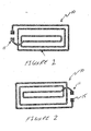
- Figure 1 illustrates a typical RFID antenna 10.
- the antenna may be in virtually any desired shape.
- Contact pads 11 for attachment of the antenna to the die are located at each end of the antenna.
- Figure 2 illustrates antenna 10 having pre-applied adhesive 15 on contact pads 11.
- the pre-applied adhesive would, after application, be in the form of a film that would be capable of reverting to a softened state at a sufficiently high temperature and then bonding the die to the antenna if it is a thermally activated film.
- the film is pressure sensitive in nature, then the die can be attached to the antenna with pressure.
- an antenna having at least two contact pads is first provided.
- Antennas are typically prepared with wet processes, such as screen printing of conductive inks or solution etching of copper/aluminum foil.
- an adhesive is deposited on one or more of the contact pads.
- the adhesive may be applied to the antenna via conventional printing or dispensing techniques at either room temperature or, if necessary, high temperature.
- the adhesive may be applied as a film or in a form capable of forming a film on the contact pad and may be either conductive or non-conductive.
- the adhesive may then be B-staged onto the antenna contact pads or B-staged onto release liner prior to placement on the antenna contact pads.
- a solvent-based adhesive for example, is B-staged onto the antenna contact pad by the evaporation of the solvent.
- a hot melt adhesive is B-staged onto the antenna contact pad after cooling back to room temperature
- a pressure sensitive adhesive may be utilized.
- an adhesive with multiple cure mechanisms is B-staged by partially curing the adhesive through the primary cure mechanism.
- the primary cure mechanism may consist of a thermal cure with a low temperature hardener or a UV cure hardener. Regardless of the method used to B-stage the adhesive, this process results in the formation of an adhesive film, at room temperature, on the antenna contact pads.
- the antenna with the pre-applied adhesives is first brought into contact with the die or die strap. If a thermally activated film is used, the assembly is then heated to a temperature sufficiently high to facilitate adhesive wetting. Wetting is crucial for proper bonding. During the heating process, the pre-applied adhesive softens and then adheres the die or die strap to the antenna. If the film is pressure sensitive in nature, then heat is not required. The die is then attached to the antenna with pressure.
- the pre-applied adhesive provides the numerous benefits to the manufacture and process of RFID antennas. For example, the pre-applied adhesive allows for fast, simplified processing for tag assemblers. Further, the pre-applied adhesive eliminates the capital expense required for tag assembly companies to apply the adhesive necessary for the attachment of the die or die strap.
Landscapes
- Engineering & Computer Science (AREA)
- Microelectronics & Electronic Packaging (AREA)
- Computer Hardware Design (AREA)
- Physics & Mathematics (AREA)
- General Physics & Mathematics (AREA)
- Theoretical Computer Science (AREA)
- Details Of Aerials (AREA)
- Support Of Aerials (AREA)
Abstract
Description
- The present invention relates to an antenna with a pre-applied adhesive for use with a radio frequency identification system and a method for assembling a radio frequency identification system using an antenna with a pre-applied adhesive.
- Radio frequency identification systems ("RFID") are frequently utilized in many applications, such as electronic surveillance and inventory tracking. RFID systems typically consist of a data carrier, such as a tag or transponder, and a reader. The tags or transponders are used in various formats, such as disks, smart cards, plastic housings, or in paper-thin tags. The tags consist of a silicon die attached to the contact pads on the antenna. Anisotropic or isotropic conductive pastes, anisotropic conductive films and non-conductive pastes are utilized to attach the antenna to the die. To attach the silicone chip to the antenna, manufacturers frequently utilize semiconductor flip chip technology processes. Via the flip chip process, the radio frequency identification dies are picked and placed onto the antenna after an anisotropic conductive adhesive is applied to the pads. The adhesive is then cured at a high temperature for a short time while pressure is applied on top of the die to ensure electrical connection. Due to a number of variables, the flip chip process often has the drawback of a relatively slow processing speed
- In all of the existing processes for assembling RFID systems adhesives are applied in a liquid or film form immediately before the die is attached to the antenna after which the unit is cured via heat or energy radiation. Numerous difficulties are presented by the use of such adhesives. For example, the die are extremely small and usually only a few millimeters square in size. Thus, the distances between the attachment bumps on the die are too small to utilize isotropic conductive paste.
- Die straps which allow for high speed reel-to-reel processing of the interconnection between the die and the antenna may be utilized. Such high speed processing is critical to manufacturers in order to produce the extremely large number of tags utilized in various industries. The use of high speed processing poses a number of difficulties for manufacturers. For example, high speed processing limits the type of adhesive application techniques and the type of adhesive that may be utilized. A low viscosity adhesive is required for high speed adhesive deposition. However, a low viscosity adhesive tends to have low green strength. Low green strength may cause the die to short after placement on the antenna pads because of the vibration experienced during high web processing speeds. Further, as adhesive has a limited work life, there will be a limited time during which the adhesive may be applied without a variation in its viscosity. To avoid the variation, manufacturers are required to interrupt the assembly process to insert fresh conductive adhesive, resulting in an inefficient process having downtime. It would be advantageous to provide an RFID antenna that could be readily utilized in a high speed assembly process along with a method for assembling RFID systems at a high speed.
-
- Figure 1 is a top view of an RFID antenna.
- Figure 2 is a top view of an RFID antenna having adhesive pre-applied to its contact pads.
- The present invention discloses an RFID antenna having adhesive pre-applied to one or more of its contact pads to allow for high speed attachment of the antenna to the RFID die or die strap. Also disclosed is a method for attaching an RFID antenna having pre-applied adhesive to a die or die strap.
- During assembly of RFID systems, RFID antennas are attached to the die or die strap to form an RFID data carrier. In order to facilitate high speed processing of the systems, it is desirable to utilize pre-applied adhesives on the contact pads of the RFID antennas. While the present application discusses antennas having two contact pads, it is possible for the antenna to have more than two contact pads and such embodiments are also within the scope of this invention. Antennas with pre-applied adhesive will simplify the die attach assembly process and reduce the production cost to the RFID manufacturers. Currently, RFID system manufacturers apply the adhesives to the antenna, resulting in additional steps in the assembly process. Through the use of the antennas with pre-applied adhesive of the present invention, the RFID system production time will not be limited by the ability to apply adhesives at a sufficiently high speed. The RFID system manufacturers will not be exposed to liquid adhesives, resulting in reduced waste, cleanup time and maintenance time, along with a reduced risk of exposure of its personnel to hazardous chemicals. Further, the softened or melted pre-applied adhesives of the present invention will possess a higher green strength than the liquid adhesives currently utilized resulting in a reduction of mis-alignments between the die and antenna contact pads before curing of the adhesive. Overall, the use of the pre-applied adhesives on the antenna will result in less processing variability and better interconnect quality.
- Various types of adhesives, including liquid paste, with or without solvent, and films may be utilized as a pre-applied adhesive on the antenna. The adhesives may be based on either thermoset or thermoplastic chemistry and should preferably have quick or snap bond capability. Depending upon the desired use, the adhesive may be either electrically conductive or electrically non-conductive. In the case that the adhesive is electrically conductive, it may be either anisotropic or isotropic.
- Figure 1 illustrates a
typical RFID antenna 10. Despite the illustrated configuration ofantenna 10, the antenna may be in virtually any desired shape. Contact pads 11 for attachment of the antenna to the die are located at each end of the antenna. Figure 2 illustratesantenna 10 having pre-applied adhesive 15 on contact pads 11. The pre-applied adhesive would, after application, be in the form of a film that would be capable of reverting to a softened state at a sufficiently high temperature and then bonding the die to the antenna if it is a thermally activated film. One the other hand, if the film is pressure sensitive in nature, then the die can be attached to the antenna with pressure. - In the method of pre-applying the adhesive, an antenna having at least two contact pads is first provided. Antennas are typically prepared with wet processes, such as screen printing of conductive inks or solution etching of copper/aluminum foil. Next, an adhesive is deposited on one or more of the contact pads. The adhesive may be applied to the antenna via conventional printing or dispensing techniques at either room temperature or, if necessary, high temperature. The adhesive may be applied as a film or in a form capable of forming a film on the contact pad and may be either conductive or non-conductive. The adhesive may then be B-staged onto the antenna contact pads or B-staged onto release liner prior to placement on the antenna contact pads. Many types of adhesives, including solvent-based adhesives, hot melt adhesives and also adhesives with dual cure mechanisms are suitable as B-stage adhesives. A solvent-based adhesive, for example, is B-staged onto the antenna contact pad by the evaporation of the solvent. A hot melt adhesive, on the other hand, is B-staged onto the antenna contact pad after cooling back to room temperature In a further embodiment, a pressure sensitive adhesive may be utilized. Finally, an adhesive with multiple cure mechanisms is B-staged by partially curing the adhesive through the primary cure mechanism. The primary cure mechanism may consist of a thermal cure with a low temperature hardener or a UV cure hardener. Regardless of the method used to B-stage the adhesive, this process results in the formation of an adhesive film, at room temperature, on the antenna contact pads. For bonding of the antenna to the die, the antenna with the pre-applied adhesives is first brought into contact with the die or die strap. If a thermally activated film is used, the assembly is then heated to a temperature sufficiently high to facilitate adhesive wetting. Wetting is crucial for proper bonding. During the heating process, the pre-applied adhesive softens and then adheres the die or die strap to the antenna. If the film is pressure sensitive in nature, then heat is not required. The die is then attached to the antenna with pressure.
- The pre-applied adhesive provides the numerous benefits to the manufacture and process of RFID antennas. For example, the pre-applied adhesive allows for fast, simplified processing for tag assemblers. Further, the pre-applied adhesive eliminates the capital expense required for tag assembly companies to apply the adhesive necessary for the attachment of the die or die strap.
- Many modifications and variations of this invention can be made without departing from its spirit and scope, as will be apparent to those skilled in the art. The specific embodiments described herein are offered by way of example only, and the invention is to be limited only by the terms of the appended claims, along with the full scope of equivalents to which such claims are entitled.
Claims (11)
- A method for preparing a radio frequency identification data carrier antenna comprising the steps of:providing a radio frequency identification antenna having more than one contact pad; andapplying an adhesive to at least one of the more than one contact pads;wherein the adhesive forms a film on at least one of the more than one contact pads.
- The method of claim 1, further comprising the step of B-staging the adhesive on at least one of the more than one contact pads.
- The method of claim 1 further comprising the step of B-staging the adhesive on a release liner.
- The method of claim 1, further comprising the step of heating the data carrier to a temperature sufficiently high to cause wetting of the pre-applied adhesive.
- The method of claim 1, wherein the adhesive is a pressure sensitive adhesive.
- The method of claim 4, further comprising the step of attaching the more than one contact pads of the antenna to a die or die strap.
- The method of claim 1, wherein the adhesive consists of a thermoplastic adhesive or a thermoset adhesive.
- The method of claim 1, wherein the adhesive consists of an electrically conductive adhesive.
- The method of claim 8, wherein the adhesive is an anisotropic adhesive or an isotropic adhesive.
- An antenna for use in an radio frequency identification system having more than one contact pads, wherein at least one of the more than one contact pads have a pre-applied adhesive applied thereon.
- The antenna of claim 10, wherein the pre-applied adhesive is in the form of a film.
Applications Claiming Priority (1)
| Application Number | Priority Date | Filing Date | Title |
|---|---|---|---|
| US11/255,117 US7456748B2 (en) | 2005-10-20 | 2005-10-20 | RFID antenna with pre-applied adhesives |
Publications (1)
| Publication Number | Publication Date |
|---|---|
| EP1780663A1 true EP1780663A1 (en) | 2007-05-02 |
Family
ID=37622208
Family Applications (1)
| Application Number | Title | Priority Date | Filing Date |
|---|---|---|---|
| EP06021945A Withdrawn EP1780663A1 (en) | 2005-10-20 | 2006-10-19 | RFID antenna with pre-applied adhesives |
Country Status (6)
| Country | Link |
|---|---|
| US (1) | US7456748B2 (en) |
| EP (1) | EP1780663A1 (en) |
| JP (1) | JP2007115249A (en) |
| KR (1) | KR20070043635A (en) |
| CN (1) | CN1953270A (en) |
| TW (1) | TW200733470A (en) |
Families Citing this family (8)
| Publication number | Priority date | Publication date | Assignee | Title |
|---|---|---|---|---|
| US7701352B2 (en) * | 2006-11-22 | 2010-04-20 | Avery Dennison Corporation | RFID label with release liner window, and method of making |
| US7683836B2 (en) * | 2007-06-13 | 2010-03-23 | World Properties, Inc. | Antenna with thermally transferred element |
| US9286511B2 (en) | 2013-01-22 | 2016-03-15 | Amerasia International Technology, Inc. | Event registration and management system and method employing geo-tagging and biometrics |
| US9814278B2 (en) | 2014-10-17 | 2017-11-14 | Avante International Technology, Inc. | Protective headgear including a personnel electronic monitor device |
| US10019881B2 (en) | 2015-11-04 | 2018-07-10 | Streamlight, Inc. | Personnel tracking and monitoring system and method employing protective gear including a personnel electronic monitor device |
| US10713697B2 (en) | 2016-03-24 | 2020-07-14 | Avante International Technology, Inc. | Farm product exchange system and method suitable for multiple small producers |
| US10546226B2 (en) * | 2016-07-07 | 2020-01-28 | Avery Dennison Retail Information Services Llc | Feedback control of mounted chip production |
| WO2020219525A1 (en) * | 2019-04-22 | 2020-10-29 | Avery Dennison Retail Information Services, Llc | Self-adhesive straps for rfid devices |
Citations (8)
| Publication number | Priority date | Publication date | Assignee | Title |
|---|---|---|---|---|
| DE19732645A1 (en) * | 1997-07-29 | 1998-09-10 | Siemens Ag | Combination chip card manufacturing method |
| FR2785071A1 (en) * | 1998-10-26 | 2000-04-28 | Gemplus Card Int | METHOD FOR MANUFACTURING A CHIP CARD AND AN ELECTRONIC MODULE TO BE INSERTED IN SUCH A CARD |
| US6665193B1 (en) * | 2002-07-09 | 2003-12-16 | Amerasia International Technology, Inc. | Electronic circuit construction, as for a wireless RF tag |
| US6677186B1 (en) * | 1999-03-12 | 2004-01-13 | Gemplus | Method for making an electronic device such as a contactless card |
| EP1432021A2 (en) * | 2002-12-17 | 2004-06-23 | Omron Corporation | Manufacturing method for electronic component module and electromagnetically readable data carrier |
| WO2004110119A1 (en) * | 2003-06-04 | 2004-12-16 | Upm Rafsec Oy | A method for forming a joint |
| FR2861201A1 (en) * | 2003-10-17 | 2005-04-22 | Oberthur Card Syst Sa | METHOD FOR MANUFACTURING A CARD WITH A DOUBLE INTERFACE, AND MICROCIRCUIT CARD THUS OBTAINED |
| US20050110129A1 (en) * | 2002-03-18 | 2005-05-26 | Toray Engineering Company, Ltd | Noncontact ID card and method of manufacturing the same |
Family Cites Families (8)
| Publication number | Priority date | Publication date | Assignee | Title |
|---|---|---|---|---|
| FI20001344L (en) * | 2000-06-06 | 2001-12-07 | Rafsec Oy | Method and apparatus for manufacturing a smart label feed web |
| US6951596B2 (en) * | 2002-01-18 | 2005-10-04 | Avery Dennison Corporation | RFID label technique |
| JP2004086852A (en) * | 2002-03-18 | 2004-03-18 | Toray Eng Co Ltd | Non-contact id card or the like, and its manufacturing method |
| AU2003276729A1 (en) * | 2002-06-17 | 2003-12-31 | Henkel Corporation | Interlayer dielectric and pre-applied die attach adhesive materials |
| US7224280B2 (en) * | 2002-12-31 | 2007-05-29 | Avery Dennison Corporation | RFID device and method of forming |
| US6940408B2 (en) * | 2002-12-31 | 2005-09-06 | Avery Dennison Corporation | RFID device and method of forming |
| JP4245370B2 (en) * | 2003-02-21 | 2009-03-25 | 大日本印刷株式会社 | Manufacturing method of semiconductor device |
| JP3803097B2 (en) * | 2003-10-07 | 2006-08-02 | 株式会社日立製作所 | Method for manufacturing wireless communication medium |
-
2005
- 2005-10-20 US US11/255,117 patent/US7456748B2/en not_active Expired - Fee Related
-
2006
- 2006-10-16 JP JP2006281364A patent/JP2007115249A/en active Pending
- 2006-10-17 CN CNA2006101357172A patent/CN1953270A/en active Pending
- 2006-10-19 KR KR1020060101804A patent/KR20070043635A/en not_active Withdrawn
- 2006-10-19 EP EP06021945A patent/EP1780663A1/en not_active Withdrawn
- 2006-10-19 TW TW095138494A patent/TW200733470A/en unknown
Patent Citations (8)
| Publication number | Priority date | Publication date | Assignee | Title |
|---|---|---|---|---|
| DE19732645A1 (en) * | 1997-07-29 | 1998-09-10 | Siemens Ag | Combination chip card manufacturing method |
| FR2785071A1 (en) * | 1998-10-26 | 2000-04-28 | Gemplus Card Int | METHOD FOR MANUFACTURING A CHIP CARD AND AN ELECTRONIC MODULE TO BE INSERTED IN SUCH A CARD |
| US6677186B1 (en) * | 1999-03-12 | 2004-01-13 | Gemplus | Method for making an electronic device such as a contactless card |
| US20050110129A1 (en) * | 2002-03-18 | 2005-05-26 | Toray Engineering Company, Ltd | Noncontact ID card and method of manufacturing the same |
| US6665193B1 (en) * | 2002-07-09 | 2003-12-16 | Amerasia International Technology, Inc. | Electronic circuit construction, as for a wireless RF tag |
| EP1432021A2 (en) * | 2002-12-17 | 2004-06-23 | Omron Corporation | Manufacturing method for electronic component module and electromagnetically readable data carrier |
| WO2004110119A1 (en) * | 2003-06-04 | 2004-12-16 | Upm Rafsec Oy | A method for forming a joint |
| FR2861201A1 (en) * | 2003-10-17 | 2005-04-22 | Oberthur Card Syst Sa | METHOD FOR MANUFACTURING A CARD WITH A DOUBLE INTERFACE, AND MICROCIRCUIT CARD THUS OBTAINED |
Also Published As
| Publication number | Publication date |
|---|---|
| JP2007115249A (en) | 2007-05-10 |
| US7456748B2 (en) | 2008-11-25 |
| TW200733470A (en) | 2007-09-01 |
| US20070089286A1 (en) | 2007-04-26 |
| KR20070043635A (en) | 2007-04-25 |
| CN1953270A (en) | 2007-04-25 |
Similar Documents
| Publication | Publication Date | Title |
|---|---|---|
| EP1399881B1 (en) | A smart label and a smart label web | |
| US20040026033A1 (en) | High speed flip chip assembly process | |
| EP1769430B1 (en) | Rfid device and method of forming | |
| US7884726B2 (en) | Transfer tape strap process | |
| EP2323079A2 (en) | Electrical device manufacturing techniques | |
| US7102520B2 (en) | RFID device and method of forming | |
| JP3248518U (en) | Apparatus for forming labels with integrated conductive patterns - Patent Application 20070123633 | |
| WO2002082368A1 (en) | A smart card web and a method for its manufacture | |
| US20080129455A1 (en) | Method for forming rfid tags | |
| EP1930844B1 (en) | Noncontact information storage medium and method for manufacturing same | |
| US7456748B2 (en) | RFID antenna with pre-applied adhesives | |
| CN111448572B (en) | Method and device for producing radio frequency identification transponder | |
| US7884719B2 (en) | Radio frequency identification (RFID) tag lamination process | |
| EP3846082A1 (en) | Heat transfer rfid tag for fabric and method of manufacturing the same | |
| US7674649B2 (en) | Radio frequency identification (RFID) tag lamination process using liner | |
| US7456506B2 (en) | Radio frequency identification (RFID) tag lamination process using liner | |
| EP1703448A2 (en) | RFID tag, module component, and RFID tag fabrication method | |
| EP3704635B1 (en) | Method for manufacturing an rfid tag and an rfid tag comprising an ic and an antenna | |
| KR20100043945A (en) | Manufacturing method and apparatus of radio frequency identification tag | |
| CN210924630U (en) | Thermal transfer printing RFID label structure of fabric | |
| KR20120033732A (en) | Method of manufacturing foldable carton having electric tag | |
| JP2002221902A (en) | Luggage paper tags and their manufacturing method | |
| EP1947918B1 (en) | Electronic device and method of manufacturing same | |
| KR20090084499A (en) | Method for manufacturing radio frequency identification tag and radio frequency identification tag manufactured by the same | |
| Gillissen et al. | Low temperature snap cure thermoset adhesives with good worklife |
Legal Events
| Date | Code | Title | Description |
|---|---|---|---|
| PUAI | Public reference made under article 153(3) epc to a published international application that has entered the european phase |
Free format text: ORIGINAL CODE: 0009012 |
|
| AK | Designated contracting states |
Kind code of ref document: A1 Designated state(s): AT BE BG CH CY CZ DE DK EE ES FI FR GB GR HU IE IS IT LI LT LU LV MC NL PL PT RO SE SI SK TR |
|
| AX | Request for extension of the european patent |
Extension state: AL BA HR MK YU |
|
| 17P | Request for examination filed |
Effective date: 20071022 |
|
| 17Q | First examination report despatched |
Effective date: 20071120 |
|
| AKX | Designation fees paid |
Designated state(s): AT BE BG CH CY CZ DE DK EE ES FI FR GB GR HU IE IS IT LI LT LU LV MC NL PL PT RO SE SI SK TR |
|
| RAP1 | Party data changed (applicant data changed or rights of an application transferred) |
Owner name: HENKEL AG & CO. KGAA |
|
| STAA | Information on the status of an ep patent application or granted ep patent |
Free format text: STATUS: THE APPLICATION IS DEEMED TO BE WITHDRAWN |
|
| 18D | Application deemed to be withdrawn |
Effective date: 20090709 |