EP1776000A2 - 8-Pin PFC and ballast control IC - Google Patents
8-Pin PFC and ballast control IC Download PDFInfo
- Publication number
- EP1776000A2 EP1776000A2 EP06021446A EP06021446A EP1776000A2 EP 1776000 A2 EP1776000 A2 EP 1776000A2 EP 06021446 A EP06021446 A EP 06021446A EP 06021446 A EP06021446 A EP 06021446A EP 1776000 A2 EP1776000 A2 EP 1776000A2
- Authority
- EP
- European Patent Office
- Prior art keywords
- pin
- circuit
- voltage
- during
- power circuit
- Prior art date
- Legal status (The legal status is an assumption and is not a legal conclusion. Google has not performed a legal analysis and makes no representation as to the accuracy of the status listed.)
- Withdrawn
Links
Images

Classifications
-
- H—ELECTRICITY
- H05—ELECTRIC TECHNIQUES NOT OTHERWISE PROVIDED FOR
- H05B—ELECTRIC HEATING; ELECTRIC LIGHT SOURCES NOT OTHERWISE PROVIDED FOR; CIRCUIT ARRANGEMENTS FOR ELECTRIC LIGHT SOURCES, IN GENERAL
- H05B41/00—Circuit arrangements or apparatus for igniting or operating discharge lamps
- H05B41/14—Circuit arrangements
- H05B41/26—Circuit arrangements in which the lamp is fed by power derived from dc by means of a converter, e.g. by high-voltage dc
- H05B41/28—Circuit arrangements in which the lamp is fed by power derived from dc by means of a converter, e.g. by high-voltage dc using static converters
- H05B41/295—Circuit arrangements in which the lamp is fed by power derived from dc by means of a converter, e.g. by high-voltage dc using static converters with semiconductor devices and specially adapted for lamps with preheating electrodes, e.g. for fluorescent lamps
- H05B41/298—Arrangements for protecting lamps or circuits against abnormal operating conditions
-
- H—ELECTRICITY
- H05—ELECTRIC TECHNIQUES NOT OTHERWISE PROVIDED FOR
- H05B—ELECTRIC HEATING; ELECTRIC LIGHT SOURCES NOT OTHERWISE PROVIDED FOR; CIRCUIT ARRANGEMENTS FOR ELECTRIC LIGHT SOURCES, IN GENERAL
- H05B41/00—Circuit arrangements or apparatus for igniting or operating discharge lamps
-
- H—ELECTRICITY
- H02—GENERATION; CONVERSION OR DISTRIBUTION OF ELECTRIC POWER
- H02M—APPARATUS FOR CONVERSION BETWEEN AC AND AC, BETWEEN AC AND DC, OR BETWEEN DC AND DC, AND FOR USE WITH MAINS OR SIMILAR POWER SUPPLY SYSTEMS; CONVERSION OF DC OR AC INPUT POWER INTO SURGE OUTPUT POWER; CONTROL OR REGULATION THEREOF
- H02M1/00—Details of apparatus for conversion
- H02M1/42—Circuits or arrangements for compensating for or adjusting power factor in converters or inverters
- H02M1/4208—Arrangements for improving power factor of AC input
- H02M1/4225—Arrangements for improving power factor of AC input using a non-isolated boost converter
-
- H—ELECTRICITY
- H05—ELECTRIC TECHNIQUES NOT OTHERWISE PROVIDED FOR
- H05B—ELECTRIC HEATING; ELECTRIC LIGHT SOURCES NOT OTHERWISE PROVIDED FOR; CIRCUIT ARRANGEMENTS FOR ELECTRIC LIGHT SOURCES, IN GENERAL
- H05B41/00—Circuit arrangements or apparatus for igniting or operating discharge lamps
- H05B41/14—Circuit arrangements
- H05B41/24—Circuit arrangements in which the lamp is fed by high frequency ac, or with separate oscillator frequency
-
- H—ELECTRICITY
- H05—ELECTRIC TECHNIQUES NOT OTHERWISE PROVIDED FOR
- H05B—ELECTRIC HEATING; ELECTRIC LIGHT SOURCES NOT OTHERWISE PROVIDED FOR; CIRCUIT ARRANGEMENTS FOR ELECTRIC LIGHT SOURCES, IN GENERAL
- H05B41/00—Circuit arrangements or apparatus for igniting or operating discharge lamps
- H05B41/14—Circuit arrangements
- H05B41/26—Circuit arrangements in which the lamp is fed by power derived from dc by means of a converter, e.g. by high-voltage dc
- H05B41/28—Circuit arrangements in which the lamp is fed by power derived from dc by means of a converter, e.g. by high-voltage dc using static converters
- H05B41/295—Circuit arrangements in which the lamp is fed by power derived from dc by means of a converter, e.g. by high-voltage dc using static converters with semiconductor devices and specially adapted for lamps with preheating electrodes, e.g. for fluorescent lamps
- H05B41/298—Arrangements for protecting lamps or circuits against abnormal operating conditions
- H05B41/2981—Arrangements for protecting lamps or circuits against abnormal operating conditions for protecting the circuit against abnormal operating conditions
-
- Y—GENERAL TAGGING OF NEW TECHNOLOGICAL DEVELOPMENTS; GENERAL TAGGING OF CROSS-SECTIONAL TECHNOLOGIES SPANNING OVER SEVERAL SECTIONS OF THE IPC; TECHNICAL SUBJECTS COVERED BY FORMER USPC CROSS-REFERENCE ART COLLECTIONS [XRACs] AND DIGESTS
- Y02—TECHNOLOGIES OR APPLICATIONS FOR MITIGATION OR ADAPTATION AGAINST CLIMATE CHANGE
- Y02B—CLIMATE CHANGE MITIGATION TECHNOLOGIES RELATED TO BUILDINGS, e.g. HOUSING, HOUSE APPLIANCES OR RELATED END-USER APPLICATIONS
- Y02B70/00—Technologies for an efficient end-user side electric power management and consumption
- Y02B70/10—Technologies improving the efficiency by using switched-mode power supplies [SMPS], i.e. efficient power electronics conversion e.g. power factor correction or reduction of losses in power supplies or efficient standby modes
Definitions
- the present invention relates to a fluorescent ballast control integrated circuit (IC) with power factor correction (PFC), and more particularly to a ballast control IC with a low pin count and improved programmability.
- the invention relates further to control methods performed by the IC.
- Ballast control IC's of background interest are described in U.S. Patents 5,545,955 ; 6,211,623 ; 6,259,614 ; 6,617,805 ; and U.S. application serial no. 10/875,474 (allowed), all incorporated by reference.
- the present invention provides a PFC, ballast control and half-bridge driver in one IC.
- Other features include:
- the disclosed IC and method includes high-voltage sensing circuits to perform various PFC and ballast system functions.
- a single high-voltage pin senses PFC zero crossing and over-current.
- a second high-voltage pin senses the DC bus voltage and the half-bridge current.
- Programmable ballast parameters include pre-heat time, preheat frequency and run frequency. Protection features include ignition regulation, lamp non-strike protection, open filaments, end-of-life, lamp removal and automatic restrike. Combining these high-voltage control techniques together with programmable ballast parameters and complete fault protection in a single 8-pin IC results in a massive reduction in component count, an increase in manufacturability, and greater reliability, while maintaining high ballast system performance.
- the benefits of the disclosed IC and method include:
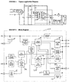
- Fig. 1 is a schematic diagram showing a typical application of the IC.
- Fig. 2 is a block diagram of the IC.
- Fig. 3 is a state diagram showing sequences of operations in the IC.
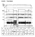
- Fig. 4 is a timing diagram showing signals in the IC.
- the ballast control circuit 100 contains functions to properly control all types of fluorescent lamps. These functions include preheat frequency, preheat time, run frequency, ignition voltage regulation, lamp non-strike protection, lamp removal or open circuit protection, lamp replacement automatic restart, and lamp end-of-life protection.
- the modes or 'states' of the control circuit include:
- UVLO Under-voltage Lock-out
- the enabled circuits include the UVLO circuit 10 itself, the restart logic circuit 12 and the preheat frequency read/set circuit 22.
- the complete PFC circuit is disabled and the PFC gate driver 14 output is off (logic 'low') to ensure that the external PFC MOSFET MPFC is in a defined state and does not turn on unexpectedly.
- the ballast oscillator 16 is disabled and the high-side gate driver 18 output (HO pin) is off (logic 'low').
- the low-side gate driver 20 output (LO pin) is used as an input pin during UVLO Mode for the restart logic circuit 12 and the preheat frequency read/set circuit 22.
- the use of the LO pin as an input pin during UVLO mode is a useful feature of this circuit.
- Traditional half-bridge driver circuits disable both LO and HO pins (both off, logic 'low) during UVLO mode to prevent the external half-bridge MOSFETs from turning on unexpectedly. If the upper MOSFET MHS of the totem-pole configuration is off then it does not matter if the lower MOSFET MLS is on or offbecause no voltage will be generated at the half-bridge mid-point. The LO pin is therefore available to use as an input during UVLO and Fault Modes.
- LO pin as an automatic restart input to detect when the lamp has been removed and reinserted, and, as an input to program the preheat frequency, eliminates the need for additional pins to realize these functions.
- LO pin as input during UVLO mode is one of the useful features of this circuit that allows for the entire PFC and ballast circuit to be realized in a simple 8-pin IC package.
- a current source is connected to the LO pin. This current flows through a resistor (RFPH) that is connected between the LO pin and COM. The resulting voltage at the LO pin is measured by the read/set circuit 22 and is used to set the preheat frequency of the ballast oscillator 16.
- the restart circuit 12 also measures the LO pin voltage during UVLO Mode to detect if a lamp is inserted in the lamp resonant output stage. If a lamp is not inserted, the resistor RFPH will pull-up to VCC and pull the LO pin above the restart threshold voltage (10V typical) and prevent the IC from exiting UVLO mode.
- resistor RFPH will be connected through the lower lamp filament to COM (see Figure 1, Typical Application Schematic Diagram) and will pull the voltage on the LO pin below the restart threshold voltage. If the LO pin voltage is below the restart threshold and the VCC supply voltage is above the UVLO+ turn-on threshold, then the IC will exit UVLO Mode and enter Read/Set Mode. During UVLO Mode, the circuit draws only a small amount of 'micro-power' current (200uA typical). This micro-power current, together with the resistor RVCC connected between VCC and the AC mains rectified input voltage and the WLO+ threshold, sets the AC mains turn-on voltage for the complete electronic ballast.
- UVLO Mode the circuit outputs a source current at the LO pin.
- An external resistor RFPH is connected between the LO pin and COM. This current flows through resistor RFPH resulting in a voltage level at the LO pin.
- VCC exceeds the UVLO+ threshold
- the circuit enters Read/Set Mode and the read/set circuit measures the voltage at the LO pin and sets the corresponding preheat frequency. This is accomplished using several comparators that measure the voltage at the LO pin during Read/Set Mode and compares it against several pre-determined voltage levels.
- the voltage range that the LO pin voltage falls into determines which comparator outputs will go 'high' or 'low', and these 'high' and 'low' logic signals are used to set the appropriate latch circuit to set the correct oscillator 16 frequency during preheat.
- the number of comparators determines the amount of programming resolution. 32 comparators, for example, will give a resolution of 32 levels of preheat frequency programmability. As soon as the preheat frequency has been set, the ballast control circuit 100 then exits Read/Set Mode and enters Preheat Mode.
- the circuit enters Preheat Mode when VCC exceeds the UVLO+ threshold voltage and the preheat frequency has been set.
- the PFC circuit ( ) becomes active and the PFC pin oscillates at the correct on and off time for high power factor and regulation of the DC bus voltage to a constant level.
- the ballast oscillator 16 becomes active and the LO gate driver output turns on first.
- the LO pin sources a gate drive current (300mA typical) to turn on the external low-side half-bridge MOSFET MLS.
- the voltage level at the LO pin becomes limited by the zener diode, DTPH, that is connected between the LO pin and COM.
- the preheat time read/set circuit measures the voltage at the LO pin during the first LO on-time pulse and sets the corresponding ballast preheat time. Similar to the preheat frequency read/set circuit 22, this is accomplished using several comparators and voltage levels and the number of comparators determines the amount of programming resolution.
- the minimum zener voltage of the zener diode DTPH connected to the LO pin should be higher than the VCC UVLO+ threshold in order to allow for the circuit to exit UVLO Mode.
- HO and LO begin oscillating normally at an initial soft-start frequency that is a fixed percentage higher than the preheat frequency.
- HO and LO oscillate on and off at a 50% duty-cycle and with a non-overlapping dead-time (1.5usec typical) between LO-to-HO and HO-to-LO switching transitions.
- the frequency quickly ramps down to the set preheat frequency and remains at the preheat frequency for the duration of the preheat time.
- the preheat time was set during the initial on-time pulse at the LO pin at the start of preheat with the zener diode, DTPH, connected between LO and COM. This caused a corresponding internal voltage level (VTPH) to be set that is compared against an internal ramping capacitor, CPH.
- the internal capacitor, CPH is ramped up with small pulses (100nsec typical) that occur once each cycle of the ballast oscillator 16. This causes the voltage on capacitor CPH to charge up in a 'stair-step' fashion. By controlling CPH in this stair-step manner, a very small capacitor can be used for CPH.
- the preheat time is therefore dependent on the preheat frequency and the external zener diode at the LO pin.
- the ballast control circuit exits Preheat Mode and enters Ignition Mode.
- the non-ZVS protection circuit 24 is also active and detects ifhard-switching occurs at the half-bridge mid-point. Should non-ZVS occur due to lamp removal, filament failure or open circuit, the circuit will enter Fault Mode after for example 50 events of non-ZVS have occurred.
- the non-ZVS circuit detects hard-switching using an additional high-voltage sensing MOSFET that is connected to the mid-point of the half-bridge. This MOSFET is turned on at the turn-off of HO (start of the dead-time) and the voltage at the VS pin is measured at the turn-on of LO (end of the dead-time). If the voltage is non-zero then this is determined to be a non-ZVS fault occurrence.
- the circuit enters Ignition Mode when the internal preheat timing capacitor, CPH, exceeds the set preheat time voltage level (VTPH) for the first time. CPH is then discharged quickly to COM and then begins charging up again in the same 'stair-step' fashion as during Preheat Mode.
- the ballast oscillator 16 frequency begins ramping the frequency down at a pre-determined rate from the preheat frequency to the final run frequency. This will cause the voltage across the fluorescent lamp L to increase as the frequency decreases towards the resonance frequency of the resonant lamp output stage. When the lamp voltage reaches the required lamp ignition voltage, the lamp will ignite. The frequency will continue to ramp down until it reaches the final running frequency.
- the lamp voltage and inductor tank current will continue to increase until the inductor saturates.
- the di/dt circuit 26 will detect the sharp increase in the slope of the inductor current and then increase the frequency by a pre-determined amount to decrease on-time of LO and HO.
- the decrease in the on-time of LO and HO will cause the corresponding external MOSFET MHS, MLS to turn-off earlier each cycle. This will decrease the peak current that the inductor charges up to so that it is just below the saturation level.
- the frequency will remain at this level to keep the inductor current just below saturation for the duration of the Ignition Mode time.
- Regulating the inductor current just below the saturation level results in an adaptive ignition regulation control circuit ( ).
- This circuit will regulate the maximum inductor current just below the saturation level regardless of temperature and/or the size or type of the inductor used, and eliminates the need for a precise current sensing resistor typically used with traditional ballast control methods. Regulating the current just below the saturation level will also cause the voltage across the lamp to be regulated to a constant level for the duration of the ignition time.
- This ignition regulation feature significantly increases the reliability of igniting the lamp. This is especially useful at low temperatures or when igniting old lamps and can therefore increase the lifetime of the lamp by allowing for a higher number of ignitions to occur before the lamp is replaced.
- the inductor current is sensed using a high-voltage sensing MOSFET that is connected to the mid-point of the half-bridge circuit (VS pin).
- a high-voltage sensing MOSFET that is connected to the mid-point of the half-bridge circuit (VS pin).
- the mid-point of the half-bridge is up at the DC bus voltage and the high-voltage sensing MOSFET is turned off and is blocking the high-voltage.
- the high-voltage MOSFET is turned on for measuring the voltage across the RDSon of the external lower half-bridge MOSFET MLS. Because this circuit detects di/dt, it is therefore independent of the RDSon value, which is different from MOSFET to MOSFET and changes with temperature.
- This run frequency is programmed with a zener diode, DFRUN, connected between VCC and COM.
- the resulting voltage level set on VCC with the zener diode, DFRUN sets the ramping threshold for a timing capacitor, CT.
- This timing capacitor is charged up linearly to VCC with a current source each switching cycle ofLO and HO.
- CT When CT reaches VCC, CT is discharged to COM instantly and the ramp charges again.
- the result is a 'saw-tooth' voltage waveform on CT, and each on-time ramp is toggled alternately between LO and HO gate driver outputs (see Figure 4, ballast oscillator timing diagram).
- the ignition regulation circuit is disabled and the circuit will enter Fault Mode if several events (50 events typical) of a di/dt greater than a maximum di/dt occur.
- the di/dt circuit will have regulated the inductor current just below saturation by holding the frequency at a constant level for the duration of Ignition Mode. Since the ignition regulation circuit becomes disabled in Run Mode, the frequency will start to decrease again towards the final run frequency. This will cause the inductor to saturate again and will be detected by the di/dt circuit 26. After several events (50 typical) of saturation are detected by the di/dt circuit 26, the ballast circuit will enter Fault Mode and shutdown the circuit safely before the high-current and high-voltage can damage circuit components or harm someone performing maintenance on the lamp.
- the DC bus under-voltage protection circuit is enabled. If the DC bus drops below an unsafe level, the circuit will detect this and discharge VCC below UVLO- to turn the ballast circuit off safely.
- the end-of-life (EOL) negative-going latched threshold (VCCEOL-) is also enabled at the VCC pin. Should end-of-life occur on the lamp, an asymmetrical shift in the lamp voltage can occur. This shift will be detected by an external circuit including QEOL and will pull VCC below VCCEOL- (10V typical). When VCC decreases below VCCEOL- during Run Mode, the circuit will latch off safely.
- the ballast circuit will enter Fault Mode and latch off safely and only draw micro-power current at VCC.
- the external supply resistor, RVCC will pull VCC up to the external zener diode voltage (DFRUN) and the circuit will remain in Fault Mode. If the voltage at the LO pin pulls up above the restart threshold (VRESTART+) due to a lamp removal, or, VCC is decreased below the lower UVLO- threshold (6V typical), then the latch will be reset and the complete circuit will enter UVLO Mode.
- non-ZVS protection 24 is also enabled. Should a non-ZVS condition occur during Run Mode due to a lamp removal fault or an open filament fault, then, similar to Preheat Mode, the non-ZVS protection circuit will detect the resulting hard-switching at the half-bridge mid-point (VS pin). After several events (50 typical) ofhard-switching, the ballast circuit will enter Fault Mode and latch the ballast circuit off safely.
- the ballast circuit will enter Fault Mode from Preheat Mode if several events of non-ZVS occur.
- the ballast circuit will enter Fault Mode from Run Mode if several events of non-ZVS or di/dt occur, or, VCC is less than VCCEOL-.
- the ballast 16 and PFC 26 oscillators are latched off and gate driver outputs HO and PFC are both turned 'off' (logic 'low').
- the circuit remains in this latched state while consuming only micro-power current (200uA typical) at VCC.
- the LO gate driver output goes open circuit and becomes an input for detecting if the lamp is exchanged. If the LO pin is pulled above VRESTART+ (lamp removal), or, VCC is decreased below UVLO- (AC mains voltage is turned off or interrupted), the fault latch will be reset and the ballast circuit will exit Fault Mode and enter UVLO Mode.
Abstract
Description
- This application is based upon and claims priority of
U.S. Provisional Serial No. 60/661,809 filed March 15, 2005 U.S. Provisional Serial No. 60/725,706 filed October 12, 2005 - The present invention relates to a fluorescent ballast control integrated circuit (IC) with power factor correction (PFC), and more particularly to a ballast control IC with a low pin count and improved programmability. The invention relates further to control methods performed by the IC.
- Ballast control IC's of background interest are described in
U.S. Patents 5,545,955 ;6,211,623 ;6,259,614 ;6,617,805 ; andU.S. application serial no. 10/875,474 (allowed), all incorporated by reference. - The present invention provides a PFC, ballast control and half-bridge driver in one IC. Other features include:
- Critical-conduction mode boost-type PFC
- Internal VBUS sensing and regulation
- Internal PFC over-current protection
- Internal PFC zero-crossing detection
- Internal PFC loop compensation
- Adaptive saturation ignition regulation
- Internal non-ZVS protection
- Programmable preheat time
- Programmable preheat frequency
- Programmable run frequency
- Latched negative-going threshold on VCC
- Fixed dead-time (1.5ustyp.)
- DC bus under-voltage reset
- Lamp insert auto-restart
- Up/down fault counter
- Internal bootstrap MOSFET
- Internal 15.6V zener clamp diode on Vcc
- Micropower startup (200µA)
- Latch immunity and ESD protection
- The disclosed IC and method includes high-voltage sensing circuits to perform various PFC and ballast system functions. A single high-voltage pin senses PFC zero crossing and over-current. A second high-voltage pin senses the DC bus voltage and the half-bridge current. Programmable ballast parameters include pre-heat time, preheat frequency and run frequency. Protection features include ignition regulation, lamp non-strike protection, open filaments, end-of-life, lamp removal and automatic restrike. Combining these high-voltage control techniques together with programmable ballast parameters and complete fault protection in a single 8-pin IC results in a massive reduction in component count, an increase in manufacturability, and greater reliability, while maintaining high ballast system performance.
- The benefits of the disclosed IC and method include:
- No PFC secondary winding required
- No PFC current-sensing resistor required
- No PFC compensation capacitor required
- No Half-bridge current-sensing resistor required
- No VBUS voltage sensing resistor network required
- No external bootstrap diode required
- Small 8-pin package
- Massive reduction in component count
- Increased manufacturability and reliability
- Fast design time
- Other features and advantages of the present invention will become apparent from the following description of embodiments of the invention which refers to the accompanying drawings.
- Fig. 1 is a schematic diagram showing a typical application of the IC.
- Fig. 2 is a block diagram of the IC.
- Fig. 3 is a state diagram showing sequences of operations in the IC.
- Fig. 4 is a timing diagram showing signals in the IC.
- Functional Description: Ballast Control Circuit
- The
ballast control circuit 100 contains functions to properly control all types of fluorescent lamps. These functions include preheat frequency, preheat time, run frequency, ignition voltage regulation, lamp non-strike protection, lamp removal or open circuit protection, lamp replacement automatic restart, and lamp end-of-life protection. The modes or 'states' of the control circuit include: - 1) UVLO Mode
- 2) Read/Set Mode
- 3) Preheat Mode
- 4) Ignition Mode
- 5) Run Mode
- 6) Fault Mode
- For a detailed flowchart between these states refer to the State Diagram in Figure 3.
- UVLO Mode (1)
- Under-voltage Lock-out (UVLO) Mode is the state the circuit (see Fig. 2) is in when the supply voltage at VCC is below the correct turn-on threshold voltage. During UVLO Mode, both the PFC and ballast circuits are disabled with only a minimum number of required functions enabled. The enabled circuits include the UVLO circuit 10 itself, the
restart logic circuit 12 and the preheat frequency read/set circuit 22. The complete PFC circuit is disabled and thePFC gate driver 14 output is off (logic 'low') to ensure that the external PFC MOSFET MPFC is in a defined state and does not turn on unexpectedly. Theballast oscillator 16 is disabled and the high-side gate driver 18 output (HO pin) is off (logic 'low'). - The low-
side gate driver 20 output (LO pin) is used as an input pin during UVLO Mode for therestart logic circuit 12 and the preheat frequency read/set circuit 22. The use of the LO pin as an input pin during UVLO mode is a useful feature of this circuit. Traditional half-bridge driver circuits disable both LO and HO pins (both off, logic 'low) during UVLO mode to prevent the external half-bridge MOSFETs from turning on unexpectedly. If the upper MOSFET MHS of the totem-pole configuration is off then it does not matter if the lower MOSFET MLS is on or offbecause no voltage will be generated at the half-bridge mid-point. The LO pin is therefore available to use as an input during UVLO and Fault Modes. Using the LO pin as an automatic restart input to detect when the lamp has been removed and reinserted, and, as an input to program the preheat frequency, eliminates the need for additional pins to realize these functions. Using the LO pin as input during UVLO mode is one of the useful features of this circuit that allows for the entire PFC and ballast circuit to be realized in a simple 8-pin IC package. - During UVLO Mode, a current source is connected to the LO pin. This current flows through a resistor (RFPH) that is connected between the LO pin and COM. The resulting voltage at the LO pin is measured by the read/
set circuit 22 and is used to set the preheat frequency of theballast oscillator 16. Therestart circuit 12 also measures the LO pin voltage during UVLO Mode to detect if a lamp is inserted in the lamp resonant output stage. If a lamp is not inserted, the resistor RFPH will pull-up to VCC and pull the LO pin above the restart threshold voltage (10V typical) and prevent the IC from exiting UVLO mode. If the lamp is inserted, resistor RFPH will be connected through the lower lamp filament to COM (see Figure 1, Typical Application Schematic Diagram) and will pull the voltage on the LO pin below the restart threshold voltage. If the LO pin voltage is below the restart threshold and the VCC supply voltage is above the UVLO+ turn-on threshold, then the IC will exit UVLO Mode and enter Read/Set Mode. During UVLO Mode, the circuit draws only a small amount of 'micro-power' current (200uA typical). This micro-power current, together with the resistor RVCC connected between VCC and the AC mains rectified input voltage and the WLO+ threshold, sets the AC mains turn-on voltage for the complete electronic ballast. - Read/Set Mode (2)
- During UVLO Mode the circuit outputs a source current at the LO pin. An external resistor RFPH is connected between the LO pin and COM. This current flows through resistor RFPH resulting in a voltage level at the LO pin. As soon as VCC exceeds the UVLO+ threshold, the circuit enters Read/Set Mode and the read/set circuit measures the voltage at the LO pin and sets the corresponding preheat frequency. This is accomplished using several comparators that measure the voltage at the LO pin during Read/Set Mode and compares it against several pre-determined voltage levels. The voltage range that the LO pin voltage falls into determines which comparator outputs will go 'high' or 'low', and these 'high' and 'low' logic signals are used to set the appropriate latch circuit to set the
correct oscillator 16 frequency during preheat. The number of comparators determines the amount of programming resolution. 32 comparators, for example, will give a resolution of 32 levels of preheat frequency programmability. As soon as the preheat frequency has been set, theballast control circuit 100 then exits Read/Set Mode and enters Preheat Mode. - Preheat Mode (3)
- The circuit enters Preheat Mode when VCC exceeds the UVLO+ threshold voltage and the preheat frequency has been set. The PFC circuit ( ) becomes active and the PFC pin oscillates at the correct on and off time for high power factor and regulation of the DC bus voltage to a constant level. The
ballast oscillator 16 becomes active and the LO gate driver output turns on first. During the first on-time pulse ofLO, the LO pin sources a gate drive current (300mA typical) to turn on the external low-side half-bridge MOSFET MLS. The voltage level at the LO pin becomes limited by the zener diode, DTPH, that is connected between the LO pin and COM. The preheat time read/set circuit measures the voltage at the LO pin during the first LO on-time pulse and sets the corresponding ballast preheat time. Similar to the preheat frequency read/set circuit 22, this is accomplished using several comparators and voltage levels and the number of comparators determines the amount of programming resolution. - The minimum zener voltage of the zener diode DTPH connected to the LO pin should be higher than the VCC UVLO+ threshold in order to allow for the circuit to exit UVLO Mode.
- After the preheat time is set, HO and LO begin oscillating normally at an initial soft-start frequency that is a fixed percentage higher than the preheat frequency. HO and LO oscillate on and off at a 50% duty-cycle and with a non-overlapping dead-time (1.5usec typical) between LO-to-HO and HO-to-LO switching transitions. The frequency quickly ramps down to the set preheat frequency and remains at the preheat frequency for the duration of the preheat time.
- The preheat time was set during the initial on-time pulse at the LO pin at the start of preheat with the zener diode, DTPH, connected between LO and COM. This caused a corresponding internal voltage level (VTPH) to be set that is compared against an internal ramping capacitor, CPH. The internal capacitor, CPH; is ramped up with small pulses (100nsec typical) that occur once each cycle of the
ballast oscillator 16. This causes the voltage on capacitor CPH to charge up in a 'stair-step' fashion. By controlling CPH in this stair-step manner, a very small capacitor can be used for CPH. Also, since theoscillator 16 during Preheat Mode determines the frequency of the 'stair-step' pulses on CPH, the preheat time is therefore dependent on the preheat frequency and the external zener diode at the LO pin. When the internal capacitor voltage exceeds the set preheat time voltage level (VTPH), the ballast control circuit exits Preheat Mode and enters Ignition Mode. - During Preheat Mode, the
non-ZVS protection circuit 24 is also active and detects ifhard-switching occurs at the half-bridge mid-point. Should non-ZVS occur due to lamp removal, filament failure or open circuit, the circuit will enter Fault Mode after for example 50 events of non-ZVS have occurred. The non-ZVS circuit detects hard-switching using an additional high-voltage sensing MOSFET that is connected to the mid-point of the half-bridge. This MOSFET is turned on at the turn-off of HO (start of the dead-time) and the voltage at the VS pin is measured at the turn-on of LO (end of the dead-time). If the voltage is non-zero then this is determined to be a non-ZVS fault occurrence. - Ignition Mode (4)
- The circuit enters Ignition Mode when the internal preheat timing capacitor, CPH, exceeds the set preheat time voltage level (VTPH) for the first time. CPH is then discharged quickly to COM and then begins charging up again in the same 'stair-step' fashion as during Preheat Mode. During this second charge time, the
ballast oscillator 16 frequency begins ramping the frequency down at a pre-determined rate from the preheat frequency to the final run frequency. This will cause the voltage across the fluorescent lamp L to increase as the frequency decreases towards the resonance frequency of the resonant lamp output stage. When the lamp voltage reaches the required lamp ignition voltage, the lamp will ignite. The frequency will continue to ramp down until it reaches the final running frequency. - If the lamp does not ignite, the lamp voltage and inductor tank current (see current sensing circuit 28) will continue to increase until the inductor saturates. When saturation occurs, the di/
dt circuit 26 will detect the sharp increase in the slope of the inductor current and then increase the frequency by a pre-determined amount to decrease on-time of LO and HO. The decrease in the on-time of LO and HO will cause the corresponding external MOSFET MHS, MLS to turn-off earlier each cycle. This will decrease the peak current that the inductor charges up to so that it is just below the saturation level. The frequency will remain at this level to keep the inductor current just below saturation for the duration of the Ignition Mode time. - Regulating the inductor current just below the saturation level results in an adaptive ignition regulation control circuit ( ). This circuit will regulate the maximum inductor current just below the saturation level regardless of temperature and/or the size or type of the inductor used, and eliminates the need for a precise current sensing resistor typically used with traditional ballast control methods. Regulating the current just below the saturation level will also cause the voltage across the lamp to be regulated to a constant level for the duration of the ignition time. This ignition regulation feature significantly increases the reliability of igniting the lamp. This is especially useful at low temperatures or when igniting old lamps and can therefore increase the lifetime of the lamp by allowing for a higher number of ignitions to occur before the lamp is replaced.
- The inductor current is sensed using a high-voltage sensing MOSFET that is connected to the mid-point of the half-bridge circuit (VS pin). During NS the time when HO is on, the mid-point of the half-bridge is up at the DC bus voltage and the high-voltage sensing MOSFET is turned off and is blocking the high-voltage. During the time when LO is on, the high-voltage MOSFET is turned on for measuring the voltage across the RDSon of the external lower half-bridge MOSFET MLS. Because this circuit detects di/dt, it is therefore independent of the RDSon value, which is different from MOSFET to MOSFET and changes with temperature.
- When the internal CPH capacitor ramps up to the set preheat time voltage level (VTPH) a second time, the circuit exits Ignition Mode and enters Run Mode.
- Run Mode (5)
- After Preheat Mode and when the internal CPH capacitor ramps up to VTPH a second time, this signals the end of Ignition Mode and the circuit enters Run Mode.
- If the lamp L ignited successfully during Ignition Mode then the frequency will continue to ramp down to the final running frequency. This run frequency is programmed with a zener diode, DFRUN, connected between VCC and COM. The resulting voltage level set on VCC with the zener diode, DFRUN, sets the ramping threshold for a timing capacitor, CT. This timing capacitor is charged up linearly to VCC with a current source each switching cycle ofLO and HO. The time it takes for CT to charge up from COM to VCC, minus a small fixed dead-time delay (1.5usec typical), determines the on-time of LO and HO. When CT reaches VCC, CT is discharged to COM instantly and the ramp charges again. The result is a 'saw-tooth' voltage waveform on CT, and each on-time ramp is toggled alternately between LO and HO gate driver outputs (see Figure 4, ballast oscillator timing diagram).
- During Run Mode, the ignition regulation circuit is disabled and the circuit will enter Fault Mode if several events (50 events typical) of a di/dt greater than a maximum di/dt occur.
- If the lamp did not ignite during Ignition Mode, the di/dt circuit will have regulated the inductor current just below saturation by holding the frequency at a constant level for the duration of Ignition Mode. Since the ignition regulation circuit becomes disabled in Run Mode, the frequency will start to decrease again towards the final run frequency. This will cause the inductor to saturate again and will be detected by the di/
dt circuit 26. After several events (50 typical) of saturation are detected by the di/dt circuit 26, the ballast circuit will enter Fault Mode and shutdown the circuit safely before the high-current and high-voltage can damage circuit components or harm someone performing maintenance on the lamp. - If the lamp ignited successfully during Ignition Mode, the frequency will have already ramped down to the final run frequency by the time the circuit enters Run Mode.
- During Run Mode, the DC bus under-voltage protection circuit is enabled. If the DC bus drops below an unsafe level, the circuit will detect this and discharge VCC below UVLO- to turn the ballast circuit off safely. The end-of-life (EOL) negative-going latched threshold (VCCEOL-) is also enabled at the VCC pin. Should end-of-life occur on the lamp, an asymmetrical shift in the lamp voltage can occur. This shift will be detected by an external circuit including QEOL and will pull VCC below VCCEOL- (10V typical). When VCC decreases below VCCEOL- during Run Mode, the circuit will latch off safely.
- Traditional solutions use only 'on' and 'off' UVLO thresholds on VCC that are non-latched but have hysteresis between them. Another pin is then used to sense an end-of-life condition on the lamp and latch off the circuit should a fault occur. By adding a third threshold at VCC that is latched, which is in between the UVLO+ and UVLO- thresholds, and is only enabled in Run Mode, the end-of-life protection can be realized at the VCC pin and an additional pin for end-of-life can be eliminated.
- If an end-of-life condition occurs during Run Mode and VCC is pulled down to VCCEOL- by QEOL in the external end-of-life detection circuit, the ballast circuit will enter Fault Mode and latch off safely and only draw micro-power current at VCC. The external supply resistor, RVCC, will pull VCC up to the external zener diode voltage (DFRUN) and the circuit will remain in Fault Mode. If the voltage at the LO pin pulls up above the restart threshold (VRESTART+) due to a lamp removal, or, VCC is decreased below the lower UVLO- threshold (6V typical), then the latch will be reset and the complete circuit will enter UVLO Mode.
- When the voltage at the LO pin is below the VRESTART- threshold (lamp is re-inserted) and VCC is greater than the UVLO+ threshold (11.5V typical), then the circuit will enter Read/Set Mode and continue through the state diagram to preheat, ignite and run the lamp again as normal.
- During Run Mode, the non-zero-voltage switching (non-ZVS)
protection 24 is also enabled. Should a non-ZVS condition occur during Run Mode due to a lamp removal fault or an open filament fault, then, similar to Preheat Mode, the non-ZVS protection circuit will detect the resulting hard-switching at the half-bridge mid-point (VS pin). After several events (50 typical) ofhard-switching, the ballast circuit will enter Fault Mode and latch the ballast circuit off safely. - Fault Mode (6)
- The ballast circuit will enter Fault Mode from Preheat Mode if several events of non-ZVS occur. The ballast circuit will enter Fault Mode from Run Mode if several events of non-ZVS or di/dt occur, or, VCC is less than VCCEOL-. When the circuit is in Fault Mode, the
ballast 16 andPFC 26 oscillators are latched off and gate driver outputs HO and PFC are both turned 'off' (logic 'low'). The circuit remains in this latched state while consuming only micro-power current (200uA typical) at VCC. The LO gate driver output goes open circuit and becomes an input for detecting if the lamp is exchanged. If the LO pin is pulled above VRESTART+ (lamp removal), or, VCC is decreased below UVLO- (AC mains voltage is turned off or interrupted), the fault latch will be reset and the ballast circuit will exit Fault Mode and enter UVLO Mode. - Advantages
- 1) Complete fluorescent PFC + ballast control circuit in only 8-pins.
- 2) Using low-side gate driver output (LO pin) also as an input pin during the time when the half-bridge is disabled (UVLO or Fault Modes). This is possible in a half-bridge configuration when the high-side gate drive output (HO pin) is off (logic 'low'). If HO is off, then LO can be on or off. Holding HO off during this time will prevent shoot-through from occurring through the half-bridge.
- 3) Using low-side gate driver output (LO pin) as an input pin during the time when the half-bridge is disabled to detect if the lamp is correctly inserted into the output stage.
- 4) Using low-side gate driver output (LO pin) as an input pin during the time when the half-bridge is disabled to measure a voltage level on the pin for programming a desired ballast parameter (preheat frequency, for example). An internal current source connected to an external resistor sets the voltage level.
- 5) Reading the low-side gate driver output (LO pin) voltage level during the on-time pulse for programming a desired ballast parameter (preheat time, for example). A zener diode is used to program the voltage amplitude during the on-time pulse.
- 6) Using the voltage level on VCC to program a desired ballast parameter (running frequency, for example). A zener diode is used to program the voltage amplitude on VCC.
- 7) Detecting inductor saturation and adjusting the on-time ofLO and/or HO gate driver outputs to regulate the inductor current just below the saturation point. A measurement of the slope of the current (di/dt) is used to detect inductor saturation. A change in the slope of the inductor current will signal inductor saturation and can be used to decrease the on-time to decrease the peak current back below the saturation level. Dynamically detecting saturation and regulating just below the saturation level will maintain a safe ignition voltage across the lamp independent of inductor tolerances and temperature.
- 8) Measuring the DC bus voltage level through the half-bridge mid-point (VS pin) during the time when the high-side MOSFET is on. An internal voltage divider is connected between the VS pin and COM. When the high-side half-bridge MOSFET is on (HO is on, logic 'high'), the VS pin will be connected to the DC bus (through the high-side MOSFET) and the voltage divider will give a ratio measurement (100:1 typical) of the DC bus. This measurement can be used by the PFC circuit to regulate the DC bus to a constant level without the need for an additional pin or external voltage divider.
- 9) Measuring the current in the low-side half-bridge MOSFET through the half-bridge mid-point (VS pin) during the time when the low-side MOSFET is on. An internal high-voltage MOSFET is turned on during the time when the low-side MOSFET is on for measuring the voltage level at the drain of the low-side MOSFET resulting from the load current flowing through the on-resistance (RDSon) of the low-side MOSFET. The internal high-voltage MOSFET is turned off during all other times to block the high-voltage from damaging the low-side sensing circuitry. This current measurement can be used for di/dt sensing during inductor saturation or for general purpose over-current protection.
- 10) Measuring the voltage at the half-bridge mid-point (VS pin) to detect the occurrence of zero-voltage switching. An internal high-voltage MOSFET is turned on when HO is turned off. A measurement is taken after the dead-time delay and at the turn on ofLO to determine if the voltage at the mid-point has slewed to COM before turning the low-side switch on. If the voltage is above zero, then this is seen as a non-ZVS fault condition and the circuit can be disabled.
- 11) Using non-ZVS to detect a lamp removal, one or more open filaments, open circuit, or wrong lamp fault condition. If these fault conditions occur, then the half-bridge will work in a non-ZVS condition (hard-switching). The non-ZVS detection circuit detects this condition and disables the ballast.
- 12) Using a fault counter to detect the number of events of the occurrence of a fault before disabling the ballast circuit. Using a fault counter makes the circuit more immune to asynchronous noise that can occur due to various reasons such as voltage spikes at the AC mains input of the ballast. Without a fault counter, this noise can cause the ballast to shutdown mistakenly.
- 13) Including an additional latched threshold on VCC that is in between the UVLO+/- thresholds to allow the ballast to be latched off using an external circuit. In this implementation, this latched threshold is enabled only during Run Mode and is used to detect lamp end-of-life (EOL).
- 14) A new PFC compensation circuit.
- 15) A new PFC zero-crossing detection circuit.
- 16) A new PFC over-current sensing circuit.
- Although the present invention has been described in relation to particular embodiments thereof, many other variations and modifications and other uses will become apparent to those skilled in the art. Therefore, the present invention is not limited by the specific disclosure herein.
Claims (50)
- An integrated circuit (IC) for controlling a power circuit for delivery power to a load circuit including a fluorescent lamp, comprising:ballast control and drive circuitry which provides drive signals to the power circuit, receives current and voltage sense signals from said power circuit, and responds to the current voltage sense signals by modifying said drive signals.
- The IC of claim 1, further comprising power factor correction (PFC) control circuitry for controlling a PFC circuit to regulate a DC bus voltage provided to said power circuit.
- The IC of claim 1, wherein said IC has a plurality of operating modes, and selects among said operating modes in response to said current and voltage sense signals.
- The IC of claim 3, wherein said IC has UVLO, Read/Set, Preheat, Ignition, Run, and Fault operating modes.
- The IC of claim 1, wherein said IC has not more than 8 pins.
- The IC of claim 1, wherein said drive circuitry has a low-side gate driver output pin which is used as an input pin during a time when the power circuit is disabled.
- The IC of claim 6, wherein said power circuit is diabled during a UVLO mode or a fault mode of said IC.
- The IC of claim 6, wherein said low-side gate driver output pin is used as an input pin during the time when the power circuit is disabled to detect if the lamp is correctly inserted into the output stage.
- The IC of claim 6, wherein said low-side gate driver output pin is used as an input pin during the time when the power circuit is disabled to measure a voltage level on the pin for programming a desired ballast parameter.
- The IC of claim 9, wherein said pin is used to program preheat frequency.
- The IC of claim 9, wherein an internal current source connected to an external resistor sets the voltage level on said pin.
- The IC of claim 6, wherein said low-side gate driver output pin voltage level is set during an on-time pulse for programming a desired ballast parameter.
- The IC of claim 12, wherein said voltage level is used to set preheat time.
- The IC of claim 12, further comprising a zener diode used to program said voltage level during the on-time pulse.
- The IC of claim 1, wherein a voltage level on a VCC pin of said IC is used to program a desired ballast parameter.
- The IC of claim 15, wherein said VCC pin voltage level is used to program running frequency.
- The IC of claim 15, further comprising a zener diode used to program the voltage amplitude on the VCC pin.
- The IC of claim 1, wherein said control circuit detects an inductor saturation in said power circuit and adjusts the on-time of driver outputs to regulate the inductor current just below the saturation point.
- The IC of claim 18, wherein said control circuit measures the slope of the current (di/dt) to detect inductor saturation.
- The IC of claim 1, wherein said circuit measures a DC bus voltage level through a half-bridge mid-point (VS pin) of said power circuit during the time when the high-side MOSFET is on, for use by the PFC circuit to regulate the DC bus to a constant level without an additional pin or external voltage divider.
- The IC of claim 1, wherein said circuit measures a current in a low-side half-bridge MOSFET of said power circuit through a half-bridge mid-point (VS pin) thereof during a time when the low-side MOSFET is on.
- The IC of claim 1, wherein said circuit measures a voltage at a half-bridge mid-point (VS pin) of said power circuit to detect the occurrence of zero-voltage switching.
- The IC of claim 22, wherein a non-ZVS condition indicates a lamp removal, one or more open filaments, open circuit, or wrong lamp fault condition, and a non-ZVS detection circuit detects this condition and disables the ballast.
- The IC of claim 1, wherein a latched threshold on a VCC pin of said IC which is in between a pair of under-voltage lock-out (UVLO+/-) thresholds is provided to allow the ballast to be latched off using an external circuit.
- The IC of claim 24, wherein said latched threshold is enabled only during a Run Mode of said IC and is indicative of lamp end-of-life (EOL).
- A method in an integrated circuit (IC) for controlling a power circuit for delivery power to a load circuit including a fluorescent lamp, comprising the steps of:providing ballast control and drive circuitry which provides drive signals to the power circuit, receives current and voltage sense signals from said power circuit, and responds to the current voltage sense signals by modifying said drive signals.
- The method of claim 26, further comprising using power factor correction (PFC) control circuitry for controlling a PFC circuit to regulate a DC bus voltage provided to said power circuit.
- The method of claim 26, wherein said IC has a plurality of operating modes, and selects among said operating modes in response to said current and voltage sense signals.
- The method of claim 28, wherein said IC has UVLO, Read/Set, Preheat, Ignition, Run, and Fault operating modes.
- The method of claim 26, wherein said IC has not more than 8 pins for carrying out said method.
- The method of claim 26, wherein said drive circuitry has a low-side gate driver output pin which is used as an input pin during a time when the power circuit is disabled.
- The method of claim 31, wherein said power circuit is diabled during a UVLO mode or a fault mode of said IC.
- The method of claim 31, wherein said low-side gate driver output pin is used as an input pin during the time when the power circuit is disabled to detect if the lamp is correctly inserted into the output stage.
- The method of claim 31, wherein said low-side gate driver output pin is used as an input pin during the time when the power circuit is disabled to measure a voltage level on the pin for programming a desired ballast parameter.
- The method of claim 34, wherein said pin is used to program preheat frequency.
- The method of claim 34, wherein an internal current source connected to an external resistor sets the voltage level on said pin.
- The method of claim 31, wherein said low-side gate driver output pin voltage level is set during an on-time pulse for programming a desired ballast parameter.
- The method of claim 37, wherein said voltage level is used to set preheat time.
- The method of claim 37, wherein a zener diode is used to program said voltage level during the on-time pulse.
- The method of claim 26, wherein a voltage level on a VCC pin of said IC is used to program a desired ballast parameter.
- The method of claim 40, wherein said VCC pin voltage level is used to program running frequency.
- The method of claim 40, wherein a zener diode is used to program the voltage amplitude on the VCC pin.
- The method of claim 26, wherein said control circuit detects an inductor saturation in said power circuit and adjusts the on-time of driver outputs to regulate the inductor current just below the saturation point.
- The method of claim 43, wherein said control circuit measures the slope of the current (di/dt) to detect inductor saturation.
- The method of claim 26, wherein said circuit measures a DC bus voltage level through a half-bridge mid-point (VS pin) of said power circuit during a time when the high-side MOSFET is on, for use by the PFC circuit to regulate the DC bus to a constant level without an additional pin or external voltage divider.
- The method of claim 26, wherein said circuit measures a current in a low-side half-bridge MOSFET of said power circuit through a half-bridge mid-point (VS pin) thereof during a time when the low-side MOSFET is on.
- The method of claim 26, wherein said circuit measures a voltage at a half-bridge mid-point (VS pin) of said power circuit to detect the occurrence of zero-voltage switching.
- The method of claim 47, wherein a non-ZVS condition indicates a lamp removal, one or more open filaments, open circuit, or wrong lamp fault condition, and a non-ZVS detection circuit detects this condition and disables the ballast.
- The method of claim 26, wherein a latched threshold on a VCC pin of said IC which is in between a pair of under-voltage lock-out (UVLO+/-) thresholds is provided to allow the ballast to be latched off using an external circuit.
- The method of claim 49, wherein said latched threshold is enabled only during a Run Mode of said IC and is indicative of lamp end-of-life (EOL).
Applications Claiming Priority (2)
| Application Number | Priority Date | Filing Date | Title |
|---|---|---|---|
| US72570605P | 2005-10-12 | 2005-10-12 | |
| US11/548,807 US8164272B2 (en) | 2005-03-15 | 2006-10-12 | 8-pin PFC and ballast control IC |
Publications (2)
| Publication Number | Publication Date |
|---|---|
| EP1776000A2 true EP1776000A2 (en) | 2007-04-18 |
| EP1776000A3 EP1776000A3 (en) | 2008-05-28 |
Family
ID=37401117
Family Applications (1)
| Application Number | Title | Priority Date | Filing Date |
|---|---|---|---|
| EP06021446A Withdrawn EP1776000A3 (en) | 2005-10-12 | 2006-10-12 | 8-Pin PFC and ballast control IC |
Country Status (5)
| Country | Link |
|---|---|
| US (1) | US8164272B2 (en) |
| EP (1) | EP1776000A3 (en) |
| JP (1) | JP2007109661A (en) |
| KR (1) | KR100829239B1 (en) |
| CN (1) | CN101014221A (en) |
Cited By (5)
| Publication number | Priority date | Publication date | Assignee | Title |
|---|---|---|---|---|
| EP1991033A2 (en) * | 2007-05-11 | 2008-11-12 | Osram-Sylvania Inc. | Program start ballast |
| EP2124510A1 (en) | 2008-05-16 | 2009-11-25 | Infineon Technologies Austria AG | Method for controlling a phosphorescent light and light pre-switching device |
| WO2010079190A1 (en) * | 2009-01-09 | 2010-07-15 | Tridonicatco Gmbh & Co.Kg | Method, operating device, and lighting system |
| US8525429B2 (en) | 2009-06-22 | 2013-09-03 | Minebea Co., Ltd. | Method for controlling gas discharge lamps |
| EP2271187B1 (en) | 2009-06-30 | 2017-04-19 | Helvar Oy Ab | Controlling and measuring the functions of an electronic ballast |
Families Citing this family (14)
| Publication number | Priority date | Publication date | Assignee | Title |
|---|---|---|---|---|
| WO2008061559A1 (en) * | 2006-11-22 | 2008-05-29 | Osram Gesellschaft mit beschränkter Haftung | Circuit arrangement and method for operating a discharge lamp with preheatable electrodes |
| KR100891115B1 (en) | 2007-04-26 | 2009-03-30 | 삼성전자주식회사 | Method and apparatus for saturation-prevented power factor improvement |
| US7528558B2 (en) * | 2007-05-11 | 2009-05-05 | Osram Sylvania, Inc. | Ballast with ignition voltage control |
| US8358078B2 (en) * | 2008-06-09 | 2013-01-22 | Technical Consumer Products, Inc. | Fluorescent lamp dimmer with multi-function integrated circuit |
| US8063588B1 (en) | 2008-08-14 | 2011-11-22 | International Rectifier Corporation | Single-input control circuit for programming electronic ballast parameters |
| DE102012204118A1 (en) * | 2011-12-23 | 2013-06-27 | Tridonic Gmbh & Co. Kg | Operation of bulbs |
| CN105120571B (en) | 2015-09-14 | 2018-05-01 | 昂宝电子(上海)有限公司 | System and method for the current regulation in LED illumination system |
| US11675587B2 (en) | 2015-12-03 | 2023-06-13 | Forrest L. Pierson | Enhanced protection of processors from a buffer overflow attack |
| WO2022026497A1 (en) * | 2020-07-30 | 2022-02-03 | Pierson Forrest L | An enhanced processor data transport mechanism |
| US10978869B2 (en) * | 2016-08-23 | 2021-04-13 | Alpha And Omega Semiconductor Incorporated | USB type-C load switch ESD protection |
| US10103629B2 (en) * | 2017-02-14 | 2018-10-16 | Nxp B.V. | High side driver without dedicated supply in high voltage applications |
| US11121541B2 (en) | 2019-02-27 | 2021-09-14 | Dialog Semiconductor (Uk) Limited | Solution to safely protect a boost converter from a short circuit to ground |
| CA3190446A1 (en) * | 2020-07-30 | 2022-02-03 | Forrest L. Pierson | An enhanced processor data transport mechanism |
| CN115242106A (en) * | 2022-07-29 | 2022-10-25 | 无锡惠芯半导体有限公司 | High-frequency MOSFET half-bridge intelligent power module |
Citations (6)
| Publication number | Priority date | Publication date | Assignee | Title |
|---|---|---|---|---|
| FR2632110A1 (en) * | 1988-05-27 | 1989-12-01 | Bendix Electronics Sa | Method and device for programming a memory of the PROM type and memory applying same |
| US5539338A (en) * | 1994-12-01 | 1996-07-23 | Analog Devices, Inc. | Input or output selectable circuit pin |
| US5936423A (en) * | 1995-12-14 | 1999-08-10 | Kawasaki Steel Corporation | Semiconductor IC with an output circuit power supply used as a signal input/output terminal |
| US5999421A (en) * | 1999-03-31 | 1999-12-07 | Liu; Kwang H. | Dual-channel power system with an eight-pin PWM control chip |
| US20020047635A1 (en) * | 2000-10-20 | 2002-04-25 | International Rectifier Corporation | Ballast control IC with power factor correction |
| US20050184685A1 (en) * | 2004-02-19 | 2005-08-25 | International Rectifier Corporation | Lamp ballast for circuit driving multiple parallel lamps |
Family Cites Families (15)
| Publication number | Priority date | Publication date | Assignee | Title |
|---|---|---|---|---|
| US5315214A (en) * | 1992-06-10 | 1994-05-24 | Metcal, Inc. | Dimmable high power factor high-efficiency electronic ballast controller integrated circuit with automatic ambient over-temperature shutdown |
| US5545955A (en) | 1994-03-04 | 1996-08-13 | International Rectifier Corporation | MOS gate driver for ballast circuits |
| US6211623B1 (en) | 1998-01-05 | 2001-04-03 | International Rectifier Corporation | Fully integrated ballast IC |
| JP3600976B2 (en) | 1998-07-14 | 2004-12-15 | 三菱電機株式会社 | Discharge lamp lighting device |
| US6285138B1 (en) * | 1998-12-09 | 2001-09-04 | Matsushita Electric Industrial Co., Ltd. | Apparatus for lighting fluorescent lamp |
| DE10032846A1 (en) | 1999-07-12 | 2001-01-25 | Int Rectifier Corp | Power factor correction circuit for a.c.-d.c. power converter varies switch-off time as function of the peak inductance current during each switching period |
| EP1227706B1 (en) * | 2001-01-24 | 2012-11-28 | City University of Hong Kong | Novel circuit designs and control techniques for high frequency electronic ballasts for high intensity discharge lamps |
| US6504321B2 (en) * | 2001-02-06 | 2003-01-07 | Koninklijke Philips Electronics N.V. | Universal hardware/software feedback control for high-frequency signals |
| US6784624B2 (en) | 2001-12-19 | 2004-08-31 | Nicholas Buonocunto | Electronic ballast system having emergency lighting provisions |
| EP1471626A3 (en) * | 2003-04-24 | 2006-05-10 | International Rectifier Corporation | Fault protected self-oscillating full-bridge driver |
| US7348735B2 (en) | 2003-05-01 | 2008-03-25 | Inventive Holdings Llc | Lamp driver |
| US7154232B2 (en) | 2003-06-24 | 2006-12-26 | International Rectifier Corporation | Ballast control IC with multi-function feedback sense |
| US7067987B2 (en) | 2004-03-26 | 2006-06-27 | Argent Electric, Inc. | Electronic ballast with closed loop control using composite current and voltage feedback and method thereof |
| DE102004016945A1 (en) * | 2004-04-06 | 2005-10-27 | Patent-Treuhand-Gesellschaft für elektrische Glühlampen mbH | Electronic ballast with control circuit and feedforward control |
| US7301288B2 (en) * | 2004-04-08 | 2007-11-27 | International Rectifier Corporation | LED buck regulator control IC |
-
2006
- 2006-10-12 US US11/548,807 patent/US8164272B2/en not_active Expired - Fee Related
- 2006-10-12 JP JP2006279005A patent/JP2007109661A/en active Pending
- 2006-10-12 EP EP06021446A patent/EP1776000A3/en not_active Withdrawn
- 2006-10-12 KR KR1020060099542A patent/KR100829239B1/en active IP Right Grant
- 2006-10-12 CN CNA2006101495257A patent/CN101014221A/en active Pending
Patent Citations (6)
| Publication number | Priority date | Publication date | Assignee | Title |
|---|---|---|---|---|
| FR2632110A1 (en) * | 1988-05-27 | 1989-12-01 | Bendix Electronics Sa | Method and device for programming a memory of the PROM type and memory applying same |
| US5539338A (en) * | 1994-12-01 | 1996-07-23 | Analog Devices, Inc. | Input or output selectable circuit pin |
| US5936423A (en) * | 1995-12-14 | 1999-08-10 | Kawasaki Steel Corporation | Semiconductor IC with an output circuit power supply used as a signal input/output terminal |
| US5999421A (en) * | 1999-03-31 | 1999-12-07 | Liu; Kwang H. | Dual-channel power system with an eight-pin PWM control chip |
| US20020047635A1 (en) * | 2000-10-20 | 2002-04-25 | International Rectifier Corporation | Ballast control IC with power factor correction |
| US20050184685A1 (en) * | 2004-02-19 | 2005-08-25 | International Rectifier Corporation | Lamp ballast for circuit driving multiple parallel lamps |
Non-Patent Citations (3)
| Title |
|---|
| DATA SHEET PD60212 REVC: "IR2520D(S) & (PbF) Adaptive Ballast Control IC" 1 March 2005 (2005-03-01), INTERNATIONAL RECTIFIER , EL SEGUNDO, CA, USA , XP002453474 * page 1 * * |
| FAIRCHILD SEMICONDUCTOR CORPORATION: "KA7541 Simple Ballast Controller" FAIRCHILDSEMI.COM, 2001, pages 1-14, XP002465916 USA * |
| THOMAS J. RIBARICH: "A New Power Factor Correction and Ballast Control IC" 2001, IEEE , USA , XP002453473 * page 506 - page 507; figures 9-11 * * |
Cited By (11)
| Publication number | Priority date | Publication date | Assignee | Title |
|---|---|---|---|---|
| EP1991033A2 (en) * | 2007-05-11 | 2008-11-12 | Osram-Sylvania Inc. | Program start ballast |
| EP1991033A3 (en) * | 2007-05-11 | 2014-06-11 | OSRAM GmbH | Program start ballast |
| EP2124510A1 (en) | 2008-05-16 | 2009-11-25 | Infineon Technologies Austria AG | Method for controlling a phosphorescent light and light pre-switching device |
| US8242702B2 (en) | 2008-05-16 | 2012-08-14 | Infineon Technologies Austria Ag | Method for driving a fluorescent lamp, and lamp ballast |
| WO2010079190A1 (en) * | 2009-01-09 | 2010-07-15 | Tridonicatco Gmbh & Co.Kg | Method, operating device, and lighting system |
| US8742690B2 (en) | 2009-01-09 | 2014-06-03 | Tridonic Gmbh And Co Kg | Method, operating device, and lighting system |
| AT517946A5 (en) * | 2009-01-09 | 2017-06-15 | Tridonic Gmbh & Co Kg | PROCESS, OPERATING DEVICE AND LIGHTING SYSTEM |
| AT517946B1 (en) * | 2009-01-09 | 2017-06-15 | Tridonic Gmbh & Co Kg | PROCESS, OPERATING DEVICE AND LIGHTING SYSTEM |
| US8525429B2 (en) | 2009-06-22 | 2013-09-03 | Minebea Co., Ltd. | Method for controlling gas discharge lamps |
| DE102009030106B4 (en) * | 2009-06-22 | 2015-07-30 | Minebea Co., Ltd. | Method for controlling gas discharge lamps |
| EP2271187B1 (en) | 2009-06-30 | 2017-04-19 | Helvar Oy Ab | Controlling and measuring the functions of an electronic ballast |
Also Published As
| Publication number | Publication date |
|---|---|
| KR100829239B1 (en) | 2008-05-14 |
| KR20070040742A (en) | 2007-04-17 |
| EP1776000A3 (en) | 2008-05-28 |
| CN101014221A (en) | 2007-08-08 |
| US20070108915A1 (en) | 2007-05-17 |
| JP2007109661A (en) | 2007-04-26 |
| US8164272B2 (en) | 2012-04-24 |
Similar Documents
| Publication | Publication Date | Title |
|---|---|---|
| US8164272B2 (en) | 8-pin PFC and ballast control IC | |
| KR100872897B1 (en) | Pfc and ballast control ic | |
| US7525256B2 (en) | HID buck and full-bridge ballast control IC | |
| US6891339B2 (en) | Adaptive CFL control circuit | |
| US7436127B2 (en) | Ballast control circuit | |
| US6525492B2 (en) | Ballast control IC with minimal internal and external components | |
| US7408307B2 (en) | Ballast dimming control IC | |
| EP1327184B9 (en) | Ballast control ic with power factor correction | |
| US6949888B2 (en) | Dimming ballast control IC with flash suppression circuit | |
| WO1997042794A1 (en) | Ballast | |
| US7521874B2 (en) | Dimmable ballast control integrated circuit | |
| US7352139B2 (en) | Multiple lamp ballast control circuit | |
| US7656096B2 (en) | Hybrid ballast control circuit in a simplified package | |
| GB2442367A (en) | Ballast control IC with fault protection |
Legal Events
| Date | Code | Title | Description |
|---|---|---|---|
| PUAI | Public reference made under article 153(3) epc to a published international application that has entered the european phase |
Free format text: ORIGINAL CODE: 0009012 |
|
| AK | Designated contracting states |
Kind code of ref document: A2 Designated state(s): AT BE BG CH CY CZ DE DK EE ES FI FR GB GR HU IE IS IT LI LT LU LV MC NL PL PT RO SE SI SK TR |
|
| AX | Request for extension of the european patent |
Extension state: AL BA HR MK YU |
|
| RIN1 | Information on inventor provided before grant (corrected) |
Inventor name: RIBARICH, THOMAS. J. |
|
| RIC1 | Information provided on ipc code assigned before grant |
Ipc: H05B 41/298 20060101ALI20071006BHEP Ipc: H05B 41/28 20060101AFI20061121BHEP |
|
| PUAL | Search report despatched |
Free format text: ORIGINAL CODE: 0009013 |
|
| PUAF | Information related to the publication of a search report (a3 document) modified or deleted |
Free format text: ORIGINAL CODE: 0009199SEPU |
|
| AK | Designated contracting states |
Kind code of ref document: A3 Designated state(s): AT BE BG CH CY CZ DE DK EE ES FI FR GB GR HU IE IS IT LI LT LU LV MC NL PL PT RO SE SI SK TR |
|
| AX | Request for extension of the european patent |
Extension state: AL BA HR MK YU |
|
| D17D | Deferred search report published (deleted) | ||
| PUAL | Search report despatched |
Free format text: ORIGINAL CODE: 0009013 |
|
| AK | Designated contracting states |
Kind code of ref document: A3 Designated state(s): AT BE BG CH CY CZ DE DK EE ES FI FR GB GR HU IE IS IT LI LT LU LV MC NL PL PT RO SE SI SK TR |
|
| AX | Request for extension of the european patent |
Extension state: AL BA HR MK RS |
|
| 17P | Request for examination filed |
Effective date: 20080910 |
|
| AKX | Designation fees paid |
Designated state(s): AT BE BG CH CY CZ DE DK EE ES FI FR GB GR HU IE IS IT LI LT LU LV MC NL PL PT RO SE SI SK TR |
|
| 17Q | First examination report despatched |
Effective date: 20090616 |
|
| STAA | Information on the status of an ep patent application or granted ep patent |
Free format text: STATUS: THE APPLICATION IS DEEMED TO BE WITHDRAWN |
|
| 18D | Application deemed to be withdrawn |
Effective date: 20091229 |