EP1775605A1 - Display filter and plasma display apparatus - Google Patents
Display filter and plasma display apparatus Download PDFInfo
- Publication number
- EP1775605A1 EP1775605A1 EP06291580A EP06291580A EP1775605A1 EP 1775605 A1 EP1775605 A1 EP 1775605A1 EP 06291580 A EP06291580 A EP 06291580A EP 06291580 A EP06291580 A EP 06291580A EP 1775605 A1 EP1775605 A1 EP 1775605A1
- Authority
- EP
- European Patent Office
- Prior art keywords
- layer
- plasma display
- display filter
- films
- hole
- Prior art date
- Legal status (The legal status is an assumption and is not a legal conclusion. Google has not performed a legal analysis and makes no representation as to the accuracy of the status listed.)
- Withdrawn
Links
- RYGMFSIKBFXOCR-UHFFFAOYSA-N Copper Chemical compound [Cu] RYGMFSIKBFXOCR-UHFFFAOYSA-N 0.000 claims description 6
- 239000010949 copper Substances 0.000 claims description 6
- 229910052709 silver Inorganic materials 0.000 claims description 6
- 239000004332 silver Substances 0.000 claims description 6
- 229910052802 copper Inorganic materials 0.000 claims description 5
- 239000000853 adhesive Substances 0.000 claims description 3
- 230000001070 adhesive effect Effects 0.000 claims description 3
- 239000010410 layer Substances 0.000 description 106
- 239000010408 film Substances 0.000 description 42
- 229910052751 metal Inorganic materials 0.000 description 13
- 239000002184 metal Substances 0.000 description 13
- 238000000034 method Methods 0.000 description 13
- 239000003795 chemical substances by application Substances 0.000 description 12
- 229920005989 resin Polymers 0.000 description 12
- 239000011347 resin Substances 0.000 description 12
- -1 polyethylene terephthalate Polymers 0.000 description 10
- 238000007747 plating Methods 0.000 description 7
- BQCADISMDOOEFD-UHFFFAOYSA-N Silver Chemical compound [Ag] BQCADISMDOOEFD-UHFFFAOYSA-N 0.000 description 5
- 239000003638 chemical reducing agent Substances 0.000 description 4
- 239000008139 complexing agent Substances 0.000 description 4
- 230000006872 improvement Effects 0.000 description 4
- 239000000243 solution Substances 0.000 description 4
- QTBSBXVTEAMEQO-UHFFFAOYSA-N Acetic acid Chemical compound CC(O)=O QTBSBXVTEAMEQO-UHFFFAOYSA-N 0.000 description 3
- YCKRFDGAMUMZLT-UHFFFAOYSA-N Fluorine atom Chemical compound [F] YCKRFDGAMUMZLT-UHFFFAOYSA-N 0.000 description 3
- KDLHZDBZIXYQEI-UHFFFAOYSA-N Palladium Chemical compound [Pd] KDLHZDBZIXYQEI-UHFFFAOYSA-N 0.000 description 3
- XUIMIQQOPSSXEZ-UHFFFAOYSA-N Silicon Chemical compound [Si] XUIMIQQOPSSXEZ-UHFFFAOYSA-N 0.000 description 3
- 239000002253 acid Substances 0.000 description 3
- 238000007772 electroless plating Methods 0.000 description 3
- 229910052731 fluorine Inorganic materials 0.000 description 3
- 239000011737 fluorine Substances 0.000 description 3
- 239000011261 inert gas Substances 0.000 description 3
- 239000000463 material Substances 0.000 description 3
- 239000006174 pH buffer Substances 0.000 description 3
- 229910052710 silicon Inorganic materials 0.000 description 3
- 239000010703 silicon Substances 0.000 description 3
- WSFSSNUMVMOOMR-UHFFFAOYSA-N Formaldehyde Chemical compound O=C WSFSSNUMVMOOMR-UHFFFAOYSA-N 0.000 description 2
- OAKJQQAXSVQMHS-UHFFFAOYSA-N Hydrazine Chemical compound NN OAKJQQAXSVQMHS-UHFFFAOYSA-N 0.000 description 2
- NIXOWILDQLNWCW-UHFFFAOYSA-N acrylic acid group Chemical group C(C=C)(=O)O NIXOWILDQLNWCW-UHFFFAOYSA-N 0.000 description 2
- 230000015572 biosynthetic process Effects 0.000 description 2
- 239000003054 catalyst Substances 0.000 description 2
- 230000008859 change Effects 0.000 description 2
- 239000011248 coating agent Substances 0.000 description 2
- 239000011247 coating layer Substances 0.000 description 2
- 238000000576 coating method Methods 0.000 description 2
- 150000001875 compounds Chemical class 0.000 description 2
- 150000001879 copper Chemical class 0.000 description 2
- 239000013078 crystal Substances 0.000 description 2
- UYTPUPDQBNUYGX-UHFFFAOYSA-N guanine Chemical compound O=C1NC(N)=NC2=C1N=CN2 UYTPUPDQBNUYGX-UHFFFAOYSA-N 0.000 description 2
- 150000002484 inorganic compounds Chemical class 0.000 description 2
- 229910010272 inorganic material Inorganic materials 0.000 description 2
- 238000010030 laminating Methods 0.000 description 2
- 229910021645 metal ion Inorganic materials 0.000 description 2
- 230000003287 optical effect Effects 0.000 description 2
- 229920002120 photoresistant polymer Polymers 0.000 description 2
- 230000008569 process Effects 0.000 description 2
- 239000002356 single layer Substances 0.000 description 2
- 229910017944 Ag—Cu Inorganic materials 0.000 description 1
- NLXLAEXVIDQMFP-UHFFFAOYSA-N Ammonium chloride Substances [NH4+].[Cl-] NLXLAEXVIDQMFP-UHFFFAOYSA-N 0.000 description 1
- VHUUQVKOLVNVRT-UHFFFAOYSA-N Ammonium hydroxide Chemical compound [NH4+].[OH-] VHUUQVKOLVNVRT-UHFFFAOYSA-N 0.000 description 1
- 229920002284 Cellulose triacetate Polymers 0.000 description 1
- VEXZGXHMUGYJMC-UHFFFAOYSA-M Chloride anion Chemical compound [Cl-] VEXZGXHMUGYJMC-UHFFFAOYSA-M 0.000 description 1
- JPVYNHNXODAKFH-UHFFFAOYSA-N Cu2+ Chemical compound [Cu+2] JPVYNHNXODAKFH-UHFFFAOYSA-N 0.000 description 1
- KCXVZYZYPLLWCC-UHFFFAOYSA-N EDTA Chemical compound OC(=O)CN(CC(O)=O)CCN(CC(O)=O)CC(O)=O KCXVZYZYPLLWCC-UHFFFAOYSA-N 0.000 description 1
- JOYRKODLDBILNP-UHFFFAOYSA-N Ethyl urethane Chemical compound CCOC(N)=O JOYRKODLDBILNP-UHFFFAOYSA-N 0.000 description 1
- KRHYYFGTRYWZRS-UHFFFAOYSA-M Fluoride anion Chemical compound [F-] KRHYYFGTRYWZRS-UHFFFAOYSA-M 0.000 description 1
- WQZGKKKJIJFFOK-GASJEMHNSA-N Glucose Natural products OC[C@H]1OC(O)[C@H](O)[C@@H](O)[C@@H]1O WQZGKKKJIJFFOK-GASJEMHNSA-N 0.000 description 1
- 229920000877 Melamine resin Polymers 0.000 description 1
- OAICVXFJPJFONN-UHFFFAOYSA-N Phosphorus Chemical compound [P] OAICVXFJPJFONN-UHFFFAOYSA-N 0.000 description 1
- 239000004696 Poly ether ether ketone Substances 0.000 description 1
- 239000004952 Polyamide Substances 0.000 description 1
- 239000004695 Polyether sulfone Substances 0.000 description 1
- 239000004698 Polyethylene Substances 0.000 description 1
- 239000004642 Polyimide Substances 0.000 description 1
- 239000004743 Polypropylene Substances 0.000 description 1
- 239000004793 Polystyrene Substances 0.000 description 1
- VYPSYNLAJGMNEJ-UHFFFAOYSA-N Silicium dioxide Chemical compound O=[Si]=O VYPSYNLAJGMNEJ-UHFFFAOYSA-N 0.000 description 1
- QAOWNCQODCNURD-UHFFFAOYSA-L Sulfate Chemical compound [O-]S([O-])(=O)=O QAOWNCQODCNURD-UHFFFAOYSA-L 0.000 description 1
- UCKMPCXJQFINFW-UHFFFAOYSA-N Sulphide Chemical compound [S-2] UCKMPCXJQFINFW-UHFFFAOYSA-N 0.000 description 1
- NNLVGZFZQQXQNW-ADJNRHBOSA-N [(2r,3r,4s,5r,6s)-4,5-diacetyloxy-3-[(2s,3r,4s,5r,6r)-3,4,5-triacetyloxy-6-(acetyloxymethyl)oxan-2-yl]oxy-6-[(2r,3r,4s,5r,6s)-4,5,6-triacetyloxy-2-(acetyloxymethyl)oxan-3-yl]oxyoxan-2-yl]methyl acetate Chemical compound O([C@@H]1O[C@@H]([C@H]([C@H](OC(C)=O)[C@H]1OC(C)=O)O[C@H]1[C@@H]([C@@H](OC(C)=O)[C@H](OC(C)=O)[C@@H](COC(C)=O)O1)OC(C)=O)COC(=O)C)[C@@H]1[C@@H](COC(C)=O)O[C@@H](OC(C)=O)[C@H](OC(C)=O)[C@H]1OC(C)=O NNLVGZFZQQXQNW-ADJNRHBOSA-N 0.000 description 1
- 239000003463 adsorbent Substances 0.000 description 1
- 239000012670 alkaline solution Substances 0.000 description 1
- 235000011114 ammonium hydroxide Nutrition 0.000 description 1
- 230000004888 barrier function Effects 0.000 description 1
- WQZGKKKJIJFFOK-VFUOTHLCSA-N beta-D-glucose Chemical compound OC[C@H]1O[C@@H](O)[C@H](O)[C@@H](O)[C@@H]1O WQZGKKKJIJFFOK-VFUOTHLCSA-N 0.000 description 1
- 229920002678 cellulose Polymers 0.000 description 1
- 239000001913 cellulose Substances 0.000 description 1
- 239000013522 chelant Substances 0.000 description 1
- 229920001577 copolymer Polymers 0.000 description 1
- 229910001431 copper ion Inorganic materials 0.000 description 1
- 238000000354 decomposition reaction Methods 0.000 description 1
- 238000009713 electroplating Methods 0.000 description 1
- 239000007789 gas Substances 0.000 description 1
- 230000004313 glare Effects 0.000 description 1
- 239000008103 glucose Substances 0.000 description 1
- XLYOFNOQVPJJNP-UHFFFAOYSA-M hydroxide Chemical compound [OH-] XLYOFNOQVPJJNP-UHFFFAOYSA-M 0.000 description 1
- JDSHMPZPIAZGSV-UHFFFAOYSA-N melamine Chemical compound NC1=NC(N)=NC(N)=N1 JDSHMPZPIAZGSV-UHFFFAOYSA-N 0.000 description 1
- 229910044991 metal oxide Inorganic materials 0.000 description 1
- 150000004706 metal oxides Chemical class 0.000 description 1
- 238000012986 modification Methods 0.000 description 1
- 230000004048 modification Effects 0.000 description 1
- 150000002823 nitrates Chemical class 0.000 description 1
- 150000004767 nitrides Chemical class 0.000 description 1
- 238000001579 optical reflectometry Methods 0.000 description 1
- 150000007524 organic acids Chemical class 0.000 description 1
- 235000005985 organic acids Nutrition 0.000 description 1
- 150000002894 organic compounds Chemical class 0.000 description 1
- 229910052763 palladium Inorganic materials 0.000 description 1
- 238000000206 photolithography Methods 0.000 description 1
- 229920003207 poly(ethylene-2,6-naphthalate) Polymers 0.000 description 1
- 229920000058 polyacrylate Polymers 0.000 description 1
- 229920002647 polyamide Polymers 0.000 description 1
- 229920000515 polycarbonate Polymers 0.000 description 1
- 239000004417 polycarbonate Substances 0.000 description 1
- 229920006393 polyether sulfone Polymers 0.000 description 1
- 229920002530 polyetherether ketone Polymers 0.000 description 1
- 229920000573 polyethylene Polymers 0.000 description 1
- 239000011112 polyethylene naphthalate Substances 0.000 description 1
- 229920000139 polyethylene terephthalate Polymers 0.000 description 1
- 239000005020 polyethylene terephthalate Substances 0.000 description 1
- 229920001721 polyimide Polymers 0.000 description 1
- 239000002952 polymeric resin Substances 0.000 description 1
- 229920000193 polymethacrylate Polymers 0.000 description 1
- 229920001155 polypropylene Polymers 0.000 description 1
- 229920001282 polysaccharide Polymers 0.000 description 1
- 239000005017 polysaccharide Substances 0.000 description 1
- 229920002223 polystyrene Polymers 0.000 description 1
- 229920001343 polytetrafluoroethylene Polymers 0.000 description 1
- 239000004810 polytetrafluoroethylene Substances 0.000 description 1
- 229920002635 polyurethane Polymers 0.000 description 1
- 239000004814 polyurethane Substances 0.000 description 1
- 239000004800 polyvinyl chloride Substances 0.000 description 1
- 229920000915 polyvinyl chloride Polymers 0.000 description 1
- 238000001556 precipitation Methods 0.000 description 1
- 230000009467 reduction Effects 0.000 description 1
- 150000003839 salts Chemical class 0.000 description 1
- 238000007650 screen-printing Methods 0.000 description 1
- 229910021332 silicide Inorganic materials 0.000 description 1
- FVBUAEGBCNSCDD-UHFFFAOYSA-N silicide(4-) Chemical compound [Si-4] FVBUAEGBCNSCDD-UHFFFAOYSA-N 0.000 description 1
- 229910052814 silicon oxide Inorganic materials 0.000 description 1
- 239000012279 sodium borohydride Substances 0.000 description 1
- 229910000033 sodium borohydride Inorganic materials 0.000 description 1
- GGCZERPQGJTIQP-UHFFFAOYSA-N sodium;9,10-dioxoanthracene-2-sulfonic acid Chemical compound [Na+].C1=CC=C2C(=O)C3=CC(S(=O)(=O)O)=CC=C3C(=O)C2=C1 GGCZERPQGJTIQP-UHFFFAOYSA-N 0.000 description 1
- 238000004544 sputter deposition Methods 0.000 description 1
- 229940071182 stannate Drugs 0.000 description 1
- 125000005402 stannate group Chemical group 0.000 description 1
- 239000004094 surface-active agent Substances 0.000 description 1
- 229920003002 synthetic resin Polymers 0.000 description 1
- 229920001187 thermosetting polymer Polymers 0.000 description 1
- 239000010409 thin film Substances 0.000 description 1
- 229920002554 vinyl polymer Polymers 0.000 description 1
Images

Classifications
-
- H—ELECTRICITY
- H01—ELECTRIC ELEMENTS
- H01J—ELECTRIC DISCHARGE TUBES OR DISCHARGE LAMPS
- H01J11/00—Gas-filled discharge tubes with alternating current induction of the discharge, e.g. alternating current plasma display panels [AC-PDP]; Gas-filled discharge tubes without any main electrode inside the vessel; Gas-filled discharge tubes with at least one main electrode outside the vessel
- H01J11/10—AC-PDPs with at least one main electrode being out of contact with the plasma
-
- G—PHYSICS
- G02—OPTICS
- G02B—OPTICAL ELEMENTS, SYSTEMS OR APPARATUS
- G02B5/00—Optical elements other than lenses
- G02B5/20—Filters
-
- H—ELECTRICITY
- H01—ELECTRIC ELEMENTS
- H01J—ELECTRIC DISCHARGE TUBES OR DISCHARGE LAMPS
- H01J11/00—Gas-filled discharge tubes with alternating current induction of the discharge, e.g. alternating current plasma display panels [AC-PDP]; Gas-filled discharge tubes without any main electrode inside the vessel; Gas-filled discharge tubes with at least one main electrode outside the vessel
- H01J11/20—Constructional details
- H01J11/34—Vessels, containers or parts thereof, e.g. substrates
- H01J11/44—Optical arrangements or shielding arrangements, e.g. filters, black matrices, light reflecting means or electromagnetic shielding means
-
- H—ELECTRICITY
- H05—ELECTRIC TECHNIQUES NOT OTHERWISE PROVIDED FOR
- H05K—PRINTED CIRCUITS; CASINGS OR CONSTRUCTIONAL DETAILS OF ELECTRIC APPARATUS; MANUFACTURE OF ASSEMBLAGES OF ELECTRICAL COMPONENTS
- H05K9/00—Screening of apparatus or components against electric or magnetic fields
- H05K9/0073—Shielding materials
- H05K9/0094—Shielding materials being light-transmitting, e.g. transparent, translucent
- H05K9/0096—Shielding materials being light-transmitting, e.g. transparent, translucent for television displays, e.g. plasma display panel
-
- G—PHYSICS
- G02—OPTICS
- G02B—OPTICAL ELEMENTS, SYSTEMS OR APPARATUS
- G02B1/00—Optical elements characterised by the material of which they are made; Optical coatings for optical elements
- G02B1/10—Optical coatings produced by application to, or surface treatment of, optical elements
- G02B1/11—Anti-reflection coatings
- G02B1/113—Anti-reflection coatings using inorganic layer materials only
- G02B1/115—Multilayers
- G02B1/116—Multilayers including electrically conducting layers
-
- G—PHYSICS
- G02—OPTICS
- G02B—OPTICAL ELEMENTS, SYSTEMS OR APPARATUS
- G02B5/00—Optical elements other than lenses
- G02B5/20—Filters
- G02B5/204—Filters in which spectral selection is performed by means of a conductive grid or array, e.g. frequency selective surfaces
-
- H—ELECTRICITY
- H01—ELECTRIC ELEMENTS
- H01J—ELECTRIC DISCHARGE TUBES OR DISCHARGE LAMPS
- H01J2211/00—Plasma display panels with alternate current induction of the discharge, e.g. AC-PDPs
- H01J2211/20—Constructional details
- H01J2211/34—Vessels, containers or parts thereof, e.g. substrates
- H01J2211/44—Optical arrangements or shielding arrangements, e.g. filters or lenses
- H01J2211/442—Light reflecting means; Anti-reflection means
-
- H—ELECTRICITY
- H01—ELECTRIC ELEMENTS
- H01J—ELECTRIC DISCHARGE TUBES OR DISCHARGE LAMPS
- H01J2211/00—Plasma display panels with alternate current induction of the discharge, e.g. AC-PDPs
- H01J2211/20—Constructional details
- H01J2211/34—Vessels, containers or parts thereof, e.g. substrates
- H01J2211/44—Optical arrangements or shielding arrangements, e.g. filters or lenses
- H01J2211/446—Electromagnetic shielding means; Antistatic means
Definitions
- This document relates to a display filter and a plasma display apparatus.
- a plasma display apparatus comprises a plasma display panel in which a discharge cell is filled with a main discharge gas and an inert gas, and a driver.
- the inert gas When a high frequency voltage is supplied to an electrode of the plasma display panel, the inert gas generates vacuum ultraviolet rays, which thereby cause a phosphor formed between barrier ribs of the plasma display panel to emit light.
- the plasma display apparatus displays an image during each of subfields constituting a frame.
- Each of the subfields comprises a reset period for initializing all the discharge cells, an address period for selecting cells to be discharged and a sustain period for representing gray level in accordance with the number of discharges.
- the reset period comprises a setup period and a set-down period.
- a setup pulse is supplied to scan electrodes.
- the setup pulse generates a weak dark discharge in the discharge cells. This results in wall charges of a positive polarity being accumulated on address electrodes and sustain electrodes, and wall charges of a negative polarity being accumulated on the scan electrodes.
- a set-down pulse is supplied to the scan electrodes. This results in erasing a portion of the wall charges excessively accumulated on the scan electrodes such the remaining wall charges are uniform inside the discharge cells.
- a scan pulse is supplied to the scan electrodes, and a data pulse is supplied to the address electrodes.
- the voltage difference between the scan pulse and the data pulse is added to the wall voltage produced during the reset period, the cells to be discharged are selected.
- a sustain pulse is supplied to the scan electrodes and the sustain electrodes.
- a sustain discharge occurs within the discharge cells selected during the address period, thereby displaying an image.
- the driver of the plasma display apparatus supplies a driving pulse to the electrode of the plasma display panel during the reset period, the address period and the sustain period.
- the driver supplies the setup pulse and the set-down pulse during the reset period, the data pulse and the scan pulse during the address period, and the sustain pulse during the sustain period.
- the plasma display apparatus Since the plasma display apparatus displays the image using the high frequency voltage for generating the plasma discharge, an electromagnetic wave is emitted from the front surface of the plasma display panel. Further, the plasma display apparatus emits near-infrared rays by the inert gas.
- the plasma display apparatus comprises a display filter for reducing or removing the electromagnetic wave emitted from the plasma display panel or the near-infrared rays.
- a display filter comprises an electromagnetic interference shielding layer, one or more films contacting the electromagnetic interference shielding layer, and a conductive layer filled in a through hole formed in the one or more films.
- a plasma display apparatus comprises a plasma display panel, a display filter, formed on the plasma display panel, comprising an electromagnetic interference shielding layer, one or more films contacting the electromagnetic interference shielding layer, and a conductive layer filled in a through hole formed in the one or more films, and a ground member connected to the conductive layer.
- a display filter comprises an electromagnetic interference shielding layer, and one or more films contacting the electromagnetic interference shielding layer and having a through hole.
- FIG. 1 illustrates a plasma display apparatus according to a first embodiment
- FIG. 2 is a plane view of a display filter according to the first embodiment
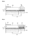
- FIG. 3 is a cross-sectional view of the display filter according to the first embodiment
- FIG. 4 illustrates a plasma display apparatus according to a second embodiment
- FIG. 5 illustrates a plasma display apparatus according to a third embodiment
- FIG. 6 illustrates the display filter and a ground member in the plasma display apparatus according to the first embodiment
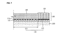
- FIG. 7 illustrates a plasma display apparatus according to a fourth embodiment.
- a display filter comprises an electromagnetic interference shielding layer, one or more films contacting the electromagnetic interference shielding layer, and a conductive layer filled in a through hole formed in the one or more films.
- the one or more films may be formed on the electromagnetic interference shielding layer.
- the display filter may comprise a film filter.
- the one or more films may be an anti-reflection layer.
- the display filter may further comprise an anti-reflection layer.
- the through hole may be formed in a partial area of the one or more films which does not overlap the anti-reflection layer.
- the conductive layer may comprise silver or copper.
- the electromagnetic interference shielding layer may comprise a mesh portion.
- the display filter may further comprise a near-infrared ray shielding layer.
- the display filter may further comprise a color correction layer.
- the display filter may further comprise a layer having both a near-infrared ray shielding function and a color correction function.
- the diameter of the through hole may range from 1 mm to 5 mm.
- the length of the through hole may be equal to or less than the length of the conductive layer.
- a plasma display apparatus comprises a plasma display panel, a display filter, formed on the plasma display panel, comprising an electromagnetic interference shielding layer, one or more films contacting the electromagnetic interference shielding layer, and a conductive layer filled in a through hole formed in the one or more films, and a ground member connected to the conductive layer.
- the ground member may comprise a finger spring.
- the ground member may comprise an anisotropic conductive film or a conductive adhesive.
- the display filter may further comprise an anti-reflection layer.
- the through hole may be formed in a partial area of the one or more films which does not overlap the anti-reflection layer.
- the diameter of the through hole may range from 1 mm to 5 mm.
- a display filter comprises an electromagnetic interference shielding layer, and one or more films contacting the electromagnetic interference shielding layer and having a through hole.
- the diameter of the through hole may range from 1 mm to 5 mm.
- FIG. 1 illustrates a plasma display apparatus according to a first embodiment.
- the plasma display apparatus according to the first embodiment comprises a display filter 100 and a plasma display panel 200.
- the display filter 100 is disposed on an upper surface of the plasma display panel 200.
- the display filter 100 of the plasma display apparatus according to the first embodiment comprises a film filter.
- the display filter 100 comprises an electromagnetic interference shielding layer 110, one or more films 120 contacting the electromagnetic interference shielding layer 110, a conductive layer 130 filled in a through hole formed in the one or more films 120, and an anti-reflection layer 140 formed on the one or more films 120. While the conductive layer 130 is formed in one or more films 120 in FIG. 1, the conductive layer 130 may be formed in a plurality of films which are laminated one another. The through hole passes from an upper surface to a lower surface of the film 120.
- the one or more films 120 are made of a material capable of transmitting light.
- the material capable of transmitting light include cellulose-based resin such as polyethylene terephthalate, polyethersulfone, polystyrene, polyethylene naphthalate, polyaryllate, polyetheretherketone, polycarbonate, polyethylene, polypropylene, polyamide, polyimide, triacetylcellulose, fluorine-based resin such as polyurethane, polytetrafluoroethylene, vinyl compound such as polyvinyl chloride, polyacrylate, polymethacrylate or copolymer thereof
- the thickness of the one or more films 120 may range from 75 ⁇ m to 150 ⁇ m.
- the total thickness of the laminated films may range from 75 ⁇ m to 150 ⁇ m.
- the display filter 100 has strength and flexibility to the extent that the display filter 100 can be formed on the plasma display panel 200.
- the electromagnetic interference shielding layer 110 may comprise a metal with high conductivity such as silver (Ag) or copper (Cu).
- the electromagnetic interference shielding layer 110 may be a mesh type shielding layer or a conductive layer type shielding layer.
- the mesh type shielding layer comprises a mesh portion 111 having a conductive mesh and a metal frame 113 surrounding an outer area of the mesh portion 111.
- the metal frame 113 of the mesh type shielding layer surrounds the outer area of the mesh portion 111, thereby supporting the mesh portion 111.
- the metal frame 113 is electrically connected to the conductive layer 130 filled in the through hole.
- the mesh portion 111 secures transmissivity of light emitted from the plasma display panel 200, and absorbs an electromagnetic wave.
- the electromagnetic interference shielding layer 110 may comprise only the mesh portion. In such a case, the conductive mesh of the mesh portion may contact the conductive layer 130.
- the electromagnetic interference shielding layer 110 may be formed using a sputtering method, an electrolytic plating method, an electroless plating method, and the like.
- a method for forming a copper layer using the electroless plating method comprises adhering metal catalyst for accelerating metal crystal growth on a film 115, and immersing the film 115 in a plating solution including copper salt, a reducing agent, a complexing agent, a pH control agent, a pH buffer agent and an improvement agent.
- the metal catalyst comprises silver (Ag) or palladium (Pd).
- the copper salt functions as the supplying of copper ions to the film 115.
- the copper salt may comprise Ag-Cu chloride, nitrates, sulfate.
- the reducing agent functions as the reduction of metal ions on the film 115.
- the reducing agent comprises polysaccharide compound such as NaBH 4 , KBH 4 , hydrazine, formalin or glucose.
- the complexing agent prevents the precipitation of hydroxide in an alkaline solution, and controls a concentration of free metal ions, thereby preventing the decomposition of metal salt and controlling a plating speed.
- the complexing agent comprises a chelate agent such as an ammonia solution, acetic acid, guanine acid, stannate, EDTA, or an organic amine compound.
- the pH control agent controls pH of the plating solution.
- the pH control agent comprises an acid compound or a base compound.
- the pH buffer agent prevents a change in pH, and comprises various organic acids or a weak acid inorganic compound.
- the improvement agent improves a coating characteristic and a planarization characteristic.
- the improvement agent comprises surfactant or an adsorbent material capable of adsorbing a component for interrupting the crystal growth.
- a method for forming a silver layer using the electroless plating method comprises immersing the film 115 in a plating solution including a silver salt, a reducing agent, a complexing agent, a pH control agent, a pH buffer agent and an improvement agent.
- a plating solution including a silver salt, a reducing agent, a complexing agent, a pH control agent, a pH buffer agent and an improvement agent.
- a photoresist pattern of the conductive mesh is formed on the metal layer using a photolithography process. Then, the metal layer is etched using the photoresist pattern of the conductive mesh as a mask, thereby forming the mesh portion 111 and the metal frame 113.
- the mesh portion 111 comprises a conductive mesh 111a having the cross structure.
- the mesh portion 111 has holes inclined to a bias angle capable of transmitting visible light by the conductive mesh 111a.
- the bias angle may vary depending on definition of the plasma display panel 200.
- the anti-reflection layer 140 may have refractive index equal to or less than 1.5 in a visible region.
- the anti-reflection layer 140 may have refractive index equal to or less than 1.4, and may be formed of fluorine-based transparent polymer resin being a single layer, silicon-based resin, a silicon oxide thin film, and the like. Further, the anti-reflection layer 140 may be formed by laminating a layer with high refractive index and a layer with low refractive index.
- the layer with high refractive index and the layer with low refractive index each comprise an inorganic compound such as a metal oxide, fluoride, silicide, boride, carbide, nitride, sulfide, or an organic compound such as silicon-based resin, acrylic-based resin.
- an inorganic compound such as a metal oxide, fluoride, silicide, boride, carbide, nitride, sulfide, or an organic compound such as silicon-based resin, acrylic-based resin.
- the anti-reflection layer being a single layer is easy to be manufactured.
- the anti-reflection layer being a plurality of layers has an excellent anti-reflection property, and also has an anti-reflection property throughout a wide wavelength area. Further, the anti-reflection layer of the plurality of layers is slightly affected by an optical design by an optical characteristic of a film.
- the anti-reflection layer 140 of the plurality of layers may have visible light reflectivity of 2%.
- the anti-reflection layer 140 may comprise a hard coating layer.
- the hard coating layer may be formed of thermosetting resin or photo-crosslinked resin such as acrylic-based resin, silicon-based resin, melamine-based resin, urethane-based resin, fluorine-based resin.
- the anti-reflection layer 140 prevents a glare phenomenon generated by reflecting visible light from the outside on the surface of the plasma display panel 200, thereby improving contrast and color purity of the plasma display panel 200.
- FIG. 2 is a plane view of a display filter according to the first embodiment.
- FIG. 3 is a cross-sectional view of the display filter according to the first embodiment.
- the through hole 150 formed in the one ore more films 120 is a space filled with the conductive layer 130 for electrically connecting the electromagnetic interference shielding layer 110 to a ground member (not illustrated).
- the diameter of the through hole may range from 1 mm to 5 mm. When the diameter of the through hole 150 ranges from 1 mm to 5 mm, it is easy to fill the through hole 150 with the conductive layer 130, and the through hole 150 does not interrupt the formation of the electromagnetic interference shielding layer 110. As illustrated in FIGs.
- the through hole 150 may be formed at an edge of the film 120, i.e., in a partial area of the film 120 where the anti-reflection layer 140 is not formed. Accordingly, a length L1 of the through hole 150 may be equal to or less than a length L2 of the conductive layer 130.
- the conductive layer 130 filled in the through hole 140 may comprise silver or copper.
- the conductive layer 130 may be formed inside and outside the through hole 150, i.e., on an upper surface of the film 120.
- the conductive layer 130 may be filled using a method of coating a metal paste or a plating method.
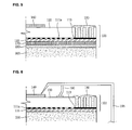
- FIG. 4 illustrates a plasma display apparatus according to a second embodiment. As illustrated in FIG. 4, before filling a through hole 150 with a conductive layer 130, a growth nucleus 160 is formed inside the through hole 150.
- the growth nucleus 160 is formed on the electromagnetic interference shielding layer 110 using a method such as a screen printing method, and a portion of the inside of the through hole 150 is filled with the growth nucleus 160 in a combination process of the electromagnetic interference shielding layer 110 and a film 120.
- the portion of the inside of the through hole 150 is filled with the growth nucleus 160, the formation of the conductive layer 130 using a plating method can be carried out rapidly by the growth nucleus 160.
- FIG. 5 illustrates a plasma display apparatus according to a third embodiment.
- the plasma display apparatus according to the third embodiment may further comprise at least one of a near-infrared ray shielding layer 170 or a color correction layer 180.
- the near-infrared ray shielding layer 170 absorbs near-infrared rays having a wavelength of 800-1,000 nm generated in a plasma display panel 200, thereby normally inputting control infrared rays generated in a remote controller, and the like, of the plasma display apparatus to an infrared ray receiving unit (not illustrated) without the interference of the near-infrared rays.
- the color correction layer 180 comprises a color control dye, thereby improving color purity of the plasma display apparatus.
- the color correction layer may be omitted.
- the laminating order of an anti-reflection layer 140, the near-infrared ray shielding layer 170 and the color correction layer 180 may change.
- the anti-reflection layer 140 may formed under an electromagnetic interference shielding layer 110.
- the electromagnetic interference shielding layer 110, the color correction layer 180 and the near-infrared ray shielding layer 170 may be laminated in the order named.
- FIG. 6 illustrates the display filter and a ground member in the plasma display apparatus according to the first embodiment.
- a ground member 190 electrically connects the conductive layer 130 to a case 195 of the plasma display apparatus.
- the ground member 190 may comprise a finger spring. Further, the ground member 190 may comprise a finger spring, or an anisotropic conductive film or a conductive adhesive instead of the finger spring.
- FIG. 7 illustrates a plasma display apparatus according to a fourth embodiment.
- the plasma display apparatus according to the fourth embodiment comprises an anti-reflection layer 140 having a through hole.
- the through hole 150 illustrated in FIG. 1 is formed in the one ore more films 120 provided separately from the anti-reflection layer 140.
- the through hole according to the fourth embodiment is formed in the anti-reflection layer 140, and the inside of the through hole is filled with a conductive layer 130.
- the conductive layer 130 contacts an electromagnetic interference shielding layer 110.
- the embodiments provide the simple ground structure by filling the through hole with the conductive layer.
Landscapes
- Physics & Mathematics (AREA)
- Engineering & Computer Science (AREA)
- Plasma & Fusion (AREA)
- Electromagnetism (AREA)
- Microelectronics & Electronic Packaging (AREA)
- General Physics & Mathematics (AREA)
- Optics & Photonics (AREA)
- Shielding Devices Or Components To Electric Or Magnetic Fields (AREA)
- Devices For Indicating Variable Information By Combining Individual Elements (AREA)
Abstract
Description
- This document relates to a display filter and a plasma display apparatus.
- A plasma display apparatus comprises a plasma display panel in which a discharge cell is filled with a main discharge gas and an inert gas, and a driver. When a high frequency voltage is supplied to an electrode of the plasma display panel, the inert gas generates vacuum ultraviolet rays, which thereby cause a phosphor formed between barrier ribs of the plasma display panel to emit light.
- The plasma display apparatus displays an image during each of subfields constituting a frame. Each of the subfields comprises a reset period for initializing all the discharge cells, an address period for selecting cells to be discharged and a sustain period for representing gray level in accordance with the number of discharges.
- The reset period comprises a setup period and a set-down period. During the setup period, a setup pulse is supplied to scan electrodes. The setup pulse generates a weak dark discharge in the discharge cells. This results in wall charges of a positive polarity being accumulated on address electrodes and sustain electrodes, and wall charges of a negative polarity being accumulated on the scan electrodes.
- During the set-down period, a set-down pulse is supplied to the scan electrodes. This results in erasing a portion of the wall charges excessively accumulated on the scan electrodes such the remaining wall charges are uniform inside the discharge cells.
- During the address period, a scan pulse is supplied to the scan electrodes, and a data pulse is supplied to the address electrodes. As the voltage difference between the scan pulse and the data pulse is added to the wall voltage produced during the reset period, the cells to be discharged are selected.
- During the sustain period, a sustain pulse is supplied to the scan electrodes and the sustain electrodes. A sustain discharge occurs within the discharge cells selected during the address period, thereby displaying an image.
- The driver of the plasma display apparatus supplies a driving pulse to the electrode of the plasma display panel during the reset period, the address period and the sustain period. In other words, the driver supplies the setup pulse and the set-down pulse during the reset period, the data pulse and the scan pulse during the address period, and the sustain pulse during the sustain period.
- Since the plasma display apparatus displays the image using the high frequency voltage for generating the plasma discharge, an electromagnetic wave is emitted from the front surface of the plasma display panel. Further, the plasma display apparatus emits near-infrared rays by the inert gas. The plasma display apparatus comprises a display filter for reducing or removing the electromagnetic wave emitted from the plasma display panel or the near-infrared rays.
- In one aspect, a display filter comprises an electromagnetic interference shielding layer, one or more films contacting the electromagnetic interference shielding layer, and a conductive layer filled in a through hole formed in the one or more films.
- In another aspect, a plasma display apparatus comprises a plasma display panel, a display filter, formed on the plasma display panel, comprising an electromagnetic interference shielding layer, one or more films contacting the electromagnetic interference shielding layer, and a conductive layer filled in a through hole formed in the one or more films, and a ground member connected to the conductive layer.
- In still another aspect, a display filter comprises an electromagnetic interference shielding layer, and one or more films contacting the electromagnetic interference shielding layer and having a through hole.
- The accompany drawings, which are included to provide a further understanding of the invention and are incorporated on and constitute a part of this specification illustrate embodiments of the invention and together with the description serve to explain the principles of the invention.
- FIG. 1 illustrates a plasma display apparatus according to a first embodiment;
- FIG. 2 is a plane view of a display filter according to the first embodiment;
- FIG. 3 is a cross-sectional view of the display filter according to the first embodiment;
- FIG. 4 illustrates a plasma display apparatus according to a second embodiment;
- FIG. 5 illustrates a plasma display apparatus according to a third embodiment;
- FIG. 6 illustrates the display filter and a ground member in the plasma display apparatus according to the first embodiment; and
- FIG. 7 illustrates a plasma display apparatus according to a fourth embodiment.
- Preferred embodiments of the present invention will be described in a more detailed manner with reference to the drawings.
- A display filter comprises an electromagnetic interference shielding layer, one or more films contacting the electromagnetic interference shielding layer, and a conductive layer filled in a through hole formed in the one or more films.
- The one or more films may be formed on the electromagnetic interference shielding layer.
- The display filter may comprise a film filter.
- The one or more films may be an anti-reflection layer.
- The display filter may further comprise an anti-reflection layer.
- The through hole may be formed in a partial area of the one or more films which does not overlap the anti-reflection layer.
- The conductive layer may comprise silver or copper.
- The electromagnetic interference shielding layer may comprise a mesh portion.
- The display filter may further comprise a near-infrared ray shielding layer.
- The display filter may further comprise a color correction layer.
- The display filter may further comprise a layer having both a near-infrared ray shielding function and a color correction function.
- The diameter of the through hole may range from 1 mm to 5 mm.
- The length of the through hole may be equal to or less than the length of the conductive layer.
- A plasma display apparatus comprises a plasma display panel, a display filter, formed on the plasma display panel, comprising an electromagnetic interference shielding layer, one or more films contacting the electromagnetic interference shielding layer, and a conductive layer filled in a through hole formed in the one or more films, and a ground member connected to the conductive layer.
- The ground member may comprise a finger spring.
- The ground member may comprise an anisotropic conductive film or a conductive adhesive.
- The display filter may further comprise an anti-reflection layer.
- The through hole may be formed in a partial area of the one or more films which does not overlap the anti-reflection layer.
- The diameter of the through hole may range from 1 mm to 5 mm.
- A display filter comprises an electromagnetic interference shielding layer, and one or more films contacting the electromagnetic interference shielding layer and having a through hole.
- The diameter of the through hole may range from 1 mm to 5 mm.
- Hereinafter, exemplary embodiments of the present invention will be described in detail with reference to the attached drawings.
- FIG. 1 illustrates a plasma display apparatus according to a first embodiment. As illustrated in FIG. 1, the plasma display apparatus according to the first embodiment comprises a
display filter 100 and aplasma display panel 200. Thedisplay filter 100 is disposed on an upper surface of theplasma display panel 200. Thedisplay filter 100 of the plasma display apparatus according to the first embodiment comprises a film filter. - The
display filter 100 comprises an electromagneticinterference shielding layer 110, one ormore films 120 contacting the electromagneticinterference shielding layer 110, aconductive layer 130 filled in a through hole formed in the one ormore films 120, and ananti-reflection layer 140 formed on the one ormore films 120. While theconductive layer 130 is formed in one ormore films 120 in FIG. 1, theconductive layer 130 may be formed in a plurality of films which are laminated one another. The through hole passes from an upper surface to a lower surface of thefilm 120. - The one or
more films 120 are made of a material capable of transmitting light. Examples of the material capable of transmitting light include cellulose-based resin such as polyethylene terephthalate, polyethersulfone, polystyrene, polyethylene naphthalate, polyaryllate, polyetheretherketone, polycarbonate, polyethylene, polypropylene, polyamide, polyimide, triacetylcellulose, fluorine-based resin such as polyurethane, polytetrafluoroethylene, vinyl compound such as polyvinyl chloride, polyacrylate, polymethacrylate or copolymer thereof - The thickness of the one or
more films 120 may range from 75 µm to 150 µm. When the plurality of films are laminated, the total thickness of the laminated films may range from 75 µm to 150 µm. When the thickness of the one ormore films 120 ranges from 75 µm to 150 µm, thedisplay filter 100 has strength and flexibility to the extent that thedisplay filter 100 can be formed on theplasma display panel 200. - The electromagnetic
interference shielding layer 110 may comprise a metal with high conductivity such as silver (Ag) or copper (Cu). The electromagneticinterference shielding layer 110 may be a mesh type shielding layer or a conductive layer type shielding layer. The mesh type shielding layer comprises amesh portion 111 having a conductive mesh and ametal frame 113 surrounding an outer area of themesh portion 111. Themetal frame 113 of the mesh type shielding layer surrounds the outer area of themesh portion 111, thereby supporting themesh portion 111. Themetal frame 113 is electrically connected to theconductive layer 130 filled in the through hole. Themesh portion 111 secures transmissivity of light emitted from theplasma display panel 200, and absorbs an electromagnetic wave. The electromagneticinterference shielding layer 110 may comprise only the mesh portion. In such a case, the conductive mesh of the mesh portion may contact theconductive layer 130. - The electromagnetic
interference shielding layer 110 may be formed using a sputtering method, an electrolytic plating method, an electroless plating method, and the like. A method for forming a copper layer using the electroless plating method comprises adhering metal catalyst for accelerating metal crystal growth on afilm 115, and immersing thefilm 115 in a plating solution including copper salt, a reducing agent, a complexing agent, a pH control agent, a pH buffer agent and an improvement agent. - The metal catalyst comprises silver (Ag) or palladium (Pd). The copper salt functions as the supplying of copper ions to the
film 115. For example, the copper salt may comprise Ag-Cu chloride, nitrates, sulfate. The reducing agent functions as the reduction of metal ions on thefilm 115. The reducing agent comprises polysaccharide compound such as NaBH4, KBH4, hydrazine, formalin or glucose. The complexing agent prevents the precipitation of hydroxide in an alkaline solution, and controls a concentration of free metal ions, thereby preventing the decomposition of metal salt and controlling a plating speed. The complexing agent comprises a chelate agent such as an ammonia solution, acetic acid, guanine acid, stannate, EDTA, or an organic amine compound. The pH control agent controls pH of the plating solution. The pH control agent comprises an acid compound or a base compound. The pH buffer agent prevents a change in pH, and comprises various organic acids or a weak acid inorganic compound. The improvement agent improves a coating characteristic and a planarization characteristic. The improvement agent comprises surfactant or an adsorbent material capable of adsorbing a component for interrupting the crystal growth. - A method for forming a silver layer using the electroless plating method comprises immersing the
film 115 in a plating solution including a silver salt, a reducing agent, a complexing agent, a pH control agent, a pH buffer agent and an improvement agent. Components and functions of the components of the plating solution were described above. - When a metal layer is formed on an upper surface of the film, a photoresist pattern of the conductive mesh is formed on the metal layer using a photolithography process. Then, the metal layer is etched using the photoresist pattern of the conductive mesh as a mask, thereby forming the
mesh portion 111 and themetal frame 113. - The
mesh portion 111 comprises aconductive mesh 111a having the cross structure. Themesh portion 111 has holes inclined to a bias angle capable of transmitting visible light by theconductive mesh 111a. The bias angle may vary depending on definition of theplasma display panel 200. - The
anti-reflection layer 140 may have refractive index equal to or less than 1.5 in a visible region. For example, theanti-reflection layer 140 may have refractive index equal to or less than 1.4, and may be formed of fluorine-based transparent polymer resin being a single layer, silicon-based resin, a silicon oxide thin film, and the like. Further, theanti-reflection layer 140 may be formed by laminating a layer with high refractive index and a layer with low refractive index. The layer with high refractive index and the layer with low refractive index each comprise an inorganic compound such as a metal oxide, fluoride, silicide, boride, carbide, nitride, sulfide, or an organic compound such as silicon-based resin, acrylic-based resin. - The anti-reflection layer being a single layer is easy to be manufactured. The anti-reflection layer being a plurality of layers has an excellent anti-reflection property, and also has an anti-reflection property throughout a wide wavelength area. Further, the anti-reflection layer of the plurality of layers is slightly affected by an optical design by an optical characteristic of a film. The
anti-reflection layer 140 of the plurality of layers may have visible light reflectivity of 2%. - Since the
anti-reflection layer 140 is exposed to the outside, theanti-reflection layer 140 may comprise a hard coating layer. The hard coating layer may be formed of thermosetting resin or photo-crosslinked resin such as acrylic-based resin, silicon-based resin, melamine-based resin, urethane-based resin, fluorine-based resin. - The
anti-reflection layer 140 prevents a glare phenomenon generated by reflecting visible light from the outside on the surface of theplasma display panel 200, thereby improving contrast and color purity of theplasma display panel 200. - FIG. 2 is a plane view of a display filter according to the first embodiment. FIG. 3 is a cross-sectional view of the display filter according to the first embodiment. The through
hole 150 formed in the one oremore films 120 is a space filled with theconductive layer 130 for electrically connecting the electromagneticinterference shielding layer 110 to a ground member (not illustrated). The diameter of the through hole may range from 1 mm to 5 mm. When the diameter of the throughhole 150 ranges from 1 mm to 5 mm, it is easy to fill the throughhole 150 with theconductive layer 130, and the throughhole 150 does not interrupt the formation of the electromagneticinterference shielding layer 110. As illustrated in FIGs. 2 and 3, the throughhole 150 may be formed at an edge of thefilm 120, i.e., in a partial area of thefilm 120 where theanti-reflection layer 140 is not formed. Accordingly, a length L1 of the throughhole 150 may be equal to or less than a length L2 of theconductive layer 130. - As illustrated in FIG. 1, the
conductive layer 130 filled in the throughhole 140 may comprise silver or copper. To stably ground using theconductive layer 130, theconductive layer 130 may be formed inside and outside the throughhole 150, i.e., on an upper surface of thefilm 120. Theconductive layer 130 may be filled using a method of coating a metal paste or a plating method. - FIG. 4 illustrates a plasma display apparatus according to a second embodiment. As illustrated in FIG. 4, before filling a through
hole 150 with aconductive layer 130, agrowth nucleus 160 is formed inside the throughhole 150. - When the through
hole 150 is previously formed before forming an electromagneticinterference shielding layer 110, thegrowth nucleus 160 is formed on the electromagneticinterference shielding layer 110 using a method such as a screen printing method, and a portion of the inside of the throughhole 150 is filled with thegrowth nucleus 160 in a combination process of the electromagneticinterference shielding layer 110 and afilm 120. When the portion of the inside of the throughhole 150 is filled with thegrowth nucleus 160, the formation of theconductive layer 130 using a plating method can be carried out rapidly by thegrowth nucleus 160. - FIG. 5 illustrates a plasma display apparatus according to a third embodiment. As illustrated in FIG. 5, the plasma display apparatus according to the third embodiment may further comprise at least one of a near-infrared ray shielding layer 170 or a color correction layer 180.
- The near-infrared ray shielding layer 170 absorbs near-infrared rays having a wavelength of 800-1,000 nm generated in a
plasma display panel 200, thereby normally inputting control infrared rays generated in a remote controller, and the like, of the plasma display apparatus to an infrared ray receiving unit (not illustrated) without the interference of the near-infrared rays. - The color correction layer 180 comprises a color control dye, thereby improving color purity of the plasma display apparatus. When the near-infrared ray shielding layer has a color correction function, the color correction layer may be omitted.
- In FIG. 5, the laminating order of an
anti-reflection layer 140, the near-infrared ray shielding layer 170 and the color correction layer 180 may change. For example, theanti-reflection layer 140 may formed under an electromagneticinterference shielding layer 110. Further, the electromagneticinterference shielding layer 110, the color correction layer 180 and the near-infrared ray shielding layer 170 may be laminated in the order named. - FIG. 6 illustrates the display filter and a ground member in the plasma display apparatus according to the first embodiment. As illustrated in FIG. 6, a
ground member 190 electrically connects theconductive layer 130 to acase 195 of the plasma display apparatus. Theground member 190 may comprise a finger spring. Further, theground member 190 may comprise a finger spring, or an anisotropic conductive film or a conductive adhesive instead of the finger spring. - FIG. 7 illustrates a plasma display apparatus according to a fourth embodiment. As illustrated in FIG. 7, the plasma display apparatus according to the fourth embodiment comprises an
anti-reflection layer 140 having a through hole. On the other hand, the throughhole 150 illustrated in FIG. 1 is formed in the one oremore films 120 provided separately from theanti-reflection layer 140. In other words, the through hole according to the fourth embodiment is formed in theanti-reflection layer 140, and the inside of the through hole is filled with aconductive layer 130. Theconductive layer 130 contacts an electromagneticinterference shielding layer 110. - The embodiments provide the simple ground structure by filling the through hole with the conductive layer.
- The foregoing embodiments and advantages are merely exemplary and are not to be construed as limiting the present invention. The present teaching can be readily applied to other types of apparatuses. The description of the foregoing embodiments is intended to be illustrative, and not to limit the scope of the claims. Many alternatives, modifications, and variations will be apparent to those skilled in the art. In the claims, means-plus-function clauses are intended to cover the structures described herein as performing the recited function and not only structural equivalents but also equivalent structures. Moreover, unless the term "means" is explicitly recited in a limitation of the claims, such limitation is not intended to be interpreted under 35 USC 112(6).
Claims (21)
- A display filter comprising:an electromagnetic interference shielding layer;one or more films contacting the electromagnetic interference shielding layer; anda conductive layer filled in a through hole formed in the one or more films.
- The display filter of claim 1, wherein the one or more films are formed on the electromagnetic interference shielding layer.
- The display filter of claim 1, wherein the display filter comprises a film filter.
- The display filter of claim 1, wherein the one or more films are an anti-reflection layer.
- The display filter of claim 1, further comprising an anti-reflection layer.
- The display filter of claim 5, wherein the through hole is formed in a partial area of the one or more films which does not overlap the anti-reflection layer.
- The display filter of claim 1, wherein the conductive layer comprises silver or copper.
- The display filter of claim 1, wherein the electromagnetic interference shielding layer comprises a mesh portion.
- The display filter of claim 1, further comprising a near-infrared ray shielding layer.
- The display filter of claim 1, further comprising a color correction layer.
- The display filter of claim 1, further comprising a layer having both a near-infrared ray shielding function and a color correction function.
- The display filter of claim 1, wherein the diameter of the through hole ranges from 1 mm to 5 mm.
- The display filter of claim 1, wherein the length of the through hole is equal to or less than the length of the conductive layer.
- A plasma display apparatus comprising:a plasma display panel;a display filter, formed on the plasma display panel, comprising an electromagnetic interference shielding layer, one or more films contacting the electromagnetic interference shielding layer, and a conductive layer filled in a through hole formed in the one or more films;
anda ground member connected to the conductive layer. - The plasma display apparatus of claim 14, wherein the ground member comprises a finger spring.
- The plasma display apparatus of claim 14, wherein the ground member comprises an anisotropic conductive film or a conductive adhesive.
- The plasma display apparatus of claim 14, wherein the display filter further comprises an anti-reflection layer.
- The plasma display apparatus of claim 17, wherein the through hole is formed in a partial area of the one or more films which does not overlap the anti-reflection layer.
- The plasma display apparatus of claim 14, wherein the diameter of the through hole ranges from 1 mm to 5 mm.
- A display filter comprising:an electromagnetic interference shielding layer, andone or more films contacting the electromagnetic interference shielding layer and having a through hole.
- The display filter of claim 20, wherein the diameter of the through hole ranges from 1 mm to 5 mm.
Applications Claiming Priority (1)
| Application Number | Priority Date | Filing Date | Title |
|---|---|---|---|
| KR1020050095514A KR100731862B1 (en) | 2005-10-11 | 2005-10-11 | Film filter and plasma display panel using the same |
Publications (1)
| Publication Number | Publication Date |
|---|---|
| EP1775605A1 true EP1775605A1 (en) | 2007-04-18 |
Family
ID=37487642
Family Applications (1)
| Application Number | Title | Priority Date | Filing Date |
|---|---|---|---|
| EP06291580A Withdrawn EP1775605A1 (en) | 2005-10-11 | 2006-10-10 | Display filter and plasma display apparatus |
Country Status (5)
| Country | Link |
|---|---|
| US (1) | US20070080643A1 (en) |
| EP (1) | EP1775605A1 (en) |
| JP (1) | JP2007110124A (en) |
| KR (1) | KR100731862B1 (en) |
| CN (1) | CN1949438A (en) |
Cited By (1)
| Publication number | Priority date | Publication date | Assignee | Title |
|---|---|---|---|---|
| EP2204676A1 (en) * | 2008-12-30 | 2010-07-07 | Samsung SDI Co., Ltd. | Optical filter and flat display panel having the same |
Families Citing this family (7)
| Publication number | Priority date | Publication date | Assignee | Title |
|---|---|---|---|---|
| JP2008276220A (en) * | 2007-04-27 | 2008-11-13 | Samsung Sdi Co Ltd | Filter and plasma display device |
| KR100911008B1 (en) * | 2007-05-31 | 2009-08-05 | 삼성에스디아이 주식회사 | Film filter and plasma display device having same |
| JP2009026815A (en) * | 2007-07-17 | 2009-02-05 | Dainippon Printing Co Ltd | Electromagnetic wave shielding sheet and optical filter |
| KR100965376B1 (en) * | 2007-08-24 | 2010-06-22 | 삼성코닝정밀소재 주식회사 | Electromagnetic shielding member for display device |
| KR100975200B1 (en) * | 2008-02-29 | 2010-08-10 | 삼성에스디아이 주식회사 | Single sheet type film filter and manufacturing method thereof and plasma display device using same |
| KR101082446B1 (en) | 2008-12-30 | 2011-11-11 | 삼성에스디아이 주식회사 | Optical Filter and Display Device Comprising the Same |
| CN101915952A (en) * | 2010-07-27 | 2010-12-15 | 中国航空工业集团公司北京航空材料研究院 | Single-layer screen-attached type plasma display flexible light filter and manufacturing method thereof |
Citations (4)
| Publication number | Priority date | Publication date | Assignee | Title |
|---|---|---|---|---|
| EP1267318A1 (en) * | 2000-02-01 | 2002-12-18 | Mitsui Chemicals, Inc. | Filter for displaying, display unit and production method therefor |
| EP1283106A1 (en) * | 2001-03-15 | 2003-02-12 | Mitsui Chemicals, Inc. | Laminated body and display device using the laminated body |
| EP1482331A1 (en) * | 2003-05-28 | 2004-12-01 | Lg Electronics Inc. | Optical filter for a plasma display panel and fabrication method thereof |
| WO2005057606A1 (en) * | 2003-12-10 | 2005-06-23 | Lg Chem, Ltd. | Method for making film assy used in pdpfilter, film assy manufactured by the method, and pdp filter with the film assy |
Family Cites Families (3)
| Publication number | Priority date | Publication date | Assignee | Title |
|---|---|---|---|---|
| KR100513642B1 (en) * | 2002-02-05 | 2005-09-07 | 에스케이씨 주식회사 | Optical filter for plasma display panel and manufacturing method thereof |
| KR20040085699A (en) * | 2003-04-01 | 2004-10-08 | 엘지전자 주식회사 | Front filter of plasma display panel |
| KR20050076458A (en) * | 2004-01-20 | 2005-07-26 | 엘지전자 주식회사 | Grounding method for film filter in plasma display panel |
-
2005
- 2005-10-11 KR KR1020050095514A patent/KR100731862B1/en not_active Expired - Fee Related
-
2006
- 2006-10-10 EP EP06291580A patent/EP1775605A1/en not_active Withdrawn
- 2006-10-11 US US11/548,582 patent/US20070080643A1/en not_active Abandoned
- 2006-10-11 JP JP2006277656A patent/JP2007110124A/en not_active Withdrawn
- 2006-10-11 CN CNA2006101321486A patent/CN1949438A/en active Pending
Patent Citations (4)
| Publication number | Priority date | Publication date | Assignee | Title |
|---|---|---|---|---|
| EP1267318A1 (en) * | 2000-02-01 | 2002-12-18 | Mitsui Chemicals, Inc. | Filter for displaying, display unit and production method therefor |
| EP1283106A1 (en) * | 2001-03-15 | 2003-02-12 | Mitsui Chemicals, Inc. | Laminated body and display device using the laminated body |
| EP1482331A1 (en) * | 2003-05-28 | 2004-12-01 | Lg Electronics Inc. | Optical filter for a plasma display panel and fabrication method thereof |
| WO2005057606A1 (en) * | 2003-12-10 | 2005-06-23 | Lg Chem, Ltd. | Method for making film assy used in pdpfilter, film assy manufactured by the method, and pdp filter with the film assy |
Cited By (2)
| Publication number | Priority date | Publication date | Assignee | Title |
|---|---|---|---|---|
| EP2204676A1 (en) * | 2008-12-30 | 2010-07-07 | Samsung SDI Co., Ltd. | Optical filter and flat display panel having the same |
| US8503123B2 (en) | 2008-12-30 | 2013-08-06 | Samsung Sdi Co., Ltd. | Optical filter and flat display panel comprising the same |
Also Published As
| Publication number | Publication date |
|---|---|
| CN1949438A (en) | 2007-04-18 |
| JP2007110124A (en) | 2007-04-26 |
| KR100731862B1 (en) | 2007-06-25 |
| US20070080643A1 (en) | 2007-04-12 |
| KR20070040141A (en) | 2007-04-16 |
Similar Documents
| Publication | Publication Date | Title |
|---|---|---|
| EP1826804A1 (en) | Display filter and display apparatus having the same | |
| EP1465227B1 (en) | Front filter including an EMI shielding film for a flat panel display device | |
| EP2085812A2 (en) | Film Filter for a Flat Panel Display | |
| US20040214023A1 (en) | Electromagnetic wave shielding filter and method of manufacturing the same | |
| JP4214140B2 (en) | Electromagnetic wave shielding film and method for producing the same | |
| US7612489B2 (en) | Display filter, display device including the display filter, and method of manufacturing the display filter | |
| US20070289774A1 (en) | Electromagnetic interference shielding filter and manufacturing method thereof | |
| JP2008186021A (en) | Filter for display device and display device including the same | |
| CN100474489C (en) | Display equipment with plasma display panel (PDP) | |
| EP1775605A1 (en) | Display filter and plasma display apparatus | |
| JP2005202410A (en) | Filter assembly and manufacturing method thereof, and plasma display panel employing the same | |
| US20070075641A1 (en) | Plasma display apparatus | |
| US6506090B2 (en) | Display panel and method of manufacturing electromagnetic-wave shielding and light transmitting plate | |
| KR20060045104A (en) | Plasma display panel | |
| US20060267499A1 (en) | Plasma display panel (PDP) | |
| JP2006350324A (en) | Direct-attached MRT film filter and plasma display device including the same | |
| KR100629861B1 (en) | Manufacturing method of base film unit for electromagnetic wave filter and base film unit for electromagnetic wave filter manufactured by the manufacturing method | |
| KR100579329B1 (en) | Plasma display device | |
| US20070085458A1 (en) | PDP filter and method of manufacturing the same | |
| KR20090080814A (en) | Plasma display device provided with an optical filter, its manufacturing method, and an optical filter | |
| KR101072430B1 (en) | Conducting member, filter assembly for display device and display device having the same | |
| KR20090012921A (en) | Electromagnetic wave shielding film with excellent light transmittance, direct-attach film filter and plasma display module having the same | |
| EP1635320A2 (en) | Plasma display apparatus and manufacturing method thereof | |
| KR20070052520A (en) | Display device filter and plasma display panel having same | |
| KR20070014436A (en) | MRT film filter attached directly and plasma display device having same |
Legal Events
| Date | Code | Title | Description |
|---|---|---|---|
| PUAI | Public reference made under article 153(3) epc to a published international application that has entered the european phase |
Free format text: ORIGINAL CODE: 0009012 |
|
| AK | Designated contracting states |
Kind code of ref document: A1 Designated state(s): AT BE BG CH CY CZ DE DK EE ES FI FR GB GR HU IE IS IT LI LT LU LV MC NL PL PT RO SE SI SK TR |
|
| AX | Request for extension of the european patent |
Extension state: AL BA HR MK YU |
|
| 17P | Request for examination filed |
Effective date: 20071018 |
|
| 17Q | First examination report despatched |
Effective date: 20071116 |
|
| AKX | Designation fees paid |
Designated state(s): DE FR GB NL |
|
| STAA | Information on the status of an ep patent application or granted ep patent |
Free format text: STATUS: THE APPLICATION IS DEEMED TO BE WITHDRAWN |
|
| 18D | Application deemed to be withdrawn |
Effective date: 20090623 |