EP1774641B1 - Convertisseur de tension miniature monolithique a tres faible tension d'entree - Google Patents
Convertisseur de tension miniature monolithique a tres faible tension d'entree Download PDFInfo
- Publication number
- EP1774641B1 EP1774641B1 EP20050789993 EP05789993A EP1774641B1 EP 1774641 B1 EP1774641 B1 EP 1774641B1 EP 20050789993 EP20050789993 EP 20050789993 EP 05789993 A EP05789993 A EP 05789993A EP 1774641 B1 EP1774641 B1 EP 1774641B1
- Authority
- EP
- European Patent Office
- Prior art keywords
- converter
- voltage
- forming
- energy reservoir
- threshold
- Prior art date
- Legal status (The legal status is an assumption and is not a legal conclusion. Google has not performed a legal analysis and makes no representation as to the accuracy of the status listed.)
- Expired - Lifetime
Links
Images


Classifications
-
- H—ELECTRICITY
- H02—GENERATION; CONVERSION OR DISTRIBUTION OF ELECTRIC POWER
- H02M—APPARATUS FOR CONVERSION BETWEEN AC AND AC, BETWEEN AC AND DC, OR BETWEEN DC AND DC, AND FOR USE WITH MAINS OR SIMILAR POWER SUPPLY SYSTEMS; CONVERSION OF DC OR AC INPUT POWER INTO SURGE OUTPUT POWER; CONTROL OR REGULATION THEREOF
- H02M1/00—Details of apparatus for conversion
- H02M1/36—Means for starting or stopping converters
Definitions
- the invention relates to the field of converters with low input voltage, low power.
- the invention also relates to the field of analog monolithic integrated circuits for electronics, and more particularly to so-called switching voltage converters: these are devices which, connected to a source of variable voltage over a wide range, for example of 0.5 V to 15 V, are able to generate a fixed regulated voltage, for example 3.3 V, for the supply of electronic circuits.
- Applications of low-voltage converters include the power supply of so-called communicating objects and nomadic objects.
- These converters provide suitable voltages for the supply of electronic circuits from different configurations of batteries or batteries.
- SII-IC see http://www.sii-ic.com/).
- Another problem is to be able to use these sources until almost complete discharge, and in any case less than 0.9 V.
- the threshold voltage for the operation of known converters comes from the physics of active devices implanted in integrated circuits (MOS type transistors).
- the invention relates to a DC voltage conversion device as defined in claim 1.
- the voltage of this tank can be coupled to means, for example an electronic architecture, to "start” the converter.
- the converter can, in turn, after starting, recharge the energy reservoir with its output voltage greater than the voltage of the energy tank.
- low input voltages for example between 10 mV and 0.1 V or 0.5 V to be able to start a converter, these low input voltages being compensated by the supply of the reservoir energy or complementary energy supply means.
- the converter will, in turn, be able to generate a fixed regulated voltage, for example 3.3 V, for the supply of electronic circuits.
- the invention also proposes a watch circuit comprising means for comparing an input voltage with a threshold value, means for activating the comparison means, and means for maintaining the level of the result of the comparison when the comparison means are disabled.
- the standby circuit preferably has an extremely low power consumption, in case the converter should remain in the standby position for a long time.
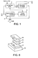
- Block 2 "dc / dc converter” comprises an up-converter filter, for example in pulse modulation.
- Means 4 form a watch circuit for a threshold detection.
- If not are implemented means 7 internal supply, or forming energy reservoir, for example a battery or an internal micro-battery.
- Vbatt or Vdd indicates that the converter 2 is powered either by means 7 or by Vdd, the selection being made using switching means.
- Vout usable externally by an external electronic circuit.
- This voltage supplied by the converter can also be used internally, for example to recharge the means 7 for their next use, especially if they were discharged during startup of the converter 2.
- This recharging can be done using means 8 charge control.
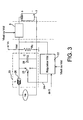
- standby circuit means 4 is illustrated on the figure 2 .
- These means are powered by the input voltage supplied by the means 7 or by the output voltage Vdd.
- This threshold is the minimum operating voltage (40 mV for example).
- this circuit 4 did not exist one could be in a situation where the means 7 (the energy reservoir) would be completely discharged and the system could then only start for input voltages Ve greater than, for example, example, 0.8 V.
- the monitoring of the input voltage can be done in a sampled or periodic manner.
- the idle circuit comprises means 12 which make it possible, by means of a comparator 121, to compare the input voltage Ve with a reference voltage VREF supplied by means 120 generating such a reference voltage . This comparison can be periodically activated by an ACT activation signal.
- the means 4 produce a trigger signal S of the converter 2, for example by means of the control of the clock 6 ( figure 1 ).
- the converter 2 is then powered directly by the voltage reserve 7.
- the means 4 allow the reservoir 7 to deliver its voltage only when the input voltage Ve is above this threshold value.
- the crossing of the threshold value indicates an increase in the input voltage, a criterion according to which the power supply of the converter can be reasonably triggered by the means 7.
- Vdd generated by the converter 2 during operation exceeds another threshold value, for example about 1 Volt.
- the means 10 generate an activation signal ACT.
- These means 10 include, for example, means 101 generating a current reference, means 102 oscillators and means 103 for shaping the ACT signal.
- Means 14 make it possible to maintain the level of the result of the comparison when the means 12 are deactivated, in particular between two ACT activation signals.
- These means comprise, for example, a digital flip-flop, for example a flip-flop D.
- the means 10 and 14 can operate continuously; they are then preferably designed so as to consume as little as possible.
- a current of the order of a few tens of nanoamperes makes it possible to generate the activation signal ACT, under 2V, and to maintain the level of current consumption (in the means 14) at approximately some nano-amps, which is compatible with the use of a micro-battery 7 power supply as a reservoir of energy.
- the authorized consumption for the means 12 of comparison is even lower than the activation of this block is frequent.
- comparing means 12 can consume 2 ⁇ A and be activated for one second every hour.
- the figure 3 represents an embodiment of the converter means 2 and the charging means 8.
- the means 2 converters may comprise means 20 forming a lift filter with means 22 for regulating Vdd (for example control means by pulse modulation or pulse density control associated with a PID control type Proportional Integral Derivative ").
- the means 22 may send, via the means 24, a signal to a switch 25, which signal will close or open this switch.
- the means 20 further comprise an inductor 26 L and a capacitor 28 C, these two components being external.
- the compostant Rc represents an external circuit to supply with the output voltage Vdd of the converter means 20.
- a clock signal formed by clock circuit means 6 ( figure 1 ) is supplied to the control means 22 under the control of the means 4, as explained above.
- This clock signal makes it possible to trigger the means 22, and thus the power supply of the converter either with the external voltage Ve or with the voltage of the means 7.
- the regulator 22 makes it possible to reach the desired voltage. It can also advantageously, when Vdd reaches a threshold S 2 predefined, disconnect the means 7, the DC / DC converter is then powered by V DD .
- the means 8 are charging means, in current, means 7, for example a micro-battery during operation of the device.
- the means 8 are adapted to the maximum current available at the output. Indeed, like any electronic circuit, they are designed to work under pre-established conditions: they are said to be "adapted". They include, for example, a current mirror.
- Vbatt or Vdd indicates that the means 8, 22 are powered either by the means 7 or by Vdd, the selection being made using switching means.
- a device such as that of figure 1 uses energy reserve means 7 for starting the converter means if the input voltage Ve is insufficient.
- they can then be recharged by the latter, whose output voltage Vdd is higher than its input voltage.
- These means 7 are for example a battery, or a micro-battery, as in the example illustrated above in connection with the figure 3 .
- a micro-battery can be realized using methods comparable to those presented for example on http://www.cea-technologies.com/energie/67-201. html . Such methods make it possible to produce batteries which supply a voltage of 2 to 2.5 V.
- Such a micro-battery is for example represented on the figure 6 .
- the layer comprises a silicon substrate 50, a platinum current collector 52, a titanium sulfide electrode 54, a LIPON ("lithium phosphate oxynitride”) electrolyte 55 and a lithium metal electrode 56.
- the layers are deposited by PVD technique on the substrate and total about 10 micrometers thick. On the surface, the micro-battery is about a few mm2.
- the battery can be an integral part of the manufacturing process of the integrated circuit; it is invisible to the user.
- the means 7 may, by construction (for example by choice of the materials of the architecture), be made in such a way as to have a negligible self-discharge rate.
- the latter triggers the operation of the converter 2 if, and only if, there is a voltage Ve usable at its input, or uses the energy reservoir 7 to start the converter.
- the reservoir 7 of energy is then charged to start the converter, if the input voltage Ve is insufficient, for example taking into account the comparison made by the means 12 described above.
- the means 7 can be loaded at the moment when the circuit is set up, for example on an electronic card, and at any convenient moment, either by starting the converter 2 with an input voltage Ve sufficient to exceed the threshold, and thus ensure the recharge of the means 7 by the output voltage of said converter, or by a specific charging input. This operation is all the more limited in time as the battery can be recharged quickly.
- the starting voltage of the means 2 can be delivered by something other than a battery, for example by a mechanical converter (for example by a compressed spring).
- the energy reservoir is for example a battery or a micro-battery, and is preferably rechargeable.
- the device may comprise, as explained above, a charging system powered by the output voltage of the converter.
- the battery or micro-battery is preferably integrated.
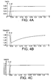
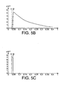
- the Figures 4A-4D represent the temporal evolution of the voltages, respectively, of the input voltage Ve, of the voltage at the terminals of the supply means 7, of the supply voltage generated to the outside, of the supply voltage of the means 4 and means 2 (means of standby and converter).
- the invention therefore proposes a new device, for example of the monolithic integrated circuit type, making it possible to convert the voltage of energy sources towards a voltage usable by electronic circuits, capable of operating with extremely low input voltages, up to a few tens of mV.
- the invention allows the use of new energy sources, not used until now because of their low voltage.
- the device according to the invention is compatible with the integrated circuit industry; it can be integrated in the manufacturing process: the designer of electronic circuits does not have to worry about the assembly of new circuits more or less esoteric or difficult to implement.
- the invention does not increase the volume usually devolved to the function of the voltage conversion.
- the invention makes it possible to provide designers, and in particular electronics engineers, with a DC / DC converter that can handle extremely low input voltages, up to a few tens of mV.
- the described embodiment makes it possible to obtain a monolithic integrated circuit, with a architecture and circuits that manage the charging and providing an integrated micro-battery, which provides sufficient voltage to the transistors of a converter to operate.
Landscapes
- Engineering & Computer Science (AREA)
- Power Engineering (AREA)
- Dc-Dc Converters (AREA)
Applications Claiming Priority (2)
| Application Number | Priority Date | Filing Date | Title |
|---|---|---|---|
| FR0451519A FR2873242B1 (fr) | 2004-07-13 | 2004-07-13 | Convertisseur de tension miniature monolithique a tres faible tension d'entree |
| PCT/FR2005/050568 WO2006008423A1 (fr) | 2004-07-13 | 2005-07-11 | Convertisseur de tension miniature monolithique a tres faible tension d'entree |
Publications (2)
| Publication Number | Publication Date |
|---|---|
| EP1774641A1 EP1774641A1 (fr) | 2007-04-18 |
| EP1774641B1 true EP1774641B1 (fr) | 2011-05-11 |
Family
ID=34946782
Family Applications (1)
| Application Number | Title | Priority Date | Filing Date |
|---|---|---|---|
| EP20050789993 Expired - Lifetime EP1774641B1 (fr) | 2004-07-13 | 2005-07-11 | Convertisseur de tension miniature monolithique a tres faible tension d'entree |
Country Status (7)
| Country | Link |
|---|---|
| US (1) | US7642765B2 (enExample) |
| EP (1) | EP1774641B1 (enExample) |
| JP (1) | JP4805925B2 (enExample) |
| AT (1) | ATE509423T1 (enExample) |
| ES (1) | ES2371443T3 (enExample) |
| FR (1) | FR2873242B1 (enExample) |
| WO (1) | WO2006008423A1 (enExample) |
Families Citing this family (5)
| Publication number | Priority date | Publication date | Assignee | Title |
|---|---|---|---|---|
| US8451627B2 (en) | 2007-11-16 | 2013-05-28 | Itron, Inc. | Devices and methods for converting alternating current (AC) power to direct current (DC) power |
| US8773086B1 (en) * | 2007-12-07 | 2014-07-08 | Marvell International Ltd. | Circuits and methods for dynamic voltage management |
| FR2945684B1 (fr) | 2009-05-14 | 2011-06-17 | Commissariat Energie Atomique | Circuit convertisseur et systeme electronique comportant un tel circuit |
| US8773869B2 (en) * | 2010-03-29 | 2014-07-08 | Itron, Inc. | System and method for conversion of high voltage AC to low voltage DC using input voltage gating |
| WO2014091088A1 (fr) | 2012-12-11 | 2014-06-19 | Commissariat A L'energie Atomique Et Aux Energies Alternatives | Circuit de comparaison d'une tension a un seuil et conversion d'energie electrique |
Family Cites Families (12)
| Publication number | Priority date | Publication date | Assignee | Title |
|---|---|---|---|---|
| JPS56145726U (enExample) * | 1980-03-28 | 1981-11-04 | ||
| JPH02280661A (ja) * | 1989-04-21 | 1990-11-16 | Ricoh Co Ltd | 定電圧出力回路 |
| US5338625A (en) * | 1992-07-29 | 1994-08-16 | Martin Marietta Energy Systems, Inc. | Thin film battery and method for making same |
| JPH0779562A (ja) * | 1993-09-09 | 1995-03-20 | Canon Inc | Dc/dcコンバータ |
| US6351073B1 (en) * | 1999-11-10 | 2002-02-26 | Thomas & Betts International, Inc. | Self-supplied DC/DC switching power supply |
| FR2814264B1 (fr) * | 2000-09-20 | 2002-10-25 | Commissariat Energie Atomique | Dispositif electronique integre securise |
| US6655035B2 (en) * | 2000-10-20 | 2003-12-02 | Continuum Photonics, Inc. | Piezoelectric generator |
| JP3637876B2 (ja) * | 2001-04-05 | 2005-04-13 | トヨタ自動車株式会社 | Dc−dcコンバータの制御装置 |
| EP1387479A1 (en) * | 2002-08-02 | 2004-02-04 | Dialog Semiconductor GmbH | Digital controlled charge current regulator |
| JP2004147409A (ja) * | 2002-10-23 | 2004-05-20 | Canon Inc | 電源装置 |
| US7019506B2 (en) * | 2002-11-14 | 2006-03-28 | Fyre Storm, Inc. | Charge-based switching power converter controller |
| US6969981B1 (en) * | 2003-09-09 | 2005-11-29 | National Semiconductor Corporation | Voltage regulator power management apparatus |
-
2004
- 2004-07-13 FR FR0451519A patent/FR2873242B1/fr not_active Expired - Fee Related
-
2005
- 2005-07-11 WO PCT/FR2005/050568 patent/WO2006008423A1/fr not_active Ceased
- 2005-07-11 US US11/631,526 patent/US7642765B2/en not_active Expired - Fee Related
- 2005-07-11 JP JP2007520868A patent/JP4805925B2/ja not_active Expired - Fee Related
- 2005-07-11 AT AT05789993T patent/ATE509423T1/de not_active IP Right Cessation
- 2005-07-11 ES ES05789993T patent/ES2371443T3/es not_active Expired - Lifetime
- 2005-07-11 EP EP20050789993 patent/EP1774641B1/fr not_active Expired - Lifetime
Also Published As
| Publication number | Publication date |
|---|---|
| WO2006008423A1 (fr) | 2006-01-26 |
| JP4805925B2 (ja) | 2011-11-02 |
| JP2008507247A (ja) | 2008-03-06 |
| FR2873242B1 (fr) | 2007-12-21 |
| ES2371443T3 (es) | 2012-01-02 |
| US7642765B2 (en) | 2010-01-05 |
| US20070223255A1 (en) | 2007-09-27 |
| EP1774641A1 (fr) | 2007-04-18 |
| FR2873242A1 (fr) | 2006-01-20 |
| ATE509423T1 (de) | 2011-05-15 |
Similar Documents
| Publication | Publication Date | Title |
|---|---|---|
| EP1417741B1 (fr) | Perfectionnement pour chargeur photovoltaique | |
| EP2393193A1 (fr) | Circuit convertisseur et système électronique comportant un tel circuit | |
| FR2843464A1 (fr) | Circuit de conditionnement d'une source au point de puissance maximum | |
| FR2794578A1 (fr) | Dispositif d'accumulation a batterie | |
| EP3568906B1 (fr) | Dispositif de stockage d'énergie électrique apte à se recharger sous une première tension et à restituer son énergie sous une deuxième tension | |
| FR2910141A1 (fr) | Systeme de generation d'energie electrique avec maximisation de la puissance | |
| EP2430738B1 (fr) | Circuit convertisseur et systeme electronique comportant un tel circuit | |
| FR2970123A1 (fr) | Circuit de protection d'une batterie en couches minces | |
| EP1774641B1 (fr) | Convertisseur de tension miniature monolithique a tres faible tension d'entree | |
| EP2932588B1 (fr) | Circuit de comparaison d'une tension a un seuil et conversion d'energie electrique | |
| EP1094589A1 (fr) | Système de gestion de charge pour batterie d'accumulateurs électriques et notamment d'une batterie composée de cellules au lithium | |
| EP2395594B1 (fr) | Dispositif et procédé d'alimentation pour système de communication sans fil et ensemble capteur comportant un tel dispositif | |
| WO2010063913A2 (fr) | Dispositif d'alimentation électrique, et installation de commande d'un sectionneur incluant un tel dispositif | |
| WO2006067350A1 (fr) | Procede et systeme d'alimentation electrique autonome par energie renouvelable | |
| EP0820139A2 (fr) | Circuit d'alimentation électrique continue régulée par un convertisseur réversible | |
| EP2133977A2 (fr) | Circuit d'alimentation électrique d'une unité de commande d'une installation domotique | |
| EP1905222A2 (fr) | Convertisseur-regulateur continu-continu | |
| FR2492182A1 (fr) | Circuit de commande de la charge d'un accumulateur par une source telle qu'un panneau solaire et generateur comportant un tel circuit | |
| CH721349A2 (fr) | Agencement de circuit pour extraire de l'énergie d'un collecteur d'énergie | |
| FR2961040A1 (fr) | Circuit convertisseur et systeme electronique comportant un tel circuit | |
| CA2528980A1 (fr) | Protection d'une pile a combustible | |
| FR2952484A1 (fr) | Circuit de conversion d'une energie disponible sous une tres faible tension | |
| FR3151162A1 (fr) | Circuit de conversion d'alimentation DC/DC | |
| FR2832869A1 (fr) | Perfectionnement pour chargeur de type photovoltaique | |
| EP1684404A1 (fr) | Circuit convertisseur |
Legal Events
| Date | Code | Title | Description |
|---|---|---|---|
| PUAI | Public reference made under article 153(3) epc to a published international application that has entered the european phase |
Free format text: ORIGINAL CODE: 0009012 |
|
| 17P | Request for examination filed |
Effective date: 20061221 |
|
| AK | Designated contracting states |
Kind code of ref document: A1 Designated state(s): AT BE BG CH CY CZ DE DK EE ES FI FR GB GR HU IE IS IT LI LT LU LV MC NL PL PT RO SE SI SK TR |
|
| DAX | Request for extension of the european patent (deleted) | ||
| RIN1 | Information on inventor provided before grant (corrected) |
Inventor name: DURET, DENIS Inventor name: CONDEMINE, CYRIL Inventor name: LHERMET, HELENE |
|
| RAP1 | Party data changed (applicant data changed or rights of an application transferred) |
Owner name: COMMISSARIAT A L'ENERGIE ATOMIQUE ET AUX ENERGIES |
|
| RIC1 | Information provided on ipc code assigned before grant |
Ipc: H02M 1/36 20070101AFI20100818BHEP |
|
| GRAP | Despatch of communication of intention to grant a patent |
Free format text: ORIGINAL CODE: EPIDOSNIGR1 |
|
| GRAS | Grant fee paid |
Free format text: ORIGINAL CODE: EPIDOSNIGR3 |
|
| GRAA | (expected) grant |
Free format text: ORIGINAL CODE: 0009210 |
|
| AK | Designated contracting states |
Kind code of ref document: B1 Designated state(s): AT BE BG CH CY CZ DE DK EE ES FI FR GB GR HU IE IS IT LI LT LU LV MC NL PL PT RO SE SI SK TR |
|
| REG | Reference to a national code |
Ref country code: GB Ref legal event code: FG4D Free format text: NOT ENGLISH |
|
| REG | Reference to a national code |
Ref country code: CH Ref legal event code: EP |
|
| REG | Reference to a national code |
Ref country code: IE Ref legal event code: FG4D |
|
| REG | Reference to a national code |
Ref country code: DE Ref legal event code: R096 Ref document number: 602005028000 Country of ref document: DE Effective date: 20110622 |
|
| REG | Reference to a national code |
Ref country code: SE Ref legal event code: TRGR |
|
| REG | Reference to a national code |
Ref country code: NL Ref legal event code: VDEP Effective date: 20110511 |
|
| PG25 | Lapsed in a contracting state [announced via postgrant information from national office to epo] |
Ref country code: PT Free format text: LAPSE BECAUSE OF FAILURE TO SUBMIT A TRANSLATION OF THE DESCRIPTION OR TO PAY THE FEE WITHIN THE PRESCRIBED TIME-LIMIT Effective date: 20110912 Ref country code: LT Free format text: LAPSE BECAUSE OF FAILURE TO SUBMIT A TRANSLATION OF THE DESCRIPTION OR TO PAY THE FEE WITHIN THE PRESCRIBED TIME-LIMIT Effective date: 20110511 |
|
| PG25 | Lapsed in a contracting state [announced via postgrant information from national office to epo] |
Ref country code: LV Free format text: LAPSE BECAUSE OF FAILURE TO SUBMIT A TRANSLATION OF THE DESCRIPTION OR TO PAY THE FEE WITHIN THE PRESCRIBED TIME-LIMIT Effective date: 20110511 Ref country code: GR Free format text: LAPSE BECAUSE OF FAILURE TO SUBMIT A TRANSLATION OF THE DESCRIPTION OR TO PAY THE FEE WITHIN THE PRESCRIBED TIME-LIMIT Effective date: 20110812 Ref country code: CY Free format text: LAPSE BECAUSE OF FAILURE TO SUBMIT A TRANSLATION OF THE DESCRIPTION OR TO PAY THE FEE WITHIN THE PRESCRIBED TIME-LIMIT Effective date: 20110511 Ref country code: IS Free format text: LAPSE BECAUSE OF FAILURE TO SUBMIT A TRANSLATION OF THE DESCRIPTION OR TO PAY THE FEE WITHIN THE PRESCRIBED TIME-LIMIT Effective date: 20110911 Ref country code: AT Free format text: LAPSE BECAUSE OF FAILURE TO SUBMIT A TRANSLATION OF THE DESCRIPTION OR TO PAY THE FEE WITHIN THE PRESCRIBED TIME-LIMIT Effective date: 20110511 Ref country code: SI Free format text: LAPSE BECAUSE OF FAILURE TO SUBMIT A TRANSLATION OF THE DESCRIPTION OR TO PAY THE FEE WITHIN THE PRESCRIBED TIME-LIMIT Effective date: 20110511 Ref country code: FI Free format text: LAPSE BECAUSE OF FAILURE TO SUBMIT A TRANSLATION OF THE DESCRIPTION OR TO PAY THE FEE WITHIN THE PRESCRIBED TIME-LIMIT Effective date: 20110511 |
|
| REG | Reference to a national code |
Ref country code: IE Ref legal event code: FD4D |
|
| PG25 | Lapsed in a contracting state [announced via postgrant information from national office to epo] |
Ref country code: NL Free format text: LAPSE BECAUSE OF FAILURE TO SUBMIT A TRANSLATION OF THE DESCRIPTION OR TO PAY THE FEE WITHIN THE PRESCRIBED TIME-LIMIT Effective date: 20110511 |
|
| REG | Reference to a national code |
Ref country code: ES Ref legal event code: FG2A Ref document number: 2371443 Country of ref document: ES Kind code of ref document: T3 Effective date: 20120102 |
|
| BERE | Be: lapsed |
Owner name: COMMISSARIAT A L'ENERGIE ATOMIQUE ET AUX ENERGIES Effective date: 20110731 |
|
| PG25 | Lapsed in a contracting state [announced via postgrant information from national office to epo] |
Ref country code: EE Free format text: LAPSE BECAUSE OF FAILURE TO SUBMIT A TRANSLATION OF THE DESCRIPTION OR TO PAY THE FEE WITHIN THE PRESCRIBED TIME-LIMIT Effective date: 20110511 Ref country code: CZ Free format text: LAPSE BECAUSE OF FAILURE TO SUBMIT A TRANSLATION OF THE DESCRIPTION OR TO PAY THE FEE WITHIN THE PRESCRIBED TIME-LIMIT Effective date: 20110511 Ref country code: IE Free format text: LAPSE BECAUSE OF FAILURE TO SUBMIT A TRANSLATION OF THE DESCRIPTION OR TO PAY THE FEE WITHIN THE PRESCRIBED TIME-LIMIT Effective date: 20110511 |
|
| PG25 | Lapsed in a contracting state [announced via postgrant information from national office to epo] |
Ref country code: MC Free format text: LAPSE BECAUSE OF NON-PAYMENT OF DUE FEES Effective date: 20110731 Ref country code: DK Free format text: LAPSE BECAUSE OF FAILURE TO SUBMIT A TRANSLATION OF THE DESCRIPTION OR TO PAY THE FEE WITHIN THE PRESCRIBED TIME-LIMIT Effective date: 20110511 Ref country code: RO Free format text: LAPSE BECAUSE OF FAILURE TO SUBMIT A TRANSLATION OF THE DESCRIPTION OR TO PAY THE FEE WITHIN THE PRESCRIBED TIME-LIMIT Effective date: 20110511 Ref country code: SK Free format text: LAPSE BECAUSE OF FAILURE TO SUBMIT A TRANSLATION OF THE DESCRIPTION OR TO PAY THE FEE WITHIN THE PRESCRIBED TIME-LIMIT Effective date: 20110511 Ref country code: PL Free format text: LAPSE BECAUSE OF FAILURE TO SUBMIT A TRANSLATION OF THE DESCRIPTION OR TO PAY THE FEE WITHIN THE PRESCRIBED TIME-LIMIT Effective date: 20110511 |
|
| REG | Reference to a national code |
Ref country code: CH Ref legal event code: PL |
|
| PLBE | No opposition filed within time limit |
Free format text: ORIGINAL CODE: 0009261 |
|
| STAA | Information on the status of an ep patent application or granted ep patent |
Free format text: STATUS: NO OPPOSITION FILED WITHIN TIME LIMIT |
|
| 26N | No opposition filed |
Effective date: 20120214 |
|
| PG25 | Lapsed in a contracting state [announced via postgrant information from national office to epo] |
Ref country code: BE Free format text: LAPSE BECAUSE OF NON-PAYMENT OF DUE FEES Effective date: 20110731 Ref country code: CH Free format text: LAPSE BECAUSE OF NON-PAYMENT OF DUE FEES Effective date: 20110731 Ref country code: LI Free format text: LAPSE BECAUSE OF NON-PAYMENT OF DUE FEES Effective date: 20110731 |
|
| REG | Reference to a national code |
Ref country code: DE Ref legal event code: R097 Ref document number: 602005028000 Country of ref document: DE Effective date: 20120214 |
|
| PG25 | Lapsed in a contracting state [announced via postgrant information from national office to epo] |
Ref country code: LU Free format text: LAPSE BECAUSE OF NON-PAYMENT OF DUE FEES Effective date: 20110711 |
|
| PG25 | Lapsed in a contracting state [announced via postgrant information from national office to epo] |
Ref country code: BG Free format text: LAPSE BECAUSE OF FAILURE TO SUBMIT A TRANSLATION OF THE DESCRIPTION OR TO PAY THE FEE WITHIN THE PRESCRIBED TIME-LIMIT Effective date: 20110811 |
|
| PG25 | Lapsed in a contracting state [announced via postgrant information from national office to epo] |
Ref country code: TR Free format text: LAPSE BECAUSE OF FAILURE TO SUBMIT A TRANSLATION OF THE DESCRIPTION OR TO PAY THE FEE WITHIN THE PRESCRIBED TIME-LIMIT Effective date: 20110511 |
|
| PG25 | Lapsed in a contracting state [announced via postgrant information from national office to epo] |
Ref country code: HU Free format text: LAPSE BECAUSE OF FAILURE TO SUBMIT A TRANSLATION OF THE DESCRIPTION OR TO PAY THE FEE WITHIN THE PRESCRIBED TIME-LIMIT Effective date: 20110511 |
|
| PGFP | Annual fee paid to national office [announced via postgrant information from national office to epo] |
Ref country code: DE Payment date: 20140711 Year of fee payment: 10 |
|
| PGFP | Annual fee paid to national office [announced via postgrant information from national office to epo] |
Ref country code: GB Payment date: 20140717 Year of fee payment: 10 Ref country code: ES Payment date: 20140725 Year of fee payment: 10 Ref country code: FR Payment date: 20140731 Year of fee payment: 10 Ref country code: SE Payment date: 20140717 Year of fee payment: 10 |
|
| PGFP | Annual fee paid to national office [announced via postgrant information from national office to epo] |
Ref country code: IT Payment date: 20140716 Year of fee payment: 10 |
|
| REG | Reference to a national code |
Ref country code: DE Ref legal event code: R119 Ref document number: 602005028000 Country of ref document: DE |
|
| REG | Reference to a national code |
Ref country code: SE Ref legal event code: EUG |
|
| GBPC | Gb: european patent ceased through non-payment of renewal fee |
Effective date: 20150711 |
|
| PG25 | Lapsed in a contracting state [announced via postgrant information from national office to epo] |
Ref country code: DE Free format text: LAPSE BECAUSE OF NON-PAYMENT OF DUE FEES Effective date: 20160202 Ref country code: GB Free format text: LAPSE BECAUSE OF NON-PAYMENT OF DUE FEES Effective date: 20150711 Ref country code: IT Free format text: LAPSE BECAUSE OF NON-PAYMENT OF DUE FEES Effective date: 20150711 |
|
| REG | Reference to a national code |
Ref country code: FR Ref legal event code: ST Effective date: 20160331 |
|
| PG25 | Lapsed in a contracting state [announced via postgrant information from national office to epo] |
Ref country code: SE Free format text: LAPSE BECAUSE OF NON-PAYMENT OF DUE FEES Effective date: 20150712 Ref country code: FR Free format text: LAPSE BECAUSE OF NON-PAYMENT OF DUE FEES Effective date: 20150731 |
|
| REG | Reference to a national code |
Ref country code: ES Ref legal event code: FD2A Effective date: 20160826 |
|
| PG25 | Lapsed in a contracting state [announced via postgrant information from national office to epo] |
Ref country code: ES Free format text: LAPSE BECAUSE OF NON-PAYMENT OF DUE FEES Effective date: 20150712 |